EP2461240A2 - Detecting sensor, indicator position detecting device, and method for manufacturing detecting sensor - Google Patents
Detecting sensor, indicator position detecting device, and method for manufacturing detecting sensor Download PDFInfo
- Publication number
- EP2461240A2 EP2461240A2 EP20110191152 EP11191152A EP2461240A2 EP 2461240 A2 EP2461240 A2 EP 2461240A2 EP 20110191152 EP20110191152 EP 20110191152 EP 11191152 A EP11191152 A EP 11191152A EP 2461240 A2 EP2461240 A2 EP 2461240A2
- Authority
- EP
- European Patent Office
- Prior art keywords
- conductors
- signal lines
- sensor
- conductive pattern
- sensor conductors
- Prior art date
- Legal status (The legal status is an assumption and is not a legal conclusion. Google has not performed a legal analysis and makes no representation as to the accuracy of the status listed.)
- Granted
Links
Images







Classifications
-
- G—PHYSICS
- G06—COMPUTING OR CALCULATING; COUNTING
- G06F—ELECTRIC DIGITAL DATA PROCESSING
- G06F3/00—Input arrangements for transferring data to be processed into a form capable of being handled by the computer; Output arrangements for transferring data from processing unit to output unit, e.g. interface arrangements
- G06F3/01—Input arrangements or combined input and output arrangements for interaction between user and computer
- G06F3/03—Arrangements for converting the position or the displacement of a member into a coded form
- G06F3/041—Digitisers, e.g. for touch screens or touch pads, characterised by the transducing means
- G06F3/0416—Control or interface arrangements specially adapted for digitisers
- G06F3/04164—Connections between sensors and controllers, e.g. routing lines between electrodes and connection pads
-
- G—PHYSICS
- G06—COMPUTING OR CALCULATING; COUNTING
- G06F—ELECTRIC DIGITAL DATA PROCESSING
- G06F3/00—Input arrangements for transferring data to be processed into a form capable of being handled by the computer; Output arrangements for transferring data from processing unit to output unit, e.g. interface arrangements
- G06F3/01—Input arrangements or combined input and output arrangements for interaction between user and computer
- G06F3/03—Arrangements for converting the position or the displacement of a member into a coded form
- G06F3/041—Digitisers, e.g. for touch screens or touch pads, characterised by the transducing means
- G06F3/0416—Control or interface arrangements specially adapted for digitisers
- G06F3/04166—Details of scanning methods, e.g. sampling time, grouping of sub areas or time sharing with display driving
-
- G—PHYSICS
- G06—COMPUTING OR CALCULATING; COUNTING
- G06F—ELECTRIC DIGITAL DATA PROCESSING
- G06F3/00—Input arrangements for transferring data to be processed into a form capable of being handled by the computer; Output arrangements for transferring data from processing unit to output unit, e.g. interface arrangements
- G06F3/01—Input arrangements or combined input and output arrangements for interaction between user and computer
- G06F3/03—Arrangements for converting the position or the displacement of a member into a coded form
- G06F3/041—Digitisers, e.g. for touch screens or touch pads, characterised by the transducing means
- G06F3/044—Digitisers, e.g. for touch screens or touch pads, characterised by the transducing means by capacitive means
- G06F3/0443—Digitisers, e.g. for touch screens or touch pads, characterised by the transducing means by capacitive means using a single layer of sensing electrodes
-
- G—PHYSICS
- G06—COMPUTING OR CALCULATING; COUNTING
- G06F—ELECTRIC DIGITAL DATA PROCESSING
- G06F3/00—Input arrangements for transferring data to be processed into a form capable of being handled by the computer; Output arrangements for transferring data from processing unit to output unit, e.g. interface arrangements
- G06F3/01—Input arrangements or combined input and output arrangements for interaction between user and computer
- G06F3/03—Arrangements for converting the position or the displacement of a member into a coded form
- G06F3/041—Digitisers, e.g. for touch screens or touch pads, characterised by the transducing means
- G06F3/044—Digitisers, e.g. for touch screens or touch pads, characterised by the transducing means by capacitive means
- G06F3/0446—Digitisers, e.g. for touch screens or touch pads, characterised by the transducing means by capacitive means using a grid-like structure of electrodes in at least two directions, e.g. using row and column electrodes
-
- G—PHYSICS
- G06—COMPUTING OR CALCULATING; COUNTING
- G06F—ELECTRIC DIGITAL DATA PROCESSING
- G06F2203/00—Indexing scheme relating to G06F3/00 - G06F3/048
- G06F2203/041—Indexing scheme relating to G06F3/041 - G06F3/045
- G06F2203/04103—Manufacturing, i.e. details related to manufacturing processes specially suited for touch sensitive devices
-
- G—PHYSICS
- G06—COMPUTING OR CALCULATING; COUNTING
- G06F—ELECTRIC DIGITAL DATA PROCESSING
- G06F2203/00—Indexing scheme relating to G06F3/00 - G06F3/048
- G06F2203/041—Indexing scheme relating to G06F3/041 - G06F3/045
- G06F2203/04107—Shielding in digitiser, i.e. guard or shielding arrangements, mostly for capacitive touchscreens, e.g. driven shields, driven grounds
-
- G—PHYSICS
- G06—COMPUTING OR CALCULATING; COUNTING
- G06F—ELECTRIC DIGITAL DATA PROCESSING
- G06F2203/00—Indexing scheme relating to G06F3/00 - G06F3/048
- G06F2203/041—Indexing scheme relating to G06F3/041 - G06F3/045
- G06F2203/04111—Cross over in capacitive digitiser, i.e. details of structures for connecting electrodes of the sensing pattern where the connections cross each other, e.g. bridge structures comprising an insulating layer, or vias through substrate
Definitions
- the present invention relates to a detecting sensor mounted on a surface of a display screen and configured to detect the position of an indicator, a method for manufacturing the detecting sensor, and an indicator position detecting device incorporating the detecting sensor.
- the first signal lines and the second signal lines have higher conductivity than the first sensor conductors and the second sensor conductors. This would improve signal transmission characteristics by lowering the overall resistance of the first sensor conductors and the first signal lines as well as the overall resistance of the second sensor conductors and the second signal lines.
- an indicator position detecting device which includes a detecting sensor as described above for detecting a position indicated by an indicator; and an electric circuit configured to supply transmission signals to the detecting sensor and to detect a position indicated by the indicator based on received signals obtained from the detecting sensor.
- FIG. 3 is a sectional view of the detecting sensor 100, and shows a partial cross section along one transmitting conductor 11.
- both of the transmitting conductors 11 and the receiving conductors 13 are formed on one surface of a first glass substrate 15, which serves as a transparent base material in the illustrated embodiment.
- a second glass substrate 17, which is also a transparent substrate, is additionally disposed over the surfaces of both the transmitting conductors 11 and the receiving conductors 13, with a spacer 16 interposed therebetween. Further, as shown in FIG.
- the spacer 16 is an insulator and is formed of, for example, PVB (PolyVinyl Butyral), EVA (Ethylene Vinyl Acetate), or a silicon rubber.
- the first and second glass substrates 15 and 17 may be formed, instead, of a sheet-shaped (film-shaped) base material made of a synthetic resin or the like.
- Block B1 includes four transmitting conductors 11 indicated by Y 4 to Y 7 , which are arranged adjacent to each other.
- the selector switch 23-1 repeatedly changes the destination transmitting conductor 11, to which the signal of frequency f 1 output from the signal generating section 22-1 is supplied, in order of Y 4 , Y 5 , Y 6 , and Y 7 at predetermined time intervals.
- the selector switches 31-2 to 31-15 each selects one of eight receiving conductors 13, which are arranged adjacent to each other and are included in the corresponding block D2 to D15, and repeatedly changes the selection state in predetermined order and at predetermined time intervals.
- the position calculating circuit 35 calculates a cross point, at which a signal level is lowered, as a position where a finger (indicator 300) is near.
- FIG. 9 is a partial enlarged plan view of the detection region 112, and shows a construction as viewed from an opposite side from a surface to be touched by the indicator 300.
- the detection region 112 is set, which is wider by a predetermined width than the transmitting region 110 along its periphery.
- the detection region 112 includes both the transmitting region 110 and the non-transmitting region 114, which has a predetermined width and which surrounds the periphery of the transmitting region 110.
- FIG. 11 is a sectional view along the longitudinal direction of the transmitting conductor 11, which is positioned in the transmitting region 110, and shows the metallic jumper wire 18 and a structure around the metallic jumper wire 18.
- the metallic jumper wire 18 connects end parts of two conductor pieces 11A that adjoin each other and that sandwich a gap therebetween.
- the metallic jumper wire 18 is separated from a receiving conductor 13 disposed in the gap, to ensure electric insulation by interposing an insulating material between the metallic jumper wire 18 and the receiving conductor 13.
- the transmitting conductor 11 positioned in the non-transmitting region 114 further includes a metallic wiring pattern 11C formed integrally with the metallic jumper wire 18 along a longitudinal direction on the surface of each of the conductor pieces 11A. That is, as compared with the construction in the transmitting region 110 shown in FIG. 10 , the construction in the non-transmitting region 114 shown in FIG. 12 is different in that the metallic wiring pattern 11C is added, whereas the shape, arrangement and the like of the transmitting conductor 11 (consisting of the conductor pieces 11A) and the receiving conductor 13 themselves are the same.
- This metallic wiring pattern 11C is formed by directly extending the metallic jumper wire 18 formed at a boundary between the non-transmitting region 114 and the transmitting region 110 into the non-transmitting region 114 along the transmitting conductor 11.
- the metallic wiring pattern 11C whose end part is electrically connected to the metallic jumper wire 18, is formed on the surface of the transmitting conductor 11 included in the non-transmitting region 114, without an insulating layer being interposed between the metallic wiring pattern 11C and the transmitting conductor 11.
- FIG. 15 is a sectional view taken along line A-A of FIG. 14 , in the case where the ground layer is formed between the metallic wiring conductors 19A corresponding to the transmitting conductors 11 and the first glass substrate 15. That is, FIG. 15 corresponds to case (1) described above.
- a ground layer 120 i.e., a first conductive pattern
- an insulating layer 140 i.e., an insulating material
- the metallic wiring conductors 19A are arranged on the ground layer 120, with the insulating layer 140 interposed between the metallic wiring conductors 19A and the ground layer 120.
- the ground layer 120 may be formed of the same material as that of the transmitting conductors 11 and the receiving conductors 13 (for example, a transparent electrode film made of an ITO film). In a process of forming the transmitting conductors 11 and the receiving conductors 13, the ground layer 120 may be formed at the same time.
- a terminal electrode 130 which forms a longitudinal second conductive pattern in the illustrated embodiment, is arranged along the extending direction of both of the transmitting conductors 11 and the receiving conductors 13, in the vicinity of an edge part of the ground layer 120 toward the side of the receiving conductors 13, as shown. The ground layer 120 is grounded via the terminal electrode 130.
- a ground layer 121 which also forms a longitudinal second conductive pattern, is arranged in parallel with the ground layer 120 between the transmitting conductors 11 and the receiving conductors 13.
- the ground layer 121 has a longitudinal shape along the extending direction of the receiving conductors 13, and is grounded similarly to the ground layer 120. Because the ground layer 120 corresponding to the transmitting conductors 11 is formed separately from the ground layer 121, which is adjacent to the receiving conductors 13, variations in potential are prevented from propagating between the ground layers 120 and 121.
- the terminal electrode 130 is set to have a width that is wider as compared to that of the ground layer 121, both of which lie between the transmitting conductors 11 and the receiving conductors 13.
- a comparison between the strength of signals input to and output from the transmitting conductors 11 and the strength of signals input to and output from the receiving conductors 13 shows that the strength of the signals input to and output from the transmitting conductors 11 is higher.
- FIG. 17 is a sectional view taken along line A-A of FIG. 14 , in the case where the ground layer is formed between the metallic wiring conductors 19B corresponding to the receiving conductors 13 and the first glass substrate 15, That is, FIG. 17 corresponds to case (2) described above.
- a ground layer 122 and an insulating layer 142 are formed between the metallic wiring conductors 19B and the first glass substrate 15.
- the metallic wiring conductors 19B are arranged on the ground layer 122, with the insulating layer 142 interposed between the metallic wiring conductors 19B and the ground layer 122.
- the ground layer 122 may be formed of the same material as that of the transmitting conductors 11 and the receiving conductors 13 (for example, a transparent electrode film made of an ITO film). Thus, in a process of forming the transmitting conductors 11 and the receiving conductors 13, the ground layer 122 may be formed at the same time.
- a longitudinal terminal electrode 132 is formed along the extending direction of both of the transmitting conductors 11 and the receiving conductors 13, in the vicinity of an edge part of the ground layer 122 toward the side of the transmitting conductors 11. The ground layer 122 is grounded via the terminal electrode 132.
- a ground layer 123 is formed in parallel with the ground layer 122 between the transmitting conductors 11 and the receiving conductors 13.
- the ground layer 123 has a longitudinal shape along the extending direction of the transmitting conductors 11, and is grounded similarly to the ground layer 122. Because the ground layer 122 corresponding to the receiving conductors 13 is formed separately from the ground layer 123 adjacent to the transmitting conductors 11, variations in potential are prevented from propagating between the ground layers 122 and 123.
- FIG. 18 is a sectional view taken along line A-A of FIG. 14 , in the case where the ground layer is formed between both of the metallic wiring conductors 19A corresponding to the transmitting conductors 11 and the metallic wiring conductors 19B corresponding to the receiving conductors 13 and the first glass substrate 15. That is, FIG. 18 corresponds to case (3) described above. As shown in FIG. 18 , a ground layer 120 and an insulating layer 140 are formed between the metallic wiring conductors 19A and the first glass substrate 15, and a ground layer 122 and an insulating layer 142 are formed between the metallic wiring conductors 19B and the first glass substrate 15.
- the metallic wiring conductors 19A are arranged on the ground layer 120, with the insulating layer 140 interposed between the metallic wiring conductors 19A and the ground layer 120.
- the metallic wiring conductors 19B are arranged on the ground layer 122, with the insulating layer 142 interposed between the metallic wiring conductors 19B and the ground layer 122.
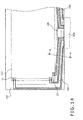
- FIG. 19 is a sectional view taken along line A-A of FIG. 14 , in the case where the ground layer is formed between the metallic wiring conductors 19A corresponding to the transmitting conductors 11 and the metallic wiring conductors 19B corresponding to the receiving conductors 13. That is, FIG. 19 corresponds to case (4) described above.
- the metallic wiring conductors 19A and the metallic wiring conductors 19B are both formed on the first glass substrate 15, and a ground layer 124 is disposed between the metallic wiring conductors 19A and the metallic wiring conductors 19B, with a predetermined gap between the metallic wiring conductors 19A and the ground layer 124 and a predetermined gap between the metallic wiring conductors 19B and the ground layer 124.
- the ground layer 124 has a longitudinal shape so as to separate the transmitting conductors 11 and the receiving conductors 13 from each other in parallel with the extending direction of the transmitting conductors 11 and the receiving conductors 13.
- the ground layer 124 is grounded similarly to the ground layer 120, described above. Because the ground layer 124 is disposed between the metallic wiring conductors 19A and 19B, interference of signals between the metallic wiring conductors 19A and 19B can be reduced.
- FIG. 20 is a diagram showing a sample modification to the construction shown in FIG. 19 . While one ground layer 124 is formed between the metallic wiring conductors 19A and 19B in the construction of FIG. 19 , the ground layer 124 may be divided into two parts, that is, separated into a ground layer 124A adjacent to the metallic wiring conductors 19A and a ground layer 124B adjacent to the metallic wiring conductors 19B. This allows for further preventing variations in potential of the metallic wiring conductors 19A corresponding to the transmitting conductors 11 from propagating toward the side of the receiving conductors 13 via the ground layer 124A.
- the detecting sensor 100 even in the case where the metallic wiring conductors 19A and the metallic wiring conductors 19B are arranged adjacent to each other in the wiring region on the first glass substrate 15, because the ground layer 120 set to a predetermined potential is formed to overlap the metallic wiring conductors 19A, even when an indicator approaches the region where the metallic wiring conductors 19A and the metallic wiring conductors 19B are adjacent to each other, interference of signals between the metallic wiring conductors 19A and the metallic wiring conductors 19B can be reduced, and erroneous detection of the indicator can be prevented.
- terminal electrode 130 and the ground layer 121 which are set to a predetermined potential, are disposed between the metallic wiring conductors 19A and the metallic wiring conductors 19B, interference of signals in the region where the metallic wiring conductors 19A adjoin the metallic wiring conductors 19B can be reduced, and erroneous detection of an indicator can be prevented.
Landscapes
- Engineering & Computer Science (AREA)
- General Engineering & Computer Science (AREA)
- Theoretical Computer Science (AREA)
- Human Computer Interaction (AREA)
- Physics & Mathematics (AREA)
- General Physics & Mathematics (AREA)
- Computer Networks & Wireless Communication (AREA)
- Position Input By Displaying (AREA)
- Measurement Of Length, Angles, Or The Like Using Electric Or Magnetic Means (AREA)
Abstract
Description
- The present invention relates to a detecting sensor mounted on a surface of a display screen and configured to detect the position of an indicator, a method for manufacturing the detecting sensor, and an indicator position detecting device incorporating the detecting sensor.
- A capacitance type input device has been known, which is disposed on the surface of a display screen of a liquid crystal display device to detect the touching position of a finger of a user or the like, and to input information corresponding to a displayed indicated image (see, for example, Japanese Patent Laid-Open No.
2009-259203 FIGS. 1 to 11 ), hereinafter referred to as Patent Document 1). In the capacitance type input device, light transmitting electrode patterns that intersect each other are formed on the surface of a light transmitting substrate, and the position of a finger of a user is detected based on a change in capacitance, which occurs when the finger touches the surface. - In the capacitance type input device disclosed in
Patent Document 1, metallic wiring pieces 9a respectively drawn out from a first light transmittingelectrode pattern 11 and a second light transmittingelectrode pattern 12, which intersect each other, are arranged adjacent to each other near an edge portion of alight transmitting substrate 15, and terminals 19a at end portions of the metallic wiring pieces 9a are connected to a flexible board 19. An area excluding the metallic wiring pieces 9a forms an input region 10a on thelight transmitting substrate 15. However, when a finger of a user or the like touches a wiring region including the metallic wiring pieces 9a of the two kinds of light transmittingelectrode patterns electrode patterns - In one aspect, the present invention is directed to providing a detecting sensor capable of preventing erroneous detection when an indicator, such as a finger, touches a wiring region that surrounds an input region. The present invention is further directed to providing an indicator position detecting device incorporating such a detecting sensor, and a method for manufacturing such a detecting sensor.
- According to an embodiment of the present invention, a detecting sensor is provided, which includes a plurality of first sensor conductors arranged in a first direction and a plurality of second sensor conductors arranged in a second direction, which intersects the first direction; on a base material. The detecting sensor further includes a plurality of first signal lines electrically connected to the first sensor conductors, a plurality of second signal lines electrically connected to the second sensor conductors, and a first conductive pattern disposed between the first signal lines and the base material. The first conductive pattern is electrically insulated from the first signal lines, and is set to a predetermined electric potential. The first conductive pattern may be made of the same material as the first sensor conductors or the second sensor conductors.
- Accordingly, even when the first signal lines and the second signal lines are arranged adjacent to each other in a wiring region on the base material, the first conductive pattern set to the predetermined potential is formed to overlap the first signal lines and, therefore, even when an indicator approaches the region in which the first signal lines and the second signal lines are arranged adjacent to each other, signal interference between the first signal lines and the second signal lines can be reduced, and erroneous detection of the indicator can be prevented.
- In one aspect, preferably, an insulating material is disposed between the first signal lines and the first conductive pattern to electrically insulate the first signal lines from the first conductive pattern. Further preferably, the plurality of first sensor conductors and the plurality of second sensor conductors are arranged on the same surface side of the base material, and the same insulating material as the insulating material disposed between the first signal lines and the first conductive pattern may be arranged in intersection regions between the first sensor conductors and the second sensor conductors. It then becomes possible to simultaneously form the insulating material for insulating the first sensor conductors from the second sensor conductors and the insulating material for insulating the first signal lines from the base material, to simplify the manufacturing process to thereby reduce manufacturing cost.
- In another aspect, preferably, each of the first sensor conductors includes a plurality of conductor pieces, which are arranged between the plurality of second sensor conductors. Each of the first sensor conductors further includes one or more conductive elements disposed to overlap the insulating material in the intersection regions between the first sensor conductors and the second sensor conductors, respectively, such that each of the conductive elements electrically connects adjacent two of the plurality of conductor pieces to each other. It then becomes possible to form the first sensor conductors and the second sensor conductors as a single layer, to ensure their stable characteristics and to further simplify the manufacturing process to thereby reduce manufacturing cost.
- In another aspect, preferably, the conductive elements described above may be formed of the same material as that used to form the first signal lines or the second signal lines. It then becomes possible to simultaneously form the conductive elements for electrically connecting the plurality of conductor pieces to each other and the first signal lines or the second signal lines, to still further simplify the manufacturing process to thereby reduce manufacturing cost.
- In another aspect, preferably, the first signal lines and the second signal lines have higher conductivity than the first sensor conductors and the second sensor conductors. This would improve signal transmission characteristics by lowering the overall resistance of the first sensor conductors and the first signal lines as well as the overall resistance of the second sensor conductors and the second signal lines.
- In another aspect, preferably, a second conductive pattern set to a predetermined potential is disposed between the first signal lines and the second signal lines, in a region where the second signal lines are arranged in the vicinity of the first signal lines. In addition, preferably, the second conductive pattern is disposed to overlap the first conductive pattern and is electrically connected to the first conductive pattern. The second conductive pattern disposed between the first signal lines and the second signal lines, which are adjacent to each other, can reduce signal interference in a region where the first signal lines adjoin the second signal lines, to thereby prevent erroneous detection of an indicator.
- In another aspect, preferably, the second conductive pattern includes a first linear conductor and a second linear conductor each connected to a predetermined potential. The first linear conductor may be disposed to overlap the first conductive pattern to be electrically connected to the first conductive pattern, to be thereby set to a predetermined potential. It then becomes possible to further reduce electric coupling between the first signal lines, which correspond to the first linear conductor and the first conductive pattern, and the second signal lines, which correspond to the second linear conductor, to further reduce erroneous detection.
- In another aspect, preferably, the first linear conductor of the second conductive pattern is formed to have a wider width than the second linear conductor. Accordingly, when the strength of signals input to and output from the first signal lines and the first sensor conductors is high for example, an electric field created by the first signal lines having the high signal strength can be effectively blocked (cut off) by the wide first linear conductor.
- In another aspect, preferably, the first sensor conductors and the second sensor conductors have transparency, and so does an area of the base material in which the first sensor conductors and the second sensor conductors are arranged. It then becomes possible to arrange the detecting sensor over a display screen, to thereby enable position detection on the display screen.
- According to a further embodiment of the present invention, an indicator position detecting device is provided, which includes a detecting sensor as described above for detecting a position indicated by an indicator; and an electric circuit configured to supply transmission signals to the detecting sensor and to detect a position indicated by the indicator based on received signals obtained from the detecting sensor.
- Even in the case where the first signal lines and the second signal lines are arranged adjacent to each other in a wiring region on the base material of the detecting sensor, the first conductive pattern set to the predetermined potential is formed to overlap the first signal lines and, therefore, even when an indicator approaches the region in which the first signal lines and the second signal lines are arranged adjacent to each other, signal interference between the first signal lines and the second signal lines can be reduced, and erroneous detection of the indicator can be prevented.
- According to a still further embodiment of the present invention, a method is provided for manufacturing a detecting sensor including a plurality of first sensor conductors arranged in a first direction and a plurality of second sensor conductors arranged in a second direction, which intersects the first direction, on one surface of a base material having transparency. The method includes generally six steps. First, a conductive film having transparency is formed on one surface of the base material using a metallic film forming process. Second, the plurality of second sensor conductors, a plurality of conductor pieces arranged between the plurality of second sensor conductors (to thereby form the plurality of first sensor conductors), and a first conductive pattern in a predetermined region are formed, by processing the conductive film. Third, an insulating material is disposed over the one surface of the base material. Fourth, the insulating material is left in each of regions between the conductor pieces, where the second sensor conductors are interposed between adjacent two of the conductor pieces, and also in a region of the first conductive pattern, by processing the insulating material. Fifth, a metallic film having higher conductivity than the conductive film is formed over the one surface of the base material, by a metallic film forming process. Sixth, the metallic film is processed such that the metallic film is left to overlap the insulating material, so as to electrically connect the plurality of conductor pieces to each other to form the first sensor conductors, to form first signal lines that are electrically connected to one ends of the first sensor conductors and that are disposed over the first conductive pattern with the insulating material interposed between the first signal lines and the first conductive pattern, and to form second signal lines that are electrically connected to one ends of the second sensor conductors.
- With the detecting sensor manufactured according to various embodiments of the present invention, even in the case where the first signal lines and the second signal lines are arranged adjacent to each other in a wiring region on the base material the first conductive pattern set to the predetermined potential is formed to overlap the first signal lines and, therefore, even when an indicator approaches the region in which the first signal lines and the second signal lines are arranged adjacent to each other, signal interference between the first signal lines and the second signal lines can be reduced, and erroneous detection of the indicator can be prevented.
-
-
FIG. 1 is a diagram schematically showing an external shape of an indicator position detecting device according to an embodiment; -
FIG. 2 is a diagram showing an overall configuration of the indicator position detecting device; -
FIG. 3 is a sectional view of a sensor section; -
FIG. 4 is a diagram showing a detailed configuration of a multi-frequency signal supplying circuit; -
FIG. 5 is a diagram showing a detailed configuration of a transmitting conductor selecting circuit; -
FIG. 6 is a diagram showing a detailed configuration of a receiving conductor selecting circuit and an amplifying circuit; -
FIGS. 7A and 7B are reference diagrams for illustrating signal levels detected by a signal detecting circuit; -
FIG. 8 is a plan view of the sensor section; -
FIG. 9 is a partial enlarged plan view of a detection region; -
FIG. 10 is a partial enlarged view showing details of one transmitting conductor positioned in a transmitting region and two receiving conductors intersecting the transmitting conductor; -
FIG. 11 is a sectional view along the longitudinal direction of the transmitting conductor ofFIG. 10 , which is positioned in the transmitting region; -
FIG. 12 is a partial enlarged view showing details of one transmitting conductor, which is partially positioned in a non-transmitting region, and two receiving conductors intersecting the transmitting conductor; -
FIG. 13 is a sectional view along the longitudinal direction of the transmitting conductor ofFIG. 12 , which is partially positioned in the non-transmitting region; -
FIG. 14 is a plan view partially detailing a wiring region shown inFIG. 8 ; -
FIG. 15 is a sectional view taken along line A-A ofFIG. 14 , in a case where a ground layer is formed between metallic wiring conductors corresponding to transmittingconductors 11 and a first glass substrate; -
FIG. 16 is a diagram showing sample modification to the construction ofFIG. 15 ; -
FIG. 17 is a sectional view taken along line A-A ofFIG. 14 , in a case where a ground layer is formed between metallic wiring conductors corresponding to receiving conductors and the first glass substrate; -
FIG. 18 is a sectional view taken along line A-A ofFIG. 14 , in a case where a ground layer is formed between both of the metallic wiring conductors corresponding to the transmitting conductors and the metallic wiring conductors corresponding to the receiving conductors and the first glass substrate; -
FIG. 19 is a sectional view taken along line A-A ofFIG. 14 , in a case where a ground layer is formed between the metallic wiring conductors corresponding to the transmitting conductors and the metallic wiring conductors corresponding to the receiving conductors; -
FIG. 20 is a diagram showing sample modification to the construction ofFIG. 19 ; -
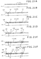
FIGS. 21A, 21B, 21C, 21D, 21E, and 21F are diagrams representing a process of manufacturing a detecting sensor having the construction shown inFIG. 15 ; and -
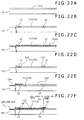
FIGS. 22A, 22B, 22C, 22D, 22E, and 22F are diagrams representing a process of manufacturing a detecting sensor having the construction shown inFIG. 19 . - An indicator position detecting device according to exemplary embodiments of the present invention will hereinafter be described with reference to the drawings.
- The use of ordinals such as first, second and third does not necessarily imply a ranked sense of order, but rather may only distinguish between multiple instances of a structure, act or value. For example, first and second groups may only distinguish between two groups, which may be interchangeable.
-
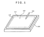
FIG. 1 is a diagram schematically showing an external shape of an indicator position detecting device according to an embodiment. The indicator position detecting device according to the present embodiment includes adisplay device 200, such as an LCD (Liquid Crystal Display) or the like, and a detectingsensor 100 for detecting a position indicated by anindicator 300 such as a finger of a user or the like. The detectingsensor 100 is disposed to overlap the display screen of thedisplay device 200. As used herein, the "indicator" includes a pen, which has a conductor in its tip section and which is detected by drawing up an electrostatic field through a path via a human body to ground based on the same principle as that of finger detection, and a pen configured to itself transmit a signal. - In
FIG 1 , the detectingsensor 100 has adetection region 112, though which the display screen of thedisplay device 200 that the detectingsensor 100 overlaps is visible and which defines an area for detecting a position of theindicator 300. As illustrated, awiring region 116 is set on the periphery of (i.e., to surround) thedetection region 112. -
FIG. 2 is a diagram showing an overall configuration of the indicator position detecting device. As shown inFIG. 2 , the indicator position detecting device includes the detectingsensor 100 and electric circuitry composed of a transmittingsection 20, a receivingsection 30, and acontrol circuit 40. The detectingsensor 100 has a conductor pattern formed of a transmittingconductor group 12 and a receivingconductor group 14. The transmittingconductor group 12 is formed of transmitting conductors 11 (i.e., first sensor conductors), which are a plurality of transparent conductors arranged at equal intervals in a predetermined direction (i.e., a first direction), and the receivingconductor group 14 is formed of receiving conductors 13 (i.e., second sensor conductors), which are a plurality of transparent conductors arranged at equal intervals in a direction (i.e., a second direction) orthogonal to the first direction in which the plurality of transmittingconductors 11 are arranged. -
FIG. 3 is a sectional view of the detectingsensor 100, and shows a partial cross section along one transmittingconductor 11. In the detectingsensor 100 of the illustrated embodiment, both of the transmittingconductors 11 and the receivingconductors 13 are formed on one surface of afirst glass substrate 15, which serves as a transparent base material in the illustrated embodiment. Asecond glass substrate 17, which is also a transparent substrate, is additionally disposed over the surfaces of both the transmittingconductors 11 and the receivingconductors 13, with aspacer 16 interposed therebetween. Further, as shown inFIG. 3 , the transmittingconductor 11 is divided into a plurality ofconductor pieces 11A in a longitudinal direction (i.e., in a direction in which the transmittingconductor 11 extends), which are separated by gaps formed at positions where the receivingconductors 13 are disposed. In addition, ametallic jumper wire 18, which serves as a conductive element, is formed so as to straddle each of the receivingconductors 13. Thus, twoconductor pieces 11A adjacent to each other are electrically connected to each other via themetallic jumper wire 18. - The transmitting
conductors 11 and the receivingconductors 13 have the shape of a flat plate, and are formed of a transparent electrode film made of an ITO (Indium Tin Oxide) film, for example. In the present embodiment, for example, 64 transmittingconductors 11 are arranged in a vertical direction (Y-direction) at predetermined intervals, and 128 receivingconductors 13 are arranged in a horizontal direction (X-direction) at predetermined intervals. InFIG. 2 , Y0 to Y63 respectively correspond to the 64 transmittingconductors 11, and X0 to X127 respectively correspond to the 128 respective receivingconductors 13. - The
spacer 16 is an insulator and is formed of, for example, PVB (PolyVinyl Butyral), EVA (Ethylene Vinyl Acetate), or a silicon rubber. The first andsecond glass substrates - The transmitting
section 20 shown inFIG. 2 includes aclock generating circuit 21, a multi-frequencysignal supplying circuit 22, and a transmittingconductor selecting circuit 23. Theclock generating circuit 21 generates a reference signal of a predetermined frequency. The multi-frequencysignal supplying circuit 22 generates, for example, 16 kinds of signals of frequencies f0, f1,..., and f15, respectively, using the reference signal output from theclock generating circuit 21, and outputs these signals in parallel with each other. InFIG. 2 , the transmittingconductor selecting circuit 23 is illustrated as being connected to the right end of each transmittingconductor 11. In an exemplary embodiment, however, the transmittingconductor selecting circuit 23 may be connected to both of the right end and the left end of each transmittingconductor 11, so that a signal is input from both ends of each transmittingconductor 11. -
FIG. 4 is a diagram showing a detailed configuration of the multi-frequencysignal supplying circuit 22. The multi-frequencysignal supplying circuit 22 includes 16 signal generating sections 22-0, 22-1, ..., and 22-15 for generating the 16 kinds of signals of frequencies f0, f1, ..., and f15, respectively. The signal generating sections 22-0 to 22-15 respectively generate the signals of frequencies f0 to f15 based on the reference signal output from theclock generating circuit 21. For example, the signal generating sections 22-0 to 22-15 generate the signals of the predetermined frequencies by frequency-dividing or multiplying the reference signal output from theclock generating circuit 21. Alternatively, the signal generating sections 22-0 to 22-15 may each have a waveform data ROM retaining waveform data of a sine wave, wherein periods of the sine waves retained in different waveform data ROMs are different from each other. The signal generating sections 22-0 to 22-15 may then generate sine wave signals of frequencies f0 to f15 by reading out the waveform data in synchronism with the reference signal output from theclock generating circuit 21. - The transmitting
conductor selecting circuit 23 selects transmittingconductors 11 as destinations, to which the 16 signals output in parallel with each other from the multi-frequencysignal supplying circuit 22 are to be supplied, and sequentially changes (switches) the transmittingconductors 11 as the selected destinations. -
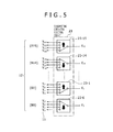
FIG. 5 is a diagram showing a detailed configuration of the transmittingconductor selecting circuit 23. The transmittingconductor selecting circuit 23 includes 16 selector switches 23-0, 23-1, ..., and 23-15, to which the 16 kinds of signals of frequencies f0, f1, ..., and f15 are input separately from each other. In the present embodiment, the 64 transmittingconductors 11 are divided and grouped (sectioned) into 16 blocks, B0 to B15. - Block B0 includes four transmitting
conductors 11 indicated by Y0 to Y3, which are arranged adjacent to each other. The selector switch 23-0 repeatedly changes thedestination transmitting conductor 11, to which the signal of frequency f0 output from the signal generating section 22-0 is supplied, in order of Y3, Y2, Y1, and Y0 at predetermined time intervals. InFIG. 5 , a direction in which the transmittingconductors 11 are changed is indicated by an arrow inside each of the selector switches 23-0 to 23-15. - Block B1 includes four transmitting
conductors 11 indicated by Y4 to Y7, which are arranged adjacent to each other. The selector switch 23-1 repeatedly changes thedestination transmitting conductor 11, to which the signal of frequency f1 output from the signal generating section 22-1 is supplied, in order of Y4, Y5, Y6, and Y7 at predetermined time intervals. - The same applies to the other blocks B2 to B15 and the other selector switches 23-2 to 23-15. The selector switches 23-2 to 23-15 each repeatedly changes the
destination transmitting conductor 11, to which the signal output from the corresponding signal generating section 22-2 to 22-15 is supplied, in predetermined order and at predetermined time internals. - The receiving
section 30 shown inFIG. 2 includes a receivingconductor selecting circuit 31, an amplifyingcircuit 32, an analog-to-digital converter circuit (A/D) 33, asignal detecting circuit 34, and aposition calculating circuit 35. -
FIG. 6 is a diagram showing a detailed configuration of the receivingconductor selecting circuit 31 and the amplifyingcircuit 32. The receivingconductor selecting circuit 31 includes 16 selector switches 31-0, 31-1, ..., and 31-15, each being configured to sequentially select corresponding eight receivingconductors 13. In the present embodiment, the 128 receivingconductors 13 are divided and grouped (sectioned) into 16 blocks, D0 to D15. - Block D0 includes eight receiving
conductors 13 indicated by X0 to X7, which are arranged adjacent to each other. The selector switch 31-0 selects one of the eight receivingconductors 13, and repeatedly changes the selection state in order of X0, X1, X2, X3, X4, X5, X6, and X7 at predetermined time intervals. InFIG. 6 , a direction in which the receivingconductors 13 are changed (switched) is indicated by an arrow inside each of the selector switches 31-0 to 31-15. - Block D1 includes eight receiving
conductors 13 indicated by X8 to X15, which are arranged adjacent to each other. The selector switch 31-1 selects one of the eight receivingconductors 13, and repeatedly changes the selection state in order of X15, X14, X13, X12, X11 X10, X9, and X8 at predetermined time intervals, - The same applies to the other blocks D2 to D15 and the other selector switches 31-2 to 31-15. The selector switches 31-2 to 31-15 each selects one of eight receiving
conductors 13, which are arranged adjacent to each other and are included in the corresponding block D2 to D15, and repeatedly changes the selection state in predetermined order and at predetermined time intervals. - The amplifying
circuit 32 includes 16 current-to-voltage converter circuits (I/V) 32-0, 32-1, ..., and 32-15 and aselector switch 32A. The current-to-voltage converter circuits 32-0 to 32-15 are each in one-to-one correspondence with the selector switches 31-0 to 31-15. Each of the current-to-voltage converter circuits 32-0 to 32-15 amplifies a current I output from a receivingconductor 13 selected by the corresponding selector switch 31-0 to 31-15, respectively, with a predetermined gain, and converts the current I into a voltage V. Theselector switch 32A sequentially selects signals (voltages) output from the 16 current-to-voltage converter circuits 32-0 to 32-15, and inputs the selected signals to the analog-to-digital converter circuit 33. - The analog-to-
digital converter circuit 33 converts the respective output voltages of the 16 current-to-voltage converter circuits 32-0 to 32-15, which are selected in order by theselector switch 32A, into data comprised of a predetermined number of bits. - The
signal detecting circuit 34 shown inFIG. 2 detects signal levels of 16 signal components corresponding to frequencies f0, f1, ..., and f15 output from the multi-frequencysignal supplying circuit 22 based on the data output from the analog-to-digital converter circuit 33. -
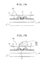
FIGS. 7A and 7B are reference diagrams for illustrating signal levels detected by thesignal detecting circuit 34.FIG. 7A shows a state in which a human finger as an indicator is not near a cross point of a transmittingconductor 11 and a receiving conductor 13 (i.e., a position where the transmittingconductor 11 and the receivingconductor 13 intersect each other).FIG. 7B shows a state in which a finger is near the cross point. As shown inFIG. 7A , when the finger is not near the cross point, the transmittingconductor 11 and the receivingconductor 13 are capacitively coupled to each other via thespacer 16 at the cross point, and an electric field emitted from the transmittingconductor 11 converges to the receivingconductor 13. Thus, when a signal of a predetermined frequency (one of frequencies f0 to f15) is supplied to the transmittingconductor 11, a current corresponding to the degree of the capacitive coupling can be extracted from the receivingconductor 13, which is capacitively coupled to the transmittingconductor 11. On the other hand, as shown inFIG. 7B , when the finger is near the cross point, while a current can be extracted from the receivingconductor 13 as in the case when the finger is not near the cross point, the degree of capacitive coupling between the transmittingconductor 11 and the receivingconductor 13 differs from that of the case when the finger is not near the cross point. That is, because a portion of an electric field emitted from the transmittingconductor 11 converges to the finger, the degree of capacitive coupling between the transmittingconductor 11 and the receivingconductor 13 is weakened, and the current extracted from the receivingconductor 13 is decreased. - In the present embodiment, 16 transmitting
conductors 11 that intersect one receivingconductor 13 are respectively supplied with 16 kinds of signals of frequencies f0, f1, ..., and f15 in parallel with each other. Thus, data corresponding to the receivingconductor 13 includes these 16 kinds of frequency components. Thesignal detecting circuit 34 extracts these 16 kinds of frequency components separately from each other (for example, it extracts the frequency components by performing synchronous detection), and detects a signal level corresponding to each of the frequency components. - The signal levels detected by the
signal detecting circuit 34 are stored, to be associated with the positions of the cross points. For example, combinations of Y0 to Y63 identifying the transmittingconductors 11 and X0 to X127 identifying the receivingconductors 13 are used as addresses to indicate the positions of cross points, and combinations of the addresses and the signal levels corresponding to the cross points are stored. When 16 kinds of frequency components included in a signal output from one receivingconductor 13 are known, because it is also known to which transmittingconductor 11 within each of the blocks B0 to B15 of the transmitting conductor group 12 a signal is supplied at any given point in time, aspecific transmitting conductor 11 can be identified as a destination to which the signal at each frequency is supplied. - When one cycle of the changing operations of the selector switches 23-0 to 23-15 within the transmitting
conductor selecting circuit 23 and the changing operations of the selector switches 31-0 to 31-15 within the receivingconductor selecting circuit 31 has been completed, that is, when the signal levels at all of the cross points are detected where the transmittingconductors 11 of the transmittingconductor group 12 and the receivingconductors 13 of the receivingconductor group 14 intersect each other in the detectingsensor 100, theposition calculating circuit 35 calculates a cross point, at which a signal level is lowered, as a position where a finger (indicator 300) is near. - Construction of the indicator position detecting device according to one embodiment has been described. Next, details of the detecting
sensor 100 will be described. -
FIG. 8 is a plan view of the detectingsensor 100. As shown inFIG. 8 , the detectingsensor 100 has adetection region 112, which occupies a large part in the center of the detectingsensor 100, and awiring region 116 disposed to surround the periphery of thedetection region 112. Thedetection region 112 includes a transmittingregion 110, through which the display screen of thedisplay device 200 that the detectingsensor 100 overlaps is visible. Thedetection region 112 also includes anon-transmitting region 114 having a predetermined width, which is provided on the periphery of the transmittingregion 110. -
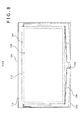
FIG. 9 is a partial enlarged plan view of thedetection region 112, and shows a construction as viewed from an opposite side from a surface to be touched by theindicator 300. As described above, thedetection region 112 is set, which is wider by a predetermined width than the transmittingregion 110 along its periphery. Thus, thedetection region 112 includes both the transmittingregion 110 and thenon-transmitting region 114, which has a predetermined width and which surrounds the periphery of the transmittingregion 110. If thedisplay device 200 has a horizontally long display screen and is disposed at an inclination nearly perpendicular to a ground surface, the plurality of transmittingconductors 11 arranged in parallel with each other extend such that their longitudinal direction is a horizontal direction, and the plurality of receivingconductors 13 arranged in parallel with each other extend such that their longitudinal direction is a vertical direction. Further, the transmitting and receivingconductors region 110 and thenon-transmitting region 114 of thedetection region 112. -
FIG. 10 is a partial enlarged view showing details of one transmittingconductor 11 positioned in the transmittingregion 110 and two receivingconductors 13 that intersect the transmittingconductor 11. As shown inFIG. 10 , the transmittingconductor 11 extending in the horizontal direction consists of a plurality ofconductor pieces 11A, which are separated by gaps formed at the positions where the transmitting conductor 11 I intersects the receivingconductors 13. Ametallic jumper wire 18 establishes an electrical connection between twoconductor pieces 11 A, which are adjacent to each other while sandwiching a gap therebetween. Each of the receivingconductors 13 extending in the vertical direction is formed as one continuous conductor, though a portion of the receivingconductor 13 that corresponds to the gap in the transmittingconductor 11 is made narrower than other portions of the receivingconductor 13. -
FIG. 11 is a sectional view along the longitudinal direction of the transmittingconductor 11, which is positioned in the transmittingregion 110, and shows themetallic jumper wire 18 and a structure around themetallic jumper wire 18. As shown inFIG. 11 , themetallic jumper wire 18 connects end parts of twoconductor pieces 11A that adjoin each other and that sandwich a gap therebetween. Themetallic jumper wire 18 is separated from a receivingconductor 13 disposed in the gap, to ensure electric insulation by interposing an insulating material between themetallic jumper wire 18 and the receivingconductor 13. -
FIG. 12 is a partial enlarged view showing details of one transmittingconductor 11, which is partially positioned in thenon-transmitting region 114, and two receivingconductors 13 which intersect the transmittingconductor 11. As shown inFIG. 12 , in thenon-transmitting region 114, the transmittingconductor 11 extending in the horizontal direction includes a plurality ofconductor pieces 11A separated by gaps formed at the positions where the transmittingconductor 11 intersects the receivingconductors 13. Ametallic jumper wire 18 establishes an electrical connection between twoconductor pieces 11A, which are adjacent to each other and which sandwich a gap therebetween. The transmittingconductor 11 positioned in thenon-transmitting region 114 further includes ametallic wiring pattern 11C formed integrally with themetallic jumper wire 18 along a longitudinal direction on the surface of each of theconductor pieces 11A. That is, as compared with the construction in the transmittingregion 110 shown inFIG. 10 , the construction in thenon-transmitting region 114 shown inFIG. 12 is different in that themetallic wiring pattern 11C is added, whereas the shape, arrangement and the like of the transmitting conductor 11 (consisting of theconductor pieces 11A) and the receivingconductor 13 themselves are the same. Thismetallic wiring pattern 11C is formed by directly extending themetallic jumper wire 18 formed at a boundary between thenon-transmitting region 114 and the transmittingregion 110 into thenon-transmitting region 114 along the transmittingconductor 11. -
FIG. 13 is a sectional view along the longitudinal direction of the transmittingconductor 11 ofFIG. 12 , which is partially positioned in thenon-transmitting region 114, and shows themetallic jumper wire 18 and themetallic wiring pattern 11C as well as a structure surrounding themetallic jumper wire 18 and themetallic wiring pattern 11C. As shown inFIG. 13 , themetallic jumper wire 18 connects end parts of twoconductor pieces 11A that adjoin each other and that sandwich a gap therebetween. Themetallic jumper wire 18 is separated from a receivingconductor 13 disposed in the gap. Themetallic wiring pattern 11C, whose end part is electrically connected to themetallic jumper wire 18, is formed on the surface of the transmittingconductor 11 included in thenon-transmitting region 114, without an insulating layer being interposed between themetallic wiring pattern 11C and the transmittingconductor 11. -
FIG. 14 is a plan view partially detailing thewiring region 116 shown inFIG. 8 . As shown inFIG. 14 ,metallic wiring conductors 19A (i.e., first signal lines) are connected to the left end parts of the transmittingconductors 11. The plurality ofmetallic wiring conductors 19A corresponding to the respective left end parts of the plurality of transmittingconductors 11 are drawn out to the left side of thedetection region 112, thereafter routed in a downward direction along the left side of thedetection region 112, and further routed along the lower side of thedetection region 112 to the vicinity of the central part of the lower side of thedetection region 112. Though not shown, themetallic wiring conductors 19A, which form a first wiring pattern, are also connected to the right end parts of the transmittingconductors 11, and are routed in a similar manner. Specifically, the plurality ofmetallic wiring conductors 19A corresponding to the respective right end parts of the plurality of transmittingconductors 11 are drawn out to the right side of thedetection region 112, thereafter routed in a downward direction along the right side of thedetection region 112, and further routed along the lower side of thedetection region 112 to the vicinity of the central part of the lower side of thedetection region 112. - In addition,
metallic wiring conductors 19B (i.e., second signal lines) are connected to the lower end parts of the receivingconductors 13. The plurality ofmetallic wiring conductors 19B corresponding to the respective lower end parts of the plurality of receivingconductors 13 are drawn out to the lower side of thedetection region 112, and thereafter routed along the lower side of thedetection region 112 to the central part of the lower side of thedetection region 112. The end parts of themetallic wiring conductors detection region 112 are connected to aflexible board 400, on which the transmittingsection 20, the receivingsection 30, thecontrol circuit 40 and the like, as shown inFIG. 2 , are mounted. This connection may be made with an anisotropic conductive film (ACF), for example. - In the present embodiment, a ground layer connected to a predetermined potential (for example, to ground) is formed in a region within the
wiring region 116 where themetallic wiring conductors 19A that form the first wiring pattern and themetallic wiring conductors 19B that form the second wiring pattern are adjacent and close to each other (i.e., along the lower side of thedetection region 112 in the illustrated embodiment). As the position where the ground layer may be formed, the following four cases (1) to (4) may be considered, for example. By the way, it should be noted that the predetermined potential may be a fixed potential other than a ground potential. - Case (1) The ground layer may be formed between the
metallic wiring conductors 19A corresponding to the transmittingconductors 11 and a position indicated by the indicator 300 (i.e., between themetallic wiring conductors 19A and thefirst glass substrate 15 when theindicator 300 is to indicate a position from the side of thefirst glass substrate 15, as shown inFIG. 3 ). - Case (2) The ground layer may be formed between the
metallic wiring conductors 19B corresponding to the receivingconductors 13 and a position indicated by theindicator 300. - Case (3) The ground layer may be formed between both of the
metallic wiring conductors 19A corresponding to the transmittingconductors 11 and themetallic wiring conductors 19B corresponding to the receivingconductors 13 and a position indicated by theindicator 300. - Case (4) The ground layer may be formed between the
metallic wiring conductors 19A corresponding to the transmittingconductors 11 and themetallic wiring conductors 19B corresponding to the receivingconductors 13. -
FIG. 15 is a sectional view taken along line A-A ofFIG. 14 , in the case where the ground layer is formed between themetallic wiring conductors 19A corresponding to the transmittingconductors 11 and thefirst glass substrate 15. That is,FIG. 15 corresponds to case (1) described above. As shown inFIG. 15 , a ground layer 120 (i.e., a first conductive pattern) and an insulating layer 140 (i.e., an insulating material) are formed between themetallic wiring conductors 19A and thefirst glass substrate 15. Themetallic wiring conductors 19A are arranged on theground layer 120, with the insulatinglayer 140 interposed between themetallic wiring conductors 19A and theground layer 120. - The
ground layer 120 may be formed of the same material as that of the transmittingconductors 11 and the receiving conductors 13 (for example, a transparent electrode film made of an ITO film). In a process of forming the transmittingconductors 11 and the receivingconductors 13, theground layer 120 may be formed at the same time. Aterminal electrode 130, which forms a longitudinal second conductive pattern in the illustrated embodiment, is arranged along the extending direction of both of the transmittingconductors 11 and the receivingconductors 13, in the vicinity of an edge part of theground layer 120 toward the side of the receivingconductors 13, as shown. Theground layer 120 is grounded via theterminal electrode 130. - As shown in
FIG. 15 , aground layer 121, which also forms a longitudinal second conductive pattern, is arranged in parallel with theground layer 120 between the transmittingconductors 11 and the receivingconductors 13. Theground layer 121 has a longitudinal shape along the extending direction of the receivingconductors 13, and is grounded similarly to theground layer 120. Because theground layer 120 corresponding to the transmittingconductors 11 is formed separately from theground layer 121, which is adjacent to the receivingconductors 13, variations in potential are prevented from propagating between the ground layers 120 and 121. Also, because theground layer 121 does not overlap themetallic wiring conductors 19A nor themetallic wiring conductors 19B, theground layer 121 can be formed at the same time when themetallic wiring conductors 19A and themetallic wiring conductors 19B are formed using the same metallic conductor material. In the illustrated embodiment, theterminal electrode 130 corresponds to a first linear conductor, and theground layer 121 corresponds to a second linear conductor, which together form the second conductor pattern. - As shown in
FIG. 15 , theterminal electrode 130 is set to have a width that is wider as compared to that of theground layer 121, both of which lie between the transmittingconductors 11 and the receivingconductors 13. A comparison between the strength of signals input to and output from the transmittingconductors 11 and the strength of signals input to and output from the receivingconductors 13 shows that the strength of the signals input to and output from the transmittingconductors 11 is higher. By making theterminal electrode 130 on the side of the transmittingconductors 11 wider, it becomes possible to effectively block an electric field created by the transmittingconductors 11, which have the high signal strength, with the wideterminal electrode 130. -
FIG. 16 is a diagram showing a sample modification made to the construction ofFIG. 15 . In the construction ofFIG. 15 , theground layer 120 disposed between the transmittingconductors 11 and thefirst glass substrate 15 extends (or is exposed) toward the side of the receivingconductors 13, and theterminal electrode 130 is disposed on the extended (exposed) part of theground layer 120. On the other hand, in the modified example ofFIG. 16 , theground layer 120 is extended (exposed) not only toward the side of the receivingconductors 13 but also toward an opposite side from the receivingconductors 13, and theterminal electrodes 130 are disposed on both of the extended (exposed) parts of theground layer 120, respectively. Thus, variations in potential of theground layer 120 as a whole can be further suppressed. -
FIG. 17 is a sectional view taken along line A-A ofFIG. 14 , in the case where the ground layer is formed between themetallic wiring conductors 19B corresponding to the receivingconductors 13 and thefirst glass substrate 15, That is,FIG. 17 corresponds to case (2) described above. As shown inFIG. 17 , aground layer 122 and an insulatinglayer 142 are formed between themetallic wiring conductors 19B and thefirst glass substrate 15. Themetallic wiring conductors 19B are arranged on theground layer 122, with the insulatinglayer 142 interposed between themetallic wiring conductors 19B and theground layer 122. - The
ground layer 122 may be formed of the same material as that of the transmittingconductors 11 and the receiving conductors 13 (for example, a transparent electrode film made of an ITO film). Thus, in a process of forming the transmittingconductors 11 and the receivingconductors 13, theground layer 122 may be formed at the same time. A longitudinalterminal electrode 132 is formed along the extending direction of both of the transmittingconductors 11 and the receivingconductors 13, in the vicinity of an edge part of theground layer 122 toward the side of the transmittingconductors 11. Theground layer 122 is grounded via theterminal electrode 132. - As shown in
FIG. 17 , aground layer 123 is formed in parallel with theground layer 122 between the transmittingconductors 11 and the receivingconductors 13. Theground layer 123 has a longitudinal shape along the extending direction of the transmittingconductors 11, and is grounded similarly to theground layer 122. Because theground layer 122 corresponding to the receivingconductors 13 is formed separately from theground layer 123 adjacent to the transmittingconductors 11, variations in potential are prevented from propagating between the ground layers 122 and 123. Also, because theground layer 123 does not overlap themetallic wiring conductors 19A nor themetallic wiring conductors 19B, theground layer 123 can be formed by using the same metallic conductor material and at the same time when themetallic wiring conductors 19A and themetallic wiring conductors 19B are formed. - In the construction shown in
FIG. 17 , theground layer 122 disposed between the receivingconductors 13 and thefirst glass substrate 15 is extended (exposed) toward the side of the transmittingconductors 11, and theterminal electrode 132 is disposed on the exposed part of theground layer 122. However, theground layer 122 may be extended (exposed) not only toward the side of the transmittingconductors 11 but also toward an opposite side from the transmittingconductors 11, and theterminal electrodes 132 may be disposed on both of the exposed parts of theground layer 122. Then, variations in potential of theground layer 122 as a whole can be further suppressed. -
FIG. 18 is a sectional view taken along line A-A ofFIG. 14 , in the case where the ground layer is formed between both of themetallic wiring conductors 19A corresponding to the transmittingconductors 11 and themetallic wiring conductors 19B corresponding to the receivingconductors 13 and thefirst glass substrate 15. That is,FIG. 18 corresponds to case (3) described above. As shown inFIG. 18 , aground layer 120 and an insulatinglayer 140 are formed between themetallic wiring conductors 19A and thefirst glass substrate 15, and aground layer 122 and an insulatinglayer 142 are formed between themetallic wiring conductors 19B and thefirst glass substrate 15. Themetallic wiring conductors 19A are arranged on theground layer 120, with the insulatinglayer 140 interposed between themetallic wiring conductors 19A and theground layer 120. Similarly, themetallic wiring conductors 19B are arranged on theground layer 122, with the insulatinglayer 142 interposed between themetallic wiring conductors 19B and theground layer 122. - The ground layers 120 and 122 may be formed of the same material as that of the transmitting
conductors 11 and the receiving conductors 13 (for example, a transparent electrode film made of an ITO film). Thus, in a process of forming the transmittingconductors 11 and the receivingconductors 13, the ground layers 120 and 122 may be also formed at the same time. A longitudinalterminal electrode 130 may be formed along the extending direction of the transmittingconductors 11 and the receivingconductors 13 in the vicinity of an edge part of theground layer 120 toward the side of the receivingconductors 13. Theground layer 120 is grounded via theterminal electrode 130. Another longitudinalterminal electrode 132 may be formed along the extending direction of the transmittingconductors 11 and the receivingconductors 13 in the vicinity of an edge part of theground layer 122 toward the side of the transmittingconductors 11. Theground layer 122 is grounded via theterminal electrode 132. Separating theground layer 120 from theground layer 122 in this manner prevents propagation of variations in potential between the ground layers 120 and 122. - A comparison between the
terminal electrode 130 and theterminal electrode 132 formed between the transmittingconductors 11 and the receivingconductors 13, in the example shown inFIG. 18 , shows that theterminal electrode 130 is set wider. A comparison between the strength of signals input to and output from the transmittingconductors 11 and the strength of signals input to and output from the receivingconductors 13 shows that the strength of the signals input to and output from the transmittingconductors 11 is higher. Setting theterminal electrode 130 on the side of the transmittingconductors 11 wider permits effectively blocking an electric field created by the transmittingconductors 11, which have the high signal strength, with the wideterminal electrode 130. -
FIG. 19 is a sectional view taken along line A-A ofFIG. 14 , in the case where the ground layer is formed between themetallic wiring conductors 19A corresponding to the transmittingconductors 11 and themetallic wiring conductors 19B corresponding to the receivingconductors 13. That is,FIG. 19 corresponds to case (4) described above. As shown inFIG. 19 , themetallic wiring conductors 19A and themetallic wiring conductors 19B are both formed on thefirst glass substrate 15, and aground layer 124 is disposed between themetallic wiring conductors 19A and themetallic wiring conductors 19B, with a predetermined gap between themetallic wiring conductors 19A and theground layer 124 and a predetermined gap between themetallic wiring conductors 19B and theground layer 124. Theground layer 124 has a longitudinal shape so as to separate the transmittingconductors 11 and the receivingconductors 13 from each other in parallel with the extending direction of the transmittingconductors 11 and the receivingconductors 13. Theground layer 124 is grounded similarly to theground layer 120, described above. Because theground layer 124 is disposed between themetallic wiring conductors metallic wiring conductors -
FIG. 20 is a diagram showing a sample modification to the construction shown inFIG. 19 . While oneground layer 124 is formed between themetallic wiring conductors FIG. 19 , theground layer 124 may be divided into two parts, that is, separated into aground layer 124A adjacent to themetallic wiring conductors 19A and aground layer 124B adjacent to themetallic wiring conductors 19B. This allows for further preventing variations in potential of themetallic wiring conductors 19A corresponding to the transmittingconductors 11 from propagating toward the side of the receivingconductors 13 via theground layer 124A. - Thus, in the detecting
sensor 100 according to various exemplary embodiments, even in the case where themetallic wiring conductors 19A and themetallic wiring conductors 19B are arranged adjacent to each other in the wiring region on thefirst glass substrate 15, because theground layer 120 set to a predetermined potential is formed to overlap themetallic wiring conductors 19A, even when an indicator approaches the region where themetallic wiring conductors 19A and themetallic wiring conductors 19B are adjacent to each other, interference of signals between themetallic wiring conductors 19A and themetallic wiring conductors 19B can be reduced, and erroneous detection of the indicator can be prevented. - In addition, the insulating
layer 140 for electrically insulating themetallic wiring conductors 19A from theground layer 120 may be disposed between themetallic wiring conductors 19A and theground layer 120, and the insulatinglayer 140 may be formed of the same insulating material used to provide electric insulation between theconductor pieces 11A of the transmittingconductors 11 and the receivingconductors 13. Thus, these insulating layer and materials can be formed simultaneously, to simplify the manufacturing process to thereby reduce manufacturing cost. In addition, forming the transmittingconductors 11 and the receivingconductors 13 as a single layer ensures their stable characteristics, while further simplifying the manufacturing process to thereby reduce manufacturing cost. - In addition, when the same material is used to form the
metallic jumper wires 18 that connect theconductor pieces 11A of the transmittingconductors 11 to each other, themetallic wiring conductors 19A, and themetallic wiring conductors 19B (or either of themetallic wiring conductors 19A or themetallic wiring conductors 19B), themetallic jumper wires 18 and themetallic wiring conductors - In addition, the
metallic wiring conductors 19A and themetallic wiring conductors 19B may have higher conductivity than the transmittingconductors 11 and the receivingconductors 13, to therefore improve signal transmission characteristics by lowering the overall resistance of the transmittingconductors 11 and themetallic wiring conductors 19A and the overall resistance of the receivingconductors 13 and themetallic wiring conductors 19B. - In addition, when the
terminal electrode 130 and theground layer 121, which are set to a predetermined potential, are disposed between themetallic wiring conductors 19A and themetallic wiring conductors 19B, interference of signals in the region where themetallic wiring conductors 19A adjoin themetallic wiring conductors 19B can be reduced, and erroneous detection of an indicator can be prevented. - Next, a concrete example of a process of manufacturing the detecting
sensor 100 is described.FIGS. 21A to 21F are diagrams representing a process of manufacturing the detectingsensor 100 shown inFIG. 15 . - (1) An
ITO film 211 as a conductive film having transparency is formed on one surface of afirst glass substrate 15, which is a transparent substrate that overlaps a display screen (first step,FIG. 21A ). - (2) The
ITO film 211 is processed (for example, by photolithography and etching), to thereby form receivingconductors 13,conductor pieces 11A, and aground layer 120 as a conductive pattern, out of theITO film 211 on one surface of the first glass substrate 15 (second step,FIG. 21B ). At this time, the receivingconductors 13 are formed in the shape of continuous lines, while theconductor pieces 11A are formed in the shape of dotted lines, which are broken at positions that intersect the receivingconductors 13. - (3) An insulating
layer 211 D (i.e., an insulating material) is formed on one surface of thefirst glass substrate 15, on which theconductor pieces 11A, the receivingconductors 13, and theground layer 120 have been formed, using a coater (third step,FIG. 21C ). - (4) The insulating
layer 211D is processed (for example, by photolithography and etching) to remove unnecessary portions of the insulatinglayer 211D, to thereby leave the insulatinglayer 211D in regions where theconductor pieces 11A intersect the receiving conductors 13 (i.e., regions between theconductor pieces 11 A where the receivingconductors 13 are disposed) and in an area for the ground layer 120 (fourth step,FIG. 21D ). Thus, an insulatinglayer 11D is formed in the regions where theconductor pieces 11A intersect the receivingconductors 13, and an insulatinglayer 140 is formed over theground layer 120. - (5) A
metallic layer 218, formed of a metallic film having higher conductivity than theconductor pieces 11A, the receivingconductors 13, and theground layer 120, is formed by applying a metallic film forming process (for example, by sputtering a metal) over one surface of thefirst glass substrate 15, on which theconductor pieces 11A, the receivingconductors 13, and theground layer 120 have been formed (fifth step,FIG. 21E ). - (6) The
metallic layer 218 is processed (for example, by photolithography and etching) to simultaneously formmetallic jumper wires 18, which respectively establish electric connections between twoadjacent conductor pieces 11A along the longitudinal direction of theconductor pieces 11A,metallic wiring conductors 19A over the insulatinglayer 140, a terminal electrode 130 (not shown inFIGS. 21A to 21F ) on theground layer 120, andmetallic wiring conductors 19B (not shown inFIGS. 21A to 21F ) over the first glass substrate 15 (sixth step,FIG. 21F ). Thereafter, an overcoat material is applied, to thereby complete the detectingsensor 100. - In the detecting
sensor 100 manufactured in this manner, even if the two kinds ofmetallic wiring conductors wiring region 116, theground layer 120 or the like is formed to overlap themetallic wiring conductors indicator 300 approaches thewiring region 116, interference of signals between themetallic wiring conductors 19A and themetallic wiring conductors 19B can be reduced, and erroneous detection of the indicator can be prevented. In addition, the transmittingconductors 11, the receivingconductors 13, and theground layer 120 or the like can all be formed of a transparent conductor material as a single layer. Thus, it is possible to achieve stable characteristics of the two kinds of conductors (the transmittingconductors 11 and the receiving conductors 13), and it becomes unnecessary to perform extra processing to add theground layer 120 or the like. Thus, high performance is achieved while at the same time manufacturing cost is suppressed. While the manufacturing process represented inFIGS. 21A to 21F corresponds to the construction shown inFIG. 15 , the process similarly applies to the construction shown inFIG. 16, FIG. 17 , andFIG. 18 . -
FIGS. 22A to 22F are diagrams representing a process of manufacturing the detectingsensor 100 shown inFIG. 19 . - (1) An
ITO film 211 as a conductive film having transparency is formed on one surface of afirst glass substrate 15, which is a transparent substrate that overlaps a display screen (first step,FIG. 22A ). - (2) The
ITO film 211 is processed (for example, by photolithography and etching), to thereby form receivingconductors 13 andconductor pieces 11 A out of theITO film 211 on one surface of the first glass substrate 15 (second step,FIG. 22B ). At this time, the receivingconductors 13 are formed in the shape of continuous lines, while theconductor pieces 11A are formed in the shape of dotted lines, which are broken at positions that intersect the receivingconductors 13. - (3) An insulating
layer 211D (i.e., an insulating material) is formed on one surface of thefirst glass substrate 15, on which theconductor pieces 11 A and the receivingconductors 13 have been formed, using a coater (third step,FIG. 22C ). - (4) The insulating
layer 211D is processed (for example, by photolithography and etching) to remove unnecessary portions of the insulatinglayer 211D, to thereby leave the insulatinglayer 211D in regions where theconductor pieces 11A intersect the receiving conductors 13 (i.e., regions between theconductor pieces 11A where the receivingconductors 13 are disposed) (fourth step,FIG. 22D ). Thus, an insulatinglayer 11D is formed in the regions where theconductor pieces 11A intersect the receivingconductors 13. - (5) A
metallic layer 218, formed of a metallic film having higher conductivity than theconductor pieces 11A and the receivingconductors 13, is formed by applying a metallic film forming process (for example, by sputtering a metal) over one surface of thefirst glass substrate 15, on which theconductor pieces 11A and the receivingconductors 13 have been formed (fifth step,FIG. 22E ). - (6) The
metallic layer 218 is processed (for example, by photolithography and etching) to simultaneously formmetallic jumper wires 18, which respectively establish electric connections between twoadjacent conductor pieces 11A along the longitudinal direction of theconductor pieces 11A, andmetallic wiring conductors ground layer 124 over the first glass substrate 15 (sixth step,FIG. 22F ). Thereafter, an overcoat material is applied, to thereby complete the detectingsensor 100. - In the detecting
sensor 100 manufactured in this manner, even if the two kinds ofmetallic wiring conductors wiring region 116, theground layer 124 is formed between themetallic wiring conductors indicator 300 approaches thewiring region 116, interference of signals between themetallic wiring conductors 19A and themetallic wiring conductors 19B can be reduced, and erroneous detection of the indicator can be prevented. While the manufacturing process represented inFIGS. 22A to 22F corresponds to the construction shown inFIG. 19 , the process similarly applies to the construction shown inFIG. 20 . - Those skilled in the art should appreciate that the present invention is not limited to the embodiments described above, and various modifications are possible and are within the scope of the present invention. For example, while the transmitting
conductors 11 are illustrated to be orthogonal to the receivingconductors 13 in each of the foregoing embodiments, the present invention is also applicable in cases where the transmittingconductors 11 intersect the receivingconductors 13 at an angle other than 90 degrees. - In addition, while each of the transmitting
conductor group 12 and the receivingconductor group 14 is segmented (grouped) into 15 blocks in each of the foregoing embodiments, the number of blocks may vary, and also the number of blocks of the transmittingconductor group 12 may be different from the number of blocks of the receivingconductor group 14. Also, circuitry may be provided to detect a current in each of the receivingconductors 13 included in the receivingconductor group 14, to thereby omit having to perform the changing (switching) operation over the receivingconductors 13. - In each of the above-described embodiments, multi-frequency signals are assumed as signals to be supplied to the transmitting
conductors 11. However, the signals to be supplied may be signals other than multi-frequency signals. For example, similar effects can be obtained in an indicator position detecting device, in which a plurality of spread code signals, or spread spectrum codes, are supplied to the transmittingconductors 11, which are divided into each block. Furthermore, similar effects can be also obtained in an indicator position detecting device, in which a specific spread code is used and shifted in phase, such that a plurality of phase-shifted codes (based on the same spread code) are supplied to the transmittingconductors 11, which are divided into each block. - In each of the above-described embodiments, the present invention is applied in a detecting
sensor 100 of the capacitance type, and in an indicator position detecting device, which supplies signals to the transmittingconductors 11 and which detects current output from the receivingconductors 13. However, the present invention is also applicable in an indicator position detecting device of the capacitance type, which detects respective capacitance values of two kinds of conductors (electrodes) intersecting each other to thereby detect the position of an indicator, as disclosed in Japanese Patent Laid-Open No.2009-162538 - In the foregoing embodiments, the transmitting conductors, the receiving conductors, the ground layer, and the like, are formed by using an ITO film as a conductive film having transparency. However, a conductive film having transparency other than an ITO film may be used. Also, when a focus is to reduce signal interference when an indicator approaches a region in which two kinds of signal lines (metallic wiring conductors) are arranged adjacent to each other, the transmitting conductors, the receiving conductors, the ground layer, and the like may be formed of a nontransparent material.
- According to the present invention, even in the case where the
metallic wiring conductors 19A (i.e., first signal lines) and themetallic wiring conductors 19B (i.e., second signal lines) are arranged adjacent to each other in the wiring region on thefirst glass substrate 15, theground layer 120 set to a predetermined potential is formed to overlap themetallic wiring conductors 19A and, therefore, even when an indicator approaches the region in which themetallic wiring conductors 19A and themetallic wiring conductors 19B are arranged adjacent to each other, interference of signals between themetallic wiring conductors 19A and themetallic wiring conductors 19B can be reduced, and erroneous detection of the indicator can be prevented. - It should be understood by those skilled in the art that various modifications, combinations, sub-combinations and alterations are possible depending on design requirements and other factors, and that they are within the scope of the appended claims or the equivalents thereof.
Claims (14)
- A detecting sensor for detecting a position indicated by an indicator, the detecting sensor comprising:a base material;a plurality of first sensor conductors arranged in a first direction;a plurality of first signal lines electrically connected to said first sensor conductors, respectively;a plurality of second sensor conductors arranged in a second direction intersecting said first direction;a plurality of second signal lines electrically connected to said second sensor conductors, respectively; anda first conductive pattern disposed between said first signal lines and said base material, the first conductive pattern being electrically insulated from said first signal lines, the first conductive pattern being set to a predetermined potential, and the first conductive pattern being made of a same material as that used to form either one of said first sensor conductors and said second sensor conductors.
- The detecting sensor according to claim 1, wherein
an insulating material for electrically insulating said first signal lines from said first conductive pattern is disposed between said first signal lines and said first conductive pattern, and
said plurality of first sensor conductors and said plurality of second sensor conductors are arranged on a same surface side of said base material, and a same insulating material as that used to form said insulating material disposed between said first signal lines and said first conductive pattern is arranged in intersection regions between said first sensor conductors and said second sensor conductors to thereby insulate said first sensor conductors from said second sensor conductors. - The detecting sensor according to claim 1 or 2, wherein said first sensor conductors include:a plurality of conductor pieces arranged between said plurality of second sensor conductors; andone or more conductive elements disposed to overlap said insulating material in the intersection regions between said first sensor conductors and said second sensor conductors,wherein said plurality of conductor pieces are electrically connected to each other by said one or more conductive elements.
- The detecting sensor according to claim 3, wherein
said one or more conductive elements are formed of a same material as that used to form at least one of said first signal lines and said second signal lines. - The detecting sensor according to one of the preceding claims, wherein
a second conductive pattern set to the predetermined potential is disposed between said first signal lines and said second signal lines in a region in which said plurality of second signal lines adjoins said plurality of first signal lines. - The detecting sensor according to claim 5, wherein
said second conductive pattern is disposed on said first conductive pattern, and is electrically connected to said first conductive pattern. - The detecting sensor according to claim 5 or 6, wherein
said second conductive pattern includes a first linear conductor and a second linear conductor both connected to said predetermined potential, and said first linear conductor is disposed on said first conductive pattern and is electrically connected to said first conductive pattern. - The detecting sensor according to claim 7, wherein
said plurality of second signal lines are arranged to receive signals from the plurality of second sensor conductors, respectively, and said first linear conductor of said second conductive pattern disposed on said first conductive pattern is formed to have a width greater than a width of said second linear conductor, wherein signals provided to said plurality of first signal lines have a greater signal strength than those signals received by the second signal lines from the second sensor conductors. - The detecting sensor according to one of the preceding claims, wherein
said first signal lines and said second signal lines have higher conductivity than said first sensor conductors and said second sensor conductors. - The detecting sensor according to one of the preceding claims, wherein
said first sensor conductors, said second sensor conductors, and a region of said base material in which said first sensor conductors and said second sensor conductors are arranged have transparency. - The detecting sensor according to one of the preceding claims , wherein
the first conductive pattern is additionally disposed between said second signal lines and said base material, the first conductive pattern being electrically insulated from said second signal lines. - The detecting sensor according to claim 11, wherein
the first conductive pattern includes a first layer, which is disposed between said first signal lines and said base material and is electrically insulated from said first signal lines, and a second layer, which is disposed between said second signal lines and said base material and is electrically insulated from said second signal lines. - An indicator position detecting device comprising:a detecting sensor according to one of the preceding claims configured to detect a position indicated by an indicator; andan electric circuit configured to supply a transmission signal to said detecting sensor and to detect the position indicated by said indicator based on a received signal obtained from said detecting sensor.
- A method for manufacturing a detecting sensor for detecting a position indicated by an indicator, the detecting sensor including a plurality of first sensor conductors arranged in a first direction and a plurality of second sensor conductors arranged in a second direction intersecting said first direction on one surface of a base material having transparency, the method comprising:forming, on the one surface of said base material by a metallic film forming process, said plurality of second sensor conductors having transparency, a plurality of conductor pieces having transparency for forming said plurality of first sensor conductors, the plurality of conductor pieces being arranged between said plurality of second sensor conductors, and a first conductive pattern in a predetermined region;disposing an insulating material in each of regions between said conductor pieces, said second sensor conductors being arranged in said regions, and in a region corresponding to said first conductive pattern on said one surface of said base material; andby a metallic film forming process, disposing a metallic film, which has higher conductivity than the plurality of said first sensor conductors, said second sensor conductors, and said first conductive pattern, over said insulating material, to thereby electrically connect said plurality of conductor pieces to form said first sensor conductors, to form first signal lines that are electrically connected to one ends of said first sensor conductors and that are disposed over said first conductive pattern, with said insulating material interposed between the first signal lines and said first conductive pattern, and to form second signal lines that are electrically connected to one ends of said second sensor conductors.
Applications Claiming Priority (1)
| Application Number | Priority Date | Filing Date | Title |
|---|---|---|---|
| JP2010268062A JP5730551B2 (en) | 2010-12-01 | 2010-12-01 | Detection sensor for detecting an indication position by an indicator, an indicator position detection device, and a method for manufacturing the detection sensor |
Publications (3)
| Publication Number | Publication Date |
|---|---|
| EP2461240A2 true EP2461240A2 (en) | 2012-06-06 |
| EP2461240A3 EP2461240A3 (en) | 2014-12-03 |
| EP2461240B1 EP2461240B1 (en) | 2020-10-21 |
Family
ID=45318850
Family Applications (1)
| Application Number | Title | Priority Date | Filing Date |
|---|---|---|---|
| EP11191152.5A Active EP2461240B1 (en) | 2010-12-01 | 2011-11-29 | Detecting sensor, indicator position detecting device, and method for manufacturing detecting sensor |
Country Status (6)
| Country | Link |
|---|---|
| US (1) | US9052784B2 (en) |
| EP (1) | EP2461240B1 (en) |
| JP (1) | JP5730551B2 (en) |
| KR (1) | KR101943649B1 (en) |
| CN (2) | CN102591539B (en) |
| TW (1) | TWI545467B (en) |
Families Citing this family (7)
| Publication number | Priority date | Publication date | Assignee | Title |
|---|---|---|---|---|
| JP5730551B2 (en) * | 2010-12-01 | 2015-06-10 | 株式会社ワコム | Detection sensor for detecting an indication position by an indicator, an indicator position detection device, and a method for manufacturing the detection sensor |
| US9791487B2 (en) * | 2012-03-29 | 2017-10-17 | Egalax_Empia Technology Inc. | Method and device for measuring signals |
| CN102724811B (en) * | 2012-06-13 | 2015-05-06 | 深圳市华星光电技术有限公司 | Liquid crystal display device and PCB (printed circuit board) for same |
| US9107328B2 (en) | 2012-06-13 | 2015-08-11 | Shenzhen China Star Optoelectronics Technology Co., Ltd. | PCB for LCD device and LCD device |
| US9547400B2 (en) * | 2014-04-25 | 2017-01-17 | Synaptics Incorporated | Interference detection using frequency modulation |
| USD834647S1 (en) * | 2017-11-02 | 2018-11-27 | Art Design Works LLC | Pencil holder |
| KR102779222B1 (en) | 2020-05-12 | 2025-03-11 | 삼성전자주식회사 | Fingerprint Sensor and Electronic device comprising Fingerprint Sensor |
Citations (2)
| Publication number | Priority date | Publication date | Assignee | Title |
|---|---|---|---|---|
| JP2009162538A (en) | 2007-12-28 | 2009-07-23 | Wacom Co Ltd | Position detection device |
| JP2009259203A (en) | 2008-03-25 | 2009-11-05 | Epson Imaging Devices Corp | Capacitive input device, display device with input function, and electronic apparatus |
Family Cites Families (17)
| Publication number | Priority date | Publication date | Assignee | Title |
|---|---|---|---|---|
| JPH09146682A (en) * | 1995-11-29 | 1997-06-06 | Fujitsu Takamizawa Component Kk | Coordinate input device |
| WO2004112448A2 (en) * | 2003-06-13 | 2004-12-23 | Semtech Corporation | Sensor for capacitive touch pad pointing device |
| JP2006029987A (en) * | 2004-07-16 | 2006-02-02 | Alps Electric Co Ltd | Capacitance type detection device and method, and coordinate detecting program |
| US7358741B2 (en) | 2004-05-25 | 2008-04-15 | Alps Electric Co., Ltd | Electrostatic detection apparatus and method, and coordinate detection program |
| JP4435622B2 (en) | 2004-05-25 | 2010-03-24 | アルプス電気株式会社 | Capacitance type detection device |
| US7932898B2 (en) * | 2005-09-20 | 2011-04-26 | Atmel Corporation | Touch sensitive screen |
| JP2009169720A (en) * | 2008-01-17 | 2009-07-30 | Smk Corp | Touch sensor |
| JP4582169B2 (en) * | 2008-03-26 | 2010-11-17 | ソニー株式会社 | Capacitance type input device, display device with input function, and electronic device |
| JP5113773B2 (en) | 2009-01-20 | 2013-01-09 | 株式会社ジャパンディスプレイイースト | Display device |
| KR101304787B1 (en) * | 2009-03-20 | 2013-09-05 | 티피케이 터치 솔루션즈 (씨아먼) 인코포레이티드 | Capacitive touch circuit pattern and manufacturing method thereof |
| JP5106471B2 (en) * | 2009-04-24 | 2012-12-26 | 三菱電機株式会社 | Touch panel and display device including the same |
| JP5316216B2 (en) * | 2009-05-18 | 2013-10-16 | 富士通株式会社 | Association processing method and flow comparison processing apparatus |
| JP2010267223A (en) * | 2009-05-18 | 2010-11-25 | Seiko Epson Corp | Touch panel manufacturing method, display device manufacturing method, and electronic device manufacturing method |
| JP2010271796A (en) * | 2009-05-19 | 2010-12-02 | Optrex Corp | Connection structure between electrodes and touch panel |
| CN201465085U (en) | 2009-06-05 | 2010-05-12 | 深圳莱宝高科技股份有限公司 | Capacitance touch screen wiring |
| TWI380209B (en) * | 2009-06-18 | 2012-12-21 | Au Optronics Corp | Touch panel |
| JP5730551B2 (en) * | 2010-12-01 | 2015-06-10 | 株式会社ワコム | Detection sensor for detecting an indication position by an indicator, an indicator position detection device, and a method for manufacturing the detection sensor |
-
2010
- 2010-12-01 JP JP2010268062A patent/JP5730551B2/en not_active Expired - Fee Related
-
2011
- 2011-11-15 US US13/296,662 patent/US9052784B2/en active Active
- 2011-11-25 KR KR1020110124279A patent/KR101943649B1/en not_active Expired - Fee Related
- 2011-11-25 TW TW100143339A patent/TWI545467B/en not_active IP Right Cessation
- 2011-11-29 EP EP11191152.5A patent/EP2461240B1/en active Active
- 2011-11-30 CN CN201110390669.2A patent/CN102591539B/en active Active
- 2011-11-30 CN CN2011204898735U patent/CN202383650U/en not_active Expired - Lifetime
Patent Citations (2)
| Publication number | Priority date | Publication date | Assignee | Title |
|---|---|---|---|---|
| JP2009162538A (en) | 2007-12-28 | 2009-07-23 | Wacom Co Ltd | Position detection device |
| JP2009259203A (en) | 2008-03-25 | 2009-11-05 | Epson Imaging Devices Corp | Capacitive input device, display device with input function, and electronic apparatus |
Also Published As
| Publication number | Publication date |
|---|---|
| JP5730551B2 (en) | 2015-06-10 |
| US20120139561A1 (en) | 2012-06-07 |
| EP2461240B1 (en) | 2020-10-21 |
| TW201239682A (en) | 2012-10-01 |
| JP2012118768A (en) | 2012-06-21 |
| US9052784B2 (en) | 2015-06-09 |
| KR101943649B1 (en) | 2019-01-29 |
| CN202383650U (en) | 2012-08-15 |
| CN102591539B (en) | 2016-08-17 |
| EP2461240A3 (en) | 2014-12-03 |
| CN102591539A (en) | 2012-07-18 |
| KR20120060151A (en) | 2012-06-11 |
| TWI545467B (en) | 2016-08-11 |
Similar Documents
| Publication | Publication Date | Title |
|---|---|---|
| JP5439565B2 (en) | Touch panel and manufacturing method thereof | |
| EP2385449B1 (en) | Capacitive touch panel, manufacturing method and scanning method | |
| EP2461240B1 (en) | Detecting sensor, indicator position detecting device, and method for manufacturing detecting sensor | |
| JP5512734B2 (en) | Conductive pattern structure of capacitive touch panel | |
| CN106605193B (en) | Electrode arrangement for gesture detection and tracking | |
| KR20180023789A (en) | Touch input device | |
| CN106155411B (en) | Touch screens, touch panels, display devices, and electronic equipment | |
| CN102279678A (en) | Graphic structure and manufacturing method of touch circuit, touch panel and touch display | |
| CN201374687Y (en) | Capacitance touch control circuit diagram structure | |
| JP2014157611A (en) | Conductor pattern structure of capacitive touch panel | |
| JP6012532B2 (en) | Touch screen and touch panel provided with the same | |
| KR20180019850A (en) | Force-touch panel, and fource-touch detection device and display system having the same | |
| US20150116265A1 (en) | Touch panel and touch electrode structure thereof | |
| CN104866146B (en) | Capacitance type touch-control panel | |
| CN109002208A (en) | A kind of touch screen and mobile terminal | |
| KR101790351B1 (en) | Pointer detection apparatus, position detection sensor, and manufacturing method for position detection sensor | |
| KR102005856B1 (en) | Touch input device | |
| CN213122936U (en) | Touch display panel and electronic equipment | |
| JP2013156949A (en) | Touch panel | |
| CN104331199A (en) | Touch circuit graph structure and manufacturing method, touch panel and touch display screen | |
| KR101872209B1 (en) | Touch input device | |
| KR102124625B1 (en) | Touch input device | |
| CN102830869B (en) | Conductive pattern structure of capacitive touch panel | |
| KR20140081241A (en) | Touch panel | |
| JP2010256998A (en) | Touch panel |
Legal Events
| Date | Code | Title | Description |
|---|---|---|---|
| PUAI | Public reference made under article 153(3) epc to a published international application that has entered the european phase |
Free format text: ORIGINAL CODE: 0009012 |
|
| AK | Designated contracting states |
Kind code of ref document: A2 Designated state(s): AL AT BE BG CH CY CZ DE DK EE ES FI FR GB GR HR HU IE IS IT LI LT LU LV MC MK MT NL NO PL PT RO RS SE SI SK SM TR |
|
| AX | Request for extension of the european patent |
Extension state: BA ME |
|
| PUAL | Search report despatched |
Free format text: ORIGINAL CODE: 0009013 |
|
| AK | Designated contracting states |
Kind code of ref document: A3 Designated state(s): AL AT BE BG CH CY CZ DE DK EE ES FI FR GB GR HR HU IE IS IT LI LT LU LV MC MK MT NL NO PL PT RO RS SE SI SK SM TR |
|
| AX | Request for extension of the european patent |
Extension state: BA ME |
|
| RIC1 | Information provided on ipc code assigned before grant |
Ipc: G06F 3/044 20060101AFI20141024BHEP |
|
| 17P | Request for examination filed |
Effective date: 20150603 |
|
| RBV | Designated contracting states (corrected) |
Designated state(s): AL AT BE BG CH CY CZ DE DK EE ES FI FR GB GR HR HU IE IS IT LI LT LU LV MC MK MT NL NO PL PT RO RS SE SI SK SM TR |
|
| STAA | Information on the status of an ep patent application or granted ep patent |
Free format text: STATUS: EXAMINATION IS IN PROGRESS |
|
| 17Q | First examination report despatched |
Effective date: 20180919 |
|
| GRAP | Despatch of communication of intention to grant a patent |
Free format text: ORIGINAL CODE: EPIDOSNIGR1 |
|
| STAA | Information on the status of an ep patent application or granted ep patent |
Free format text: STATUS: GRANT OF PATENT IS INTENDED |
|
| INTG | Intention to grant announced |
Effective date: 20200512 |
|
| GRAS | Grant fee paid |
Free format text: ORIGINAL CODE: EPIDOSNIGR3 |
|
| GRAA | (expected) grant |
Free format text: ORIGINAL CODE: 0009210 |
|
| STAA | Information on the status of an ep patent application or granted ep patent |
Free format text: STATUS: THE PATENT HAS BEEN GRANTED |
|
| AK | Designated contracting states |
Kind code of ref document: B1 Designated state(s): AL AT BE BG CH CY CZ DE DK EE ES FI FR GB GR HR HU IE IS IT LI LT LU LV MC MK MT NL NO PL PT RO RS SE SI SK SM TR |
|
| REG | Reference to a national code |
Ref country code: GB Ref legal event code: FG4D |
|
| REG | Reference to a national code |
Ref country code: CH Ref legal event code: EP |
|
| REG | Reference to a national code |
Ref country code: IE Ref legal event code: FG4D |
|
| REG | Reference to a national code |
Ref country code: DE Ref legal event code: R096 Ref document number: 602011068995 Country of ref document: DE |
|
| REG | Reference to a national code |
Ref country code: AT Ref legal event code: REF Ref document number: 1326490 Country of ref document: AT Kind code of ref document: T Effective date: 20201115 |
|
| REG | Reference to a national code |
Ref country code: AT Ref legal event code: MK05 Ref document number: 1326490 Country of ref document: AT Kind code of ref document: T Effective date: 20201021 |
|
| REG | Reference to a national code |
Ref country code: NL Ref legal event code: MP Effective date: 20201021 |
|
| PG25 | Lapsed in a contracting state [announced via postgrant information from national office to epo] |
Ref country code: GR Free format text: LAPSE BECAUSE OF FAILURE TO SUBMIT A TRANSLATION OF THE DESCRIPTION OR TO PAY THE FEE WITHIN THE PRESCRIBED TIME-LIMIT Effective date: 20210122 Ref country code: RS Free format text: LAPSE BECAUSE OF FAILURE TO SUBMIT A TRANSLATION OF THE DESCRIPTION OR TO PAY THE FEE WITHIN THE PRESCRIBED TIME-LIMIT Effective date: 20201021 Ref country code: FI Free format text: LAPSE BECAUSE OF FAILURE TO SUBMIT A TRANSLATION OF THE DESCRIPTION OR TO PAY THE FEE WITHIN THE PRESCRIBED TIME-LIMIT Effective date: 20201021 Ref country code: NO Free format text: LAPSE BECAUSE OF FAILURE TO SUBMIT A TRANSLATION OF THE DESCRIPTION OR TO PAY THE FEE WITHIN THE PRESCRIBED TIME-LIMIT Effective date: 20210121 Ref country code: NL Free format text: LAPSE BECAUSE OF FAILURE TO SUBMIT A TRANSLATION OF THE DESCRIPTION OR TO PAY THE FEE WITHIN THE PRESCRIBED TIME-LIMIT Effective date: 20201021 Ref country code: PT Free format text: LAPSE BECAUSE OF FAILURE TO SUBMIT A TRANSLATION OF THE DESCRIPTION OR TO PAY THE FEE WITHIN THE PRESCRIBED TIME-LIMIT Effective date: 20210222 |
|
| REG | Reference to a national code |
Ref country code: LT Ref legal event code: MG4D |
|
| PG25 | Lapsed in a contracting state [announced via postgrant information from national office to epo] |
Ref country code: PL Free format text: LAPSE BECAUSE OF FAILURE TO SUBMIT A TRANSLATION OF THE DESCRIPTION OR TO PAY THE FEE WITHIN THE PRESCRIBED TIME-LIMIT Effective date: 20201021 Ref country code: SE Free format text: LAPSE BECAUSE OF FAILURE TO SUBMIT A TRANSLATION OF THE DESCRIPTION OR TO PAY THE FEE WITHIN THE PRESCRIBED TIME-LIMIT Effective date: 20201021 Ref country code: LV Free format text: LAPSE BECAUSE OF FAILURE TO SUBMIT A TRANSLATION OF THE DESCRIPTION OR TO PAY THE FEE WITHIN THE PRESCRIBED TIME-LIMIT Effective date: 20201021 Ref country code: IS Free format text: LAPSE BECAUSE OF FAILURE TO SUBMIT A TRANSLATION OF THE DESCRIPTION OR TO PAY THE FEE WITHIN THE PRESCRIBED TIME-LIMIT Effective date: 20210221 Ref country code: ES Free format text: LAPSE BECAUSE OF FAILURE TO SUBMIT A TRANSLATION OF THE DESCRIPTION OR TO PAY THE FEE WITHIN THE PRESCRIBED TIME-LIMIT Effective date: 20201021 Ref country code: AT Free format text: LAPSE BECAUSE OF FAILURE TO SUBMIT A TRANSLATION OF THE DESCRIPTION OR TO PAY THE FEE WITHIN THE PRESCRIBED TIME-LIMIT Effective date: 20201021 Ref country code: BG Free format text: LAPSE BECAUSE OF FAILURE TO SUBMIT A TRANSLATION OF THE DESCRIPTION OR TO PAY THE FEE WITHIN THE PRESCRIBED TIME-LIMIT Effective date: 20210121 |
|
| PG25 | Lapsed in a contracting state [announced via postgrant information from national office to epo] |
Ref country code: HR Free format text: LAPSE BECAUSE OF FAILURE TO SUBMIT A TRANSLATION OF THE DESCRIPTION OR TO PAY THE FEE WITHIN THE PRESCRIBED TIME-LIMIT Effective date: 20201021 |
|
| REG | Reference to a national code |
Ref country code: CH Ref legal event code: PL |
|
| REG | Reference to a national code |
Ref country code: DE Ref legal event code: R097 Ref document number: 602011068995 Country of ref document: DE |
|
| PG25 | Lapsed in a contracting state [announced via postgrant information from national office to epo] |
Ref country code: SM Free format text: LAPSE BECAUSE OF FAILURE TO SUBMIT A TRANSLATION OF THE DESCRIPTION OR TO PAY THE FEE WITHIN THE PRESCRIBED TIME-LIMIT Effective date: 20201021 Ref country code: CZ Free format text: LAPSE BECAUSE OF FAILURE TO SUBMIT A TRANSLATION OF THE DESCRIPTION OR TO PAY THE FEE WITHIN THE PRESCRIBED TIME-LIMIT Effective date: 20201021 Ref country code: EE Free format text: LAPSE BECAUSE OF FAILURE TO SUBMIT A TRANSLATION OF THE DESCRIPTION OR TO PAY THE FEE WITHIN THE PRESCRIBED TIME-LIMIT Effective date: 20201021 Ref country code: SK Free format text: LAPSE BECAUSE OF FAILURE TO SUBMIT A TRANSLATION OF THE DESCRIPTION OR TO PAY THE FEE WITHIN THE PRESCRIBED TIME-LIMIT Effective date: 20201021 Ref country code: RO Free format text: LAPSE BECAUSE OF FAILURE TO SUBMIT A TRANSLATION OF THE DESCRIPTION OR TO PAY THE FEE WITHIN THE PRESCRIBED TIME-LIMIT Effective date: 20201021 Ref country code: LT Free format text: LAPSE BECAUSE OF FAILURE TO SUBMIT A TRANSLATION OF THE DESCRIPTION OR TO PAY THE FEE WITHIN THE PRESCRIBED TIME-LIMIT Effective date: 20201021 Ref country code: LU Free format text: LAPSE BECAUSE OF NON-PAYMENT OF DUE FEES Effective date: 20201129 Ref country code: MC Free format text: LAPSE BECAUSE OF FAILURE TO SUBMIT A TRANSLATION OF THE DESCRIPTION OR TO PAY THE FEE WITHIN THE PRESCRIBED TIME-LIMIT Effective date: 20201021 |
|
| REG | Reference to a national code |
Ref country code: BE Ref legal event code: MM Effective date: 20201130 |
|
| PLBE | No opposition filed within time limit |
Free format text: ORIGINAL CODE: 0009261 |
|
| STAA | Information on the status of an ep patent application or granted ep patent |
Free format text: STATUS: NO OPPOSITION FILED WITHIN TIME LIMIT |
|
| PG25 | Lapsed in a contracting state [announced via postgrant information from national office to epo] |
Ref country code: LI Free format text: LAPSE BECAUSE OF NON-PAYMENT OF DUE FEES Effective date: 20201130 Ref country code: CH Free format text: LAPSE BECAUSE OF NON-PAYMENT OF DUE FEES Effective date: 20201130 Ref country code: DK Free format text: LAPSE BECAUSE OF FAILURE TO SUBMIT A TRANSLATION OF THE DESCRIPTION OR TO PAY THE FEE WITHIN THE PRESCRIBED TIME-LIMIT Effective date: 20201021 |
|
| REG | Reference to a national code |
Ref country code: IE Ref legal event code: MM4A |
|
| 26N | No opposition filed |
Effective date: 20210722 |
|
| PG25 | Lapsed in a contracting state [announced via postgrant information from national office to epo] |
Ref country code: FR Free format text: LAPSE BECAUSE OF NON-PAYMENT OF DUE FEES Effective date: 20201221 Ref country code: AL Free format text: LAPSE BECAUSE OF FAILURE TO SUBMIT A TRANSLATION OF THE DESCRIPTION OR TO PAY THE FEE WITHIN THE PRESCRIBED TIME-LIMIT Effective date: 20201021 Ref country code: IE Free format text: LAPSE BECAUSE OF NON-PAYMENT OF DUE FEES Effective date: 20201129 Ref country code: IT Free format text: LAPSE BECAUSE OF FAILURE TO SUBMIT A TRANSLATION OF THE DESCRIPTION OR TO PAY THE FEE WITHIN THE PRESCRIBED TIME-LIMIT Effective date: 20201021 |
|
| PG25 | Lapsed in a contracting state [announced via postgrant information from national office to epo] |
Ref country code: SI Free format text: LAPSE BECAUSE OF FAILURE TO SUBMIT A TRANSLATION OF THE DESCRIPTION OR TO PAY THE FEE WITHIN THE PRESCRIBED TIME-LIMIT Effective date: 20201021 |
|
| PG25 | Lapsed in a contracting state [announced via postgrant information from national office to epo] |
Ref country code: IS Free format text: LAPSE BECAUSE OF FAILURE TO SUBMIT A TRANSLATION OF THE DESCRIPTION OR TO PAY THE FEE WITHIN THE PRESCRIBED TIME-LIMIT Effective date: 20210221 Ref country code: TR Free format text: LAPSE BECAUSE OF FAILURE TO SUBMIT A TRANSLATION OF THE DESCRIPTION OR TO PAY THE FEE WITHIN THE PRESCRIBED TIME-LIMIT Effective date: 20201021 Ref country code: MT Free format text: LAPSE BECAUSE OF FAILURE TO SUBMIT A TRANSLATION OF THE DESCRIPTION OR TO PAY THE FEE WITHIN THE PRESCRIBED TIME-LIMIT Effective date: 20201021 Ref country code: CY Free format text: LAPSE BECAUSE OF FAILURE TO SUBMIT A TRANSLATION OF THE DESCRIPTION OR TO PAY THE FEE WITHIN THE PRESCRIBED TIME-LIMIT Effective date: 20201021 |
|
| PG25 | Lapsed in a contracting state [announced via postgrant information from national office to epo] |
Ref country code: MK Free format text: LAPSE BECAUSE OF FAILURE TO SUBMIT A TRANSLATION OF THE DESCRIPTION OR TO PAY THE FEE WITHIN THE PRESCRIBED TIME-LIMIT Effective date: 20201021 |
|
| PG25 | Lapsed in a contracting state [announced via postgrant information from national office to epo] |
Ref country code: BE Free format text: LAPSE BECAUSE OF NON-PAYMENT OF DUE FEES Effective date: 20201130 |
|
| PGFP | Annual fee paid to national office [announced via postgrant information from national office to epo] |
Ref country code: GB Payment date: 20221125 Year of fee payment: 12 |
|
| P01 | Opt-out of the competence of the unified patent court (upc) registered |
Effective date: 20230907 |
|
| GBPC | Gb: european patent ceased through non-payment of renewal fee |
Effective date: 20231129 |
|
| PG25 | Lapsed in a contracting state [announced via postgrant information from national office to epo] |
Ref country code: GB Free format text: LAPSE BECAUSE OF NON-PAYMENT OF DUE FEES Effective date: 20231129 |
|
| PG25 | Lapsed in a contracting state [announced via postgrant information from national office to epo] |
Ref country code: GB Free format text: LAPSE BECAUSE OF NON-PAYMENT OF DUE FEES Effective date: 20231129 |
|
| PGFP | Annual fee paid to national office [announced via postgrant information from national office to epo] |
Ref country code: DE Payment date: 20241121 Year of fee payment: 14 |