EP2461183A2 - Positron emission tomography detector module, radiation detector, positron emission tomography scanner system, method of processing signals, and method of manufacturing radiation detector module - Google Patents
Positron emission tomography detector module, radiation detector, positron emission tomography scanner system, method of processing signals, and method of manufacturing radiation detector module Download PDFInfo
- Publication number
- EP2461183A2 EP2461183A2 EP11184684A EP11184684A EP2461183A2 EP 2461183 A2 EP2461183 A2 EP 2461183A2 EP 11184684 A EP11184684 A EP 11184684A EP 11184684 A EP11184684 A EP 11184684A EP 2461183 A2 EP2461183 A2 EP 2461183A2
- Authority
- EP
- European Patent Office
- Prior art keywords
- array
- sub
- photosensors
- detector
- arrays
- Prior art date
- Legal status (The legal status is an assumption and is not a legal conclusion. Google has not performed a legal analysis and makes no representation as to the accuracy of the status listed.)
- Granted
Links
Images


Classifications
-
- G—PHYSICS
- G01—MEASURING; TESTING
- G01T—MEASUREMENT OF NUCLEAR OR X-RADIATION
- G01T1/00—Measuring X-radiation, gamma radiation, corpuscular radiation, or cosmic radiation
- G01T1/29—Measurement performed on radiation beams, e.g. position or section of the beam; Measurement of spatial distribution of radiation
- G01T1/2914—Measurement of spatial distribution of radiation
- G01T1/2985—In depth localisation, e.g. using positron emitters; Tomographic imaging (longitudinal and transverse section imaging; apparatus for radiation diagnosis sequentially in different planes, steroscopic radiation diagnosis)
-
- G—PHYSICS
- G01—MEASURING; TESTING
- G01T—MEASUREMENT OF NUCLEAR OR X-RADIATION
- G01T1/00—Measuring X-radiation, gamma radiation, corpuscular radiation, or cosmic radiation
- G01T1/16—Measuring radiation intensity
- G01T1/161—Applications in the field of nuclear medicine, e.g. in vivo counting
- G01T1/164—Scintigraphy
- G01T1/1641—Static instruments for imaging the distribution of radioactivity in one or two dimensions using one or several scintillating elements; Radio-isotope cameras
- G01T1/1644—Static instruments for imaging the distribution of radioactivity in one or two dimensions using one or several scintillating elements; Radio-isotope cameras using an array of optically separate scintillation elements permitting direct location of scintillations
-
- G—PHYSICS
- G01—MEASURING; TESTING
- G01T—MEASUREMENT OF NUCLEAR OR X-RADIATION
- G01T1/00—Measuring X-radiation, gamma radiation, corpuscular radiation, or cosmic radiation
- G01T1/16—Measuring radiation intensity
- G01T1/20—Measuring radiation intensity with scintillation detectors
- G01T1/202—Measuring radiation intensity with scintillation detectors the detector being a crystal
Definitions
- Embodiments described herein relate generally to the design of radiation detectors, such as for gamma ray detection and positron emission tomography.
- PET imaging a radiopharmaceutical agent is introduced into an object to be imaged via injection, inhalation, or ingestion. After administration of the radiopharmaceutical, the physical and bio-molecular properties of the agent will cause it to concentrate at specific locations in the human body. The actual spatial distribution of the agent, the intensity of the region of accumulation of the agent, and the kinetics of the process from administration to eventually elimination are all factors that may have clinical significance.
- a positron emitter attached to the radiopharmaceutical agent will emit positrons according to the physical properties of the isotope, such as half-life, branching ratio, etc.
- the radionuclide emits positrons, and when an emitted positron collides with an electron, an annihilation event occurs, wherein the positron and electron are destroyed. Most of the time, an annihilation event produces two gamma rays (at 511 keV) traveling at substantially 180 degrees apart.
- PET imaging systems use detectors positioned across from one another to detect the gamma rays emitting from the object. Typically a ring of detectors is used in order to detect gamma rays coming from each angle. Thus, a PET scanner is typically substantially cylindrical to be able to capture as much radiation as possible, which should be, by definition, isotropic. Once the overall geometry of the PET scanner is known, another challenge is to arrange as much scintillating material as possible in the gamma ray paths to stop and convert as many gamma rays as possible into light.
- each detected event will need to be characterized for its energy (i.e., amount of light generated), its location, and its timing.
- Most modern PET scanners are composed of several thousand individual crystals, which are arranged in modules and are used to identify the position of the scintillation event. Typically crystal elements have a cross section of roughly 4mm x 4mm. Smaller or larger dimensions and non-square sections are also possible. The length or depth of the crystal will determine how likely the gamma ray will be captured, and typically ranges from 10 to 30mm.
- the detector module is the main building block of the scanner.
- PET imaging relies on the conversion of gamma rays into light through fast and bright scintillation crystals. After determining the interaction position in the scintillator and time pairing of individual events, the location of the annihilation process can be recreated. These actions require very fast components - detector and electronics - and they also require excellent signal to noise ratio. With high quality electronics, the signal to noise ratio is mainly determined by the inherent Poisson statistics involved in the detection process. Detecting more photons will result in improved signal-to-noise-ratio, and, therefore, better spatial and timing resolution. No improvement in detector design and electronics can compensate for significant loss of light in the detection process.
- the fraction of the total amount of light collected is a good measure of the efficiency of the design. So to maximize the amount of light collected, one would try to get the light sensor as close as possible to the scintillation crystal and avoid reflections and other edge effects. This would then force the arrangement to be large array detector with short distance between crystal and sensor.
- a PET imaging system is more than just a counter and, in addition to detecting the presence of a scintillation event, the system must identify its location.
- the most straightforward design to allow identification of the location of each interaction is to have a separate photosensor and data acquisition channel for each scintillator crystal. Due to constraints such as the physical size of common photosensors, the power required for each data acquisition channel, and the associated cost of these items, some form of multiplexing is usually used to reduce the number of photosensors and channels of electronics.
- the first type is a large area detector in which an array of crystals that covers the entire axial extent of the cylinder is formed. Several modules are then arranged together to form a cylinder, each module being optically coupled to the next.
- An array of photosensors e.g., photomultiplier tubes or PMTs
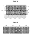
- FIG 1A illustrates a module that includes an array 101 of crystal elements and an array 102 of PMTs.
- the array 101 includes a plurality of crystal elements 103 and the array 102 includes a plurality of PMTs 104.
- This approach minimizes the number of optical interfaces and boundaries, and ensures excellent light collection.
- this design suffers from larger numbers of sensors being exposed to the light of a single scintillation event, potentially limiting the ability to process events occurring close to each other, as well as limiting the overall counting capacity.
- the second design is based upon an optically isolated block having, for example, four PMT sensors, so as to allow for simplified crystal identification.
- a block element 105 is composed of four photomultiplier tube sensors on an approximately 50mm x 50mm crystal assembly.
- the crystals extend to the very edge of the array and a relatively thick light guide is therefore often used to capture enough light from all PMTs to be able to detect the position of the event.
- a detector is then formed by arranging multiple blocks (e.g., three or four) to fill out the axial extent, and then repeating this pattern to create the overall cylinder. See the designs shown in Figures 1B and 1C .
- the advantages of this approach include greater flexibility (the detector block is potentially fully functional outside of the scanner (meaning that the detector block can be tested and calibrated separately, as opposed to the large area, continuous detector that can only be tested and calibration as part of a complete system - offering advantages for service at the customer site and for manufacturing of the scanner)) and better count capacity due to the potential parallel operation of each module.
- the disadvantages of this design are the inclusion of a large number of optical surfaces, potentially interfering with efficient light collection, and a more limited set of options for sensor coverage.
- quadrant sharing can be implemented in two ways.
- the detector is essentially continuous around the entire circumference of the ring.
- scintillator arrays 1005 of quadrant sharing modules 1004 can be placed closer if they share PMTs, thereby losing their independence.
- the modules essentially become a single continuous detector in which some PMTs 1006 are shared between modules.
- the loss of independence of the modules in the continuous quadrant sharing approach means that the detector is only fully functional once every detector module has been installed, and modules cannot be fully tested and calibrated before installation.
- the continuous quadrant sharing approach does not allow for the production and testing of fully functional independent units prior to inclusion of the units in the scanner, and also does not allow for replacement of an independent module when part of the detector fails. This is a significant practical disadvantage for the continuous quadrant sharing approach.
- a PET detector module includes an array of scintillation crystal elements and a plurality of photosensors.
- the array of the scintillation crystal elements includes a plurality of substantially optically isolated sub-arrays.
- the plurality of photosensors are arranged to cover the array of crystal elements and configured to receive light emitted from the array of crystal elements.
- the sub-arrays are optically isolated so that light emitted from an individual scintillation crystal located in a corresponding sub-array is concentrated so as to be primarily received only by those photosensors of the plurality of photosensors that cover the corresponding sub-array.
- At least one photosensor of the plurality of photosensors which receives light emitted from crystals in a first sub-array, also receives light emitted from crystals in one and only one sub-array that is adjacent to the first sub-array.
- a radiation detector in another embodiment, includes a plurality of adjacent modular detector segments.
- Each segment includes an array of scintillation crystal elements, a light guide, and reflectors.
- the light guide is arranged adjacent to the array of scintillation crystal elements.
- the reflectors are arranged around a periphery of the segment so that light produced by a scintillation event in the segment is substantially confined to the segment.
- Each segment is coupled to a plurality of photosensors, each photosensor being configured to receive light from at least one of the segments.
- a positron emission tomography (PET) scanner system in another embodiment, includes a plurality of detector modules arranged adjacent to one another to form a cylindrical detector ring.
- Each of the detector modules includes a plurality of adjacent modular detector segments.
- Each segment includes an array of scintillation crystal elements, light guide, and reflectors.
- the light guide is arranged adjacent to the array of scintillation crystal elements.
- the reflectors are arranged around a periphery of the segment so that light produced by a scintillation event in the segment is substantially confined to the segment.
- Each segment is coupled to a plurality of photosensors, each photosensor being configured to receive light at least one of the segments.
- a method of processing signals using a positron emission tomography (PET) detector module that includes an array of scintillation crystal elements, the array including a plurality of substantially optically isolated sub-arrays, and a plurality of photosensors arranged to cover the array of crystal elements and configured to receive light emitted from the array of crystal elements, includes detecting a first scintillation event from a first sub-array of the plurality of sub-arrays; detecting a second scintillation event from a second sub-array of the plurality of sub-arrays, wherein the first and second sub-arrays are separated by at least one sub-array; and analyzing first signals from each photosensor involved in the first scintillation event, and simultaneously, analyzing second signals from each photosensor involved in the second scintillation event when the first and second sub-arrays are separated by at least one sub-array.
- PET positron emission tomography
- a method of manufacturing a radiation detector module includes manufacturing a plurality of scintillation crystal sub-arrays, including two end sub-arrays and a plurality of middle sub-arrays; manufacturing a plurality of light guide pieces, including two end pieces and a plurality of middle pieces; attaching each end sub array to a corresponding one of the end pieces to form two end segments; attaching each middle sub-array to a corresponding one of the middle pieces to form a plurality of middle segments; attaching reflective material to a side surface of at least one of the middle segments; and attaching the end segments and the plurality of middle segments together to form a module base having a scintillation layer and a light guide layer.
- Figure 1D illustrates a PET scanner design 200 according to one embodiment.
- a detector ring 210 includes a number of rectangular detector modules 220.
- the detector ring 210 includes 40 detector modules 220.
- 48 modules are used to create a larger bore size for the scanner.
- a PET detector module includes an array of scintillation crystal elements and a plurality of photosensors.
- the array of the scintillation crystal elements includes a plurality of substantially optically isolated sub-arrays.
- the plurality of photosensors are arranged to cover the array of crystal elements and configured to receive light emitted from the array of crystal elements.
- the sub-arrays are optically isolated so that light emitted from an individual scintillation crystal located in a corresponding sub-array is concentrated so as to be primarily received only by those photosensors of the plurality of photosensors that cover the corresponding sub-array.
- At least one photosensor of the plurality of photosensors which receives light emitted from crystals in a first sub-array, also receives light emitted from crystals in one and only one sub-array that is adjacent to the first sub-array.
- Figure 2 illustrates a detector module design that includes a support structure 204 and a two-dimensional array of individual detector crystals 203, which absorb the gamma radiation and emit scintillation photons, which are detected by the photomultiplier tubes.
- a light guide 202 is disposed between the array of detector crystals and the photomultiplier tubes (PMTs) 201.
- each detector module includes a number of PMTs 201 of various sizes, each of which covers a plurality of detector crystals.
- Each PMT 201 produces an analog signal which rises sharply when a scintillation event occurs, and then tails off exponentially.
- the photons emitted from one detector crystal can be detected by more than one PMT 201. However, based on the analog signal produced at each PMT 201, the detector crystal corresponding to an event can be determined.
- the detector module shown in Figure 2 is narrow and long. Typically, the long axis is more than 3-4 times longer than the short axis. This design minimizes the ratio of crystals on the edge of the modules to crystals in the interior of the module and still produces a large enough multiplicity of independent modules to ensure an adequate counting capacity. Since each module is optically isolated and photosensors are not shared between adjacent modules, each module can be calibrated independently.
- the detector module arrangement of Figure 2 provides a compromise between creating as many optically independent modules as possible to maximize count rate and creating a large continuous detection surface to maximize light collection and minimize edge effects.
- Figure 2 still contains a fair amount of light sharing and light contamination along the long axis of the detector. Additionally, construction of the large structure shown in Figure 2 , with detailed optics requirement, may present some manufacturing challenges.
- one embodiment described herein is directed to a method of manufacturing the long and narrow detector module shown in Figure 2 using modular segments.
- the crystal array 203 and light guide 202 are segmented over the center line joining two PMTs.
- three types of segments are used, each segment including a crystal sub-array and a corresponding light guide sub-piece.
- One type of segment in this embodiment is an end-type segment 301, described in more detail below with respect to Figures 5 and 6 .
- the other types of segments in this embodiment are middle-type segments 302 and 303, which are also shown in Figures 5 and 6 .
- the detector module includes, for example, at least five modular detector segments.
- Each of the detector segments includes, for example, a first segment, a second segment, a third segment, a fourth segment, and fifth segment.
- the first segment includes an end-type array of scintillation crystal elements and an end-type light guide.
- the second segment includes a middle-type array of scintillation crystal elements and a first middle-type light guide.
- the third segment includes the middle-type array of scintillation crystal elements and a second middle-type light guide.
- the fourth segment includes the middle-type array of scintillation crystal elements and the first middle-type light guide.
- the fifth segment includes the end-type array of scintillation crystal elements and the end-type light guide.
- the detector module further includes reflector elements configured to substantially concentrate the light emitted from the individual scintillation crystal element in the corresponding sub-array so the emitted light is primarily received only by those photosensors of the plurality of photosensors that cover the corresponding sub-array.
- each sub-array included in the array of the scintillation crystal elements is covered by respective portions of a corresponding group of four photosensors of the plurality of photosensors.
- Light from any individual scintillation crystal located in a corresponding sub-array is concentrated so as to be primarily received only by the respective portions of the corresponding group of four photosensors.
- At least two photosensors of the plurality of photosensors, which receives light emitted from crystals in the first sub-array also receives light emitted from crystals in one and only one sub-array that is adjacent to the first sub-array.
- the detector module further includes a signal processing device configured to aggregate, for each scintillation event, output signals from each photosensor in a trigger zone of a plurality of overlapping trigger zones defined for the module, each trigger zone including a plurality of photosensors of the plurality of photosensors. At least one photosensor, which receives light from adjacent sub-arrays, belongs to two trigger zones.
- each sub-array is optically isolated by attaching reflective material 304 around each crystal sub-array shown in Figure 3 .
- Several advantages result from this.
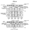
- the signals from all PMTs in a group of four are connected to form a trigger zone (i.e., the PMTs that are summed in the analog domain to generate the timing trigger signal).
- Figure 4 shows five trigger zones, with PMTs 1-4 forming a first trigger zone, PMTs 3-6 forming a second trigger zone, etc.
- Having small trigger zones is an advantage with respect to timing resolution.
- the pre-amplifier on each PMT channel adds some noise to the signal, so reducing the total number of channels in the trigger zone reduces the total noise.
- Light that spreads beyond the four-PMT region does not contribute to the timing signal.
- essentially all of the scintillation light from a gamma event is confined to a single trigger zone.
- the increased signal-to-noise ratio results in improved timing resolution. Since the boundaries of the over-lapping trigger zones align with the center of the light sensors, the boundaries (seams) of the segments must also align with the center of the light sensors to fully realize this benefit.
- two events can be processed at the same time provided that the events do not share any PMTs, which is accomplished as soon as there are one or more sub-arrays between the two events under consideration.
- the events are processed using a combination of analog and digital electronics to produce an estimate of the arrival time, the energy, and the interaction position for each gamma ray.
- the timing is derived by generating a composite timing signal by analog summation of signals from a number of PMTs. Next, a leading-edge or constant-fraction discriminator is applied to the composite signal.
- the PMTs whose signals are summed are often referred to as a "trigger zone," which may overlap or which may be kept separate. In one embodiment, the trigger zones overlap.
- the summed signal for each trigger zone usually initiates the acquisition or processing of energy and position information.
- each PMT is connected to an independent channel of electronics which typically includes a shaping filter and an analog-to-digital converter.
- the PMT signals for each PMT in the trigger zone are integrated over a pre-determined time window.
- the integrated PMT signals are then digitally summed to produce an estimate of the energy of the event, and a centroid calculation using these signals is used to estimate the interaction position.
- Modern systems include multiple corrections, often based on stored look-up tables, to further improve the timing, energy, and position estimate.
- the detector module detects a first scintillation event from a first sub-array of the plurality of sub-arrays.
- the detector module detects a second scintillation event from a second sub-array of the plurality of sub-arrays, wherein the first and second sub-arrays are separated by at least one sub-array.
- the signal processing device then analyzes first signals from each photosensor involved in the first scintillation event, and simultaneously, analyzes second signals from each photosensor involved in the second scintillation event when the first and second sub-arrays are separated by at least one sub-array.
- the signal processing device when analyzing the first signals and the second signals, determines a first position, a first energy, and a first arrival time for the first scintillation event. The signal processing device then determines a second position, a second energy, and a second arrival time for the second scintillation event.
- the light from one scintillation event will be channeled to fewer sensors, increasing the statistical quality of the detection, which results in better timing information.
- the light distribution from two events can overlap (mutual interference or pile-up), especially at high count rates, which decreases the quality of the detection.
- crystal sub-arrays and the light guide pieces for the different segments can be optically coupled (e.g., glued together) and inspected independently.
- a problem with one segment can be fixed without remanufacturing the entire detector module.
- small crystal sub-arrays are easier to manufacture and handle, which should lead to a cost reduction.
- variable sized detector modules can be created and easily maintained with the same set of sub-arrays.
- a 20 cm long detector can be manufactured using two types of crystal sub-arrays (two 12x16 end arrays and three 8x16 middle arrays) and three types of light guide sub-pieces (an end piece and two types of middle pieces), as shown in Figure 5 .
- a 32 cm detector module can be manufactured using the same sub-arrays (two 12x16 end arrays and seven 8x16 middle arrays) and the same light guide sub-pieces.
- the 32 cm detector module uses four middle pieces of the first type and three middle pieces of the second type, in addition to the two end pieces.
- Other sizes of crystal sub-arrays and other combinations or sizes of light guide pieces are possible.
- the detector module includes exactly nine modular detector segments. Further, for example, the detector module includes an odd number of middle modular detector segments and two end modular detector segments.
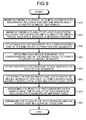
- Figure 9 illustrates the steps in a method of manufacturing a radiation detector module according to one embodiment.
- a plurality of scintillation crystal sub-arrays including two end sub-arrays and a plurality of middle sub-arrays is manufactured. See Figures 5 and 6 , for example.
- a plurality of light guide pieces including two end pieces and a plurality of middle pieces are manufactured.
- each light guide piece includes at least one recessed portion for holding portions of one or more PMTs.
- each end sub array is attached to a corresponding one of the end light guide pieces to form two end segments.
- each middle sub-array is attached to a corresponding one of the middle pieces to form a plurality of middle segments. For example, see Figures 3 , 5 , and 6 .
- step 950 reflective material is attached to side surfaces of each of the end and middle segments.
- step 960 the end segments and the plurality of middle segments are attached together, for example in the order shown in one of Figures 5 and 6 , to form a module base having a scintillation layer and a light guide layer.
- a plurality of photosensors is arranged on the module base using the recessed portions to hold the photosensors in place, wherein the plurality of photosensors can include photosensors of different sizes.
- step 980 the plurality of photosensors and the module base is arranged in the support structure 204 shown in Figure 2 .
- the step 920 may include a step of forming, in each light guide piece, at least two recessed portions for holding respective photosensors of different sizes
- the step 970 may include a step of arranging a plurality of photosensors on the module base, the plurality of photosensors including photosensors of different sizes.
- the step 920 may include a step manufacturing at least one middle piece of a first type and at least one middle piece of a second type.
- the concepts discussed above can be applied to other configurations using the rule that each sub-array needs to be connected to the smallest number of sensors necessary to perform the positioning calculation.
- the minimum number of sensors required is four for the top configuration, while the minimum number of sensors required is three for the lower two designs shown in Figure 7 .
- the dotted lines shown in Figure 7 indicate how the module is segmented, but that not all of the segments are shown.
- Figures 11A and 11B illustrate a segmented design allowing for a plurality of independent modules (as shown for example in Figure 11A ) to be placed close together with minimal gaps there between, while retaining their independence, as shown in Figure 11B .
- the gap between modules in Figure 11B is significantly smaller than the width of a photosensor, and comparable to a single crystal width or smaller, e.g., less than four mm.
- the plurality of detector modules are independent and are arranged closer to one another than the width of one of the photosensors so as to form the cylindrical detector ring. Further, the plurality of detector modules are independent and are arranged less than four mm between one another so as to form the cylindrical detector ring.
- At least one photosensor (of the plurality of photosensors in the module), which receives light emitted from crystals in a first sub-array, also receives light emitted from crystals in one and only one sub-array that is adjacent to the first sub-array.
- the photosensors are only shared in one direction and between at most two sub-arrays.
- the sensor array is substantially the same size as the crystal array, which imposes restrictions on the size of the assembly.
- the crystal array has to be substantially the size of the sensor diameter, or a little smaller to account for manufacturing and assembly tolerances.
- embodiments disclosed herein offers a cost reduction, an increase in the total amount of light available for detection, and better performance at high count rates than continuous detectors.
Landscapes
- Physics & Mathematics (AREA)
- Health & Medical Sciences (AREA)
- Spectroscopy & Molecular Physics (AREA)
- Life Sciences & Earth Sciences (AREA)
- Molecular Biology (AREA)
- High Energy & Nuclear Physics (AREA)
- General Physics & Mathematics (AREA)
- Nuclear Medicine, Radiotherapy & Molecular Imaging (AREA)
- Optics & Photonics (AREA)
- Biomedical Technology (AREA)
- Medical Informatics (AREA)
- General Health & Medical Sciences (AREA)
- Engineering & Computer Science (AREA)
- Chemical & Material Sciences (AREA)
- Crystallography & Structural Chemistry (AREA)
- Measurement Of Radiation (AREA)
- Nuclear Medicine (AREA)
Abstract
Description
- Embodiments described herein relate generally to the design of radiation detectors, such as for gamma ray detection and positron emission tomography.
- The use of gamma ray detectors in general, and positron emission tomography (PET) in particular, is growing in the field of medical imaging. In PET imaging, a radiopharmaceutical agent is introduced into an object to be imaged via injection, inhalation, or ingestion. After administration of the radiopharmaceutical, the physical and bio-molecular properties of the agent will cause it to concentrate at specific locations in the human body. The actual spatial distribution of the agent, the intensity of the region of accumulation of the agent, and the kinetics of the process from administration to eventually elimination are all factors that may have clinical significance. During this process, a positron emitter attached to the radiopharmaceutical agent will emit positrons according to the physical properties of the isotope, such as half-life, branching ratio, etc.
- The radionuclide emits positrons, and when an emitted positron collides with an electron, an annihilation event occurs, wherein the positron and electron are destroyed. Most of the time, an annihilation event produces two gamma rays (at 511 keV) traveling at substantially 180 degrees apart.
- By detecting the two gamma rays, and drawing a line between their locations, i.e., the line-of-response (LOR), one can retrieve the likely location of the original disintegration. While this process will only identify a line of possible interaction, by accumulating a large number of those lines, and through a tomographic reconstruction process, the original distribution can be estimated. In addition to the location of the two scintillation events, if accurate timing (within few hundred picoseconds) is available, a time-of-flight (TOF) calculation can add more information regarding the likely position of the event along the line. Limitations in the timing resolution of the scanner will determine the accuracy of the positioning along this line. Limitations in the determination of the location of the original scintillation events will determine the ultimate spatial resolution of the scanner, while the specific characteristics of the isotope (e.g., energy of the positron) will also contribute (via positron range and co-linearity of the two gamma rays) to the determination of the spatial resolution the specific agent.
- The above described detection process must be repeated for a large number of annihilation events. While each imaging case must be analyzed to determine how many counts (i.e., paired events) are required to support the imaging task, current practice dictates that a typical 100-cm long, FDG (fluoro-deoxyglucose) study will need to accumulate several hundred million counts. The time required to accumulate this number of counts is determined by the injected dose of the agent and the sensitivity and counting capacity of the scanner.
- PET imaging systems use detectors positioned across from one another to detect the gamma rays emitting from the object. Typically a ring of detectors is used in order to detect gamma rays coming from each angle. Thus, a PET scanner is typically substantially cylindrical to be able to capture as much radiation as possible, which should be, by definition, isotropic. Once the overall geometry of the PET scanner is known, another challenge is to arrange as much scintillating material as possible in the gamma ray paths to stop and convert as many gamma rays as possible into light. In order to be able to reconstruct the spatio-temporal distribution of the radio-isotope via tomographic reconstruction principles, each detected event will need to be characterized for its energy (i.e., amount of light generated), its location, and its timing. Most modern PET scanners are composed of several thousand individual crystals, which are arranged in modules and are used to identify the position of the scintillation event. Typically crystal elements have a cross section of roughly 4mm x 4mm. Smaller or larger dimensions and non-square sections are also possible. The length or depth of the crystal will determine how likely the gamma ray will be captured, and typically ranges from 10 to 30mm. The detector module is the main building block of the scanner.
- PET imaging relies on the conversion of gamma rays into light through fast and bright scintillation crystals. After determining the interaction position in the scintillator and time pairing of individual events, the location of the annihilation process can be recreated. These actions require very fast components - detector and electronics - and they also require excellent signal to noise ratio. With high quality electronics, the signal to noise ratio is mainly determined by the inherent Poisson statistics involved in the detection process. Detecting more photons will result in improved signal-to-noise-ratio, and, therefore, better spatial and timing resolution. No improvement in detector design and electronics can compensate for significant loss of light in the detection process. The fraction of the total amount of light collected (relative to the amount created in the scintillator) is a good measure of the efficiency of the design. So to maximize the amount of light collected, one would try to get the light sensor as close as possible to the scintillation crystal and avoid reflections and other edge effects. This would then force the arrangement to be large array detector with short distance between crystal and sensor.
- As described above, a PET imaging system is more than just a counter and, in addition to detecting the presence of a scintillation event, the system must identify its location. Conceptually, perhaps the most straightforward design to allow identification of the location of each interaction is to have a separate photosensor and data acquisition channel for each scintillator crystal. Due to constraints such as the physical size of common photosensors, the power required for each data acquisition channel, and the associated cost of these items, some form of multiplexing is usually used to reduce the number of photosensors and channels of electronics.
- By properly documenting how light is being distributed to the multiple light sensors, it is possible to assign an event location for any given set of sensor responses. Light therefore needs to be distributed to multiple sensors. In order to accomplish an adequate light distribution (so that enough sensors would detect a fraction of the light) it may be necessary to increase the thickness of the light guide or space between the crystals and the sensor. However, fast counting requires that multiple events be processed simultaneously, favoring optical isolation between scintillation events, and the creation of smaller detector blocks. These two requirements are pushing the detector design in two different directions.
- Currently available PET scanners have two main detector module designs. The first type is a large area detector in which an array of crystals that covers the entire axial extent of the cylinder is formed. Several modules are then arranged together to form a cylinder, each module being optically coupled to the next. An array of photosensors (e.g., photomultiplier tubes or PMTs) is placed on the modules and on the interfaces between modules. See the design shown in
Figure 1A , which illustrates a module that includes anarray 101 of crystal elements and anarray 102 of PMTs. Thearray 101 includes a plurality ofcrystal elements 103 and thearray 102 includes a plurality ofPMTs 104. This approach minimizes the number of optical interfaces and boundaries, and ensures excellent light collection. However, this design suffers from larger numbers of sensors being exposed to the light of a single scintillation event, potentially limiting the ability to process events occurring close to each other, as well as limiting the overall counting capacity. - The second design is based upon an optically isolated block having, for example, four PMT sensors, so as to allow for simplified crystal identification. In the design of
Figure 1B , ablock element 105 is composed of four photomultiplier tube sensors on an approximately 50mm x 50mm crystal assembly. In this approach, the crystals extend to the very edge of the array and a relatively thick light guide is therefore often used to capture enough light from all PMTs to be able to detect the position of the event. A detector is then formed by arranging multiple blocks (e.g., three or four) to fill out the axial extent, and then repeating this pattern to create the overall cylinder. See the designs shown inFigures 1B and1C . The advantages of this approach include greater flexibility (the detector block is potentially fully functional outside of the scanner (meaning that the detector block can be tested and calibrated separately, as opposed to the large area, continuous detector that can only be tested and calibration as part of a complete system - offering advantages for service at the customer site and for manufacturing of the scanner)) and better count capacity due to the potential parallel operation of each module. The disadvantages of this design are the inclusion of a large number of optical surfaces, potentially interfering with efficient light collection, and a more limited set of options for sensor coverage. - As shown in the bottom of
Figure 8 , in one design of the conventional art, an array of overlapping PMTs is arranged over small 2D crystal arrays. In this case, four quadrants from four sensors cover each crystal array. However, for this design, there is no means to manage the edges and the concept seems to be better adapted to covering large surfaces. Further, modern PET systems with ToF capabilities use mostly 1 and 1 ½ inch PMTs, which implies a large number of very small arrays. In addition, this design has no equivalent implementation in a long and narrow detector. The 1D version shown in the top ofFigure 8 , with one sensor sharing half of its surface with two adjacent sub-arrays simply does not carry enough information to perform 2D positioning. - For example, quadrant sharing can be implemented in two ways.
- In the independent module quadrant sharing approach, adjacent independent modules, such as the
module 101 shown inFigure 10A , are not optically coupled and do not share anyPMTs 1002. As shown inFigure 10B ,scintillator arrays 1003 of independentquadrant sharing modules 1001 cannot be placed closer than approximately the width of one photosensor (PMT). The large gaps between adjacent modules in the independent quadrant sharing approach are a major disadvantage of that approach. Moreover, the independent module quadrant sharing approach on a long and narrow array would be terribly inefficient and would clearly prevent close packing. - In the continuous quadrant sharing approach, as shown in
Figure 10C , the detector is essentially continuous around the entire circumference of the ring. In this approach,scintillator arrays 1005 ofquadrant sharing modules 1004 can be placed closer if they share PMTs, thereby losing their independence. In this case, the modules essentially become a single continuous detector in which somePMTs 1006 are shared between modules. The loss of independence of the modules in the continuous quadrant sharing approach means that the detector is only fully functional once every detector module has been installed, and modules cannot be fully tested and calibrated before installation. The continuous quadrant sharing approach does not allow for the production and testing of fully functional independent units prior to inclusion of the units in the scanner, and also does not allow for replacement of an independent module when part of the detector fails. This is a significant practical disadvantage for the continuous quadrant sharing approach. - A more complete appreciation of the invention and many of the attendant advantages thereof will be readily obtained as the same becomes better understood by reference to the following detailed description when considered in connection with the accompanying drawings, wherein:
-
FIGs. 1A, 1B , and1C illustrate conventional PET detector module designs in which photosensors are arranged to cover scintillation arrays;
FIG. 1D illustrates a PET scanner ring having a plurality of detector modules; -
FIG. 2 illustrates one embodiment of a detector module, which includes a support structure, a scintillator array, a light guide, and an arrangement of PMTs; -
FIG. 3 illustrates a radiation detector including a plurality of adjacent modular detector segments, each segment including a crystal array and a light guide; -
FIG. 4 illustrates trigger zones and a comparison of the light distribution for two events in segmented and non-segmented embodiments; -
FIG. 5 illustrates crystal sub-arrays and corresponding light guide pieces in a 20 cm FOV embodiment; -
FIG. 6 illustrates crystal sub-arrays and corresponding light guide pieces in a 32 cm FOV embodiment; -
FIG. 7 illustrates segmented detector modules according to alternative embodiments; -
FIG. 8 illustrates conventional detector modules; -
FIG. 9 illustrates the steps in a method of manufacturing a radiation detector module according to one embodiment; -
FIGs. 10A-10C illustrate conventional quadrant sharing designs; and -
FIGs. 11A and 11B illustrate an independent-module, continuous quadrant-sharing embodiment. - In one embodiment, a PET detector module includes an array of scintillation crystal elements and a plurality of photosensors. The array of the scintillation crystal elements includes a plurality of substantially optically isolated sub-arrays. The plurality of photosensors are arranged to cover the array of crystal elements and configured to receive light emitted from the array of crystal elements. The sub-arrays are optically isolated so that light emitted from an individual scintillation crystal located in a corresponding sub-array is concentrated so as to be primarily received only by those photosensors of the plurality of photosensors that cover the corresponding sub-array. At least one photosensor of the plurality of photosensors, which receives light emitted from crystals in a first sub-array, also receives light emitted from crystals in one and only one sub-array that is adjacent to the first sub-array.
- In another embodiment, a radiation detector includes a plurality of adjacent modular detector segments. Each segment includes an array of scintillation crystal elements, a light guide, and reflectors. The light guide is arranged adjacent to the array of scintillation crystal elements. The reflectors are arranged around a periphery of the segment so that light produced by a scintillation event in the segment is substantially confined to the segment. Each segment is coupled to a plurality of photosensors, each photosensor being configured to receive light from at least one of the segments.
- In another embodiment, a positron emission tomography (PET) scanner system includes a plurality of detector modules arranged adjacent to one another to form a cylindrical detector ring. Each of the detector modules includes a plurality of adjacent modular detector segments. Each segment includes an array of scintillation crystal elements, light guide, and reflectors. The light guide is arranged adjacent to the array of scintillation crystal elements. The reflectors are arranged around a periphery of the segment so that light produced by a scintillation event in the segment is substantially confined to the segment. Each segment is coupled to a plurality of photosensors, each photosensor being configured to receive light at least one of the segments.
- In another embodiment, a method of processing signals using a positron emission tomography (PET) detector module that includes an array of scintillation crystal elements, the array including a plurality of substantially optically isolated sub-arrays, and a plurality of photosensors arranged to cover the array of crystal elements and configured to receive light emitted from the array of crystal elements, includes detecting a first scintillation event from a first sub-array of the plurality of sub-arrays; detecting a second scintillation event from a second sub-array of the plurality of sub-arrays, wherein the first and second sub-arrays are separated by at least one sub-array; and analyzing first signals from each photosensor involved in the first scintillation event, and simultaneously, analyzing second signals from each photosensor involved in the second scintillation event when the first and second sub-arrays are separated by at least one sub-array.
- In another embodiment, a method of manufacturing a radiation detector module includes manufacturing a plurality of scintillation crystal sub-arrays, including two end sub-arrays and a plurality of middle sub-arrays; manufacturing a plurality of light guide pieces, including two end pieces and a plurality of middle pieces; attaching each end sub array to a corresponding one of the end pieces to form two end segments; attaching each middle sub-array to a corresponding one of the middle pieces to form a plurality of middle segments; attaching reflective material to a side surface of at least one of the middle segments; and attaching the end segments and the plurality of middle segments together to form a module base having a scintillation layer and a light guide layer.
- Referring now to the drawings,
Figure 1D illustrates aPET scanner design 200 according to one embodiment. As shown inFigure 1D , adetector ring 210 includes a number ofrectangular detector modules 220. According to one embodiment, thedetector ring 210 includes 40detector modules 220. In another embodiment, 48 modules are used to create a larger bore size for the scanner. - A PET detector module includes an array of scintillation crystal elements and a plurality of photosensors. The array of the scintillation crystal elements includes a plurality of substantially optically isolated sub-arrays. The plurality of photosensors are arranged to cover the array of crystal elements and configured to receive light emitted from the array of crystal elements. The sub-arrays are optically isolated so that light emitted from an individual scintillation crystal located in a corresponding sub-array is concentrated so as to be primarily received only by those photosensors of the plurality of photosensors that cover the corresponding sub-array. At least one photosensor of the plurality of photosensors, which receives light emitted from crystals in a first sub-array, also receives light emitted from crystals in one and only one sub-array that is adjacent to the first sub-array.
- For example,
Figure 2 illustrates a detector module design that includes asupport structure 204 and a two-dimensional array ofindividual detector crystals 203, which absorb the gamma radiation and emit scintillation photons, which are detected by the photomultiplier tubes. Alight guide 202 is disposed between the array of detector crystals and the photomultiplier tubes (PMTs) 201. As shown inFigure 2 , each detector module includes a number ofPMTs 201 of various sizes, each of which covers a plurality of detector crystals. EachPMT 201 produces an analog signal which rises sharply when a scintillation event occurs, and then tails off exponentially. The photons emitted from one detector crystal can be detected by more than onePMT 201. However, based on the analog signal produced at eachPMT 201, the detector crystal corresponding to an event can be determined. - The detector module shown in
Figure 2 is narrow and long. Typically, the long axis is more than 3-4 times longer than the short axis. This design minimizes the ratio of crystals on the edge of the modules to crystals in the interior of the module and still produces a large enough multiplicity of independent modules to ensure an adequate counting capacity. Since each module is optically isolated and photosensors are not shared between adjacent modules, each module can be calibrated independently. - The detector module arrangement of
Figure 2 provides a compromise between creating as many optically independent modules as possible to maximize count rate and creating a large continuous detection surface to maximize light collection and minimize edge effects. - The configuration of
Figure 2 still contains a fair amount of light sharing and light contamination along the long axis of the detector. Additionally, construction of the large structure shown inFigure 2 , with detailed optics requirement, may present some manufacturing challenges. - For example, one embodiment described herein is directed to a method of manufacturing the long and narrow detector module shown in
Figure 2 using modular segments. As shown inFigure 3 , by segmenting thecrystal array 203 andlight guide 202, better performance and easier manufacturability can be achieved. In one embodiment, thecrystal array 203 andlight guide 202 are segmented over the center line joining two PMTs. In the embodiment shown inFigure 3 , three types of segments are used, each segment including a crystal sub-array and a corresponding light guide sub-piece. One type of segment in this embodiment is an end-type segment 301, described in more detail below with respect toFigures 5 and6 . The other types of segments in this embodiment are middle-type segments Figures 5 and6 . - As described above, the detector module includes, for example, at least five modular detector segments. Each of the detector segments includes, for example, a first segment, a second segment, a third segment, a fourth segment, and fifth segment. The first segment includes an end-type array of scintillation crystal elements and an end-type light guide. The second segment includes a middle-type array of scintillation crystal elements and a first middle-type light guide. The third segment includes the middle-type array of scintillation crystal elements and a second middle-type light guide. The fourth segment includes the middle-type array of scintillation crystal elements and the first middle-type light guide. The fifth segment includes the end-type array of scintillation crystal elements and the end-type light guide.
- The detector module further includes reflector elements configured to substantially concentrate the light emitted from the individual scintillation crystal element in the corresponding sub-array so the emitted light is primarily received only by those photosensors of the plurality of photosensors that cover the corresponding sub-array.
- Further, each sub-array included in the array of the scintillation crystal elements is covered by respective portions of a corresponding group of four photosensors of the plurality of photosensors. Light from any individual scintillation crystal located in a corresponding sub-array is concentrated so as to be primarily received only by the respective portions of the corresponding group of four photosensors. At least two photosensors of the plurality of photosensors, which receives light emitted from crystals in the first sub-array, also receives light emitted from crystals in one and only one sub-array that is adjacent to the first sub-array.
- Furthermore, the detector module further includes a signal processing device configured to aggregate, for each scintillation event, output signals from each photosensor in a trigger zone of a plurality of overlapping trigger zones defined for the module, each trigger zone including a plurality of photosensors of the plurality of photosensors. At least one photosensor, which receives light from adjacent sub-arrays, belongs to two trigger zones.
- For example, in this embodiment, each sub-array is optically isolated by attaching
reflective material 304 around each crystal sub-array shown inFigure 3 . Several advantages result from this. First, light from one sub-array will stay on the same array and will decrease the overlap or contamination of adjacent sub-arrays, as discussed below with respect toFigure 4 . Second, each scintillation event will always affect only four PMTs. In this embodiment, the signals from all PMTs in a group of four are connected to form a trigger zone (i.e., the PMTs that are summed in the analog domain to generate the timing trigger signal). For example,Figure 4 shows five trigger zones, with PMTs 1-4 forming a first trigger zone, PMTs 3-6 forming a second trigger zone, etc. - Having small trigger zones, as in this embodiment, is an advantage with respect to timing resolution. For example, the pre-amplifier on each PMT channel adds some noise to the signal, so reducing the total number of channels in the trigger zone reduces the total noise. Light that spreads beyond the four-PMT region does not contribute to the timing signal. In this embodiment, essentially all of the scintillation light from a gamma event is confined to a single trigger zone. The increased signal-to-noise ratio results in improved timing resolution. Since the boundaries of the over-lapping trigger zones align with the center of the light sensors, the boundaries (seams) of the segments must also align with the center of the light sensors to fully realize this benefit.
- Moreover, two events can be processed at the same time provided that the events do not share any PMTs, which is accomplished as soon as there are one or more sub-arrays between the two events under consideration. The events are processed using a combination of analog and digital electronics to produce an estimate of the arrival time, the energy, and the interaction position for each gamma ray. In most conventional gamma ray detection systems, the timing is derived by generating a composite timing signal by analog summation of signals from a number of PMTs. Next, a leading-edge or constant-fraction discriminator is applied to the composite signal.
- The PMTs whose signals are summed are often referred to as a "trigger zone," which may overlap or which may be kept separate. In one embodiment, the trigger zones overlap. In addition to being used to derive the arrival time of an event, the summed signal for each trigger zone usually initiates the acquisition or processing of energy and position information. Generally, each PMT is connected to an independent channel of electronics which typically includes a shaping filter and an analog-to-digital converter. When the acquisition is triggered, the PMT signals for each PMT in the trigger zone are integrated over a pre-determined time window. The integrated PMT signals are then digitally summed to produce an estimate of the energy of the event, and a centroid calculation using these signals is used to estimate the interaction position. Modern systems include multiple corrections, often based on stored look-up tables, to further improve the timing, energy, and position estimate.
- As described above, in a method of processing signals using the detector module, the detector module detects a first scintillation event from a first sub-array of the plurality of sub-arrays. The detector module then detects a second scintillation event from a second sub-array of the plurality of sub-arrays, wherein the first and second sub-arrays are separated by at least one sub-array. The signal processing device then analyzes first signals from each photosensor involved in the first scintillation event, and simultaneously, analyzes second signals from each photosensor involved in the second scintillation event when the first and second sub-arrays are separated by at least one sub-array.
- Further, the signal processing device, when analyzing the first signals and the second signals, determines a first position, a first energy, and a first arrival time for the first scintillation event. The signal processing device then determines a second position, a second energy, and a second arrival time for the second scintillation event.
- Further, as illustrated in the bottom of
Figure 4 , the light from one scintillation event will be channeled to fewer sensors, increasing the statistical quality of the detection, which results in better timing information. In the non-segmented design shown in the top ofFigure 4 , the light distribution from two events can overlap (mutual interference or pile-up), especially at high count rates, which decreases the quality of the detection. - Additionally, the segmented approach of
Figure 3 provides easier and more cost-effective manufacturability. Since the crystal is by far the most expensive component of the scanner, production yield on crystal arrays should be higher since a faulty or otherwise under-performing array could be rejected with a smaller impact on cost, since the faulty array affects is only a small sub-array. - Further, the crystal sub-arrays and the light guide pieces for the different segments can be optically coupled (e.g., glued together) and inspected independently. Thus, a problem with one segment can be fixed without remanufacturing the entire detector module. In addition, small crystal sub-arrays are easier to manufacture and handle, which should lead to a cost reduction.
- Further, variable sized detector modules can be created and easily maintained with the same set of sub-arrays. For instance, a 20 cm long detector can be manufactured using two types of crystal sub-arrays (two 12x16 end arrays and three 8x16 middle arrays) and three types of light guide sub-pieces (an end piece and two types of middle pieces), as shown in
Figure 5 . In addition, as shown inFigure 6 , a 32 cm detector module can be manufactured using the same sub-arrays (two 12x16 end arrays and seven 8x16 middle arrays) and the same light guide sub-pieces. In particular, the 32 cm detector module uses four middle pieces of the first type and three middle pieces of the second type, in addition to the two end pieces. Other sizes of crystal sub-arrays and other combinations or sizes of light guide pieces are possible. - As described above, for example, The detector module includes exactly nine modular detector segments. Further, for example, the detector module includes an odd number of middle modular detector segments and two end modular detector segments.
- Again, because the crystal is an expensive component, manufacturing processes using shared components between different types of scanners and building the required proportion of each type according to live market conditions should be much more efficient.
-
Figure 9 illustrates the steps in a method of manufacturing a radiation detector module according to one embodiment. - In
step 910, a plurality of scintillation crystal sub-arrays, including two end sub-arrays and a plurality of middle sub-arrays is manufactured. SeeFigures 5 and6 , for example. - In
step 920, a plurality of light guide pieces, including two end pieces and a plurality of middle pieces are manufactured. For example, seeFigure 3 , which illustrates that each light guide piece includes at least one recessed portion for holding portions of one or more PMTs. - In
step 930, each end sub array is attached to a corresponding one of the end light guide pieces to form two end segments. - In
step 940, each middle sub-array is attached to a corresponding one of the middle pieces to form a plurality of middle segments. For example, seeFigures 3 ,5 , and6 . - In
step 950, reflective material is attached to side surfaces of each of the end and middle segments. - In
step 960, the end segments and the plurality of middle segments are attached together, for example in the order shown in one ofFigures 5 and6 , to form a module base having a scintillation layer and a light guide layer. - In
step 970, a plurality of photosensors is arranged on the module base using the recessed portions to hold the photosensors in place, wherein the plurality of photosensors can include photosensors of different sizes. - In
step 980, the plurality of photosensors and the module base is arranged in thesupport structure 204 shown inFigure 2 . - Further, for example, the
step 920 may include a step of forming, in each light guide piece, at least two recessed portions for holding respective photosensors of different sizes, and thestep 970 may include a step of arranging a plurality of photosensors on the module base, the plurality of photosensors including photosensors of different sizes. - Furthermore, for example, the
step 920 may include a step manufacturing at least one middle piece of a first type and at least one middle piece of a second type. - In alternative embodiments, the concepts discussed above can be applied to other configurations using the rule that each sub-array needs to be connected to the smallest number of sensors necessary to perform the positioning calculation. For example, as shown in
Figure 7 , the minimum number of sensors required is four for the top configuration, while the minimum number of sensors required is three for the lower two designs shown inFigure 7 . We note that the dotted lines shown inFigure 7 indicate how the module is segmented, but that not all of the segments are shown. -
Figures 11A and 11B illustrate a segmented design allowing for a plurality of independent modules (as shown for example inFigure 11A ) to be placed close together with minimal gaps there between, while retaining their independence, as shown inFigure 11B . In particular, the gap between modules inFigure 11B is significantly smaller than the width of a photosensor, and comparable to a single crystal width or smaller, e.g., less than four mm. - As described above, the plurality of detector modules are independent and are arranged closer to one another than the width of one of the photosensors so as to form the cylindrical detector ring. Further, the plurality of detector modules are independent and are arranged less than four mm between one another so as to form the cylindrical detector ring.
- This arrangement is possible because at least one photosensor (of the plurality of photosensors in the module), which receives light emitted from crystals in a first sub-array, also receives light emitted from crystals in one and only one sub-array that is adjacent to the first sub-array. Unlike the conventional quadrant sharing approach, in which a single photosensor is shared between more than two sub-arrrays (i.e., the photosensors are shared between sub-arrays spanning two orthogonal directions), in the present embodiment, the photosensors are only shared in one direction and between at most two sub-arrays.
- The arrangement shown in
Figure 11B is a practical advantage of the segmented module approach because each module can be fully tested and calibrated before installation in the scanner. Also, when a module has to be replaced, the replacement is faster because the replacement module does not have to be optically coupled to the neighboring modules and the module can be pre-calibrated prior to installation. - In one embodiment, the sensor array is substantially the same size as the crystal array, which imposes restrictions on the size of the assembly. In one embodiment, the crystal array has to be substantially the size of the sensor diameter, or a little smaller to account for manufacturing and assembly tolerances.
- As discussed above, embodiments disclosed herein offers a cost reduction, an increase in the total amount of light available for detection, and better performance at high count rates than continuous detectors.
- While certain embodiments have been described, these embodiments have been presented by way of example only, and are not intended to limit the scope of the inventions. Indeed the novel methods and systems described herein may be embodied in a variety of other forms; furthermore, various omissions, substitutions, and changes in the form of the methods and systems described herein may be made without departing from the spirit of the inventions. The accompanying claims and their equivalents are intended to cover such forms or modifications as would fall within the scope and spirit of the inventions.
It is explicitly stated that all features disclosed in the description and/or the claims are intended to be disclosed separately and independently from each other for the purpose of original disclosure as well as for the purpose of restricting the claimed invention independent of the composition of the features in the embodiments and/or the claims. It is explicitly stated that all value ranges or indications of groups of entities disclose every possible intermediate value or intermediate entity for the purpose of original disclosure as well as for the purpose of restricting the claimed invention, in particular as limits of value ranges.
Claims (15)
- A positron emission tomography (PET) detector module (220), comprising:an array (203) of scintillation crystal elements, the array including a plurality of substantially optically isolated sub-arrays (301, 302, 303); anda plurality of photosensors (201) arranged to cover the array (203) of crystal elements and configured to receive light emitted from the array (203) of crystal elements,wherein the sub-arrays (301, 302, 303) are optically isolated so that light emitted from an individual scintillation crystal located in a corresponding sub-array is concentrated so as to be primarily received only by those photosensors of the plurality of photosensors (201) that cover the corresponding sub-array; andat least one photosensor of the plurality of photosensors (201), which receives light emitted from crystals in a first sub-array, also receives light emitted from crystals in one and only one sub-array that is adjacent to the first sub-array.
- The PET detector module (220) of claim 1, wherein
each sub-array (301, 302, 303) is covered by respective portions of a corresponding group of four photosensors of the plurality of photosensors (201);
light from any individual scintillation crystal located in a corresponding sub-array is concentrated so as to be primarily received only by the respective portions of the corresponding group of four photosensors; and
at least two photosensors of the plurality of photosensors (201), which receives light emitted from crystals in the first sub-array, also receives light emitted from crystals in one and only one sub-array that is adjacent to the first sub-array. - The PET detector module (220) of claim 1 or 2, further comprising:a signal processing device configured to aggregate, for each scintillation event, output signals from each photosensor in a trigger zone of a plurality of overlapping trigger zones defined for the module (220), each trigger zone including a plurality of photosensors of the plurality of photosensors (201), wherein at least one photosensor, which receives light from adjacent sub-arrays, belongs to two trigger zones.
- The PET detector module (220) of any of claims 1 to 3, further comprising:reflector elements configured to substantially concentrate the light emitted from the individual scintillation crystal element in the corresponding sub-array so the emitted light is primarily received only by those photosensors of the plurality of photosensors (201) that cover the corresponding sub-array.
- A radiation detector (220), comprising:a plurality of adjacent modular detector segments (301, 302, 303), each segment (301, 302, 303) includingan array (203) of scintillation crystal elements;a light guide (202) arranged adjacent to the array of scintillation crystal elements; andreflectors (304) arranged around a periphery of the segment so that light produced by a scintillation event in the segment is substantially confined to the segment,wherein each segment is coupled to a plurality of photosensors (201), each photosensor (201) being configured to receive light from at least one of the segments.
- The radiation detector (220) of claim 5, wherein the detector (220) consists of five modular detector segments (301, 302, 303) including
a first segment (301) including an end-type array of scintillation crystal elements and an end-type light guide;
a second segment (302) including a middle-type array of scintillation crystal elements and a first middle-type light guide;
a third segment (303) including the middle-type array of scintillation crystal elements and a second middle-type light guide;
a fourth segment (302) including the middle-type array of scintillation crystal elements and the first middle-type light guide; and
a fifth segment (301) including the end-type array of scintillation crystal elements and the end-type light guide. - The radiation detector (220) of claim 5 or 6, wherein the detector (220) includes exactly nine modular detector segments, or wherein the detector (220) includes an odd number of middle modular detector segments (302, 303) and two end modular detector segments (301).
- A positron emission tomography (PET) scanner system (200), comprising:a plurality of detector modules (220) arranged adjacent to one another to form a cylindrical detector ring (210), wherein each of the detector modules (220) includes a radiation detector according to any of claims 5 to 7.
- The PET scanner system (200) of claim 8, wherein the plurality of detector modules (220) are independent and are arranged closer to one another than the width of one of the photosensors (201) so as to form the cylindrical detector ring (210), and/or wherein the plurality of detector modules (220) are independent and are arranged less than four mm between one another so as to form the cylindrical detector ring (210).
- A method of processing signals using a positron emission tomography (PET) detector module (220) that includes an array (203) of scintillation crystal elements, the array (203) including a plurality of substantially optically isolated sub-arrays (301, 302, 303), and a plurality of photosensors (201) arranged to cover the array (203) of crystal elements and configured to receive light emitted from the array (203) of crystal elements, the method comprising:detecting a first scintillation event from a first sub-array of the plurality of sub-arrays (301, 302, 303);detecting a second scintillation event from a second sub-array of the plurality of sub-arrays (301, 302, 303), wherein the first and second sub-arrays are separated by at least one sub-array; andanalyzing first signals from each photosensor involved in the first scintillation event, and simultaneously, analyzing second signals from each photosensor involved in the second scintillation event when the first and second sub-arrays are separated by at least one sub-array.
- The method of claim 10, wherein the analyzing step comprises:determining a first position, a first energy, and a first arrival time for the first scintillation event; anddetermining a second position, a second energy, and a second arrival time for the second scintillation event.
- A method of manufacturing a radiation detector module (220), comprising:manufacturing a plurality of scintillation crystal sub-arrays, including two end sub-arrays and a plurality of middle sub-arrays;manufacturing a plurality of light guide pieces, including two end pieces and a plurality of middle pieces;attaching each end sub array to a corresponding one of the end pieces to form two end segments (301);attaching each middle sub-array to a corresponding one of the middle pieces to form a plurality of middle segments (302, 303);attaching reflective material (304) to a side surface of at least one of the middle segments (302, 303); andattaching the end segments (301) and the plurality of middle segments (302, 303) together to form a module base having a scintillation layer (202) and a light guide layer (203).
- The method of claim 12, wherein the step of manufacturing the plurality of light guide pieces comprises forming, in each light guide piece, at least one recessed portion for holding a respective photosensor; and
the method further comprises arranging a plurality of photosensors (201) on the module base. - The method of claim 12, wherein the step of manufacturing the plurality of light guide pieces comprises forming, in each light guide piece, at least two recessed portions for holding respective photosensors of different sizes; and
the method further comprises arranging a plurality of photosensors (201) on the module base, the plurality of photosensors including photosensors of different sizes. - The method of any of claims 12 to 14, wherein the step of manufacturing the plurality of light guide pieces, including the plurality of middle pieces, comprises:manufacturing at least one middle piece of a first type and at least one middle piece of a second type.
Priority Applications (1)
| Application Number | Priority Date | Filing Date | Title |
|---|---|---|---|
| EP18178594.0A EP3399342A1 (en) | 2010-10-19 | 2011-10-11 | Positron emission tomography detector module, radiation detector, positron emission tomography scanner system, method of processing signals, and method of manufacturing radiation detector module |
Applications Claiming Priority (2)
| Application Number | Priority Date | Filing Date | Title |
|---|---|---|---|
| US12/907,092 US8357903B2 (en) | 2010-10-19 | 2010-10-19 | Segmented detector array |
| JP2011210687A JP6062144B2 (en) | 2010-10-19 | 2011-09-27 | PET detector module, radiation detector, PET scanner system, signal processing method, and method of manufacturing radiation detector module |
Related Child Applications (2)
| Application Number | Title | Priority Date | Filing Date |
|---|---|---|---|
| EP18178594.0A Division-Into EP3399342A1 (en) | 2010-10-19 | 2011-10-11 | Positron emission tomography detector module, radiation detector, positron emission tomography scanner system, method of processing signals, and method of manufacturing radiation detector module |
| EP18178594.0A Division EP3399342A1 (en) | 2010-10-19 | 2011-10-11 | Positron emission tomography detector module, radiation detector, positron emission tomography scanner system, method of processing signals, and method of manufacturing radiation detector module |
Publications (3)
| Publication Number | Publication Date |
|---|---|
| EP2461183A2 true EP2461183A2 (en) | 2012-06-06 |
| EP2461183A3 EP2461183A3 (en) | 2014-05-21 |
| EP2461183B1 EP2461183B1 (en) | 2018-10-03 |
Family
ID=44763991
Family Applications (2)
| Application Number | Title | Priority Date | Filing Date |
|---|---|---|---|
| EP11184684.6A Active EP2461183B1 (en) | 2010-10-19 | 2011-10-11 | Positron emission tomography detector module, radiation detector, positron emission tomography scanner system, method of processing signals, and method of manufacturing radiation detector module |
| EP18178594.0A Withdrawn EP3399342A1 (en) | 2010-10-19 | 2011-10-11 | Positron emission tomography detector module, radiation detector, positron emission tomography scanner system, method of processing signals, and method of manufacturing radiation detector module |
Family Applications After (1)
| Application Number | Title | Priority Date | Filing Date |
|---|---|---|---|
| EP18178594.0A Withdrawn EP3399342A1 (en) | 2010-10-19 | 2011-10-11 | Positron emission tomography detector module, radiation detector, positron emission tomography scanner system, method of processing signals, and method of manufacturing radiation detector module |
Country Status (2)
| Country | Link |
|---|---|
| EP (2) | EP2461183B1 (en) |
| CN (1) | CN102455432B (en) |
Cited By (4)
| Publication number | Priority date | Publication date | Assignee | Title |
|---|---|---|---|---|
| EP3214465A4 (en) * | 2014-10-30 | 2017-11-15 | Shimadzu Corporation | Radiation detector |
| CN111226140A (en) * | 2017-10-19 | 2020-06-02 | 克罗梅克集团公开有限责任公司 | Modular Gamma Imaging Device |
| CN113534233A (en) * | 2020-04-22 | 2021-10-22 | 通用电气精准医疗有限责任公司 | Systems and methods for scintillators with reflective inserts |
| CN116507944A (en) * | 2020-12-25 | 2023-07-28 | 东丽株式会社 | Scintillator panel, radiation detector, radiation inspection device, and method for manufacturing scintillator panel |
Families Citing this family (6)
| Publication number | Priority date | Publication date | Assignee | Title |
|---|---|---|---|---|
| CN103033840B (en) * | 2012-12-24 | 2015-11-18 | 中国电子科技集团公司第二十六研究所 | A kind of PET machine crystal array assemble method |
| CN103110424B (en) * | 2013-02-06 | 2014-12-10 | 江苏中惠医疗科技股份有限公司 | Detecting set of nuclear medicine detector used for positron emission tomography |
| CN103549966B (en) * | 2013-10-15 | 2016-07-27 | 沈阳东软医疗系统有限公司 | The positioner of pet detector module, submodule and photodetector |
| CN104814754A (en) * | 2015-04-01 | 2015-08-05 | 王有彬 | Positron emission neurotomography device |
| JP6451862B2 (en) * | 2015-09-17 | 2019-01-16 | 株式会社島津製作所 | Information processing apparatus, radiation detector, radiation imaging apparatus, and program |
| EP4208739A4 (en) | 2020-09-02 | 2024-10-02 | The Research Foundation for The State University of New York | CONICAL SCINTILLATOR CRYSTAL MODULES AND METHODS OF USE THEREOF |
Family Cites Families (16)
| Publication number | Priority date | Publication date | Assignee | Title |
|---|---|---|---|---|
| US4563582A (en) * | 1984-05-24 | 1986-01-07 | Clayton Foundation For Research | Positron emission tomography camera |
| US5032728A (en) * | 1988-11-09 | 1991-07-16 | The University Of Iowa Research Foundation | Single photon emission computed tomography system |
| JPH05126957A (en) * | 1991-11-06 | 1993-05-25 | Hitachi Medical Corp | Poligonal scintillation camera type position ct device |
| US5210420A (en) * | 1991-12-19 | 1993-05-11 | Positron Corporation | Positron emission tomography scanner |
| US5319204A (en) * | 1992-05-13 | 1994-06-07 | Board Of Regents, The University Of Texas System | Positron emission tomography camera with quadrant-sharing photomultipliers and cross-coupled scintillating crystals |
| US6936822B2 (en) * | 1997-05-07 | 2005-08-30 | Board Of Regents, The University Of Texas System | Method and apparatus to prevent signal pile-up |
| JP2002207080A (en) * | 2001-01-10 | 2002-07-26 | Shimadzu Corp | Radiation detector |
| JP2002267755A (en) * | 2001-03-09 | 2002-09-18 | Shimadzu Corp | Nuclear medicine imaging equipment |
| WO2002082122A2 (en) * | 2001-04-03 | 2002-10-17 | Saint Gobain Ceramics And Plastics, Inc. | Method and system for determining the energy and position information from scintillation detector |
| US7180074B1 (en) * | 2001-06-27 | 2007-02-20 | Crosetto Dario B | Method and apparatus for whole-body, three-dimensional, dynamic PET/CT examination |
| CA2474450A1 (en) * | 2002-02-01 | 2003-08-07 | Board Of Regents, The University Of Texas System | Asymmetrically placed cross-coupled scintillation crystals |
| US7238946B2 (en) * | 2003-06-27 | 2007-07-03 | Siemens Medical Solutions Usa, Inc. | Nuclear imaging system using scintillation bar detectors and method for event position calculation using the same |
| US7301153B2 (en) * | 2006-03-23 | 2007-11-27 | Siemens Medical Solutions Usa, Inc. | Photo sensor panel for high resolution PET |
| US20080075342A1 (en) * | 2006-09-27 | 2008-03-27 | Lazuka David M | Pet scanner with digital trigger |
| US20100012846A1 (en) * | 2007-07-31 | 2010-01-21 | Yu Wang | Novel scintillation detector array and associate signal processing method for gamma ray detection with encoding the energy, position, and time coordinaties of the interaction |
| CN101839991B (en) * | 2010-05-06 | 2013-06-12 | 清华大学 | Oblique arrangement type high-energy ray detector of composite photosensor |
-
2011
- 2011-10-11 EP EP11184684.6A patent/EP2461183B1/en active Active
- 2011-10-11 EP EP18178594.0A patent/EP3399342A1/en not_active Withdrawn
- 2011-10-19 CN CN201110326692.5A patent/CN102455432B/en active Active
Non-Patent Citations (1)
| Title |
|---|
| None |
Cited By (5)
| Publication number | Priority date | Publication date | Assignee | Title |
|---|---|---|---|---|
| EP3214465A4 (en) * | 2014-10-30 | 2017-11-15 | Shimadzu Corporation | Radiation detector |
| CN111226140A (en) * | 2017-10-19 | 2020-06-02 | 克罗梅克集团公开有限责任公司 | Modular Gamma Imaging Device |
| CN111226140B (en) * | 2017-10-19 | 2024-04-12 | 克罗梅克集团公开有限责任公司 | Modularized gamma imaging equipment |
| CN113534233A (en) * | 2020-04-22 | 2021-10-22 | 通用电气精准医疗有限责任公司 | Systems and methods for scintillators with reflective inserts |
| CN116507944A (en) * | 2020-12-25 | 2023-07-28 | 东丽株式会社 | Scintillator panel, radiation detector, radiation inspection device, and method for manufacturing scintillator panel |
Also Published As
| Publication number | Publication date |
|---|---|
| EP2461183A3 (en) | 2014-05-21 |
| EP2461183B1 (en) | 2018-10-03 |
| CN102455432B (en) | 2014-11-12 |
| CN102455432A (en) | 2012-05-16 |
| EP3399342A1 (en) | 2018-11-07 |
Similar Documents
| Publication | Publication Date | Title |
|---|---|---|
| US8357903B2 (en) | Segmented detector array | |
| EP2461183B1 (en) | Positron emission tomography detector module, radiation detector, positron emission tomography scanner system, method of processing signals, and method of manufacturing radiation detector module | |
| US9335425B2 (en) | Modelling of ToF-DOI detector arrays | |
| US8791514B2 (en) | Providing variable cell density and sizes in a radiation detector | |
| US8143583B2 (en) | Positron emission tomography detector elements using different sizes of photomultiplier tubes | |
| US9182506B2 (en) | Methods and systems for signal communication in gamma ray detectors | |
| US20100012846A1 (en) | Novel scintillation detector array and associate signal processing method for gamma ray detection with encoding the energy, position, and time coordinaties of the interaction | |
| US8937285B2 (en) | Methods and systems for signal communication in gamma ray detectors | |
| US8188439B2 (en) | Gamma ray detector elements with variable light guide thickness | |
| US20220179106A1 (en) | Panel Radiation Detector | |
| US6858849B2 (en) | PET apparatus | |
| CN102073058B (en) | Gamma ray detection module with variable light guide thickness | |
| US9207334B1 (en) | Methods and systems for a light sensor in gamma ray detectors | |
| CN102023307B (en) | PET detector module and PET scanner system | |
| Goertzen et al. | PET instrumentation | |
| Ott | Solid state and other detectors |
Legal Events
| Date | Code | Title | Description |
|---|---|---|---|
| PUAI | Public reference made under article 153(3) epc to a published international application that has entered the european phase |
Free format text: ORIGINAL CODE: 0009012 |
|
| 17P | Request for examination filed |
Effective date: 20111011 |
|
| AK | Designated contracting states |
Kind code of ref document: A2 Designated state(s): AL AT BE BG CH CY CZ DE DK EE ES FI FR GB GR HR HU IE IS IT LI LT LU LV MC MK MT NL NO PL PT RO RS SE SI SK SM TR |
|
| AX | Request for extension of the european patent |
Extension state: BA ME |
|
| RIC1 | Information provided on ipc code assigned before grant |
Ipc: G01T 1/202 20060101ALI20131218BHEP Ipc: G01T 1/164 20060101AFI20131218BHEP Ipc: G01T 1/29 20060101ALI20131218BHEP |
|
| PUAL | Search report despatched |
Free format text: ORIGINAL CODE: 0009013 |
|
| AK | Designated contracting states |
Kind code of ref document: A3 Designated state(s): AL AT BE BG CH CY CZ DE DK EE ES FI FR GB GR HR HU IE IS IT LI LT LU LV MC MK MT NL NO PL PT RO RS SE SI SK SM TR |
|
| AX | Request for extension of the european patent |
Extension state: BA ME |
|
| RIC1 | Information provided on ipc code assigned before grant |
Ipc: G01T 1/202 20060101ALI20140414BHEP Ipc: G01T 1/164 20060101AFI20140414BHEP Ipc: G01T 1/29 20060101ALI20140414BHEP |
|
| RAP1 | Party data changed (applicant data changed or rights of an application transferred) |
Owner name: TOSHIBA MEDICAL SYSTEMS CORPORATION |
|
| STAA | Information on the status of an ep patent application or granted ep patent |
Free format text: STATUS: EXAMINATION IS IN PROGRESS |
|
| 17Q | First examination report despatched |
Effective date: 20170327 |
|
| GRAP | Despatch of communication of intention to grant a patent |
Free format text: ORIGINAL CODE: EPIDOSNIGR1 |
|
| STAA | Information on the status of an ep patent application or granted ep patent |
Free format text: STATUS: GRANT OF PATENT IS INTENDED |
|
| INTG | Intention to grant announced |
Effective date: 20180220 |
|
| GRAS | Grant fee paid |
Free format text: ORIGINAL CODE: EPIDOSNIGR3 |
|
| GRAJ | Information related to disapproval of communication of intention to grant by the applicant or resumption of examination proceedings by the epo deleted |
Free format text: ORIGINAL CODE: EPIDOSDIGR1 |
|
| GRAL | Information related to payment of fee for publishing/printing deleted |
Free format text: ORIGINAL CODE: EPIDOSDIGR3 |
|
| STAA | Information on the status of an ep patent application or granted ep patent |
Free format text: STATUS: EXAMINATION IS IN PROGRESS |
|
| GRAR | Information related to intention to grant a patent recorded |
Free format text: ORIGINAL CODE: EPIDOSNIGR71 |
|
| STAA | Information on the status of an ep patent application or granted ep patent |
Free format text: STATUS: GRANT OF PATENT IS INTENDED |
|
| INTC | Intention to grant announced (deleted) | ||
| INTG | Intention to grant announced |
Effective date: 20180725 |
|
| GRAA | (expected) grant |
Free format text: ORIGINAL CODE: 0009210 |
|
| STAA | Information on the status of an ep patent application or granted ep patent |
Free format text: STATUS: THE PATENT HAS BEEN GRANTED |
|
| AK | Designated contracting states |
Kind code of ref document: B1 Designated state(s): AL AT BE BG CH CY CZ DE DK EE ES FI FR GB GR HR HU IE IS IT LI LT LU LV MC MK MT NL NO PL PT RO RS SE SI SK SM TR |
|
| REG | Reference to a national code |
Ref country code: GB Ref legal event code: FG4D |
|
| REG | Reference to a national code |
Ref country code: CH Ref legal event code: EP Ref country code: AT Ref legal event code: REF Ref document number: 1049219 Country of ref document: AT Kind code of ref document: T Effective date: 20181015 |
|
| REG | Reference to a national code |
Ref country code: DE Ref legal event code: R096 Ref document number: 602011052508 Country of ref document: DE Ref country code: IE Ref legal event code: FG4D Ref country code: NL Ref legal event code: FP |
|
| REG | Reference to a national code |
Ref country code: LT Ref legal event code: MG4D |
|
| REG | Reference to a national code |
Ref country code: AT Ref legal event code: MK05 Ref document number: 1049219 Country of ref document: AT Kind code of ref document: T Effective date: 20181003 |
|
| PG25 | Lapsed in a contracting state [announced via postgrant information from national office to epo] |
Ref country code: CZ Free format text: LAPSE BECAUSE OF FAILURE TO SUBMIT A TRANSLATION OF THE DESCRIPTION OR TO PAY THE FEE WITHIN THE PRESCRIBED TIME-LIMIT Effective date: 20181003 Ref country code: FI Free format text: LAPSE BECAUSE OF FAILURE TO SUBMIT A TRANSLATION OF THE DESCRIPTION OR TO PAY THE FEE WITHIN THE PRESCRIBED TIME-LIMIT Effective date: 20181003 Ref country code: PL Free format text: LAPSE BECAUSE OF FAILURE TO SUBMIT A TRANSLATION OF THE DESCRIPTION OR TO PAY THE FEE WITHIN THE PRESCRIBED TIME-LIMIT Effective date: 20181003 Ref country code: LT Free format text: LAPSE BECAUSE OF FAILURE TO SUBMIT A TRANSLATION OF THE DESCRIPTION OR TO PAY THE FEE WITHIN THE PRESCRIBED TIME-LIMIT Effective date: 20181003 Ref country code: HR Free format text: LAPSE BECAUSE OF FAILURE TO SUBMIT A TRANSLATION OF THE DESCRIPTION OR TO PAY THE FEE WITHIN THE PRESCRIBED TIME-LIMIT Effective date: 20181003 Ref country code: NO Free format text: LAPSE BECAUSE OF FAILURE TO SUBMIT A TRANSLATION OF THE DESCRIPTION OR TO PAY THE FEE WITHIN THE PRESCRIBED TIME-LIMIT Effective date: 20190103 Ref country code: AT Free format text: LAPSE BECAUSE OF FAILURE TO SUBMIT A TRANSLATION OF THE DESCRIPTION OR TO PAY THE FEE WITHIN THE PRESCRIBED TIME-LIMIT Effective date: 20181003 Ref country code: LV Free format text: LAPSE BECAUSE OF FAILURE TO SUBMIT A TRANSLATION OF THE DESCRIPTION OR TO PAY THE FEE WITHIN THE PRESCRIBED TIME-LIMIT Effective date: 20181003 Ref country code: IS Free format text: LAPSE BECAUSE OF FAILURE TO SUBMIT A TRANSLATION OF THE DESCRIPTION OR TO PAY THE FEE WITHIN THE PRESCRIBED TIME-LIMIT Effective date: 20190203 Ref country code: BG Free format text: LAPSE BECAUSE OF FAILURE TO SUBMIT A TRANSLATION OF THE DESCRIPTION OR TO PAY THE FEE WITHIN THE PRESCRIBED TIME-LIMIT Effective date: 20190103 Ref country code: ES Free format text: LAPSE BECAUSE OF FAILURE TO SUBMIT A TRANSLATION OF THE DESCRIPTION OR TO PAY THE FEE WITHIN THE PRESCRIBED TIME-LIMIT Effective date: 20181003 |
|
| PG25 | Lapsed in a contracting state [announced via postgrant information from national office to epo] |
Ref country code: AL Free format text: LAPSE BECAUSE OF FAILURE TO SUBMIT A TRANSLATION OF THE DESCRIPTION OR TO PAY THE FEE WITHIN THE PRESCRIBED TIME-LIMIT Effective date: 20181003 Ref country code: SE Free format text: LAPSE BECAUSE OF FAILURE TO SUBMIT A TRANSLATION OF THE DESCRIPTION OR TO PAY THE FEE WITHIN THE PRESCRIBED TIME-LIMIT Effective date: 20181003 Ref country code: PT Free format text: LAPSE BECAUSE OF FAILURE TO SUBMIT A TRANSLATION OF THE DESCRIPTION OR TO PAY THE FEE WITHIN THE PRESCRIBED TIME-LIMIT Effective date: 20190203 Ref country code: GR Free format text: LAPSE BECAUSE OF FAILURE TO SUBMIT A TRANSLATION OF THE DESCRIPTION OR TO PAY THE FEE WITHIN THE PRESCRIBED TIME-LIMIT Effective date: 20190104 Ref country code: RS Free format text: LAPSE BECAUSE OF FAILURE TO SUBMIT A TRANSLATION OF THE DESCRIPTION OR TO PAY THE FEE WITHIN THE PRESCRIBED TIME-LIMIT Effective date: 20181003 |
|
| REG | Reference to a national code |
Ref country code: CH Ref legal event code: PL |
|
| REG | Reference to a national code |
Ref country code: BE Ref legal event code: MM Effective date: 20181031 |
|
| PG25 | Lapsed in a contracting state [announced via postgrant information from national office to epo] |
Ref country code: LU Free format text: LAPSE BECAUSE OF NON-PAYMENT OF DUE FEES Effective date: 20181011 |
|
| REG | Reference to a national code |
Ref country code: DE Ref legal event code: R097 Ref document number: 602011052508 Country of ref document: DE |
|
| REG | Reference to a national code |
Ref country code: IE Ref legal event code: MM4A |
|
| PG25 | Lapsed in a contracting state [announced via postgrant information from national office to epo] |
Ref country code: IT Free format text: LAPSE BECAUSE OF FAILURE TO SUBMIT A TRANSLATION OF THE DESCRIPTION OR TO PAY THE FEE WITHIN THE PRESCRIBED TIME-LIMIT Effective date: 20181003 Ref country code: DK Free format text: LAPSE BECAUSE OF FAILURE TO SUBMIT A TRANSLATION OF THE DESCRIPTION OR TO PAY THE FEE WITHIN THE PRESCRIBED TIME-LIMIT Effective date: 20181003 |
|
| PLBE | No opposition filed within time limit |
Free format text: ORIGINAL CODE: 0009261 |
|
| STAA | Information on the status of an ep patent application or granted ep patent |
Free format text: STATUS: NO OPPOSITION FILED WITHIN TIME LIMIT |
|
| PG25 | Lapsed in a contracting state [announced via postgrant information from national office to epo] |
Ref country code: SM Free format text: LAPSE BECAUSE OF FAILURE TO SUBMIT A TRANSLATION OF THE DESCRIPTION OR TO PAY THE FEE WITHIN THE PRESCRIBED TIME-LIMIT Effective date: 20181003 Ref country code: EE Free format text: LAPSE BECAUSE OF FAILURE TO SUBMIT A TRANSLATION OF THE DESCRIPTION OR TO PAY THE FEE WITHIN THE PRESCRIBED TIME-LIMIT Effective date: 20181003 Ref country code: BE Free format text: LAPSE BECAUSE OF NON-PAYMENT OF DUE FEES Effective date: 20181031 Ref country code: SK Free format text: LAPSE BECAUSE OF FAILURE TO SUBMIT A TRANSLATION OF THE DESCRIPTION OR TO PAY THE FEE WITHIN THE PRESCRIBED TIME-LIMIT Effective date: 20181003 Ref country code: LI Free format text: LAPSE BECAUSE OF NON-PAYMENT OF DUE FEES Effective date: 20181031 Ref country code: MC Free format text: LAPSE BECAUSE OF FAILURE TO SUBMIT A TRANSLATION OF THE DESCRIPTION OR TO PAY THE FEE WITHIN THE PRESCRIBED TIME-LIMIT Effective date: 20181003 Ref country code: CH Free format text: LAPSE BECAUSE OF NON-PAYMENT OF DUE FEES Effective date: 20181031 Ref country code: RO Free format text: LAPSE BECAUSE OF FAILURE TO SUBMIT A TRANSLATION OF THE DESCRIPTION OR TO PAY THE FEE WITHIN THE PRESCRIBED TIME-LIMIT Effective date: 20181003 |
|
| 26N | No opposition filed |
Effective date: 20190704 |
|
| GBPC | Gb: european patent ceased through non-payment of renewal fee |
Effective date: 20190103 |
|
| PG25 | Lapsed in a contracting state [announced via postgrant information from national office to epo] |
Ref country code: IE Free format text: LAPSE BECAUSE OF NON-PAYMENT OF DUE FEES Effective date: 20181011 Ref country code: FR Free format text: LAPSE BECAUSE OF NON-PAYMENT OF DUE FEES Effective date: 20181203 Ref country code: SI Free format text: LAPSE BECAUSE OF FAILURE TO SUBMIT A TRANSLATION OF THE DESCRIPTION OR TO PAY THE FEE WITHIN THE PRESCRIBED TIME-LIMIT Effective date: 20181003 |
|
| PG25 | Lapsed in a contracting state [announced via postgrant information from national office to epo] |
Ref country code: GB Free format text: LAPSE BECAUSE OF NON-PAYMENT OF DUE FEES Effective date: 20190103 |
|
| PG25 | Lapsed in a contracting state [announced via postgrant information from national office to epo] |
Ref country code: MT Free format text: LAPSE BECAUSE OF NON-PAYMENT OF DUE FEES Effective date: 20181011 |
|
| PG25 | Lapsed in a contracting state [announced via postgrant information from national office to epo] |
Ref country code: TR Free format text: LAPSE BECAUSE OF FAILURE TO SUBMIT A TRANSLATION OF THE DESCRIPTION OR TO PAY THE FEE WITHIN THE PRESCRIBED TIME-LIMIT Effective date: 20181003 |
|
| PG25 | Lapsed in a contracting state [announced via postgrant information from national office to epo] |
Ref country code: MK Free format text: LAPSE BECAUSE OF NON-PAYMENT OF DUE FEES Effective date: 20181003 Ref country code: HU Free format text: LAPSE BECAUSE OF FAILURE TO SUBMIT A TRANSLATION OF THE DESCRIPTION OR TO PAY THE FEE WITHIN THE PRESCRIBED TIME-LIMIT; INVALID AB INITIO Effective date: 20111011 Ref country code: CY Free format text: LAPSE BECAUSE OF FAILURE TO SUBMIT A TRANSLATION OF THE DESCRIPTION OR TO PAY THE FEE WITHIN THE PRESCRIBED TIME-LIMIT Effective date: 20181003 |
|
| PGFP | Annual fee paid to national office [announced via postgrant information from national office to epo] |
Ref country code: NL Payment date: 20250826 Year of fee payment: 15 |
|
| PGFP | Annual fee paid to national office [announced via postgrant information from national office to epo] |
Ref country code: DE Payment date: 20250827 Year of fee payment: 15 |