EP2461146B1 - Sensor assembly and sensor module - Google Patents
Sensor assembly and sensor module Download PDFInfo
- Publication number
- EP2461146B1 EP2461146B1 EP10818751.9A EP10818751A EP2461146B1 EP 2461146 B1 EP2461146 B1 EP 2461146B1 EP 10818751 A EP10818751 A EP 10818751A EP 2461146 B1 EP2461146 B1 EP 2461146B1
- Authority
- EP
- European Patent Office
- Prior art keywords
- sensor
- thin film
- film
- packaging bag
- sensor element
- Prior art date
- Legal status (The legal status is an assumption and is not a legal conclusion. Google has not performed a legal analysis and makes no representation as to the accuracy of the status listed.)
- Not-in-force
Links
Images


Classifications
-
- G—PHYSICS
- G01—MEASURING; TESTING
- G01L—MEASURING FORCE, STRESS, TORQUE, WORK, MECHANICAL POWER, MECHANICAL EFFICIENCY, OR FLUID PRESSURE
- G01L1/00—Measuring force or stress, in general
- G01L1/20—Measuring force or stress, in general by measuring variations in ohmic resistance of solid materials or of electrically-conductive fluids; by making use of electrokinetic cells, i.e. liquid-containing cells wherein an electrical potential is produced or varied upon the application of stress
Definitions
- the present invention relates to a sensor assembly having a flexible sensor element that uses a polymer material. More specifically, the present invention relates to a sensor assembly having a sensor component such as a sensor element or the like that is less likely to deteriorate and is superior in durability.
- a load sensor having an elastomeric sensor thin film for example, see Patent Documents 2 and 3.
- a load sensor disclosed in Patent Document 2 a sensor thin film is formed in which conductive filler is filled in elastomer of a parent material at a predetermined state. According to this load sensor, based on a change in electrical resistance caused when the sensor thin film elastically deforms, an input load can be detected.
- a load sensor disclosed in Patent Document 3 is a capacitance-type sensor, which includes an elastomeric dielectric film and a pair of electrodes arranged sandwiching the dielectric film. According to this load sensor, based on a change in capacitance between the pair of electrodes, an input load can be detected.
- JP 5 281664 A discloses a packaging material for photographic sensitive material including a heat resistant flexible sheet, a film layer and a metallic layer disposed between the heat resistant flexible sheet and the film layer.
- a load sensor can be used in a state housed in a resin case.
- influence of moisture and oxygen with respect to a component cannot be completely eliminated.
- a sensor assembly is defined in Claim 1 and a sensor module is defined in Claim 6.
- the sensor element has the wiring unit connected to the electrical circuit.
- the wiring unit is led out from the opening of the exterior packaging bag and is connected to the electrical circuit.
- the wiring unit is housed inside the case body of the circuit case. For this reason, the wiring unit can be protected from an impact and the like.
- the packing member By using the packing member, the opening of the exterior packaging bag can be easily sealed and the sensor assembly can be installed on the circuit case.
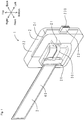
- Fig. 1 illustrates a perspective view of the sensor module according to the present embodiment.
- Fig. 2 illustrates an exploded perspective view of the sensor module.
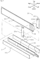
- Fig. 3 illustrates an exploded perspective view of a sensor assembly in the sensor module. In Figs. 1 - 3 , transparently visible portions are illustrated using thin lines.
- a sensor module 1 includes a circuit case 2 and a sensor assembly 3.
- the sensor module 1 is installed on a surface (front surface) of a front bumper of a vehicle (not shown in the drawings). Therefore, directions in the drawings are defined relative to a traveling direction of the vehicle.
- a load is input to the sensor assembly 3 from the front.
- the circuit case 2 includes a case body 22, a packing member 20, a connector 21, an external connection connector 23, and a circuit substrate 24.
- the case body 22 is made of resin, and has a box-like shape. As Fig. 2 illustrates, on the front surface of the case body 22, an assembly mounting opening 220 is provided opening toward the right. The assembly mounting opening 220 is in communication with inside and outside of the case body 22.
- the packing member 20 is made of resin.
- the packing member 20 has a front side securing member 20a and a rear side securing member 20b.
- the front side securing member 20a has a rectangular plate-like shape.
- a pair of recesses 200a and 201a are formed.
- the rear side securing member 20b has a rectangular plate-like shape.
- a pair of projections 200b and 201b are formed on two ends in the up-down direction on the front surface of the rear side securing member 20b.
- the circuit substrate 24 is housed inside the case body 22.
- the circuit substrate 24 is arranged in contact with a back wall of the case body 22.
- the connector 21 connects to the circuit substrate 24. Further, the connector 21 connects to the wiring unit 301 of the sensor assembly 3 inside the case body 22.
- the external connection connector 23 is penetratingly provided on a left wall of the case body 22.
- the external connection connector 23 has a terminal 230.
- the external connection connector 23 connects to the circuit substrate 24 inside the case body 22. Further, the external connection connector 23 connects to an occupant protection ECU (electronic control unit, not shown in the drawings) arranged outside the case body 22. That is, the wiring unit 301 of the sensor assembly 3 connects to the occupant protection ECU on the outside via the connector 21, the circuit substrate 24, and the external connection connector 23.
- the sensor assembly 3 is explained in detail.
- the sensor assembly 3 includes a sensor element 30 and an exterior packaging bag 40.
- the sensor element 30 has a body unit 300 and the wiring unit 301.
- the body unit 300 has a sensor thin film 32, which will be described later.
- the body unit 300 detects a load.
- the body unit 300 is enclosed inside the exterior packaging bag 40.
- the wiring unit 301 has wirings 34R and 34L, which will be described later.
- the wiring unit 301 projects out from the exterior packaging bag 40 toward the left side.
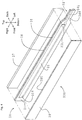
- Fig. 4 illustrates an exploded perspective view of the sensor element.
- Fig. 5 illustrates a cross-section view in a transverse direction in Fig. 4 near an electrode on the left side.
- a constraining plate and an insulation film are transparently illustrated.
- transparently visible portions are illustrated using thin lines.
- the body unit 300 of the sensor element 30 includes a constraining plate 31, the sensor thin film 32, electrodes 33R and 33L, the wirings 34R and 34L, an insulation film 35, a cover film 36, an elastic plate 37, and a load transmitting plate 38.
- the sensor thin film 32, the electrodes 33R and 33L, the wirings 34R and 34L, the insulation film 35, and the cover film 36 are all formed on the rear side of the constraining plate 31 by using a screen printing method.
- the constraining plate 31 is made of polyethylene terephthalate (PET), and has a belt-like shape extending in the left-right direction.
- PET polyethylene terephthalate
- the electrodes 33R and 33L have a square shape, and are formed on the rear surface of the constraining plate 31.
- the electrodes 33R and 33L are interposed between the constraining plate 31 and the sensor thin film 32.
- the electrode 33R is arranged on the right end of the sensor thin film 32, and the electrode 33L is arranged on the left end of the sensor thin film 32.
- the wirings 34R and 34L are formed on the rear surface of the constraining plate 31.
- the wiring 34R is connected to the electrode 33R, and the wiring 34L is connected to the electrode 33L.
- the electrodes 33R and 33L and the wirings 34R and 34L are all formed from silver paste.
- the insulation film 35 is made of acrylic resin, and has a belt-like shape extending in the left-right direction.
- the insulation film 35 covers the rear surface of the constraining plate 31 in a state excluding the electrodes 33R and 33L.
- the constraining plate 31 and the insulation film 35 are included in a base material in the present invention.
- the sensor thin film 32 has a belt-like shape extending in the left-right direction.
- the sensor thin film 32 has a film thickness of about 250 ⁇ m.
- the sensor thin film 32 is arranged on the rear surface of the constraining plate 31, more specifically, on the rear surface of the electrodes 33R and 33L and the insulation film 35.
- the sensor thin film 32 is formed in which carbon beads (conductive filler) are filled in epoxy resin. The filling rate of the carbon beads is about 45% by volume when the volume of the sensor thin film 32 is 100% by volume.
- the cover film 36 is made of acrylic rubber, and has a belt-like shape extending in the left-right direction.
- the cover film 36 covers the rear surfaces of the insulation film 35 and the sensor thin film 32.
- the elastic plate 37 is made of acrylic rubber, and has a flat plate-like shape extending in the left-right direction.
- the elastic plate 37 has a thickness of about 3 mm.
- the elastic plate 37 has a width (length in the up-down direction) of about the same as that of the constraining plate 31. Further, the elastic plate 37 has a length (length in the left-right direction) of about the same as that of the body unit 300.
- the elastic plate 37 is arranged on the rear side of the constraining plate 31. The elastic plate 37 and the cover film 36 are bonded together.
- the load transmitting plate 38 is made of an acrylonitrile-butadiene-styrene (ABS) resin, and has a flat plate-like shape extending in the left-right direction.
- the load transmitting plate 38 has dimensions of about the same as that of the elastic plate 37.
- the load transmitting plate 38 is arranged on the front surface of the constraining plate 31.
- the load transmitting plate 38 and the constraining plate 31 are bonded together.
- the load transmitting plate 38 has a planar front surface and a wave-shaped rear surface. That is, the rear surface is formed with a plurality of convex portions 380 each having a curved surface shape of a same curvature.
- the convex portions 380 and the constraining plate 31 are in line contact.
- the two sheets of laminate film 41 and 42 each have a three-layer structure of outer resin layer / metal foil / inner resin layer.
- the laminate film 41 and the laminate film 42 have the same configuration. Therefore, here, only the configuration of the laminate film 41 is explained.
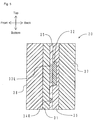
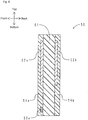
- Fig. 6 illustrates a cross-section view of the laminate film 41.
- the laminate film 41 has an outer resin layer 410, a metal foil 411 and an inner resin layer 412.
- the outer resin layer 410 is made from polyethylene naphthalate (PEN) and forms the outermost layer of the exterior packaging bag 40.
- the outer resin layer 410 has a thickness of about 12 ⁇ m.
- the inner resin layer 412 is made from polypropylene (PP) and forms the innermost layer of the exterior packaging bag 40.
- the inner resin layer 412 has a thickness of about 40 ⁇ m.
- the metal foil 411 is made from aluminum (Al) and is interposed between the outer resin layer 410 and the inner resin layer 412.
- the metal foil 411 has a thickness of about 7 ⁇ m.
- the exterior packaging bag 40 having one opening side is prepared by superimposing the two sheets of laminate films 41 and 42 and heat fusion bonding three surrounding edges.
- the body unit 300 of the sensor element 30 is housed in the exterior packaging bag 40.
- the wiring unit 301 projects out from the exterior packaging bag 40.
- the exterior packaging bag 40 is deaerated, and the opening of the exterior packaging bag 40 is sandwiched using the packing member 20 and sealed.
- the sensor assembly 3 is prepared.
- the prepared sensor assembly 3 together with the packing member 20 are installed to the assembly mounting opening 220 of the case body 22 of the circuit case 2.
- the wiring unit 301 is inserted into the inside of the case body 22.
- the wiring unit 301 is connected to the connector 21.
- the surrounding of the wiring unit 301 is secured using a sealant material.
- the load is divided by the convex portions 380 of the load transmitting plate 38, and is transmitted to the sensor element 30. That is, the constraining plate 31 and the sensor thin film 32 are depressed by the convex portions 380 of a certain curvature.
- the film thickness of the sensor thin film 32 is small. For this reason, the sensor thin film 32 almost does not compressively deform. Further, deformation of the front surface of the sensor thin film 32 is restricted by the constraining plate 31.
- the elastic plate 37 compressively deforms in such a manner as to compress in the front-rear direction. Along with this, the sensor thin film 32 bends in such a manner as to deflect backward.
- Data such as the electrical resistance, voltage, and the like of the sensor thin film 32 are sent via the wirings 34R and 34L, the connector 21, the circuit substrate 24 and the external connection connector 23 to the external occupant protection ECU, and are processed.
- the sensor module 1 detects an input load based on an increase in the electrical resistance of the sensor thin film 32.
- the wiring unit 301 of the sensor element 30 is housed inside the case body 22 of the circuit case 2. For this reason, the wiring unit 301 is unlikely to be damaged by an impact and the like. Further, the circuit case 2 is sealed. For this reason, deterioration of the wiring unit 301 is inhibited. Further, the opening of the exterior packaging bag 40 on the left edge is sealed by the packing member 20 inside the case body 22. This inhibits penetration of oxygen and moisture into the exterior packaging bag 40 via the opening. Thus, deterioration of the body unit 300 of the sensor element 30 is inhibited. Therefore, the sensor module 1 according to the present embodiment is superior in durability and ensures a long life.
- the outer resin layer 410 of the exterior packaging bag 40 is made from polyethylene naphthalate (PEN), and the inner resin layer 412 of the exterior packaging bag 40 is made from polypropylene (PP).
- PEN polyethylene naphthalate
- PP polypropylene
- PEN has superior heat and humidity resistance, heat resistance, and chemical resistance. Therefore, the exterior packaging bag 40 has high heat and humidity resistance, heat resistance, and chemical resistance.
- PP has a melting point lower than that of PEN. Therefore, by heat fusion bonding, the laminate films 41 and 42 can be easily bonded.
- the metal foil 411 of the exterior packaging bag 40 is made of aluminum (Al). Al has a superior moisture-proof property and is also highly conductive. For this reason, a socalled Faraday cage can be formed surrounding the body unit 300. Therefore, an electromagnetic wave generated by the body unit 300 can be inhibited from leaking to the outside of the exterior packaging bag 40. Therefore, noise in the electrical circuit can be reduced. By grounding the metal foil 411, the electromagnetic wave can
- a load is divided by the convex portions 380 of the load transmitting plate 38 to be input to the sensor thin film 32.
- the convex portions 380 are formed in a curved surface shape of a predetermined curvature. For this reason, when a load is input to the sensor thin film 32, the shape of the colliding object is hardly reflected. Further, a bending deformation of the sensor thin film 32 is induced by the constraining plate 31 and the elastic plate 37. That is, the energy of the input load is used on bending the sensor thin film 32. Therefore, according to the sensor assembly 3, by measuring the change in the electrical resistance based on the bending deformation of the sensor thin film 32, the load can be accurately detected regardless of the size and shape of the colliding object.
- the insulation plate 60a is made of silicone rubber and has a belt-like shape extending in the left-right direction.
- the insulation plate 60a has a width (length in the up-down direction) of about the same as that of the body unit 500 of the sensor element 50. Further, the insulation plate 60a has a length (length in the left-right direction) of about the same as that of the body unit 500 of the sensor element 50.
- the insulation plate 60a is arranged on the front side of the body unit 500 of the sensor element 50.
- the insulation plate 60b is made of silicone rubber and has a belt-like shape extending in the left-right direction.
- the insulation plate 60b has a width (length in the up-down direction) of about the same as that of the body unit 500 of the sensor element 50. Further, the insulation plate 60b has a length (length in the left-right direction) of about the same as that of the body unit 500 of the sensor element 50.
- the insulation plate 60b is arranged on the rear side of the body unit 500 of the sensor element 50.
- the wiring 53a connects to each of the electrodes 52a formed on the front surface of the sensor thin film 51.
- the wiring 53a is formed on the front surface of the sensor thin film 51 by using screen printing.
- the wiring 53b connects to each of the electrodes 52b (illustrated by dotted lines in Fig. 8 ) formed on the rear surface of the sensor thin film 51.
- the wiring 53b is formed on the rear surface of the sensor thin film 51 by using screen printing.
- the wirings 53a and 53b are formed from an elastomeric material in which silver powder is filled in urethane rubber.
- the cover film 54a is made of acrylic rubber, and has a belt-like shape extending in the left-right direction.
- the cover film 54a covers the front surface of the sensor thin film 51, the electrodes 52a, and the wiring 53a.
- the cover film 54b is made of acrylic rubber, and has a belt-like shape extending in the left-right direction.
- the cover film 54b covers the rear surface of the sensor thin film 51, the electrodes 52b, and the wiring 53b.
- the film member 61b has a width (length in the up-down direction) of about the same as that of the body unit 300 of the sensor element 30. Further, the film member 61b has a length (length in the left-right direction) of about the same as that of the body unit 300 of the sensor element 30. The film member 61b is arranged on the rear side of the body unit 300 of the sensor element 30.
- the sensor module according to the present embodiment is installed on the back side (rear side) of the front bumper so that a load is input to the sensor assembly via the front bumper. Therefore, in the present embodiment, directions in the above-mentioned Fig. 1 are defined so that the front and rear sides are reversed.
- a load is input from front to the front bumper. Thereafter, along with the deformation of the front bumper, the load is transmitted to the sensor assembly. That is, the load is input to the sensor element from the side of a base material, which will be described later.
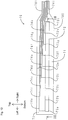
- Fig. 12 illustrates a rear view of the sensor element in the sensor assembly according to the present embodiment.
- Fig. 13 illustrates a cross-section view along a line XIII-XIII in Fig. 12 .
- Fig. 14 illustrates an enlarged view within a circle XIV in Fig. 13 .
- the cover film is illustrated with the right half removed.
- the sensor element 70 has a body unit 700 and a wiring unit 701.
- the body unit 700 has a sensor thin film 72, which will be described later.
- the body unit 700 detects deformation of the front bumper (measured object).
- the body unit 700 is enclosed in the exterior packaging bag 40 (see above-mentioned Fig. 1 ).
- the wiring unit 701 has wirings 74a-74i, which will be described later.
- the wiring unit 701 projects out from the exterior packaging bag 40 toward the right side.
- the sensor thin film 72 has a belt-like shape extending in the left-right direction.
- the sensor thin film 72 has a film thickness of about 100 ⁇ m.
- the sensor thin film 72 is secured on the rear surface of the base material 71.
- the sensor thin film 72 is formed in which carbon beads (conductive filler) are filled in epoxy resin.
- the filling rate of the carbon beads is about 45% by volume when the volume of the sensor thin film 72 is 100% by volume.
- Fig. 14 schematically illustrates, in the sensor thin film 72, a plurality of cracks C1 are formed in advance.
- the cracks C1 are arranged extending in a direction intersecting the arrangement direction (left-right direction) of the electrodes 73a - 73i, that is, in the thickness direction (front-rear direction) of the sensor thin film 72. About two of the cracks C1 are formed in each unit section U1 of about 2 mm along the left-right direction of the sensor thin film 72.
- the production method of the sensor element 70 includes a coating material preparation process, a printing process, a bending curing process, an unloading process, and a cover film forming process.
- coating materials for forming the sensor thin film 72, the electrodes 73a - 73i, the wirings 74a - 74i, and the cover film 75 are respectively prepared.
- coating materials, except a cover film coating material are printed on the surface of the base material using screen printing equipment.
- an electrode coating material and a wiring coating material are sequentially printed.
- the coated film is cured, and the electrodes 73a - 73i and the wirings 74a - 74i are formed.
- a sensor coating material is printed on the surface of the base material 71 on which the electrodes 73a - 73i are formed.
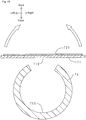
- Fig. 15 illustrates a schematic view of a first half of the bending curing process.
- Fig. 16 illustrates a schematic view of a second half of the bending curing process.
- the base material 71 on which the coated film 720 of the sensor coating material is formed is applied to an inner periphery 760 of a C-shaped mold 76.
- a front surface 710 of the base material 71 is in contact with the inner periphery 760 of the mold 76.
- the mold 76 is placed in a drying furnace and kept for 1 hour at a temperature of about 140 °C to subject the coated film 720 to a primary curing.
- the coated film 720 is kept for 2 hours at a temperature of about 170 °C to subject the coated film 720 to a secondary curing.
- the base material 71 together with the cured coated film 720 are peeled off from the mold 76, and the base material 71 and the cured coated film 720 are restored from the bent state to their original planar state (see above-mentioned Fig. 15 ).
- a strain is input to the cured coated film 720 (sensor thin film 72) and cracks are formed therein. As described above, the sensor thin film 72 is formed.
- the sensor assembly and the sensor module according to the present embodiment have the same operation effects as the sensor assembly and the sensor module according to the first embodiment with respect to the portions having common configurations.
- the bending of the sensor thin film 72 causes the cracks C1 to open up. This causes the conductive paths to be cut off and the electrical resistance of the sensor thin film 72 to rapidly increase. Therefore, response delay is small.
- the conductive paths are cut off primarily due to opening up of the cracks C1. Therefore, as compared to the case where the cutting off of the conductive paths depends only on the elastic deformation of the parent material (see above-mentioned Fig. 17 ), even a small strain can be detected with a good accuracy.
- the response speed is less dependent on atmospheric temperature and the input speed of a strain.
- the sensor thin film 72 is covered by the cover film 75. This inhibits deterioration of the sensor thin film 72. Further, when the load is removed after the bending deformation, with the help of the elastic restoring force of the cover film 75, the sensor thin film 72 easily restores its original shape.
- the exterior packaging bag is formed from a laminate film having a PEN/Al/PP three-layer structure.
- the configuration of the laminate film is not limited to the above embodiments.
- the resin of the outer resin layer polyphenylene sulfide (PPS), polyethylene terephthalate (PET), polyethylene (PE), polypropylene (PP), polyamide (PA), polycarbonate (PC), polyoxymethylene (POM), polymethylmethacrylate (PMMA), polyvinyl chloride resin (PVC), fluorine resin (polytetrafluoroethylene (PTFE), tetrafluoroethylene-ethylene copolymer (ETFE), and the like), ethylene-vinyl alcohol copolymer resin (EVOH), and the like, may be used.
- PPS polyphenylene sulfide
- PET polyethylene terephthalate
- PE polyethylene
- PP polypropylene
- PA polyamide
- PC polycarbonate
- POM polyoxymethylene
- PMMA polymethylme
- the metal foil tin, copper, stainless steel, zinc, and the like
- the resin of the inner resin layer similar to the outer resin layer, PPS, PET, PE, PP, PA, PC, POM, PMMA, PVC, fluorine resin (PTFE, ETFE, and the like), EVOH, and the like, may be used. It is desirable that a resin used for the inner resin layer have a melting point lower than that of the outer resin layer. Further, as needed, other layers may be laminated on the above three layers to form a structure of four or more layers. Further, thickness of each layer is not particularly limited.
- a sensor element is used in which electrical resistance of the sensor thin film changes due to a deformation.
- a sensor element is used in which capacitance changes due to a deformation.
- the type, configuration, shape, size, and the like of the sensor element are not limited to the above embodiments.
- the parent material of the sensor thin film may be suitably selected from resin and elastomer, by taking into account compatibility with the conductive filler.
- the number of the electrodes and arrangement locations may be suitably set.
- the base material (including the constraining plate and the insulation films) and the material of the cover film are not particularly limited as long as they are insulating materials. It is desirable that the base material be a material that can restrict a deformation of one side of the sensor thin film.
- flexible resin films such as PE, PEN and the like are preferred.
- the insulation film and cover film are not arranged.
- the material, shape, and the like of the elastic plate and the load transmitting plate are not particularly limited.
- the convex portions all have the same curvature.
- the curvature of the convex portions By varying the curvature of the convex portions, the relation between a load and an output can be adjusted.
- the greater the curvature of the convex portions of the load transmitting plate is, the greater the amount of bending deformation of the sensor thin film due to depressing by the convex portions will be. Therefore, detection sensitivity of a load can be improved.
- the number of the convex portions may be suitably determined by taking into account the shape and size of an anticipated colliding object. The greater the number of convex portions is, the more finely the shape of the colliding object can be divided. For this reason, dependence on the shape of the colliding object can be further reduced. It is also possible that the elastic plate and the load transmitting plate are not arranged.
- the method for forming the cracks in the sensor thin film is not particularly limited.
- the sensor thin film be further subjected to bending processing. By doing so, cracks can be increased in number and can be dispersed in the parent material. Further, by devising distribution and the like of the convexo-concave portions to be formed, distribution of the cracks and the like can be adjusted.
- the type of the elastomer of the sensor thin film is not particularly limited.
- a material having a large relative permittivity is preferred.
- the electrodes and wirings be flexible and deformable together with the sensor thin film.
- three pairs of opposing electrodes are formed across the sensor thin film.
- the number, size, arrangement, and the like of the electrodes may be suitably determined according to an intended use.
- the electrodes and wirings are formed on the front surface and rear surface of the sensor thin film, respectively.
- the sensor thin film, the electrodes, and the wirings may also be formed on a surface of an insulating base material. It is also possible that the cover film is not arranged.
- the material of the insulation plate is not particularly limited as long as it is an insulating material. Various elastomers, including silicone rubber, can be used.
- the material of the film member is not particularly limited. From a point of view of having a small friction coefficient, in addition to POM, fluorine resin such as PTFE and ETFE are preferable.
- one edge of the exterior packaging bag is sealed by using the packing member.
- the shape, material, and the like of the packing member are not particularly limited.
- the shape and material of the circuit case, as well as the manner in which the circuit case connects to an external electronic device, and the like, are not particularly limited.
- Heat and humidity resistance of the exterior packaging bag used in the above embodiments was experimentally evaluated.
- three kinds of exterior packaging bags having different kinds of outer resin layers were prepared.
- One of the outer resin layers of the three kinds of exterior packaging bags was made of polyethylene naphthalate (PEN), which was the same as in the above embodiments.
- the remaining two were respectively made of polyphenylene sulfide (PPS) and polyethylene terephthalate (PET).
- the outer resin layers all had a thickness of 12 ⁇ m. Configurations other than the outer resin layers of the exterior packaging bags were the same as in the above embodiments.
- a temperature and humidity sensor was placed in each of the exterior packaging bags, and after deaeration, the opening was sealed using the packing member.
- Fig. 11 illustrates measurement results of the humidity inside the exterior packaging bags.
- Fig. 11 illustrates, in all of the exterior packaging bags, the internal humidity was maintained at 5% or less.
- the internal temperature was constant at about 85 °C.
- the exterior packaging bag formed from the laminate film having a structure of resin layer / metal foil / resin layer has superior heat and humidity resistance. Therefore, by enclosing a component such as a sensor element and the like in the exterior packaging bag, deterioration of the sensor component in a hot and humid environment can be inhibited. That is, the sensor assembly and the sensor module according to the present invention have superior heat and humidity resistance and ensure a long life.
- the sensor assembly and the sensor module according to the present invention can be applied to various applications including a collision sensor in an automobile and the like; a soft pressure sensor such as a seating sensor and artificial skin; a data input device such as a keyboard; a surface pressure distribution sensor for a bed and a carpet; and the like.
Description
- The present invention relates to a sensor assembly having a flexible sensor element that uses a polymer material. More specifically, the present invention relates to a sensor assembly having a sensor component such as a sensor element or the like that is less likely to deteriorate and is superior in durability.
- As a means for detecting a vehicle collision and the like, there is a load sensor using optical fiber (for example, see Patent Document 1). In a load sensor of this type, when the optical fiber deforms due to a collision, loss of light transmitting from one end to the other end of the optical fiber becomes greater. Based on this loss of light, whether there is a collision is judged. The optical fiber is attached to a resin retaining plate.
- On the other hand, the present applicant has proposed a load sensor having an elastomeric sensor thin film (for example, see
Patent Documents 2 and 3). In a load sensor disclosed inPatent Document 2, a sensor thin film is formed in which conductive filler is filled in elastomer of a parent material at a predetermined state. According to this load sensor, based on a change in electrical resistance caused when the sensor thin film elastically deforms, an input load can be detected. A load sensor disclosed inPatent Document 3 is a capacitance-type sensor, which includes an elastomeric dielectric film and a pair of electrodes arranged sandwiching the dielectric film. According to this load sensor, based on a change in capacitance between the pair of electrodes, an input load can be detected. -
- Patent Document 1: Japanese Patent Laid-Open Publication No.
2007-153073 - Patent Document 2: Japanese Patent Laid-Open Publication No.
2008-107199 - Patent Document 3: Japanese Patent Laid-Open Publication No.
2009-20006 - Patent Document 4: Japanese Patent Laid-Open Publication No.
2008-175659 -
JP 2002 350250 A -
JP 5 281664 A - A load sensor is required to have durability according to a usage environment. For example, when used in a vehicle, a load sensor is required to have heat and humidity resistance, chemical resistance, weather resistance, and the like. In this regard, components of the load sensors of the
above Patent Documents - The present invention is devised in view of such circumstances. A purpose of the present invention is to provide a sensor assembly and a sensor module having a flexible sensor element that uses polymer material and having a component such as the sensor element or the like that is less likely to deteriorate and is superior in durability.
- According to the invention a sensor assembly is defined in
Claim 1 and a sensor module is defined inClaim 6. - (1) A sensor assembly according to the present invention includes a sensor element; and an exterior packaging bag enclosing the sensor element. The sensor element includes a sensor thin film made of resin or elastomer; and at least one pair of electrodes connected to the sensor thin film. The exterior packaging bag is formed from a laminate film having a metal foil and two resin layers arranged sandwiching the metal foil.
In the sensor assembly of the present invention, the sensor element is enclosed inside the exterior packaging bag. The exterior packaging bag is formed from the laminate film having a metal foil and two resin layers. The laminate film is hard for oxygen and moisture to pass through. Therefore, contact between the sensor element, and oxygen and moisture is inhibited. For this reason, the sensor element hardly deteriorates. That is, for example, even when the sensor assembly of the present invention is arranged in a hot and humid environment, the sensor thin film and the like are less likely to hydrolyze. Further, silver in the wiring is also less likely to cause migration. Therefore, the sensor assembly of the present invention is superior in durability and ensures a long life. Further, contact between the sensor element, and oxygen and moisture is inhibited. Therefore, the level of humidity resistance or the like that is required for a sensor material can be lowered. This allows material cost to be reduced. In the present specification, "elastomer" includes rubber and thermoplastic elastomer.
The laminate film is thin and flexible and has a high degree of freedom with respect to its shape. Therefore, by forming the exterior packaging bag from the laminate film, regardless of the size and the shape such as a sheet-like shape and a belt-like shape of the sensor element, the sensor element can be housed in the exterior packaging bag. Further, the sensor assembly can be made thinner and more light weighted. Further, the sensor element can be covered along the shape of the outer edge of the sensor element. For this reason, a void is unlikely to occur between the exterior packaging bag and the sensor element.
In the laminate film, the metal foil is interposed between the two resin layers. The metal foil is conductive. Therefore, by grounding the metal foil, electromagnetic waves generated by the sensor element can be allowed to escape. This allows noise in an electrical circuit to be reduced. Further, by suitably selecting the type of the resin layer according to a usage environment, features such as chemical resistance, heat resistance, weather resistance, strength and the like can be imparted to the laminate film.
The sensor thin film is made from elastomer; the pair of electrodes be arranged across the sensor thin film; and the sensor element be capable of detecting an input load based on a change in capacitance between the pair of electrodes.
Generally, the capacitance of a capacitance-type sensor formed by interposing a dielectric film between a pair of electrodes can be obtained according to the following equation (I).
C = ε0εrS/d (I)
[where C is the capacitance; ε0 is the vacuum permittivity; εr is the relative permittivity of the dielectric film; S is the electrode area; and d is the distance between the electrodes] In the present configuration, when the sensor element is depressed, the sensor thin film (dielectric film) is compressed and stretched in a direction parallel to the surfaces of the electrodes. According to the above equation (I), when the thickness of the sensor thin film, that is, the distance d between the electrodes, decreases, the capacitance C between the electrodes increases. According to the present configuration, based on this change in the capacitance, the input load can be detected. - (2) It is desirable that, in the configuration of the above aspect (1), of the two resin layers, an inner resin layer arranged on an inner side have a melting point lower than that of an outer resin layer arranged on an outer side.
Sealing of the exterior packaging bag is performed by fusion bonding an overlapping portion of the laminate film using heat or ultrasound. The inner adhesion layer is melt by heat or ultrasound, and plays a role of bonding the overlapping portion. For this reason, it is desirable that the inner adhesion layer be configured with resin of a relatively low melting point. According to the present configuration, the inner adhesion layer is easy to be fusion-bonded. Therefore, the laminate film can be easily sealed.
Depending on the type of the outer resin layer, as the resin of the inner resin layer, for example, at least one kind selected from polyphenylene sulfide, polyethylene terephthalate, polyethylene naphthalate, polyethylene, polypropylene, acid-modified polyolefin, polyamide, polycarbonate, polyoxymethylene, polymethylmethacrylate, polyvinyl chloride resin, fluorine resin, and ethylene-vinyl alcohol copolymer resin can be used. For the reason of having a lower melting point, polypropylene, polyethylene, and acid-modified polyolefin are preferable.
Further, it is desirable that the inner resin layer have a thickness of 5 µm or more and 200 µm or less. When the thickness is less than 5 µm, peeling strength (sealing property) may deteriorate. It is preferred that the thickness be 20 µm or more. On the other hand, when the thickness is above 200 µm, the film thickness of the laminate film increases. Therefore, sensor sensitivity may deteriorate. It is preferred that the thickness be 100 µm or less. - (3) It is desirable that, in the configuration of the above aspect (2), the outer resin layer be made from at least one kind selected from polyphenylene sulfide, polyethylene terephthalate, polyethylene naphthalate, polyethylene, polypropylene, polyamide, polycarbonate, polyoxymethylene, polymethylmethacrylate, polyvinyl chloride resin, fluorine resin, and ethylene-vinyl alcohol copolymer resin.
As the resin of the outer resin layer, a resin, having features such as heat and humidity resistance, heat resistance, chemical resistance, weather resistance, strength, and the like, can be suitably selected according to a usage environment. According to the present configuration, a laminate film (exterior packaging bag) superior particularly in heat and humidity resistance, heat resistance, and chemical resistance can be obtained. Of the above-mentioned materials, for the reason of having high heat resistance and heat and humidity resistance, polyphenylene sulfide, polyethylene terephthalate and polyethylene naphthalate are preferable.
Further, it is desirable that the outer resin layer have a thickness of 5 µm or more and 100 µm or less. When the thickness is less than 5 µm, strength of the laminate film may deteriorate. It is preferred that the thickness be 10 µm or more. On the other hand, when the thickness is above 100 µm, the film thickness of the laminate film increases. Therefore, sensor sensitivity may deteriorate. It is preferred that the thickness be 50 µm or less. - (4) It is desirable that, in the configuration of the above aspect (1), the metal foil be made from at least one kind selected from aluminum, tin, copper, stainless steel, and zinc.
The metal foil plays a role of inhibiting penetration of oxygen, moisture, and the like. Further, the metal foil is conductive, and therefore, as described above, can be used for noise reduction. From the point view of conductivity, it is desirable that the metal foil have a volume resistivity of 10-3 Ω·cm or less. According to the present configuration, the effect of inhibiting penetration of oxygen, moisture, and the like can be improved. Of the above-mentioned metals, aluminum is light in weight, has good stretchability, and is less expensive, and thus is preferred.
Further, it is desirable that the metal foil have a thickness of 0.1 µm or more and 80 µm or less. When the thickness is less than 0.1 µm, the effect to inhibit water penetration may deteriorate. It is preferred that the thickness be 1 µm or more. On the other hand, when the thickness is above 80 µm, the film thickness of the laminate film increases. Therefore, sensor sensitivity may deteriorate. It is preferred that the thickness be 50 µm or less. - (5) It is desirable that, in the configuration of the above aspect (1), a film member be interposed between the exterior packaging bag and the sensor element, the film member having a friction coefficient smaller than that of at least one of an inner surface of the exterior packaging bag and an outermost surface of the sensor element.
For example, when the sensor assembly of the present invention is depressed, the sensor element deforms. The load applied during the depression is detected based on the deformation of the sensor element. In this case, when the exterior packaging bag and the sensor element are firmly attached to each other, the deformation of the sensor element is inhibited by the exterior packaging bag. For this reason, the load cannot be accurately detected. Therefore, it is desirable that the exterior packaging bag do not inhibit the deformation of the sensor element. That is, it is desirable that the friction between the exterior packaging bag and the sensor element be as small as possible. According to the present configuration, the film member, having a friction coefficient smaller than that of at least one of the inner surface of the exterior packaging bag and the outermost surface of the sensor element, is interposed between the exterior packaging bag and the sensor element. Here, the outermost surface of the sensor element is the surface in contact with the exterior packaging bag in the case where the film member is absent. Therefore, the sensor element becomes slick inside the exterior packaging bag, and thus can easily deform. This allows a load to be accurately detected. In the present configuration, the friction coefficients may be compared using static friction coefficients.
As the film member, for example, polyoxymethylene, and fluorine resin such as polytetrafluoroethylene and tetrafluoroethylene-ethylene copolymer, are preferred. - (6) It is desirable that, in the configuration of the above aspect (1), the sensor thin film be formed in which a conductive filler is filled in a resin or elastomeric parent material; and the sensor element further include an insulating base material arranged on a surface of the sensor thin film, and is capable of detecting an input load based on a change in electrical resistance due to deformation of the sensor thin film.
With respect to the deformation of the sensor thin film, the electrical resistance may increase or decrease. The change behavior of the electrical resistance with respect to the deformation of the sensor thin film can be adjusted by adjusting the type of the elastomer of the parent material, the type of the conductive filler, the amount of the conductive filler, and the like.
For example, it is preferable that spherical conductive filler is filled in the parent material in a nearly single-particle state and at a high filling rate. Here, the "nearly single-particle state" means that, when the total weight of the conductive filler is 100% by weight, 50% or more by weight of the particles of the conductive filler exist in an independent primary particle state rather than as agglomerated secondary particles. The "high filling rate" means that the conductive filler is filled in a nearly close-packed state. By doing so, in a state in which a load is not input (which may be referred to as a "no-load" state" in the following), three-dimensional conductive paths can be formed in the parent material via contact among the particles of the conductive filler. Therefore, in the no-load state, the sensor thin film is highly conductive. For example, when the sensor thin film deforms, the contact state among the particles of the conductive filler changes. This causes the three-dimensional conductive paths to collapse and the electrical resistance to increase. As the deformation amount increases, the electrical resistance increases. - (7) It is desirable that, in the configuration of the above aspect (6), the sensor element further include an elastic plate, which is arranged on the sensor thin film side or the base material side, and which elastically deforms due to an input load, thereby causing the sensor thin film to undergo a bending deformation; and the sensor element be capable of detecting the input load based on a change in electrical resistance due to the bending deformation of the sensor thin film.
In the sensor thin film, various stresses such as compression and tension are applied depending on the input form of the load. However, the change behavior of the electrical resistance of the sensor thin film is different depending on the type of the stress. For example, in the case where the electrical resistance increases with respect to the deformation of the sensor thin film, the increase behavior of the electrical resistance with respect to compression and the increase behavior of the electrical resistance with respect to tension are different. Therefore, in the case where a compressive stress and a tensile stress are mixed, the electrical resistance is unlikely to linearly change with respect to the size of the load. For this reason, it is difficult to accurately detect the load.
In this regard, according to the present configuration, the elastic plate is arranged on the sensor thin film side or the base material side. When a load is applied, the elastic plate is compressed and elastically deforms in a manner deflecting toward the load input direction. Along with the deformation of the elastic plate, the sensor thin film undergoes bending deformation. That is, the energy of the input load is used on bending the sensor thin film. Therefore, according to the present configuration, change in the electrical resistance with respect to the bending deformation of the sensor thin film is output. This allows the load to be accurately detected regardless of the input form of the load.
Further, the spring constant of the elastic plate varies depending on the material, shape (area, thickness), and the like. Therefore, elastic deformation amount (deflection amount) with respect to a load can be adjusted by the material, shape, and the like of the elastic plate. This allows the value of the electrical resistance with respect to the bending deformation amount of the sensor thin film to be set within a desired range. Further, due to a restoring force of the elastic plate, reproducibility of a response with respect to the load is high. Further, impact of the input load is absorbed by the elastic plate. For this reason, damage to the sensor element is reduced. - (8) It is desirable that, in the configuration of the above aspect (6) or aspect (7), the sensor element further include a load transmitting plate arranged more on a load input side than the sensor thin film; the load transmitting plate have a plurality of convex portions having curved surface shapes; and the input load be transmitted to the sensor thin film via the plurality of convex portions.
According to the present configuration, an input load is transmitted to the sensor thin film via the load transmitting plate. That is, the input load is divided by the plurality of convex portions to be transmitted to the sensor thin film. The convex portions are formed in a curved surface shape of a predetermined curvature. For this reason, regardless of the shape of a colliding object that inputs the load, the load is input to the sensor thin film at a predetermined curvature. That is, when a load is input to the sensor thin film, the shape of the colliding object is hardly reflected. Therefore, according to the present configuration, the load can be accurately detected without depending on the shape of the colliding object. - (9) It is desirable that, in the configuration of the above aspect (1), the sensor thin film be formed in which a conductive filler is filled at a filing rate of 30% or more by volume in a resin parent material; three-dimensional conductive paths be formed in the sensor thin film via contact among the particles of the conductive filler; and the sensor element further include an insulating base material arranged on a surface of the sensor thin film, and be capable of detecting deformation of a measured object based on an increase in electrical resistance with respect to bending deformation of the sensor thin film.
In the present configuration, the sensor thin film is formed in which conductive filler is filled at a high filling rate in a resin parent material. The filling rate of the conductive filler is a value when the volume of the sensor thin film is 100% by volume. The filling rate of the conductive filler is high. Therefore, in the sensor thin film in the no-load state, three-dimensional conductive paths are formed via contact among the particles of the conductive filler. Therefore, in the no-load state, the sensor thin film is highly conductive.
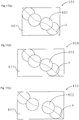
Figs. 17(a) - 17(c) illustrate enlarged schematic views near a portion of the conductive filler in the sensor thin film. Here,Figs. 17(a) - 17(c) are schematic views for explaining the sensor thin film. Therefore,Figs. 17(a) - 17(c) , including the shape of the particles of the conductive filler, the shape of the conductive paths, the extension direction of the conductive paths, and the like, are not to be considered as limiting in any way the configuration of the sensor thin film.Figs. 17(a) - 17(c) respectively illustrate a no-load state before a bending deformation, a state immediately after the bending deformation, and a state further after the state immediately after the bending deformation. AsFig. 17(a) illustrates, the sensorthin film 800 hasmatrix resin 801 andconductive filler particles 802. In the sensorthin film 800, a conductive path P is formed by contact amongconductive filler particles 802. When a load is applied to the sensorthin film 800, the sensorthin film 800 starts a bending deformation. AsFig. 17(b) illustrates, along with the start of the bending deformation, thematrix resin 801 is stretched in the left-right direction in the drawing. This causes theconductive filler particles 802 to repel each other and the contact state of theconductive filler particles 802 to change. AsFig. 17(c) illustrates, as the sensorthin film 800 bends further, thematrix resin 801 is stretched further. This causes the contact among theconductive filler particles 802 to be broken and the conductive path P to be cut off. As a result, the electrical resistance increases. When the applied load is removed, the sensorthin film 800 restores its original state (the state illustrated inFig. 17(a) ) by an elastic restoring force of thematrix resin 801.
As described above, in the sensor thin film of the present configuration, the electrical resistance increases as the bending deformation amount increases. This allows the sensor element of the present configuration to detect deformation of a measured object. Further, the sensor thin film is arranged on the surface of the base material. By adjusting the thickness of the base material, sensitivity of the sensor element can be adjusted. For example, in a case where the center of curvature during a bending deformation is on the rear side of the base material, when the thickness of the base material is increased, a strain amount of the sensor thin film during the bending deformation increases. That is, when a total thickness of the base material and the sensor thin film is denoted by t, and a radius of curvature extending from the center of curvature to the rear surface of the base material during a bending deformation is denoted by R, the strain amount ε is given by ε = t/R. For this reason, when the thickness of the base material is increased, the strain amount of the sensor thin film during a bending deformation increases. This improves the sensitivity of the sensor element. - (10) It is desirable that, in the configuration of the above aspect (9), the sensor element further include an elastically deformable cover film arranged in a manner covering the sensor thin film; and cracks be formed in advance in the sensor thin film in such a direction that the conductive paths are cut off when a bending deformation occurs.
In the configuration of the above aspect (9), when the sensor thin film undergoes a bending deformation, the elastic deformation of the parent material causes the conductive paths to collapse and the electrical resistance of the sensor thin film to increase. That is, the sensor element uses the increase in the electrical resistance in the elastic region of the parent material of the sensor thin film to detect the deformation of a measured object. However, it takes time from an input of a strain until the parent material elastically deforms. For this reason, in detecting a deformation in the elastic region of the parent material, the response is delayed by the time required for the elastic deformation of the parent material. Therefore, detection accuracy decreases. In particular, for a fast bending deformation, the response delay further increases and thus the detection accuracy is likely to further decrease. Further, the speed of the elastic deformation of the parent material is influenced by the input speed of a strain and the atmospheric temperature. For this reason, the input speed of the strain and the atmospheric temperature also contribute to the decrease in the detection accuracy.
According to the present configuration, cracks are formed in advance in the sensor thin film. The cracks are formed in such a direction that the conductive paths are cut off when a bending deformation occurs.Figs. 18(a) and 18(b) illustrate enlarged schematic views near a portion of a crack in the sensor thin film. Here,Figs. 18(a) and 18(b) are schematic views for explaining the sensor thin film. Therefore,Figs. 18(a) and 18(b) , including the shape of the crack, the extension direction of the crack, the shape of the particles of the conductive filler, the shape of the conductive path, the extension direction of the conductive path, and the like, are not to be considered as limiting in any way the configuration of the sensor thin film.Figs. 18(a) and 18(b) respectively illustrate a no-load state before a bending deformation and a state after the bending deformation.
AsFig. 18(a) illustrates, the sensorthin film 800 hasmatrix resin 801,conductive filler particles 802, and acrack 803. In the sensorthin film 800, a conductive path P is formed by contact amongconductive filler particles 802. Thecrack 803 is formed along a direction crossing the left-right direction (extension direction) in the figure. When a load is applied to the sensorthin film 800, the sensorthin film 800 starts a bending deformation. When the sensorthin film 800 is stretched in the left-right direction due to the bending deformation, asFig. 18(b) illustrates, thecrack 803 opens up. This causes the contact among theconductive filler particles 802 to be broken and the conductive path P to be cut off. As a result, the electrical resistance increases. When the applied load is removed, the sensorthin film 800 restores its original state (the state illustrated inFig. 18(a) ). This also causes thecrack 803 to return to its original state.
As described above, according to the sensor thin film of the present configuration, when a strain is input due to a bending deformation, the conductive paths are cut off without waiting for an elastic deformation of the matrix resin (however, the case where the conductive paths are cut off due to an elastic deformation of the matrix resin is not excluded). Therefore, a response delay is unlikely to occur.
Further, the conductive paths are cut off primarily due to the opening up of the cracks. Therefore, as compared to the case where the cutting off of the conductive paths depends only the elastic deformation of the matrix resin (see above-mentionedFigs. 17(a) - 17(c) ), even a small strain can be accurately detected.
Further, as described above, the speed of an elastic deformation of the matrix resin is influenced by the atmospheric temperature. With respect to this point, the conductive paths in the sensor thin film of the present configuration are cut off primarily due to the opening up of the cracks. For this reason, as compared to the case where the conductive paths are cut off depending only on the elastic deformation of the matrix resin (see the above-mentionedFigs. 17(a) - 17(c) ), the response speed is less dependent on the atmospheric temperature. The response speed is also less dependent on the input speed of a strain.
Further, the sensor thin film is covered by the cover film. This inhibits deterioration of the sensor thin film. Here, the cover film is elastically deformable. Therefore, when the load is removed after the bending deformation, with the help of the elastic restoring force of the cover film, the sensor thin film easily restores its original shape. The opened up cracks also easily restore their original state. - (12) A sensor module according to the present invention includes the sensor assembly according to any one of the above aspects (1) - (10); and a circuit case on which the sensor assembly is installed. The exterior packaging bag of the sensor assembly has an opening. The sensor element has a wiring unit projecting out of the exterior packaging bag from the opening. The circuit case has a box-like shape, and includes a case body on which an assembly mounting opening is provided; a packing member sealing the opening in a state in which the wiring unit projects out from the opening of the exterior packaging bag and being installed on the assembly mounting opening of the case body; and a connector being connected to the wiring unit inside the case body and being connected to an electrical circuit.
- The sensor element has the wiring unit connected to the electrical circuit. The wiring unit is led out from the opening of the exterior packaging bag and is connected to the electrical circuit. According to the present configuration, the wiring unit is housed inside the case body of the circuit case. For this reason, the wiring unit can be protected from an impact and the like. By using the packing member, the opening of the exterior packaging bag can be easily sealed and the sensor assembly can be installed on the circuit case.
-
-
Fig. 1 is a perspective view of a sensor module according to a first embodiment. -
Fig. 2 is an exploded perspective view of the sensor module. -
Fig. 3 is an exploded perspective view of a sensor assembly in the sensor module. -
Fig. 4 is an exploded perspective view of a sensor element in the sensor assembly. -
Fig. 5 is a cross-section view in a transverse direction inFig. 4 near an electrode on a left side. -
Fig. 6 is a cross-section view of a laminate film forming an exterior packaging bag. -
Fig. 7 is an exploded perspective view of a sensor assembly according to a second embodiment. -
Fig. 8 is a front view of a sensor element in the sensor assembly. -
Fig. 9 is a cross-section view along a line IX-IX inFig. 8 . -
Fig. 10 is an exploded perspective view of a sensor assembly according to a third embodiment. -
Fig. 11 is a graph illustrating measurement results of humidity inside an exterior packaging bag according to a working example. -
Fig. 12 is rear view of a sensor element in a sensor assembly according to a fourth embodiment. -
Fig. 13 is a cross-section view along a line XIII-XIII inFig. 12 . -
Fig. 14 is an enlarged view within a circle XIV inFig. 13 . -
Fig. 15 is a schematic view of a first half of a bending curing process of a production method of a sensor element according to the fourth embodiment. -
Fig. 16 is a schematic view of a second half of the bending curing process. -
Fig. 17(a) is an enlarged schematic view near a portion of conductive filler in a sensor thin film in a no-load state before a bending deformation. -
Fig. 17(b) is an enlarged schematic view near the portion of the conductive filler in the sensor thin film in a state immediately after the bending deformation. -
Fig. 17(c) is an enlarged schematic view near the portion of the conductive filler in the sensor thin film in a state further after the state immediately after the bending deformation. -
Fig. 18(a) is an enlarged schematic view near a portion of a crack in the sensor thin film in the no-load state before the bending deformation. -
Fig. 18(b) is an enlarged schematic view near the portion of the crack in the sensor thin film in the state after the bending deformation. -
- 1:
- sensor module
- 2:
- circuit case
- 20:
- packing member
- 20a:
- front side securing member
- 20b:
- rear side securing member
- 21:
- connector
- 22:
- case body
- 23:
- external connection connector
- 24:
- circuit substrate (electrical circuit)
- 200a, 201a:
- recess
- 200b, 201b:
- projection
- 220:
- assembly mounting opening
- 230:
- terminal
- 3:
- sensor assembly
- 30:
- sensor element
- 31:
- constraining plate (base material)
- 32:
- sensor thin film
- 33R, 33L:
- electrode
- 34R, 34L:
- wiring
- 35:
- insulation film (base material)
- 36:
- cover film
- 37:
- elastic plate
- 38:
- load transmitting plate
- 300:
- body unit
- 301:
- wiring unit
- 380:
- convex portion
- 40:
- exterior packaging bag
- 41, 42:
- laminate film
- 410:
- outer resin layer
- 411:
- metal foil
- 412:
- inner resin layer
- 50:
- sensor element
- 51:
- sensor thin film
- 52a, 52b:
- electrode
- 53a, 53b:
- wiring
- 54a, 54b:
- cover film
- 500:
- body unit
- 501:
- wiring unit
- 60a, 60b:
- insulation plate (film member)
- 61a, 61b:
- film member
- 70:
- sensor element
- 71:
- base material
- 72:
- sensor thin film
- 73a - 73i:
- electrode
- 74a - 74i:
- wiring
- 75:
- cover film
- 76:
- mold
- 700:
- body unit
- 701:
- wiring unit
- 701:
- front
- 720:
- coated film
- 760:
- inner periphery
- 800:
- sensor thin film
- 801:
- matrix resin
- 802:
- conductive filler particles
- 803:
- crack
- C1:
- crack
- P:
- conductive path
- U1:
- unit section
- Next, embodiments of a sensor assembly and a sensor module of the present invention are explained.
- First, a configuration of a sensor module according to the present embodiment is explained.
Fig. 1 illustrates a perspective view of the sensor module according to the present embodiment.Fig. 2 illustrates an exploded perspective view of the sensor module.Fig. 3 illustrates an exploded perspective view of a sensor assembly in the sensor module. InFigs. 1 - 3 , transparently visible portions are illustrated using thin lines. - As
Figs. 1 - 3 illustrate, asensor module 1 includes acircuit case 2 and asensor assembly 3. Thesensor module 1 is installed on a surface (front surface) of a front bumper of a vehicle (not shown in the drawings). Therefore, directions in the drawings are defined relative to a traveling direction of the vehicle. In the present embodiment, a load is input to thesensor assembly 3 from the front. - The
circuit case 2 includes acase body 22, a packingmember 20, aconnector 21, anexternal connection connector 23, and acircuit substrate 24. Thecase body 22 is made of resin, and has a box-like shape. AsFig. 2 illustrates, on the front surface of thecase body 22, anassembly mounting opening 220 is provided opening toward the right. Theassembly mounting opening 220 is in communication with inside and outside of thecase body 22. - The packing
member 20 is made of resin. The packingmember 20 has a frontside securing member 20a and a rearside securing member 20b. The frontside securing member 20a has a rectangular plate-like shape. On two ends in the up-down direction on the rear surface of the frontside securing member 20a, a pair ofrecesses 200a and 201a are formed. Similarly, the rearside securing member 20b has a rectangular plate-like shape. On two ends in the up-down direction on the front surface of the rearside securing member 20b, a pair ofprojections side securing member 20a and the rearside securing member 20b are bonded by respectively fitting theprojections recesses 200a and 201 a. Between the frontside securing member 20a and the rearside securing member 20b, a left end portion (portion illustrated by hatching inFig. 3 ) of thesensor assembly 3 is sandwiched. In the state in which the left end portion of thesensor assembly 3 is sandwiched, the packingmember 20 is pressed into theassembly mounting opening 220 to be fixed. Awiring unit 301 of thesensor assembly 3 is housed inside thecase body 22 via theassembly mounting opening 220. - The
circuit substrate 24 is housed inside thecase body 22. Thecircuit substrate 24 is arranged in contact with a back wall of thecase body 22. Theconnector 21 connects to thecircuit substrate 24. Further, theconnector 21 connects to thewiring unit 301 of thesensor assembly 3 inside thecase body 22. Theexternal connection connector 23 is penetratingly provided on a left wall of thecase body 22. Theexternal connection connector 23 has a terminal 230. Theexternal connection connector 23 connects to thecircuit substrate 24 inside thecase body 22. Further, theexternal connection connector 23 connects to an occupant protection ECU (electronic control unit, not shown in the drawings) arranged outside thecase body 22. That is, thewiring unit 301 of thesensor assembly 3 connects to the occupant protection ECU on the outside via theconnector 21, thecircuit substrate 24, and theexternal connection connector 23. In the following, thesensor assembly 3 is explained in detail. - As the above-mentioned
Fig 3 illustrates, thesensor assembly 3 includes asensor element 30 and anexterior packaging bag 40. Thesensor element 30 has abody unit 300 and thewiring unit 301. Thebody unit 300 has a sensorthin film 32, which will be described later. Thebody unit 300 detects a load. Thebody unit 300 is enclosed inside theexterior packaging bag 40. Thewiring unit 301 has wirings 34R and 34L, which will be described later. Thewiring unit 301 projects out from theexterior packaging bag 40 toward the left side. -
Fig. 4 illustrates an exploded perspective view of the sensor element.Fig. 5 illustrates a cross-section view in a transverse direction inFig. 4 near an electrode on the left side. InFig. 4 , for the convenience of explanation, a constraining plate and an insulation film are transparently illustrated. InFig. 4 , transparently visible portions are illustrated using thin lines. AsFigs. 4 and5 illustrate, thebody unit 300 of thesensor element 30 includes a constrainingplate 31, the sensorthin film 32,electrodes wirings 34R and 34L, aninsulation film 35, acover film 36, anelastic plate 37, and aload transmitting plate 38. The sensorthin film 32, theelectrodes wirings 34R and 34L, theinsulation film 35, and thecover film 36 are all formed on the rear side of the constrainingplate 31 by using a screen printing method. - The constraining
plate 31 is made of polyethylene terephthalate (PET), and has a belt-like shape extending in the left-right direction. - The
electrodes plate 31. Theelectrodes plate 31 and the sensorthin film 32. Theelectrode 33R is arranged on the right end of the sensorthin film 32, and theelectrode 33L is arranged on the left end of the sensorthin film 32. Thewirings 34R and 34L are formed on the rear surface of the constrainingplate 31. Thewiring 34R is connected to theelectrode 33R, and the wiring 34L is connected to theelectrode 33L. Theelectrodes wirings 34R and 34L are all formed from silver paste. - The
insulation film 35 is made of acrylic resin, and has a belt-like shape extending in the left-right direction. Theinsulation film 35 covers the rear surface of the constrainingplate 31 in a state excluding theelectrodes plate 31 and theinsulation film 35 are included in a base material in the present invention. - The sensor
thin film 32 has a belt-like shape extending in the left-right direction. The sensorthin film 32 has a film thickness of about 250 µm. The sensorthin film 32 is arranged on the rear surface of the constrainingplate 31, more specifically, on the rear surface of theelectrodes insulation film 35. The sensorthin film 32 is formed in which carbon beads (conductive filler) are filled in epoxy resin. The filling rate of the carbon beads is about 45% by volume when the volume of the sensorthin film 32 is 100% by volume. - The
cover film 36 is made of acrylic rubber, and has a belt-like shape extending in the left-right direction. Thecover film 36 covers the rear surfaces of theinsulation film 35 and the sensorthin film 32. - The
elastic plate 37 is made of acrylic rubber, and has a flat plate-like shape extending in the left-right direction. Theelastic plate 37 has a thickness of about 3 mm. Theelastic plate 37 has a width (length in the up-down direction) of about the same as that of the constrainingplate 31. Further, theelastic plate 37 has a length (length in the left-right direction) of about the same as that of thebody unit 300. Theelastic plate 37 is arranged on the rear side of the constrainingplate 31. Theelastic plate 37 and thecover film 36 are bonded together. - The
load transmitting plate 38 is made of an acrylonitrile-butadiene-styrene (ABS) resin, and has a flat plate-like shape extending in the left-right direction. Theload transmitting plate 38 has dimensions of about the same as that of theelastic plate 37. Theload transmitting plate 38 is arranged on the front surface of the constrainingplate 31. Theload transmitting plate 38 and the constrainingplate 31 are bonded together. Theload transmitting plate 38 has a planar front surface and a wave-shaped rear surface. That is, the rear surface is formed with a plurality ofconvex portions 380 each having a curved surface shape of a same curvature. Theconvex portions 380 and the constrainingplate 31 are in line contact. - Returning to the above-mentioned
Fig. 3 , theexterior packaging bag 40 has a shape of a long bag extending in the left-right direction. Theexterior packaging bag 40 is formed by bonding two sheets oflaminate films 41 and 42. As illustrated inFig. 3 by hatching, the three of top, bottom and right edges of theexterior packaging bag 40 are sealed by heat fusion bonding overlapping portions of the two sheets oflaminate films 41 and 42. Further, as illustrated inFig. 3 by hatching, the left edge of theexterior packaging bag 40 is sealed by the packingmember 20. That is, thebody unit 300 of thesensor element 30 is sealed inside theexterior packaging bag 40 by the packingmember 20. Further, thewiring unit 301 of thesensor element 30 projects out from theexterior packaging bag 40. - The two sheets of
laminate film 41 and 42 each have a three-layer structure of outer resin layer / metal foil / inner resin layer. The laminate film 41 and thelaminate film 42 have the same configuration. Therefore, here, only the configuration of the laminate film 41 is explained.Fig. 6 illustrates a cross-section view of the laminate film 41. - As
Fig. 6 illustrates, the laminate film 41 has anouter resin layer 410, ametal foil 411 and aninner resin layer 412. Theouter resin layer 410 is made from polyethylene naphthalate (PEN) and forms the outermost layer of theexterior packaging bag 40. Theouter resin layer 410 has a thickness of about 12 µm. Theinner resin layer 412 is made from polypropylene (PP) and forms the innermost layer of theexterior packaging bag 40. Theinner resin layer 412 has a thickness of about 40 µm. Themetal foil 411 is made from aluminum (Al) and is interposed between theouter resin layer 410 and theinner resin layer 412. Themetal foil 411 has a thickness of about 7 µm. - Next, a production method of the
sensor assembly 3 is explained. First, theexterior packaging bag 40 having one opening side is prepared by superimposing the two sheets oflaminate films 41 and 42 and heat fusion bonding three surrounding edges. Next, thebody unit 300 of thesensor element 30 is housed in theexterior packaging bag 40. Thewiring unit 301 projects out from theexterior packaging bag 40. After that, theexterior packaging bag 40 is deaerated, and the opening of theexterior packaging bag 40 is sandwiched using the packingmember 20 and sealed. As described above, thesensor assembly 3 is prepared. - Next, a production method of the
sensor module 1 is explained. First, theprepared sensor assembly 3 together with the packingmember 20 are installed to theassembly mounting opening 220 of thecase body 22 of thecircuit case 2. In this case, thewiring unit 301 is inserted into the inside of thecase body 22. Next, inside thecase body 22, thewiring unit 301 is connected to theconnector 21. Finally, the surrounding of thewiring unit 301 is secured using a sealant material. - Next, operations of the
sensor assembly 3 and thesensor module 1 are explained. For example, when a colliding object (not shown in the drawings) collides against the front bumper of a vehicle, a load is applied from front to thesensor assembly 3, that is, to thesensor element 30. - In this case, the load is divided by the
convex portions 380 of theload transmitting plate 38, and is transmitted to thesensor element 30. That is, the constrainingplate 31 and the sensorthin film 32 are depressed by theconvex portions 380 of a certain curvature. Here, the film thickness of the sensorthin film 32 is small. For this reason, the sensorthin film 32 almost does not compressively deform. Further, deformation of the front surface of the sensorthin film 32 is restricted by the constrainingplate 31. On the other hand, due to the input load, theelastic plate 37 compressively deforms in such a manner as to compress in the front-rear direction. Along with this, the sensorthin film 32 bends in such a manner as to deflect backward. When the sensorthin film 32 bends, the carbon beads filled in high density repel each other, causing the conductive paths to collapse. This causes the electrical resistance in the sensorthin film 32 between theelectrodes thin film 32 are sent via thewirings 34R and 34L, theconnector 21, thecircuit substrate 24 and theexternal connection connector 23 to the external occupant protection ECU, and are processed. As described above, thesensor module 1 detects an input load based on an increase in the electrical resistance of the sensorthin film 32. - Next, the operation effect of the sensor assembly and the sensor module according to the present embodiment is explained. According to the
sensor assembly 3 of the present embodiment, thebody unit 300 of thesensor element 30 is enclosed inside theexterior packaging bag 40. Theexterior packaging bag 40 is formed from thelaminate films 41 and 42 having a PEN/Al/PP three-layer structure. Thelaminate films 41 and 42 are hard for oxygen and moisture to pass through. For this reason, the sensorthin film 32, theelastic plate 37, theload transmitting plate 38, and the like constituting thebody unit 300 of thesensor element 30 are less likely to hydrolyze. Further, silver in thewirings 34R and 34L is also less likely to cause migration. Therefore, thesensor assembly 3 is superior in durability and ensures a long life. - Further, the
wiring unit 301 of thesensor element 30 is housed inside thecase body 22 of thecircuit case 2. For this reason, thewiring unit 301 is unlikely to be damaged by an impact and the like. Further, thecircuit case 2 is sealed. For this reason, deterioration of thewiring unit 301 is inhibited. Further, the opening of theexterior packaging bag 40 on the left edge is sealed by the packingmember 20 inside thecase body 22. This inhibits penetration of oxygen and moisture into theexterior packaging bag 40 via the opening. Thus, deterioration of thebody unit 300 of thesensor element 30 is inhibited. Therefore, thesensor module 1 according to the present embodiment is superior in durability and ensures a long life. - Further, the
exterior packaging bag 40 is formed from thelaminate films 41 and 42. Therefore, thesensor assembly 3 according to the present embodiment is thin and lightweight. Further, by heat fusion bonding thelaminate films 41 and 42, theexterior packaging bag 40 can be easily formed having a shape that matches the shape of the outer edge of thebody unit 300 of thesensor element 30. - The
outer resin layer 410 of theexterior packaging bag 40 is made from polyethylene naphthalate (PEN), and theinner resin layer 412 of theexterior packaging bag 40 is made from polypropylene (PP). PEN has superior heat and humidity resistance, heat resistance, and chemical resistance. Therefore, theexterior packaging bag 40 has high heat and humidity resistance, heat resistance, and chemical resistance. Further, PP has a melting point lower than that of PEN. Therefore, by heat fusion bonding, thelaminate films 41 and 42 can be easily bonded. Further, themetal foil 411 of theexterior packaging bag 40 is made of aluminum (Al). Al has a superior moisture-proof property and is also highly conductive. For this reason, a socalled Faraday cage can be formed surrounding thebody unit 300. Therefore, an electromagnetic wave generated by thebody unit 300 can be inhibited from leaking to the outside of theexterior packaging bag 40. Therefore, noise in the electrical circuit can be reduced. By grounding themetal foil 411, the electromagnetic wave can be released. - In the
sensor assembly 3 according to the present embodiment, a load is divided by theconvex portions 380 of theload transmitting plate 38 to be input to the sensorthin film 32. Theconvex portions 380 are formed in a curved surface shape of a predetermined curvature. For this reason, when a load is input to the sensorthin film 32, the shape of the colliding object is hardly reflected. Further, a bending deformation of the sensorthin film 32 is induced by the constrainingplate 31 and theelastic plate 37. That is, the energy of the input load is used on bending the sensorthin film 32. Therefore, according to thesensor assembly 3, by measuring the change in the electrical resistance based on the bending deformation of the sensorthin film 32, the load can be accurately detected regardless of the size and shape of the colliding object. - Further, the impact of the input load is absorbed by the
elastic plate 37, which is made of acrylic rubber. For this reason, thesensor element 30 is hardly damaged. In addition, due to the restoring force of theelastic plate 37, reproducibility of a response with respect to the load is also high. - Differences between a sensor assembly and a sensor module according to the present embodiment and the sensor assembly and the sensor module according to the first embodiment are the configuration of the sensor element and that an insulation plate is interposed between the sensor element and the exterior packaging bag. Therefore, only the differences are explained here.
Fig. 7 illustrates an exploded perspective view of the sensor assembly according to the present embodiment.Fig. 8 illustrates a front view of a sensor element in the sensor assembly.Fig. 9 illustrates a cross-section view along a line IX-IX inFig. 8 . InFig. 7 , parts corresponding to those inFig 3 are indicated using the same reference numerals. InFig. 7 , for the convenience of explanation, a cover film is transparently illustrated. InFig. 7 , transparently visible portions are illustrated using thin lines. - As
Fig. 7 illustrates, thesensor assembly 3 includes asensor element 50, theexterior packaging bag 40, and two pieces ofinsulation plates insulation plates sensor element 50 has abody unit 500 and awiring unit 501. Thebody unit 500 has a sensorthin film 51, which will be described later. Thebody unit 500 detects a load. Thebody unit 500 is interposed between the two pieces ofinsulation plates body unit 500, together with the two pieces ofinsulation plates exterior packaging bag 40. Thewiring unit 501 has wirings 53a and 53b, which will be described later. Thewiring unit 501 projects out from theexterior packaging bag 40 toward the left side. - The
insulation plate 60a is made of silicone rubber and has a belt-like shape extending in the left-right direction. Theinsulation plate 60a has a width (length in the up-down direction) of about the same as that of thebody unit 500 of thesensor element 50. Further, theinsulation plate 60a has a length (length in the left-right direction) of about the same as that of thebody unit 500 of thesensor element 50. Theinsulation plate 60a is arranged on the front side of thebody unit 500 of thesensor element 50. Similarly, theinsulation plate 60b is made of silicone rubber and has a belt-like shape extending in the left-right direction. Theinsulation plate 60b has a width (length in the up-down direction) of about the same as that of thebody unit 500 of thesensor element 50. Further, theinsulation plate 60b has a length (length in the left-right direction) of about the same as that of thebody unit 500 of thesensor element 50. Theinsulation plate 60b is arranged on the rear side of thebody unit 500 of thesensor element 50. - As
Figs. 8 and9 illustrate, thebody unit 500 of thesensor element 50 includes the sensorthin film 51, a pair of electrodes 52a and 52b, the pair ofwirings 53a and 53b, and cover films 54a and 54b. - The sensor
thin film 51 is made of urethane rubber and has a belt-like shape extending in the left-right direction. The sensorthin film 51 has a thickness of about 300 µm. - The electrode 52a has a rectangular shape. There are three electrodes 52a formed on the front surface of the sensor
thin film 51 by using screen printing. Similarly, the electrode 52b has a rectangular shape. There are three electrodes 52b formed on the rear surface of the sensorthin film 51 facing the electrodes 52a across the sensorthin film 51. The electrodes 52b are formed on the rear surface of the sensorthin film 51 by using screen printing. As described above, there are three pairs of electrodes 52a and 52b arranged across the sensorthin film 51. The electrodes 52a and 52b are formed from elastomeric material in which Ketjenblack is filled in acrylic rubber. The filling rate of the Ketjenblack in the electrodes 52a and 52b is about 15% by volume when the volume of the electrodes 52a and 52b are each 100% by volume. - The wiring 53a connects to each of the electrodes 52a formed on the front surface of the sensor
thin film 51. The wiring 53a is formed on the front surface of the sensorthin film 51 by using screen printing. Similarly, thewiring 53b connects to each of the electrodes 52b (illustrated by dotted lines inFig. 8 ) formed on the rear surface of the sensorthin film 51. Thewiring 53b is formed on the rear surface of the sensorthin film 51 by using screen printing. Thewirings 53a and 53b are formed from an elastomeric material in which silver powder is filled in urethane rubber. - The cover film 54a is made of acrylic rubber, and has a belt-like shape extending in the left-right direction. The cover film 54a covers the front surface of the sensor
thin film 51, the electrodes 52a, and the wiring 53a. Similarly, the cover film 54b is made of acrylic rubber, and has a belt-like shape extending in the left-right direction. The cover film 54b covers the rear surface of the sensorthin film 51, the electrodes 52b, and thewiring 53b. - Next, operations of the
sensor assembly 3 and the sensor module are explained. For example, when a colliding object (not shown in the drawings) collides against a front bumper of a vehicle, a load is applied from front to thesensor assembly 3, that is, to thesensor element 50 via theinsulation plate 60a. This causes thesensor element 50 to undergo a bending deformation in such a manner as to deflect backward. In this case, the film thickness of the sensorthin film 51 decreases. As a result, capacitance between the electrodes 52a and 52b increases. Capacitance data of the sensorthin film 50 is sent via thewirings 53a and 53b, theconnector 21, thecircuit substrate 24, and theexternal connection connector 23 to the external occupant protection ECU, and is processed (see the above-mentionedFig. 1 ). As described above, the sensor module detects an input load based on a change in the capacitance between the electrodes 52a and 52b. - The sensor assembly and the sensor module according to the present embodiment have the same operation effects as the sensor assembly and the sensor module according to the first embodiment with respect to the portions having common configurations. According to the
sensor assembly 3 of the present embodiment, theinsulation plates sensor element 50 and theexterior packaging bag 40. This allows electrical conduction from the electrodes 52a and 52b and thewirings 53a and 53b in thesensor element 50 to be surely blocked. Further, by interposing theinsulation plates wiring 53a and 53b, and the metal foil of theexterior packaging bag 40 are increased. This reduces noise and allows the capacitance to be accurately detected. - Further, the
insulation plates sensor element 50, are made from acrylic rubber. That is, theinsulation plates insulation plates body unit 500 of thesensor element 50 becomes slick inside theexterior packaging bag 40. That is, the movement of thebody unit 500 is hardly restricted. This allows a load to be accurately detected. - In the
sensor element 50, the electrodes 52a and 52b and thewirings 53a and 53b are extendable and contractible. For this reason, the electrodes 52a and 52b and thewirings 53a and 53b can deform to follow the deformation of the sensorthin film 51. Therefore, even when repeatedly used, the electrodes 52a and 52b, thewirings 53a and 53b, and the sensorthin film 51 are unlikely to peel off each other. That is, thesensor assembly 3 is superior in durability. - A difference between a sensor assembly and a sensor module according to the present embodiment and the sensor assembly and the sensor module according to the first embodiment is that a film member is interposed between the sensor element and the exterior packaging bag. Therefore, only the difference is explained here.
Fig. 10 illustrates an exploded perspective view of the sensor assembly according to the present embodiment. InFig. 10 , portions corresponding to those inFig 3 are indicated using the same reference numerals. InFig. 10 , transparently visible portions are illustrated using thin lines. - As
Fig. 10 illustrates, thesensor assembly 3 includes thesensor element 30, theexterior packaging bag 40, and two sheets offilm members body unit 300 of thesensor element 30 is interposed between the two sheets offilm members body unit 300, together with the two sheets offilm members exterior packaging bag 40. - The
film member 61a is made of polyoxymethylene (POM) and has a belt-like shape extending in the left-right direction. Thefilm member 61 a has a width (length in the up-down direction) of about the same as that of thebody unit 300 of thesensor element 30. Further, thefilm member 61 a has a length (length in the left-right direction) of about the same as that of thebody unit 300 of thesensor element 30. Thefilm member 61a is arranged on the front side of thebody unit 300 of thesensor element 30. Similarly, thefilm member 61b is made of polyoxymethylene (POM) and has a belt-like shape extending in the left-right direction. Thefilm member 61b has a width (length in the up-down direction) of about the same as that of thebody unit 300 of thesensor element 30. Further, thefilm member 61b has a length (length in the left-right direction) of about the same as that of thebody unit 300 of thesensor element 30. Thefilm member 61b is arranged on the rear side of thebody unit 300 of thesensor element 30. - The sensor assembly and the sensor module according to the present embodiment have the same operation effects as the sensor assembly and the sensor module according to the first embodiment with respect to the portions having common configurations. According to the
sensor assembly 3 of the present embodiment, thefilm members sensor element 30 and theexterior packaging bag 40. Thefilm members film members exterior packaging bag 40, and also smaller than that of the outermost surface, that is, the elastic plate 37 (acrylic rubber) and the load transmitting plate 38 (ABS), of thebody unit 300 of thesensor element 30. Therefore, by interposing thefilm members body unit 300 of thesensor element 30 becomes slick inside theexterior packaging bag 40. That is, the movement of thebody unit 300 is hardly restricted. This allows a load to be accurately detected. - A difference between a sensor assembly and a sensor module according to the present embodiment and the sensor assembly and the sensor module according to the first embodiment is mainly the configuration of the sensor element. Therefore, only the difference is explained here.
- The sensor module according to the present embodiment is installed on the back side (rear side) of the front bumper so that a load is input to the sensor assembly via the front bumper. Therefore, in the present embodiment, directions in the above-mentioned
Fig. 1 are defined so that the front and rear sides are reversed. In the present embodiment, a load is input from front to the front bumper. Thereafter, along with the deformation of the front bumper, the load is transmitted to the sensor assembly. That is, the load is input to the sensor element from the side of a base material, which will be described later.Fig. 12 illustrates a rear view of the sensor element in the sensor assembly according to the present embodiment.Fig. 13 illustrates a cross-section view along a line XIII-XIII inFig. 12 .Fig. 14 illustrates an enlarged view within a circle XIV inFig. 13 . For the convenience of explanation, inFig. 12 , the cover film is illustrated with the right half removed. - As
Fig. 12 illustrates, thesensor element 70 has abody unit 700 and awiring unit 701. Thebody unit 700 has a sensorthin film 72, which will be described later. Thebody unit 700 detects deformation of the front bumper (measured object). Thebody unit 700 is enclosed in the exterior packaging bag 40 (see above-mentionedFig. 1 ). Thewiring unit 701 has wirings 74a-74i, which will be described later. Thewiring unit 701 projects out from theexterior packaging bag 40 toward the right side. - As
Figs. 12 and13 illustrate, thesensor element 70 includes abase material 71, a sensorthin film 72, electrodes 73a - 73i, wirings 74a - 74i, and acover film 75. - The
base material 71 is made of polyimide and has a belt-like shape extending in the left-right direction. Thebase material 71 has a film thickness of about 300 µm. The sensorthin film 72, the electrodes 73a - 73i, the wirings 74a - 74i, and thecover film 75 are all formed on the rear side of thebase material 71 by using a screen printing method. - The sensor
thin film 72 has a belt-like shape extending in the left-right direction. The sensorthin film 72 has a film thickness of about 100 µm. The sensorthin film 72 is secured on the rear surface of thebase material 71. The sensorthin film 72 is formed in which carbon beads (conductive filler) are filled in epoxy resin. The filling rate of the carbon beads is about 45% by volume when the volume of the sensorthin film 72 is 100% by volume. AsFig. 14 schematically illustrates, in the sensorthin film 72, a plurality of cracks C1 are formed in advance. The cracks C1 are arranged extending in a direction intersecting the arrangement direction (left-right direction) of the electrodes 73a - 73i, that is, in the thickness direction (front-rear direction) of the sensorthin film 72. About two of the cracks C1 are formed in each unit section U1 of about 2 mm along the left-right direction of the sensorthin film 72. - The electrodes 73a - 73i are arranged in such a manner as to divide the sensor
thin film 72 into eight divisions along the left-right direction. The electrodes 73a - 73i each have a strip-like shape extending the up-down direction. The electrodes 73a - 73i are each interposed between the sensorthin film 72 and thebase material 71. A measurement section is partitioned by a pair of neighboring electrodes (for example,electrodes 73a and 73b). The wirings 74a - 74i are formed on the rear surface of thebase material 71. The wirings 74a - 74i respectively connect to the electrode 73a - 73i. The electrodes 73a - 73i and the wirings 74a - 74i are formed from silver paste. - The
cover film 75 is made of acrylic rubber and has a belt-like shape extending in the left-right direction. Thecover film 75 covers thebase material 71, the sensorthin film 72, and the wirings 74a - 74i from the rear side. - Next, a production method of the
sensor element 70 is explained. The production method of thesensor element 70 includes a coating material preparation process, a printing process, a bending curing process, an unloading process, and a cover film forming process. - In the coating material preparation process, coating materials for forming the sensor
thin film 72, the electrodes 73a - 73i, the wirings 74a - 74i, and thecover film 75 are respectively prepared. In the printing process, coating materials, except a cover film coating material, are printed on the surface of the base material using screen printing equipment. First, on the surface of the base material, an electrode coating material and a wiring coating material are sequentially printed. Next, the coated film is cured, and the electrodes 73a - 73i and the wirings 74a - 74i are formed. Next, on the surface of thebase material 71 on which the electrodes 73a - 73i are formed, a sensor coating material is printed. - In the bending curing process, the
base material 71 is bent in such a manner that the coated film of the sensor coating material is on an inner side, and is heated in such a state to cure the coated film.Fig. 15 illustrates a schematic view of a first half of the bending curing process.Fig. 16 illustrates a schematic view of a second half of the bending curing process. - First, as
Figs. 15 and16 illustrate, thebase material 71 on which thecoated film 720 of the sensor coating material is formed is applied to aninner periphery 760 of a C-shapedmold 76. In this case, afront surface 710 of thebase material 71 is in contact with theinner periphery 760 of themold 76. Next, themold 76 is placed in a drying furnace and kept for 1 hour at a temperature of about 140 °C to subject thecoated film 720 to a primary curing. Next, thecoated film 720 is kept for 2 hours at a temperature of about 170 °C to subject thecoated film 720 to a secondary curing. - In the unloading process, the
base material 71 together with the curedcoated film 720 are peeled off from themold 76, and thebase material 71 and the curedcoated film 720 are restored from the bent state to their original planar state (see above-mentionedFig. 15 ). In the present process, a strain is input to the cured coated film 720 (sensor thin film 72) and cracks are formed therein. As described above, the sensorthin film 72 is formed. - In the cover film forming process, the cover film coating material prepared in the coating material preparation process is printed using a screen printing equipment. Thereafter, the coated film is cured to form the
cover film 75. By the above processes, thesensor element 70 is produced. - Next, operations of the sensor assembly and the sensor module according to the present embodiment are explained. When a colliding object (not shown in the drawings) collides against the front bumper from front, the front bumper deforms in a manner being depressed backward. The deformation of the front bumper is transmitted to the sensor assembly, that is, to the
sensor element 70. This causes the sensorthin film 72, together with thebase material 71 and thecover film 75, to undergo a bending deformation in a manner deflecting backward. At an initial stage of the collision, the deflecting of the sensorthin film 72 causes cracks in the sensorthin film 72 to open up. For this reason, conductive paths are cut off. In addition, the conductive paths are cut off due to changes in the contact state of the particles of the conductive filler. This causes the electrical resistance detected in a bending-deformed section to become larger as compared to that in the pre-collision state. Data such as the electrical resistance, voltage, and the like for each of the measurement sections of the sensorthin film 72 is sent via the wirings 74a - 74i, theconnector 21, thecircuit substrate 24, and theexternal connection connector 23 to the external occupant protection ECU, and is processed (see above-mentionedFig. 1 ). As described above, the sensor module detects the deformation of the front bumper based on an increase in the electrical resistance due to the bending deformation of the sensorthin film 72. - The sensor assembly and the sensor module according to the present embodiment have the same operation effects as the sensor assembly and the sensor module according to the first embodiment with respect to the portions having common configurations. Further, according to the sensor assembly of the present embodiment, the bending of the sensor
thin film 72 causes the cracks C1 to open up. This causes the conductive paths to be cut off and the electrical resistance of the sensorthin film 72 to rapidly increase. Therefore, response delay is small. Further, the conductive paths are cut off primarily due to opening up of the cracks C1. Therefore, as compared to the case where the cutting off of the conductive paths depends only on the elastic deformation of the parent material (see above-mentionedFig. 17 ), even a small strain can be detected with a good accuracy. In addition, the response speed is less dependent on atmospheric temperature and the input speed of a strain. - Further, the sensor
thin film 72 is covered by thecover film 75. This inhibits deterioration of the sensorthin film 72. Further, when the load is removed after the bending deformation, with the help of the elastic restoring force of thecover film 75, the sensorthin film 72 easily restores its original shape. - In the above, the embodiments of the sensor assembly and the sensor module according to the present invention were explained. However, an embodiment is not particularly limited to the above-described embodiments. The present invention can also be carried out in various modified and improved modes by a person skilled in the art.
- For example, in the above embodiments, the exterior packaging bag is formed from a laminate film having a PEN/Al/PP three-layer structure. However, the configuration of the laminate film is not limited to the above embodiments. For example, in the case where the three-layer structure of outer resin layer / metal foil / inner resin layer is adopted, as the resin of the outer resin layer, polyphenylene sulfide (PPS), polyethylene terephthalate (PET), polyethylene (PE), polypropylene (PP), polyamide (PA), polycarbonate (PC), polyoxymethylene (POM), polymethylmethacrylate (PMMA), polyvinyl chloride resin (PVC), fluorine resin (polytetrafluoroethylene (PTFE), tetrafluoroethylene-ethylene copolymer (ETFE), and the like), ethylene-vinyl alcohol copolymer resin (EVOH), and the like, may be used. As the metal foil, tin, copper, stainless steel, zinc, and the like, may be used. As the resin of the inner resin layer, similar to the outer resin layer, PPS, PET, PE, PP, PA, PC, POM, PMMA, PVC, fluorine resin (PTFE, ETFE, and the like), EVOH, and the like, may be used. It is desirable that a resin used for the inner resin layer have a melting point lower than that of the outer resin layer. Further, as needed, other layers may be laminated on the above three layers to form a structure of four or more layers. Further, thickness of each layer is not particularly limited.
- In the above first, third and fourth embodiments, a sensor element is used in which electrical resistance of the sensor thin film changes due to a deformation. In the second embodiment, a sensor element is used in which capacitance changes due to a deformation. The type, configuration, shape, size, and the like of the sensor element are not limited to the above embodiments.
- For example, in the first, third and fourth embodiments, the parent material of the sensor thin film may be suitably selected from resin and elastomer, by taking into account compatibility with the conductive filler. The number of the electrodes and arrangement locations may be suitably set. The base material (including the constraining plate and the insulation films) and the material of the cover film are not particularly limited as long as they are insulating materials. It is desirable that the base material be a material that can restrict a deformation of one side of the sensor thin film. In addition to PET and polyimide (PI) in the above embodiments, flexible resin films such as PE, PEN and the like are preferred. In the first and third embodiments, it is also possible that the insulation film and cover film are not arranged.
- Further, the material, shape, and the like of the elastic plate and the load transmitting plate are not particularly limited. For example, in the first and third embodiments, the convex portions all have the same curvature. However, it is also possible to allow a portion of the plurality of convex portions, or each of the convex portions, to have a different curvature. By varying the curvature of the convex portions, the relation between a load and an output can be adjusted. Further, the greater the curvature of the convex portions of the load transmitting plate is, the greater the amount of bending deformation of the sensor thin film due to depressing by the convex portions will be. Therefore, detection sensitivity of a load can be improved. The number of the convex portions may be suitably determined by taking into account the shape and size of an anticipated colliding object. The greater the number of convex portions is, the more finely the shape of the colliding object can be divided. For this reason, dependence on the shape of the colliding object can be further reduced. It is also possible that the elastic plate and the load transmitting plate are not arranged.
- Further, in the fourth embodiment, the method for forming the cracks in the sensor thin film is not particularly limited. For example, it is possible to form convexo-concave portions in advance on a surface of a base material, print the sensor coating material on the convexo-concave surface, and cure the coated film. By doing so, stress is concentrated on corner portions of the convexo-concave portions when the coated film is cured. Thereby, cracks are easily formed. After curing, it is desirable that the sensor thin film be further subjected to bending processing. By doing so, cracks can be increased in number and can be dispersed in the parent material. Further, by devising distribution and the like of the convexo-concave portions to be formed, distribution of the cracks and the like can be adjusted.
- Further, in the second embodiment, the type of the elastomer of the sensor thin film is not particularly limited. For example, from a point of view of increasing the capacitance, a material having a large relative permittivity is preferred. Further, it is desirable that the electrodes and wirings be flexible and deformable together with the sensor thin film. In the second embodiment, three pairs of opposing electrodes are formed across the sensor thin film. However, the number, size, arrangement, and the like of the electrodes, may be suitably determined according to an intended use. Further, in the second embodiment, the electrodes and wirings are formed on the front surface and rear surface of the sensor thin film, respectively. However, the sensor thin film, the electrodes, and the wirings may also be formed on a surface of an insulating base material. It is also possible that the cover film is not arranged. Further, the material of the insulation plate is not particularly limited as long as it is an insulating material. Various elastomers, including silicone rubber, can be used.
- Further, in the third embodiment, the material of the film member is not particularly limited. From a point of view of having a small friction coefficient, in addition to POM, fluorine resin such as PTFE and ETFE are preferable.
- In the above embodiments, one edge of the exterior packaging bag is sealed by using the packing member. Here, the shape, material, and the like of the packing member are not particularly limited. Further, the shape and material of the circuit case, as well as the manner in which the circuit case connects to an external electronic device, and the like, are not particularly limited.
- Heat and humidity resistance of the exterior packaging bag used in the above embodiments was experimentally evaluated. First, three kinds of exterior packaging bags having different kinds of outer resin layers were prepared. One of the outer resin layers of the three kinds of exterior packaging bags was made of polyethylene naphthalate (PEN), which was the same as in the above embodiments. The remaining two were respectively made of polyphenylene sulfide (PPS) and polyethylene terephthalate (PET). The outer resin layers all had a thickness of 12 µm. Configurations other than the outer resin layers of the exterior packaging bags were the same as in the above embodiments. Next, a temperature and humidity sensor was placed in each of the exterior packaging bags, and after deaeration, the opening was sealed using the packing member. Next, these exterior packaging bags were kept in a constant temperature and humidity chamber in which a temperature of 85 °C and a humidity of 95% were maintained. After 1048 hours, the temperature and humidity inside the exterior packaging bags were measured.
Fig. 11 illustrates measurement results of the humidity inside the exterior packaging bags. - As
Fig. 11 illustrates, in all of the exterior packaging bags, the internal humidity was maintained at 5% or less. The internal temperature was constant at about 85 °C. Based on the above, it was confirmed that the exterior packaging bag formed from the laminate film having a structure of resin layer / metal foil / resin layer has superior heat and humidity resistance. Therefore, by enclosing a component such as a sensor element and the like in the exterior packaging bag, deterioration of the sensor component in a hot and humid environment can be inhibited. That is, the sensor assembly and the sensor module according to the present invention have superior heat and humidity resistance and ensure a long life. - The sensor assembly and the sensor module according to the present invention can be applied to various applications including a collision sensor in an automobile and the like; a soft pressure sensor such as a seating sensor and artificial skin; a data input device such as a keyboard; a surface pressure distribution sensor for a bed and a carpet; and the like.
Claims (6)
- A sensor assembly (3) comprising:a sensor element (30; 50; 70); andan exterior packaging bag (40) enclosing the sensor element (30; 50; 70),the sensor element (30; 50; 70) comprising:a sensor thin film (32; 51; 72) made of one of resin and elastomer; andat least one pair of electrodes (33R, 33L; 52a, 52b; 73a - 73i) connected to the sensor thin film (32; 51; 72), characterised in that the exterior packaging bag (40) is made from a laminate film (41, 42) having a metal foil (411) and two resin layers (410, 412) arranged sandwiching the metal foil (411), the sensor thin film (32; 51; 72) is made from elastomer;the pair of electrodes (33R, 33L; 52a, 52b; 73a - 73i) are arranged on one or both sides of the sensor thin film (32; 51; 72); andthe sensor element (30; 50; 70) is configured to detect an input load based on a change in capacitance between the pair of electrodes (33R, 33L; 52a, 52b; 73a - 73i).
- The sensor assembly (3) according to claim 1, wherein, of the two resin layers (410, 412), an inner resin layer (412) arranged on an inner side has a melting point lower than that of an outer resin layer (410) arranged on an outer side.
- The sensor assembly (3) according to claim 2, wherein the outer resin layer (412) is made from at least one kind selected from polyphenylene sulfide, polyethylene terephthalate, polyethylene naphthalate, polyethylene, polypropylene, polyamide, polycarbonate, polyoxymethylene, polymethylmethacrylate, polyvinyl chloride resin, fluorine resin, and ethylene-vinyl alcohol copolymer resin.
- The sensor assembly (3) according to claim 1, wherein the metal foil (411) is made from at least one kind selected from aluminum, tin, copper, stainless steel, and zinc.
- The sensor assembly (3) according to claim 1, wherein a film member (60a, 60b; 61 a, 61b) is interposed between the exterior packaging bag (40) and the sensor element (50), the film member (60a, 60b; 61 a, 61b) having a friction coefficient smaller than that of at least one of an inner surface of the exterior packaging bag (40) and an outermost surface of the sensor element (50).
- A sensor module (1) comprising:the sensor assembly (3) according to any one of claims 1 - 5; anda circuit case (2) on which the sensor assembly (3) is installed, whereinthe exterior packaging bag (40) of the sensor assembly (3) has an opening;the sensor element (30; 50; 70) has a wiring unit (301) projecting out of the exterior packaging bag (40) from the opening; andthe circuit case (2) has a box-like shape and comprisesa case body (22) on which an assembly mounting opening (220) is provided;a packing member (20) sealing the opening in a state in which the wiring unit (301) projects out from the opening of the exterior packaging bag (40) and being installed on the assembly mounting opening (220) of the case body (22); anda connector (21) connected to the wiring unit (301) inside the case body (22) and to an electrical circuit (24).
Applications Claiming Priority (2)
| Application Number | Priority Date | Filing Date | Title |
|---|---|---|---|
| JP2009222119 | 2009-09-28 | ||
| PCT/JP2010/066130 WO2011037078A1 (en) | 2009-09-28 | 2010-09-17 | Sensor assembly and sensor module |
Publications (3)
| Publication Number | Publication Date |
|---|---|
| EP2461146A1 EP2461146A1 (en) | 2012-06-06 |
| EP2461146A4 EP2461146A4 (en) | 2014-10-15 |
| EP2461146B1 true EP2461146B1 (en) | 2017-06-14 |
Family
ID=43795826
Family Applications (1)
| Application Number | Title | Priority Date | Filing Date |
|---|---|---|---|
| EP10818751.9A Not-in-force EP2461146B1 (en) | 2009-09-28 | 2010-09-17 | Sensor assembly and sensor module |
Country Status (4)
| Country | Link |
|---|---|
| US (1) | US8770045B2 (en) |
| EP (1) | EP2461146B1 (en) |
| JP (1) | JPWO2011037078A1 (en) |
| WO (1) | WO2011037078A1 (en) |
Families Citing this family (12)
| Publication number | Priority date | Publication date | Assignee | Title |
|---|---|---|---|---|
| JP5486683B2 (en) * | 2010-11-04 | 2014-05-07 | 東海ゴム工業株式会社 | Bending sensor |
| JP5759612B2 (en) | 2012-03-02 | 2015-08-05 | 住友理工株式会社 | Hybrid sensor |
| DE102012016238B4 (en) * | 2012-08-16 | 2020-01-02 | GM Global Technology Operations LLC (n. d. Ges. d. Staates Delaware) | Electrical short circuit removal method and diagnostic tool |
| DE102012217083A1 (en) | 2012-09-21 | 2014-03-27 | Mayser Gmbh & Co. Kg | Door or flap arrangement for motor car, has switching laths provided in region of outer edges of door or flap that includes capacitive surface sensor in region between outer edges for detecting obstructions in movement path of door or flap |
| DE102012217086B3 (en) * | 2012-09-21 | 2014-03-20 | Mayser Gmbh & Co. Kg | Capacitive flat sensor for detecting obstacles in area of movable door or flap of motor car, has textile layers connected to edges in which conductors and intermediate layer are received, where layers are formed in leak proof manner |
| JP2014115232A (en) * | 2012-12-11 | 2014-06-26 | Dmt:Kk | Magnetic detection probe and method of manufacturing the same |
| US9127968B2 (en) | 2013-11-18 | 2015-09-08 | Ford Global Technologies, Llc | Flexible optical impact detection sensor for front rail mounted airbag |
| US9004216B1 (en) | 2013-11-18 | 2015-04-14 | Ford Global Technologies, Llc | Front rail mounted airbag |
| RU2589494C1 (en) * | 2015-03-11 | 2016-07-10 | Федеральное государственное унитарное предприятие "Центральный аэрогидродинамический институт имени профессора Н.Е. Жуковского" (ФГУП "ЦАГИ") | Capacitive inertial pressure sensor, method of its assembly and method of pressure measuring |
| JP6503815B2 (en) * | 2015-03-19 | 2019-04-24 | 大日本印刷株式会社 | Pressure sensor |
| DE102016221895A1 (en) * | 2016-11-08 | 2018-05-09 | Brose Fahrzeugteile Gmbh & Co. Kommanditgesellschaft, Bamberg | Method for sealing a sensor electrode |
| WO2018093275A1 (en) * | 2016-11-17 | 2018-05-24 | Stretchsense Limited | A stretch sensor with an improved flexible interconnect |
Citations (1)
| Publication number | Priority date | Publication date | Assignee | Title |
|---|---|---|---|---|
| JP2002350250A (en) * | 2001-03-19 | 2002-12-04 | Auto Network Gijutsu Kenkyusho:Kk | Sensor unit, sensor mounting bag body and sensor mounting method |
Family Cites Families (24)
| Publication number | Priority date | Publication date | Assignee | Title |
|---|---|---|---|---|
| JPS6241531A (en) | 1985-08-16 | 1987-02-23 | Nippon Alum Mfg Co Ltd:The | Ceiling air conditioning device |
| JPH0219226Y2 (en) | 1985-08-19 | 1990-05-28 | ||
| DE3841243A1 (en) * | 1988-12-07 | 1990-06-13 | Brunner Wolfgang | Measuring arrangement, preferably in the form of a measuring platform |
| JP3023730B2 (en) * | 1992-04-02 | 2000-03-21 | 富士写真フイルム株式会社 | Packaging material for photographic photosensitive material and packaging bag using the same |
| JP3201837B2 (en) * | 1992-08-03 | 2001-08-27 | 博明 柳田 | Strain and stress detection method using conductive fiber bundle-containing plastic composite material and conductive fiber bundle-containing plastic composite material used therefor |
| JP3482583B2 (en) * | 1996-04-30 | 2003-12-22 | 株式会社ケーヒン | Waterproof structure of pressure detector |
| TW460485B (en) * | 1998-06-19 | 2001-10-21 | Japan Polyolefins Co Ltd | Ethylene.Α-olefin copolymer, and combinations, films and use thereof |
| JP2000088677A (en) | 1998-09-09 | 2000-03-31 | Kinugawa Rubber Ind Co Ltd | Pressure-sensitive sensor |
| JP3881812B2 (en) * | 1999-08-27 | 2007-02-14 | 関東自動車工業株式会社 | Seating sensor |
| JP2004239691A (en) * | 2003-02-04 | 2004-08-26 | Auto Network Gijutsu Kenkyusho:Kk | Pressure sensitive sensor and mounting method of pressure sensitive sensor on seat |
| US7834527B2 (en) * | 2005-05-05 | 2010-11-16 | SmartMotion Technologies, Inc. | Dielectric elastomer fiber transducers |
| JP4311744B2 (en) | 2005-12-02 | 2009-08-12 | 株式会社デンソー | Collision detection device |
| JP5302501B2 (en) | 2006-10-25 | 2013-10-02 | 東海ゴム工業株式会社 | Vehicle exterior member deformation sensor |
| US7694582B2 (en) | 2006-10-25 | 2010-04-13 | Tokai Rubber Industries, Ltd. | Deformation sensor |
| JP5006018B2 (en) * | 2006-12-13 | 2012-08-22 | 学校法人自治医科大学 | Biological information measurement panel and biological information measurement system using the same |
| JP2008175659A (en) | 2007-01-18 | 2008-07-31 | Yokogawa Electric Corp | Pressure sensor |
| JP4508199B2 (en) * | 2007-02-05 | 2010-07-21 | ソニー株式会社 | Lead sealant film and non-aqueous electrolyte battery |
| JP4978484B2 (en) * | 2007-02-16 | 2012-07-18 | セイコーエプソン株式会社 | Waterproof electronic equipment |
| JP5496446B2 (en) | 2007-07-12 | 2014-05-21 | 東海ゴム工業株式会社 | Capacitive sensor |
| JP2009198483A (en) * | 2008-01-24 | 2009-09-03 | Tokai Rubber Ind Ltd | Sensor thin film, manufacturing method thereof and deformation sensor |
| JP2009200006A (en) | 2008-02-25 | 2009-09-03 | Nissan Motor Co Ltd | Fuel cell system and control method of fuel cell system |
| US8272276B2 (en) * | 2009-05-06 | 2012-09-25 | Xsensor Technology Corporation | Dielectric textured elastomer in a pressure mapping system |
| JP4890589B2 (en) * | 2009-05-25 | 2012-03-07 | 本田技研工業株式会社 | Vehicle collision detection device |
| WO2011065100A1 (en) | 2009-11-24 | 2011-06-03 | 東海ゴム工業株式会社 | Bend sensor and method of measuring deformed shape |
-
2010
- 2010-09-17 WO PCT/JP2010/066130 patent/WO2011037078A1/en active Application Filing
- 2010-09-17 JP JP2011532986A patent/JPWO2011037078A1/en active Pending
- 2010-09-17 EP EP10818751.9A patent/EP2461146B1/en not_active Not-in-force
-
2012
- 2012-02-21 US US13/401,300 patent/US8770045B2/en active Active
Patent Citations (1)
| Publication number | Priority date | Publication date | Assignee | Title |
|---|---|---|---|---|
| JP2002350250A (en) * | 2001-03-19 | 2002-12-04 | Auto Network Gijutsu Kenkyusho:Kk | Sensor unit, sensor mounting bag body and sensor mounting method |
Also Published As
| Publication number | Publication date |
|---|---|
| WO2011037078A1 (en) | 2011-03-31 |
| US8770045B2 (en) | 2014-07-08 |
| EP2461146A4 (en) | 2014-10-15 |
| JPWO2011037078A1 (en) | 2013-02-21 |
| US20120144935A1 (en) | 2012-06-14 |
| EP2461146A1 (en) | 2012-06-06 |
Similar Documents
| Publication | Publication Date | Title |
|---|---|---|
| EP2461146B1 (en) | Sensor assembly and sensor module | |
| US8986861B2 (en) | Electricity accumulation device | |
| EP2381233B1 (en) | Bend sensor and method of measuring deformed shape | |
| JP5486683B2 (en) | Bending sensor | |
| EP2015043B1 (en) | Electrostatic capacity-type sensor | |
| EP2833111A1 (en) | Capacitive sensor | |
| EP1901048B1 (en) | Deformation sensor | |
| JP5448423B2 (en) | Tactile sensor and manufacturing method thereof | |
| WO2008059751A1 (en) | Piezoelectric sensor and method for manufacturing the same | |
| US11387566B2 (en) | Electromagnetic wave absorber and molded article with electromagnetic wave absorber | |
| CN102483363A (en) | Pressure detection unit and pressure detection device | |
| EP0057982B1 (en) | Device sensitive to pressure waves | |
| JP5654789B2 (en) | Bending sensor and deformation shape measuring method | |
| US20010024712A1 (en) | Dielectric cellular electret film and procedure for its manufacture | |
| US10598558B2 (en) | Pressure sensing element | |
| WO2023276390A1 (en) | Shear force sensor, and detection unit for shear force sensor | |
| US20220037174A1 (en) | Device and forming method of device | |
| CN113632599A (en) | Cover, component with cover, and radar device | |
| JP5448910B2 (en) | Method for forming conductive layer | |
| CN117213669A (en) | Electronic skin and preparation method thereof | |
| EP3640534A1 (en) | Lamp reflector and laminate for reflector | |
| CN117916620A (en) | Radio wave transmitting member, sign and object detection structure | |
| JP2020170754A (en) | Composite substrate and manufacturing method thereof |
Legal Events
| Date | Code | Title | Description |
|---|---|---|---|
| PUAI | Public reference made under article 153(3) epc to a published international application that has entered the european phase |
Free format text: ORIGINAL CODE: 0009012 |
|
| 17P | Request for examination filed |
Effective date: 20120228 |
|
| AK | Designated contracting states |
Kind code of ref document: A1 Designated state(s): AL AT BE BG CH CY CZ DE DK EE ES FI FR GB GR HR HU IE IS IT LI LT LU LV MC MK MT NL NO PL PT RO SE SI SK SM TR |
|
| DAX | Request for extension of the european patent (deleted) | ||
| A4 | Supplementary search report drawn up and despatched |
Effective date: 20140911 |
|
| RIC1 | Information provided on ipc code assigned before grant |
Ipc: G01L 1/20 20060101AFI20140905BHEP |
|
| RAP1 | Party data changed (applicant data changed or rights of an application transferred) |
Owner name: SUMITOMO RIKO COMPANY LIMITED |
|
| GRAP | Despatch of communication of intention to grant a patent |
Free format text: ORIGINAL CODE: EPIDOSNIGR1 |
|
| INTG | Intention to grant announced |
Effective date: 20161214 |
|
| GRAS | Grant fee paid |
Free format text: ORIGINAL CODE: EPIDOSNIGR3 |
|
| GRAA | (expected) grant |
Free format text: ORIGINAL CODE: 0009210 |
|
| RIN1 | Information on inventor provided before grant (corrected) |
Inventor name: HAYAKAWA, TOMONORI Inventor name: MURAYAMA, MASARU Inventor name: HASHIMOTO, KAZUNOBU Inventor name: SAITOU, YUUKI |
|
| AK | Designated contracting states |
Kind code of ref document: B1 Designated state(s): AL AT BE BG CH CY CZ DE DK EE ES FI FR GB GR HR HU IE IS IT LI LT LU LV MC MK MT NL NO PL PT RO SE SI SK SM TR |
|
| REG | Reference to a national code |
Ref country code: GB Ref legal event code: FG4D |
|
| REG | Reference to a national code |
Ref country code: CH Ref legal event code: EP Ref country code: AT Ref legal event code: REF Ref document number: 901432 Country of ref document: AT Kind code of ref document: T Effective date: 20170615 |
|
| RIN2 | Information on inventor provided after grant (corrected) |
Inventor name: HASHIMOTO, KAZUNOBU Inventor name: HAYAKAWA, TOMONORI Inventor name: MURAYAMA, MASARU Inventor name: SAITOU, YUUKI |
|
| REG | Reference to a national code |
Ref country code: IE Ref legal event code: FG4D |
|
| REG | Reference to a national code |
Ref country code: DE Ref legal event code: R096 Ref document number: 602010043018 Country of ref document: DE |
|
| REG | Reference to a national code |
Ref country code: NL Ref legal event code: MP Effective date: 20170614 |
|
| REG | Reference to a national code |
Ref country code: LT Ref legal event code: MG4D |
|
| PG25 | Lapsed in a contracting state [announced via postgrant information from national office to epo] |
Ref country code: GR Free format text: LAPSE BECAUSE OF FAILURE TO SUBMIT A TRANSLATION OF THE DESCRIPTION OR TO PAY THE FEE WITHIN THE PRESCRIBED TIME-LIMIT Effective date: 20170915 Ref country code: ES Free format text: LAPSE BECAUSE OF FAILURE TO SUBMIT A TRANSLATION OF THE DESCRIPTION OR TO PAY THE FEE WITHIN THE PRESCRIBED TIME-LIMIT Effective date: 20170614 Ref country code: LT Free format text: LAPSE BECAUSE OF FAILURE TO SUBMIT A TRANSLATION OF THE DESCRIPTION OR TO PAY THE FEE WITHIN THE PRESCRIBED TIME-LIMIT Effective date: 20170614 Ref country code: HR Free format text: LAPSE BECAUSE OF FAILURE TO SUBMIT A TRANSLATION OF THE DESCRIPTION OR TO PAY THE FEE WITHIN THE PRESCRIBED TIME-LIMIT Effective date: 20170614 Ref country code: NO Free format text: LAPSE BECAUSE OF FAILURE TO SUBMIT A TRANSLATION OF THE DESCRIPTION OR TO PAY THE FEE WITHIN THE PRESCRIBED TIME-LIMIT Effective date: 20170914 Ref country code: FI Free format text: LAPSE BECAUSE OF FAILURE TO SUBMIT A TRANSLATION OF THE DESCRIPTION OR TO PAY THE FEE WITHIN THE PRESCRIBED TIME-LIMIT Effective date: 20170614 |
|
| PGFP | Annual fee paid to national office [announced via postgrant information from national office to epo] |
Ref country code: DE Payment date: 20170912 Year of fee payment: 8 |
|
| REG | Reference to a national code |
Ref country code: AT Ref legal event code: MK05 Ref document number: 901432 Country of ref document: AT Kind code of ref document: T Effective date: 20170614 |
|
| PG25 | Lapsed in a contracting state [announced via postgrant information from national office to epo] |
Ref country code: SE Free format text: LAPSE BECAUSE OF FAILURE TO SUBMIT A TRANSLATION OF THE DESCRIPTION OR TO PAY THE FEE WITHIN THE PRESCRIBED TIME-LIMIT Effective date: 20170614 Ref country code: BG Free format text: LAPSE BECAUSE OF FAILURE TO SUBMIT A TRANSLATION OF THE DESCRIPTION OR TO PAY THE FEE WITHIN THE PRESCRIBED TIME-LIMIT Effective date: 20170914 Ref country code: LV Free format text: LAPSE BECAUSE OF FAILURE TO SUBMIT A TRANSLATION OF THE DESCRIPTION OR TO PAY THE FEE WITHIN THE PRESCRIBED TIME-LIMIT Effective date: 20170614 Ref country code: NL Free format text: LAPSE BECAUSE OF FAILURE TO SUBMIT A TRANSLATION OF THE DESCRIPTION OR TO PAY THE FEE WITHIN THE PRESCRIBED TIME-LIMIT Effective date: 20170614 |
|
| PG25 | Lapsed in a contracting state [announced via postgrant information from national office to epo] |
Ref country code: RO Free format text: LAPSE BECAUSE OF FAILURE TO SUBMIT A TRANSLATION OF THE DESCRIPTION OR TO PAY THE FEE WITHIN THE PRESCRIBED TIME-LIMIT Effective date: 20170614 Ref country code: AT Free format text: LAPSE BECAUSE OF FAILURE TO SUBMIT A TRANSLATION OF THE DESCRIPTION OR TO PAY THE FEE WITHIN THE PRESCRIBED TIME-LIMIT Effective date: 20170614 Ref country code: CZ Free format text: LAPSE BECAUSE OF FAILURE TO SUBMIT A TRANSLATION OF THE DESCRIPTION OR TO PAY THE FEE WITHIN THE PRESCRIBED TIME-LIMIT Effective date: 20170614 Ref country code: EE Free format text: LAPSE BECAUSE OF FAILURE TO SUBMIT A TRANSLATION OF THE DESCRIPTION OR TO PAY THE FEE WITHIN THE PRESCRIBED TIME-LIMIT Effective date: 20170614 Ref country code: SK Free format text: LAPSE BECAUSE OF FAILURE TO SUBMIT A TRANSLATION OF THE DESCRIPTION OR TO PAY THE FEE WITHIN THE PRESCRIBED TIME-LIMIT Effective date: 20170614 |
|
| PG25 | Lapsed in a contracting state [announced via postgrant information from national office to epo] |
Ref country code: PL Free format text: LAPSE BECAUSE OF FAILURE TO SUBMIT A TRANSLATION OF THE DESCRIPTION OR TO PAY THE FEE WITHIN THE PRESCRIBED TIME-LIMIT Effective date: 20170614 Ref country code: SM Free format text: LAPSE BECAUSE OF FAILURE TO SUBMIT A TRANSLATION OF THE DESCRIPTION OR TO PAY THE FEE WITHIN THE PRESCRIBED TIME-LIMIT Effective date: 20170614 Ref country code: IS Free format text: LAPSE BECAUSE OF FAILURE TO SUBMIT A TRANSLATION OF THE DESCRIPTION OR TO PAY THE FEE WITHIN THE PRESCRIBED TIME-LIMIT Effective date: 20171014 Ref country code: IT Free format text: LAPSE BECAUSE OF FAILURE TO SUBMIT A TRANSLATION OF THE DESCRIPTION OR TO PAY THE FEE WITHIN THE PRESCRIBED TIME-LIMIT Effective date: 20170614 |
|
| REG | Reference to a national code |
Ref country code: DE Ref legal event code: R097 Ref document number: 602010043018 Country of ref document: DE |
|
| PLBE | No opposition filed within time limit |
Free format text: ORIGINAL CODE: 0009261 |
|
| STAA | Information on the status of an ep patent application or granted ep patent |
Free format text: STATUS: NO OPPOSITION FILED WITHIN TIME LIMIT |
|
| PG25 | Lapsed in a contracting state [announced via postgrant information from national office to epo] |
Ref country code: DK Free format text: LAPSE BECAUSE OF FAILURE TO SUBMIT A TRANSLATION OF THE DESCRIPTION OR TO PAY THE FEE WITHIN THE PRESCRIBED TIME-LIMIT Effective date: 20170614 |
|
| REG | Reference to a national code |
Ref country code: CH Ref legal event code: PL |
|
| 26N | No opposition filed |
Effective date: 20180315 |
|
| GBPC | Gb: european patent ceased through non-payment of renewal fee |
Effective date: 20170917 |
|
| PG25 | Lapsed in a contracting state [announced via postgrant information from national office to epo] |
Ref country code: MC Free format text: LAPSE BECAUSE OF FAILURE TO SUBMIT A TRANSLATION OF THE DESCRIPTION OR TO PAY THE FEE WITHIN THE PRESCRIBED TIME-LIMIT Effective date: 20170614 |
|
| REG | Reference to a national code |
Ref country code: IE Ref legal event code: MM4A |
|
| REG | Reference to a national code |
Ref country code: BE Ref legal event code: MM Effective date: 20170930 |
|
| PG25 | Lapsed in a contracting state [announced via postgrant information from national office to epo] |
Ref country code: LU Free format text: LAPSE BECAUSE OF NON-PAYMENT OF DUE FEES Effective date: 20170917 |
|
| REG | Reference to a national code |
Ref country code: FR Ref legal event code: ST Effective date: 20180531 |
|
| PG25 | Lapsed in a contracting state [announced via postgrant information from national office to epo] |
Ref country code: IE Free format text: LAPSE BECAUSE OF NON-PAYMENT OF DUE FEES Effective date: 20170917 Ref country code: CH Free format text: LAPSE BECAUSE OF NON-PAYMENT OF DUE FEES Effective date: 20170930 Ref country code: LI Free format text: LAPSE BECAUSE OF NON-PAYMENT OF DUE FEES Effective date: 20170930 Ref country code: GB Free format text: LAPSE BECAUSE OF NON-PAYMENT OF DUE FEES Effective date: 20170917 |
|
| PG25 | Lapsed in a contracting state [announced via postgrant information from national office to epo] |
Ref country code: FR Free format text: LAPSE BECAUSE OF NON-PAYMENT OF DUE FEES Effective date: 20171002 Ref country code: BE Free format text: LAPSE BECAUSE OF NON-PAYMENT OF DUE FEES Effective date: 20170930 Ref country code: SI Free format text: LAPSE BECAUSE OF FAILURE TO SUBMIT A TRANSLATION OF THE DESCRIPTION OR TO PAY THE FEE WITHIN THE PRESCRIBED TIME-LIMIT Effective date: 20170614 |
|
| PG25 | Lapsed in a contracting state [announced via postgrant information from national office to epo] |
Ref country code: MT Free format text: LAPSE BECAUSE OF NON-PAYMENT OF DUE FEES Effective date: 20170917 |
|
| REG | Reference to a national code |
Ref country code: DE Ref legal event code: R119 Ref document number: 602010043018 Country of ref document: DE |
|
| PG25 | Lapsed in a contracting state [announced via postgrant information from national office to epo] |
Ref country code: HU Free format text: LAPSE BECAUSE OF FAILURE TO SUBMIT A TRANSLATION OF THE DESCRIPTION OR TO PAY THE FEE WITHIN THE PRESCRIBED TIME-LIMIT; INVALID AB INITIO Effective date: 20100917 |
|
| PG25 | Lapsed in a contracting state [announced via postgrant information from national office to epo] |
Ref country code: DE Free format text: LAPSE BECAUSE OF NON-PAYMENT OF DUE FEES Effective date: 20190402 |
|
| PG25 | Lapsed in a contracting state [announced via postgrant information from national office to epo] |
Ref country code: CY Free format text: LAPSE BECAUSE OF NON-PAYMENT OF DUE FEES Effective date: 20170614 |
|
| PG25 | Lapsed in a contracting state [announced via postgrant information from national office to epo] |
Ref country code: MK Free format text: LAPSE BECAUSE OF FAILURE TO SUBMIT A TRANSLATION OF THE DESCRIPTION OR TO PAY THE FEE WITHIN THE PRESCRIBED TIME-LIMIT Effective date: 20170614 |
|
| PG25 | Lapsed in a contracting state [announced via postgrant information from national office to epo] |
Ref country code: TR Free format text: LAPSE BECAUSE OF FAILURE TO SUBMIT A TRANSLATION OF THE DESCRIPTION OR TO PAY THE FEE WITHIN THE PRESCRIBED TIME-LIMIT Effective date: 20170614 |
|
| PG25 | Lapsed in a contracting state [announced via postgrant information from national office to epo] |
Ref country code: PT Free format text: LAPSE BECAUSE OF FAILURE TO SUBMIT A TRANSLATION OF THE DESCRIPTION OR TO PAY THE FEE WITHIN THE PRESCRIBED TIME-LIMIT Effective date: 20170614 |
|
| PG25 | Lapsed in a contracting state [announced via postgrant information from national office to epo] |
Ref country code: AL Free format text: LAPSE BECAUSE OF FAILURE TO SUBMIT A TRANSLATION OF THE DESCRIPTION OR TO PAY THE FEE WITHIN THE PRESCRIBED TIME-LIMIT Effective date: 20170614 |