EP2458480A1 - Protection panel provided with touch input function for electronic device display window - Google Patents
Protection panel provided with touch input function for electronic device display window Download PDFInfo
- Publication number
- EP2458480A1 EP2458480A1 EP09847563A EP09847563A EP2458480A1 EP 2458480 A1 EP2458480 A1 EP 2458480A1 EP 09847563 A EP09847563 A EP 09847563A EP 09847563 A EP09847563 A EP 09847563A EP 2458480 A1 EP2458480 A1 EP 2458480A1
- Authority
- EP
- European Patent Office
- Prior art keywords
- panel
- hole
- lower electrode
- spacers
- display window
- Prior art date
- Legal status (The legal status is an assumption and is not a legal conclusion. Google has not performed a legal analysis and makes no representation as to the accuracy of the status listed.)
- Withdrawn
Links
Images










Classifications
-
- G—PHYSICS
- G06—COMPUTING OR CALCULATING; COUNTING
- G06F—ELECTRIC DIGITAL DATA PROCESSING
- G06F3/00—Input arrangements for transferring data to be processed into a form capable of being handled by the computer; Output arrangements for transferring data from processing unit to output unit, e.g. interface arrangements
- G06F3/01—Input arrangements or combined input and output arrangements for interaction between user and computer
- G06F3/03—Arrangements for converting the position or the displacement of a member into a coded form
- G06F3/041—Digitisers, e.g. for touch screens or touch pads, characterised by the transducing means
- G06F3/0412—Digitisers structurally integrated in a display
-
- G—PHYSICS
- G06—COMPUTING OR CALCULATING; COUNTING
- G06F—ELECTRIC DIGITAL DATA PROCESSING
- G06F1/00—Details not covered by groups G06F3/00 - G06F13/00 and G06F21/00
- G06F1/16—Constructional details or arrangements
- G06F1/1613—Constructional details or arrangements for portable computers
- G06F1/1626—Constructional details or arrangements for portable computers with a single-body enclosure integrating a flat display, e.g. Personal Digital Assistants [PDAs]
-
- G—PHYSICS
- G06—COMPUTING OR CALCULATING; COUNTING
- G06F—ELECTRIC DIGITAL DATA PROCESSING
- G06F1/00—Details not covered by groups G06F3/00 - G06F13/00 and G06F21/00
- G06F1/16—Constructional details or arrangements
- G06F1/1613—Constructional details or arrangements for portable computers
- G06F1/1633—Constructional details or arrangements of portable computers not specific to the type of enclosures covered by groups G06F1/1615 - G06F1/1626
- G06F1/1637—Details related to the display arrangement, including those related to the mounting of the display in the housing
-
- G—PHYSICS
- G06—COMPUTING OR CALCULATING; COUNTING
- G06F—ELECTRIC DIGITAL DATA PROCESSING
- G06F1/00—Details not covered by groups G06F3/00 - G06F13/00 and G06F21/00
- G06F1/16—Constructional details or arrangements
- G06F1/1613—Constructional details or arrangements for portable computers
- G06F1/1633—Constructional details or arrangements of portable computers not specific to the type of enclosures covered by groups G06F1/1615 - G06F1/1626
- G06F1/1637—Details related to the display arrangement, including those related to the mounting of the display in the housing
- G06F1/1643—Details related to the display arrangement, including those related to the mounting of the display in the housing the display being associated to a digitizer, e.g. laptops that can be used as penpads
-
- G—PHYSICS
- G06—COMPUTING OR CALCULATING; COUNTING
- G06F—ELECTRIC DIGITAL DATA PROCESSING
- G06F3/00—Input arrangements for transferring data to be processed into a form capable of being handled by the computer; Output arrangements for transferring data from processing unit to output unit, e.g. interface arrangements
- G06F3/01—Input arrangements or combined input and output arrangements for interaction between user and computer
- G06F3/03—Arrangements for converting the position or the displacement of a member into a coded form
- G06F3/041—Digitisers, e.g. for touch screens or touch pads, characterised by the transducing means
- G06F3/045—Digitisers, e.g. for touch screens or touch pads, characterised by the transducing means using resistive elements, e.g. a single continuous surface or two parallel surfaces put in contact
-
- H—ELECTRICITY
- H05—ELECTRIC TECHNIQUES NOT OTHERWISE PROVIDED FOR
- H05K—PRINTED CIRCUITS; CASINGS OR CONSTRUCTIONAL DETAILS OF ELECTRIC APPARATUS; MANUFACTURE OF ASSEMBLAGES OF ELECTRICAL COMPONENTS
- H05K3/00—Apparatus or processes for manufacturing printed circuits
- H05K3/30—Assembling printed circuits with electric components, e.g. with resistors
- H05K3/32—Assembling printed circuits with electric components, e.g. with resistors electrically connecting electric components or wires to printed circuits
- H05K3/321—Assembling printed circuits with electric components, e.g. with resistors electrically connecting electric components or wires to printed circuits by conductive adhesives
-
- H—ELECTRICITY
- H05—ELECTRIC TECHNIQUES NOT OTHERWISE PROVIDED FOR
- H05K—PRINTED CIRCUITS; CASINGS OR CONSTRUCTIONAL DETAILS OF ELECTRIC APPARATUS; MANUFACTURE OF ASSEMBLAGES OF ELECTRICAL COMPONENTS
- H05K2201/00—Indexing scheme relating to printed circuits covered by H05K1/00
- H05K2201/10—Details of components or other objects attached to or integrated in a printed circuit board
- H05K2201/10227—Other objects, e.g. metallic pieces
- H05K2201/10234—Metallic balls
-
- H—ELECTRICITY
- H05—ELECTRIC TECHNIQUES NOT OTHERWISE PROVIDED FOR
- H05K—PRINTED CIRCUITS; CASINGS OR CONSTRUCTIONAL DETAILS OF ELECTRIC APPARATUS; MANUFACTURE OF ASSEMBLAGES OF ELECTRICAL COMPONENTS
- H05K2201/00—Indexing scheme relating to printed circuits covered by H05K1/00
- H05K2201/10—Details of components or other objects attached to or integrated in a printed circuit board
- H05K2201/10227—Other objects, e.g. metallic pieces
- H05K2201/10295—Metallic connector elements partly mounted in a hole of the PCB
-
- H—ELECTRICITY
- H05—ELECTRIC TECHNIQUES NOT OTHERWISE PROVIDED FOR
- H05K—PRINTED CIRCUITS; CASINGS OR CONSTRUCTIONAL DETAILS OF ELECTRIC APPARATUS; MANUFACTURE OF ASSEMBLAGES OF ELECTRICAL COMPONENTS
- H05K2201/00—Indexing scheme relating to printed circuits covered by H05K1/00
- H05K2201/20—Details of printed circuits not provided for in H05K2201/01 - H05K2201/10
- H05K2201/2036—Permanent spacer or stand-off in a printed circuit or printed circuit assembly
-
- H—ELECTRICITY
- H05—ELECTRIC TECHNIQUES NOT OTHERWISE PROVIDED FOR
- H05K—PRINTED CIRCUITS; CASINGS OR CONSTRUCTIONAL DETAILS OF ELECTRIC APPARATUS; MANUFACTURE OF ASSEMBLAGES OF ELECTRICAL COMPONENTS
- H05K3/00—Apparatus or processes for manufacturing printed circuits
- H05K3/36—Assembling printed circuits with other printed circuits
- H05K3/361—Assembling flexible printed circuits with other printed circuits
Definitions
- the present invention relates to a touch-input-function added protective panel for an electronic instrument display window which is used for a portable information terminal such as a PDA (personal digital assistance) or a handy terminal, an OA (office automation) instrument such as a copying machine or a facsimile, a smart phone, a portable telephone, a portable game instrument, an electronic dictionary, a car navigation system, a small-sized PC (personal computer), any one of various home electrical appliances, or the like, and is excellent in reliability of its FPC connection region.
- a casing in an electronic instrument is generally made of a combination of a front surface casing and a rear surface casing each made of a synthetic resin.
- a protective panel is fixed onto the front surface of the front casing by melt-bonding or the like to protect a liquid crystal display window.
- this protective panel conventionally, a panel made of a transparent and colorless resin has been hitherto used.
- a decoration such as trimming, has been applied thereto by printing.
- the touch-input-function added protective panel 101 for an electronic instrument display window is a panel equipped with a lower electrode panel 103 having, on the upper surface of a nonflexible protective panel body, a lower transparent electrode 105, and lower circuits 107a and 107b located around the lower transparent electrode 105; an upper electrode sheet 102a having, on the lower surface of a flexible and transparent insulating film, an upper transparent electrode 104 located at a position opposite to the lower transparent electrode 105, and upper circuits 106a to 106d, 107c and 107d located around the upper transparent electrode 104; and a decorative sheet 102b having, in a flexible and transparent insulating film, a decorative layer 117 for hiding the lower circuits 107a an 107b and the upper circuits 106a to 106d, 107c and 107dby
- ITO indium tin oxide
- band-form bus bars 106a and 106b wherein a silver paste is used, which are connected to the transparent electrode 104 and are in parallel to each other.
- band-form bus bars 107a and 107b wherein a silver paste is used, which are extended in a direction orthogonal to the bus bars 106a and 10106b and are connected to the transparent electrode 105.
- connection section 108 located at an edge region of the upper electrode sheet 102a, and then collected at the section, which is a single region.
- the decorative sheet 102b is adhered onto the whole of the front surface (outside surface) of the upper electrode sheet 102a (hereinafter, a laminated film of the upper electrode sheet 102a and the decorative sheet 102b will be called a movable sheet 102).
- a laminated film of the upper electrode sheet 102a and the decorative sheet 102b will be called a movable sheet 1012.
- the movable sheet 102 is, in an integrated manner, bent down so that the respective transparent electrodes 104 and 105 formed on the inside surfaces of the upper electrode sheet 102a and the lower electrode panel 103, are brought into contact with each other. In this way, the input position is detected.
- through holes 109a to 109d are made in parallel to the Z direction in the connection section 108 of the lower electrode panel 103, so as to correspond to individual electrode ends 106c, 107c, 106d and 107d in the connection section 108, unlike the touch-input-function added protective panel 101 for an electronic instrument display window described in Patent document 1.
- four metallic pins 112 to 114 are stood at a connection side end 110a of an FPC (flexible printed circuit board) 110.
- the metallic pins 111 to 114 are electrically connected to the electrode ends 106c, 107c, 106d and 107d through an electroconductive adhesive not illustrated in Fig. 13 (see reference number 115 in Fig. 14 ).
- a method for the connection of the FPC from the rear surface of the lower electrode panel 103 is disclosed in Patent document 2.
- metallic pin fixing holes 110g are made in each of a film substrate 110f, and a circuit 110c as an electrically conductive section.
- the metallic pin fixing holes 110g are inserted into the metallic pin fixing holes 110g Into the metallic pin fixing holes 110g are inserted the metallic pins 111 to 114, which each have a pin shaft portion and a head portion formed to have a larger diameter than the outside diameter of this pin shaft portion, from the circuit 110c side.
- a coverlay film 110b is adhered and bonded onto the circuit 110c and the film substrate 110f so as to cover the head portions (for example, reference number 114a in Fig. 14 ) of the metallic pins 111 to 114 (see Fig. 14 ).
- Reference number 116 in Fig. 14 represents an adhesive layer for adhering the upper electrode sheet 102a of the movable sheet 102 and the lower electrode panel 103 to each other in their peripheral edge regions.
- the adhesive layer 16 are made individual connection holes 121, to which the electroconductive adhesive (see reference number 115 in Fig. 14 ) is to be injected, so as to correspond to the individual electrode ends 106c, 107c, 106d and 107d in the connection section 108.
- connection hole 121 which is a hollow region in the adhesive layer 116
- a void air gap
- the movable sheet 102 is, in an integrated manner, easily bent down; therefore, the size of the interval between the movable sheet 102 and the lower electrode panel 103 is easily varied.
- the electroconductive adhesive 115 is injected therein, the movable sheet 102 is depressed over each of the connection holes 121, as illustrated in Fig.
- connection with the electroconductive adhesive 115 in the connection section 108 depends on the filling degree of the electroconductive adhesive 115.
- the connection reliability depends thereon.
- the electroconductive adhesive 115 is cured by heating and drying, or curing at normal temperature (moisture curing, anaerobic curing, or two-component curing) ; thus, when the electroconductive adhesive 115 is cured in the state that the movable sheet 102 over the individual connection holes 121 are depressed as described above so that the electroconductive adhesive 115 cannot be sufficiently injected therein, the depressions in the movable sheet 102 are maintained. As a result, the external appearance quality of the touch-input-function added protective panel 101 becomes low for the following reason: about the protective panel 101, the whole of the front surface of the movable sheet 102 is to be an outer package of an electronic instrument, so that the depressions in the movable sheet 102 are to exist.
- the electroconductive adhesive 115 shrinks when heated and dried or cured at normal temperature, thereby generating depressions in the movable sheet 102 to decline the external appearance quality of the protective panel 101.
- An object of the present invention is to resolve the issues as described above in the prior art, and provide a touch-input-function added protective panel for an electronic instrument display window which is excellent in connection reliability of its FPC, or the external appearance quality.
- the present invention is constructed as follows:
- the touch-input-function added protective panel for an electronic instrument display window according to the first aspect, wherein the spacers are dot spacers, and dots of the dot spacers are each fixed and bonded to at least one of the lower electrode panel and the upper electrode sheet.
- the touch-input-function added protective panel for an electronic instrument display window according to the first aspect, wherein the spacers are dot spacers, and dots of the dot spacers are each a particle fixed and bonded to at least one of the lower electrode panel and the upper electrode sheet.
- the touch-input-function added protective panel for an electronic instrument display window according to the third aspect, wherein the particle is fixed and bonded by fixing a supporting layer that fixes the particle, to at least one of the lower electrode panel and the upper electrode sheet.
- the touch-input-function added protective panel for an electronic instrument display window according to the fourth aspect, wherein the supporting layer is a layer having electroconductivity.
- the touch-input-function added protective panel for an electronic instrument display window according to any one of the first to fifth aspects, wherein the spacers have electroconductivity.
- the touch-input-function added protective panel for an electronic instrument display window according to any one of the third to fifth aspects, wherein the particle is spherical.
- the touch-input-function added protective panel for an electronic instrument display window according to any one of the first to fifth aspects, wherein a height size of the spacers is larger than a gap interval size of the connection hole that is maintained, in the connection hole in the adhesive layer, by the spacers.
- the touch-input-function added protective panel for an electronic instrument display window according to any one of the first to fourth aspects, wherein the spacers are arranged around a position of the upper surface of the lower electrode panel which corresponds to an inside of the through hole, so as to be in positions except the position, which corresponds to the inside of the through hole.
- the touch-input-function added protective panel for an electronic instrument display window according to the fourth or fifth aspect, wherein the supporting layer has a frame shape having, at a position of the upper surface of the lower electrode panel which corresponds to an inside of the through hole, a through hole, and the particles are fixed to regions of the supporting layer except the through hole in the supporting layer, whereby the particles are arranged around the position corresponding to the inside of the through hole.
- the touch-input-function added protective panel between the upper surface, at the peripheral edge of a through hole, of its lower electrode panel and its upper electrode sheet and further in the connection hole in its adhesive layer, plural spacers are fixed and arranged so as to be separated from one another, and an electroconductive adhesive is filled from the through hole into the connection hole, the gap interval of which is maintained by the spacers. For this reason, the injection of the electroconductive adhesive can be filled smoothly into every portion of the connection hole made in the adhesive layer for bonding the lower electrode panel and the upper electrode sheet to each other.
- the electroconductive adhesive is certainly filled into the connection hole to make it possible to connect the following electrically to one another with certainty: the electrode of the upper electrode sheet or the electrode of the lower electrode panel, which faces the connection hole; the electroconductive adhesive inside the connection hole; and a pin of the FPC inserted into the through hole connected to the connection hole.
- the reliability of electrical connection between the electrode(s) and the pin can be made high. Accordingly, the connection reliability of the pin-attached FPC, which depends on the filling degree of the electroconductive adhesive, is improved.
- the protective panel has a structure wherein the electroconductive adhesive is filled from the through hole into the gap maintained by the spacers; thus, the injection of the electroconductive adhesive can be attained in the state that no depression is generated in the movable sheet, which is a laminated film of the upper electrode sheet and the decorative sheet.
- the external appearance quality of the protective panel is improved.
- the spacers can resist the shrinkage stress.
- depressions in the movable sheet are decreased so that the external appearance quality of the protective panel is improved.
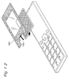
- Fig. 1 is a view showing an example of the next interface for a portable telephone, or the like, and illustrates a state that in order for a liquid crystal display device 20 to be arranged inside the touch- input- function added protective panel 1, for an electronic instrument display window, according to an embodiment of the present invention, the protective panel 1 and the liquid crystal display device 20 are arranged in a casing 19 for an electronic instrument.
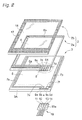
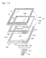
- Fig. 2 is an exploded perspective view illustrating a basic structure of the touch-input-function added protective panel 1 for an electronic instrument display window, according to the embodiment of the present invention.
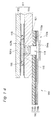
- Fig. 3A is an enlarged sectional side view illustrating a state of the touch-input-function added protective panel 1 for an electronic instrument display window, according to the embodiment of the present invention immediately after an electroconductive adhesive 15 is filled thereinto.
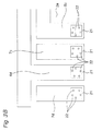
- Fig. 3B is an enlarged plan view of a connection region 8 of the lower surface of an upper electrode sheet 2a showing a state that particles 22 are fixed and arranged by a supporting layer 21 in a region opposite to the region at the peripheral edge of a through hole 9d in Fig. 3A before the electroconductive adhesive 15 of the protective panel 1 is filled.
- 3B is a plan view of a state that the upper electrode sheet 2a is turned upside down and then the lower surface of the upper electrode sheet 2a is directed upwards in order that the situations of the particles 22 and the supporting layer 21 for supporting the particles 22 are well understandable.
- the touch-input-function added protective panel 1 for an electronic instrument display window is constructed to have a transparent and rectangular plate-shaped lower electrode panel 3, the upper electrode sheet 2a, which is transparent and rectangular and is arranged outside of the lower electrode panel 3, a rectangular decorative sheet 2b arranged outside the upper electrode sheet 2a, and an FPC (flexible printed circuit board) 10 arranged inside the lower electrode panel 3.
- the upper electrode sheet 2a which is transparent and rectangular and is arranged outside of the lower electrode panel 3
- a rectangular decorative sheet 2b arranged outside the upper electrode sheet 2a
- FPC flexible printed circuit board
- the lower electrode panel 3 is constructed to have, on the upper surface of a nonflexible, transparent and rectangular protective panel body 3A, a rectangular lower transparent electrode 5 and band-form lower circuits 7a and 7b around the lower transparent electrode 5.
- the upper electrode sheet 2a is constructed to have, on the lower surface of a flexible, rectangular and transparent insulating film, a rectangular upper transparent electrode 4 located at a position opposite to the lower transparent electrode 5, and band-form upper circuits 6a to 6d, 7c and 7d located around the upper transparent electrode 4.
- the circuits 6c and 6d are routing lines for giving outputs from the upper circuits 6a and 6b, respectively, to the outside.
- the circuits 7c and 7d are routing lines for connection to the lower circuits 7a and 7b, respectively.
- the decorative sheet 2b is constructed to have, on a flexible, rectangular and transparent insulating film, a decorative layer 17 having a rectangular frame shape for hiding, by means of its pattern region, each of the lower circuits 7a and 7b of the lower electrode panel 3 and the upper circuits 6a to 6d, 7c and 7d of the upper electrode sheet 2a arranged at the peripheral edge region of the film, and defining a rectangular transparent window section 18.
- the decorative sheet 2b is adhered onto the whole of the front surface (outside surface) of the upper electrode sheet 2a through a transparent adhesive layer 5d (see Fig. 3A ), so as to constitute a movable sheet 2.
- main constituting members each have a rectangular shape.
- the shapes thereof are not limited to the rectangular shape.
- the material of the nonflexible protective panel body 3A of the lower electrode panel 3 may be, for example, a glass plate; a plate of an engineering plastic such as a polycarbonate, polyamide, or polyetherketone plastic; or a plate of plastic such as an acrylic, polyethylene terephthalate, or polybutylene terephthalate; or the like. It is allowable to adhere, onto a surface of such a plate where the lower transparent electrode 5 is to be formed, a film of an engineering plastic such as a polycarbonate, polyamide, or polyetherketone plastic; an acrylic; polyethylene terephthalate; polybutylene terephthalate plastic; or the like, thereby forming the lower electrode panel 3.
- an engineering plastic such as a polycarbonate, polyamide, or polyetherketone plastic
- an acrylic polyethylene terephthalate
- polybutylene terephthalate plastic or the like
- the material of the flexible and transparent insulating film of the upper electrode sheet 2a may be, for example, a film of an engineering plastic such as a polycarbonate, polyamide, or polyetherketone plastic; an acrylic; polyethylene terephthalate; polybutylene terephthalate plastic; or the like.
- an engineering plastic such as a polycarbonate, polyamide, or polyetherketone plastic
- acrylic acrylic
- polyethylene terephthalate polybutylene terephthalate plastic
- the upper electrode sheet 2a and the lower electrode panel 3 are arranged oppositely to each other to make a gap 35 (see Fig. 17 ) between the transparent electrodes 4 and 5, and are bonded to each other, through an adhesive, in individual peripheral edge regions of the upper electrode sheet 2a and the lower electrode panel 3.
- each of the transparent electrodes 4 and 5 is formed into a rectangular form by vacuum vapor deposition, sputtering, ion plating, or CVD: a film of a metal oxide such as tin oxide, indium oxide, antimony oxide, zinc oxide, cadmium oxide, or indium tin oxide (ITO); a composite film made mainly of any one of these metal oxides; or a film of a metal such as gold, silver, copper, tin, nickel, aluminum, or palladium.
- a metal oxide such as tin oxide, indium oxide, antimony oxide, zinc oxide, cadmium oxide, or indium tin oxide (ITO)
- ITO indium tin oxide
- a composite film made mainly of any one of these metal oxides or a film of a metal such as gold, silver, copper, tin, nickel, aluminum, or palladium.
- the upper transparent electrode 4 On the upper electrode sheet 2a, the upper transparent electrode 4 is formed, and further band-form bus bars 6a and 6b are formed around the upper transparent electrode 4 to be partially parallel to each other; the bus bars 6a and 6b are connected to the upper transparent electrode 4 as the upper circuits 6a to 6d, 7c and 7d, and formed by use of a metal such as gold, silver, copper, or nickel, or an electroconductive paste of carbon or the like.
- a metal such as gold, silver, copper, or nickel, or an electroconductive paste of carbon or the like.
- band-form bus bars 7a and 7b extended in a direction orthogonal to the bus bars 6a and 6b are formed, as the lower circuits 7a and 7b, around the lower transparent electrode 5.
- the band-form bus bars 6a, 6b, 7a and 7b can each be formed by a printing method such as screen printing, offset printing, gravure printing, or flexography; a photoresist method; a brush printing method; or the like.
- connection region 8 located at one (the lower end edge in Fig. 2 ) of edge regions of the upper electrode sheet 2a, so as to be collected at the section, which is a single region.
- the bus bars 6a and 6b of the upper electrode sheet 2a are extended to the electrode ends 6d and 6c of the connection region 8, respectively; and further through the electroconductive adhesive 15 (see Fig. 3A , Fig.
- connection holes 16a in an adhesive layer 16 regions (routing lines) 7e and 7f extended from the respective bus bars 7a and 7b of the lower electrode panel 3 are connected to the respective electrode ends 7c and 7d formed, in the connection region 8 of the upper electrode sheet 2a, so as to be parallel to the electrode ends 6d and 6c.
- connection hole inside diameter size of the connection holes 16a in the adhesive layer 16 for connecting these extended regions (routing lines) 7e and 7f, the electrode ends 7c and 7d, and pins 12 and 14 of an FPC 10 to each other through the electroconductive adhesive 15 is equal to the inside diameter size of through holes 9b and 9d
- the connection hole inside diameter size is insufficient for attaining the electrical conduction certainly, and is preferably larger than the inside diameter size of the through holes 9b and 9d, for example, slightly larger than it.
- connection hole inside diameter size of the connection holes 16a in the connection layer 16 for connecting the electrode ends 6c and 6d to pins 11 and 13 of the FPC 10, respectively, through the electroconductive adhesive 15 is equal to the inside diameter size of the through holes 9a and 9c
- the connection hole inside diameter size is insufficient for attaining the electrical conduction certainly, and is preferably larger than the inside diameter size of the through holes 9a and 9c, for example, slightly larger than it. It is necessary to make the inside diameter size of the connection holes 16a at lowest about 1.5 times larger than the inside diameter size of each of the through holes 9a to 9d.
- the through holes 9a to 9d are made, respectively, in the lower electrode panel 3.
- the FPC 10 is formed as the pin-attached FPC 10, wherein the four metallic pins 11 to 14 are stood at a connection side end 10a of the FPC 10, correspondingly to the through holes 9a to 9d.
- the metallic pins 11 to 14 are electrically connected to the electrode ends 6c, 7c, 6d and 7d, respectively, through the electroconductive adhesive 15 not illustrated in Fig. 2 (see the electroconductive adhesive 15 in Fig. 3A and Fig. 4 ).
- a method for the connection of the FPC 10 from the rear surface of the lower electrode panel 3 is disclosed in Patent document 2.
- the structure of the FPC 10 may be a structure as described in the following; however, the structure is not limited thereto: in the connection side end 10a of the FPC 10, metallic pin fixing holes 10g are made in each of a film substrate 10f, and a circuit 10c as an electroconductive region; from the circuit 10c side into the metallic pin fixing holes 10g are inserted the metallic pins 11 to 14, which each have a pin shaft portion (for example, reference number 14b in the metallic pin 14) and a head portion (for example, reference number 14a in the metallic pin 14) formed to have a larger diameter than the outside diameter of this pin shaft portion; and a coverlay film 10b is adhered and bonded onto the circuit 10c and the film substrate 10f to cover the head portions (for example, reference number 14a in the metallic pin 14) of the metallic pins 11 to 14.
- the decorative sheet 2b which has the rectangular transparent window 18, is adhered onto the front surface of the upper electrode sheet 2a.
- the decorative layer 17 is constituted by a pattern region on a single surface of a flexible and transparent insulating film and around the transparent window 18, in other words, the layer 17 is formed to hide the upper circuits 6a to 6d, 7c and 7d, or the lower circuits 7a and 7b, or so on;
- the insulating film may be, for example, a film of an engineering plastic such as a polycarbonate, polyamide, polyetherketone plastic; an acrylic; polyethylene terephthalate; or polybutylene terephthalate plastic; or the like.
- a colored ink which contains a resin as a binder and a pigment or dye in an appropriate color as a colorant, with as the resin being used polyvinyl resins, polyamide resins, polyester resins, polyacrylic resins, polyurethane resins, polyvinyl acetal resins, polyester urethane resins, or alkyd resins.
- an ordinary printing method such as screen printing, offset printing, gravure printing, or flexography. In order to perform multi-color printing or gradation display, offset printing or gravure printing is particularly suitable.
- the decorative layer 17 may be a metallic thin film layer, or a combination of a pattern printed layer with a metallic thin film layer.
- the metallic thin film layer is a layer for representing metallic luster as the decorative layer 17, and is formed by vacuum vapor deposition, sputtering, ion plating, or plating. In this case, the following may be used in accordance with the metallic luster color to be represented: a metal such as aluminum, nickel, gold, platinum, chromium iron, copper, tin, indium, silver, titanium, lead, or zinc; or an alloy or compound of any two or more of these metals.
- the film thickness of the metallic thin film layer is generally set to about 0.05 ⁇ m.
- the decorative sheet 2b is adhered onto the whole of the front surface (outside surface) of the upper electrode sheet 2a through the adhesive layer 5d (see Fig. 3A ), whereby the movable sheet 2 is constructed.
- the surface of the decorative sheet 2b is pushed and pressed downwards with a finger, a pen, or the like, the movable sheet 2 is unified with the finger, the pen, or the like to be bent downwards, so that the transparent electrodes 4 and 5 formed on the respective inside surfaces of the upper electrode sheet 2a and the lower electrode panel 3 are brought into contact with each other.
- the input position is detected.
- the adhesive layer 5d used for the adhesion for example, the following is used: a polyacrylic resin, a polystyrene resin, a polyamide resin, vinyl chloride, vinyl acetate, an acrylic copolymer, or the like.
- the method for forming the adhesive layer 5d may be an ordinary printing method such as screen printing, offset printing, gravure printing, or flexography, or some other method.
- FIG. 3A is an enlarged sectional side view illustrating the state of the tauch-input-function added protective panel 1 according to the embodiment of the present invention immediately after the electroconductive adhesive 15 is filled thereinto.
- the through hole 9d is illustrated as a typical example thereof.
- the features of the embodiment of the present invention are structures as described in the following:
- reference number 16 represents the adhesive layer, which has a frame shape for adhering the upper electrode sheet 2a of the movable sheet 2 and the lower electrode panel 3 to each other in their peripheral edge regions. It is necessary that the individual connection holes 16a, in which the electroconductive adhesive (reference number 15 in Fig. 3A ) is to be injected, are made in the adhesive layer 16, correspondingly to the individual electrode ends 6c, 7c, 6d and 7d in the connection region 8. In other words, the through holes 9a to 9d each made in the lower electrode panel 3 are made so as to be directed and connected to these connection holes 16a.
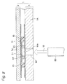
- the electroconductive adhesive 15 is injected into the individual connection holes 16a by means of a dispenser 90 or the like (see Fig. 5 ).
- a dispenser 90 or the like see Fig. 5 .
- the upper electrode sheet 2a of the movable sheet 2 and the lower electrode panel 3 are bonded to each other through the adhesive layer 16.
- the individual connection holes 16a are connected to the individual through holes 9a to 9d in the connection region 8, and are further made to be partitioned by the adhesive layer 16, the upper electrode sheet 2a of the movable sheet 2, and the lower electrode panel 3.
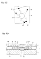
- Fig. 3C is an enlarged plan view of the connection region of the upper circuit 7d in Fig. 3B .
- white arrows each represent a flow of the electroconductive adhesive 15 injected from the through hole 9d in the lower electrode panel 3.
- Fig. 3C shows that the electroconductive adhesive 15 flows, as represented by the white arrows, through a space defined between the particles 22, which constitute an example of the dot spacers 30, so that the electroconductive adhesive 15 is filled into the connection holes 16a.
- An example of the adhesive layer 16 is a double faced adhesive tape which has such a rectangular frame shape that regions for attaining inputs while a screen of the liquid crystal display device 20 or the like is seen through (the transparent window 18 in Fig. 2 ) are punched out, and is formed by punching out at least the individual connection holes 16a in portions of the rectangular frame shape.
- the adhesive layer 16 may be an adhesive layer formed by painting an insulating adhesive, for example, an aqueous or acrylic printing paste or some other printing paste.
- the size of each of the gaps in the individual connection holes 16a and between the lower electrode panel 3 upper surface at the peripheral edges of the through holes 9a to 9d and the movable sheet 2 is maintained (see Fig. 3A ), thereby making it possible to fill the electroconductive adhesive 15 smoothly from the individual through holes 9a to 9d into every portion of the individual connection holes 16a in the adhesive layer 16.
- the connection reliability of the FPC 10 which depends on the filling degree of the electroconductive adhesive 15, is improved.
- the injection of the electroconductive adhesive 15 can be attained in the state that no depression is generated in the movable sheet 2 (see Fig. 5 ), so that the external appearance quality of the protective panel 1 is improved.
- the particles 22 can resist the shrinkage stress of the electroconductive adhesive 15.
- depressions in the movable sheet 2 are decreased so that the external appearance quality of the protective panel 1 can be improved.
- the filled electroconductive adhesive 15 is a product wherein electroconductive fillers are incorporated into a binder made of a silicone, epoxy, acrylic, or urethane resin.
- the electroconductive filler may be a powder of an electroconductive metal such as silver, gold, copper, nickel, platinum, or palladium; a filler wherein an inorganic insulator such as alumina or glass, an organic polymer such as polyethylene, polystyrene, or divinylbenzene, or the like is used as an electroconductive filler nucleus material, and any surface of the nucleus material is coated with an electroconductive layer of gold, nickel, or the like; or a filler wherein any surface of the nucleus material is coated with an electroconductive layer of carbon, graphite, or the like.
- the electroconductive adhesive 15 may be of either a thermosetting type or an ultraviolet curable type, and may be of either a one-component type or a two-component type.
- the electroconductive filler may be a filler in the form of flakes, spheres, short fibers, or the like.
- the method for painting the electroconductive adhesive 15 may be a dispenser method or the like.
- the individual dots of the dot spacers 30, as an example of which the particles 22 function, may be formed, for example, by fixing and bonding the particles 22 onto the movable sheet 2 as illustrated in Fig. 3A .
- the particles 22 are particles having a particle diameter substantially equal to the size between the movable sheet 2 and the lower electrode panel 3, as illustrated in Fig. 3A .
- the particle 22 is preferably made spherical.
- the length sizes of the particle along the length and breadth directions thereof are substantially equal to the thickness size thereof; thus, in any state the particles 22 are fixed and bonded to the movable sheet 2, the size of the gaps between the lower electrode panel 3 upper surface at the peripheral edges of the through holes 9a to 9d and the movable sheet 2 and further in the individual connection holes 16a can be certainly kept at a predetermined value (for example, a size substantially equal to the particle diameter of the particle 22) (spacer function can be fulfilled).
- the thickness size thereof is far smaller than the length sizes of the flake-form particles along the length and breadth directions (the thickness size is smaller than the gap size).
- the gap size may not be locally kept at the predetermined value.
- the thickness of the adhesive layer 16 is, for example, 50 ⁇ m, it is preferred to set the average particle diameter of the particles 22 into the range of 75 ⁇ 10 ⁇ m (65 to 85 ⁇ m).
- the distribution of the particles 22 is set into, for example, 10 particles/mm 2 .
- the average particle diameter of the particles 22 is not always set into the range of 65 to 85 ⁇ m.
- the average particle diameter of the particles 22 is also varied. In other words, if the average particle diameter of the particles 22 is too small for the thickness of the adhesive layer 16, the movable sheet 2 cannot be supported. On the other hand, if the average particle diameter of the particles 22 is too large for the thickness of the adhesive layer 16, irregularities are generated in the surface of the movable sheet 2.
- the matter that the average particle diameter of the particles 22 ranges from 75 ⁇ 10 ⁇ m (65 to 85 ⁇ m) is an example, and is a numerical example when the thickness of the adhesive layer 16 is 50 ⁇ m.
- the ratio is from 1.3 to 1.7. If this ratio is smaller than 1.3, the movable sheet 2 cannot be supported. On the other hand, if this ratio is more than 1.7, irregularities are generated in the surface of the movable sheet 2.
- the number of the particles the following can be described: if the number of the particles is too large, the electroconductive adhesive 15 is not easily filled; on the other hand, if the number of the particles is too small, the movable sheet 2 cannot be supported. Thus, in an example, a density of 10 particles/mm 2 is preferred.
- the fixing and bonding of the particles 22, which has the spacer function, onto the movable sheet 2 can be attained by the supporting layer 21, which is, for example, rectangular (see Fig. 3A and Fig. 3B ).
- the supporting layer 21 is formed specifically by painting, into a predetermined area (for example, the connection region of the band-form upper circuits 6a to 6d, 7c and 7d) of the movable sheet 2, a slurry wherein the particles 22 are numerously incorporated into a binder of a silicone, epoxy, acrylic, or urethane resin.
- the method for the painting may be a dispenser method, a screen printing method, or the like.
- a well-known particle-fixing/bonding-technique may be adopted besides the means based on the supporting layer 21.
- the thickness of the supporting layer 21 is 20 ⁇ m
- the diameter of the particles 22 is 75 ⁇ m
- the inside diameter of the through holes is 1.5 mm.
- the supporting layer 21 that is, the necessity of fixing the particles 22
- the particles 22 are not fixed onto the movable sheet 2 by means of the supporting layer 21 (that is, the particles 22 are not fixed onto the movable sheet 2), the following is unfavorably caused even when the particles 22 are evenly arranged at the peripheral edge of the through hole 9d as illustrated in Fig. 6A and Fig.
- the connection reliability falls.
- the particles 22 are fixed onto positions at the peripheral edge of the through hole 9d by means of the supporting layer 21 (that is, the particles 22 are fixed onto the movable sheet 2)
- the following can be attained even when the electroconductive adhesive 15 is injected from the through hole 9d into the gaps of the individual connection holes 16a: by the electroconductive adhesive 15, the particles 22 are not shifted from the positions at the peripheral edge of the through hole 9d, so that the size of the gap of each of the connection holes 16a can be certainly kept at the predetermined value at the peripheral edge of the through hole 9d.
- the electroconductive adhesive 15 can go around the particles 22, so that the space 37 does not remain between the electroconductive adhesive 15 and the adhesive layer 16.
- the connection reliability can be made high.
- the shape of the supporting layer 21 is not limited to a rectangular shape, and may be any shape.
- Fig. 3D is an enlarged plan view of the connection region of the same upper circuit 7d as in Fig. 3C in a case where the supporting layer 21 is a supporting layer 21A in a rectangular frame shape.
- the particles 22 are fixed to a region of the lower electrode panel 3 which is opposite to the through hole 9d (the central region of the supporting layer 21)
- an obstacle is caused at the time of filling the electroconductive adhesive 15 from the through hole 9d into the connection holes 16a.
- the adhesive 15 may be unevenly injected.
- the particles 22 are set not to be fixed to a region of the lower electrode panel 3 opposite to the through hole 9d (the central region of the supporting layer 21).
- the particles 22 are fixed to a region of the lower electrode panel 3 which is opposite to the region at the peripheral edge of the through hole 9d (a region around the central region of the supporting layer 21).
- the particles 22 are easily arranged also into the central region of the supporting layer 21; therefore, as illustrated in Fig.
- the particles 22 can be certainly prevented from being fixed to the central region of the supporting layer 21A.
- the supporting layer 21A can easily be formed by printing a pattern having such a shape.
- the pattern shape is not limited to any rectangular frame shape, and may be any pattern shape as far as the pattern shape makes it possible that the particles 22 are not arranged in the central region thereof.
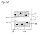
- the pattern shape may be constituted by two rectangular-band-form supporting layers 21B and 21B arranged to leave a gap 21b in a region corresponding to the central region of the supporting layer 21A.
- the pattern shape is not limited to any pattern printed so as to exclude the central region of the supporting layer 21.
- the following manner may be used: a manner of printing a rectangle with an ink wherein the particles 22 are evenly dispersed in a binder, so as to form the supporting layer 21, adding compressed air lightly to the central region of the supporting layer 21 before the ink is dried, so as to shift the ink not dried from the central region of the supporting layer 21 to the peripheral region thereof, thereby making the rectangular hole 21a.
- the supporting layer 21 When the supporting layer 21 is laid, it is preferred to render the supporting layer 21 an electroconductive layer. Specifically, besides the particles 22, which have the spacer function, many fine electroconductive fillers are incorporated into the binder, which constitutes the supporting layer 21, inside the supporting layer 21, thereby giving electroconductivity to the supporting layer 21 itself. Under such a condition, the filler-incorporated mixture is painted into a predetermined area of the movable sheet 2. When the supporting layer 21 is not electroconductive, the individual electrode ends 6c, 7c, 6d and 7d of the movable sheet 2 cannot attain electrical connection in their regions covered with the supporting layer 21. Thus, about the size of the area where the supporting layer 21 is formed, design flexibility is small.
- the electroconductive filler may be a powder of an electroconductive metal such as silver, gold, copper, nickel, platinum, or palladium; a filler wherein an inorganic insulator such as alumina or glass, an organic polymer such as polyethylene, polystyrene, or divinylbenzene, or the like is used as a nucleus material, and any surface of the nucleus material is coated with an electroconductive layer of gold, nickel, or the like; or a filler wherein any surface of the nucleus material is coated with carbon, graphite, or the like.
- the electroconductive filler may be a filler in the form of flakes, spheres, short fibers, or the like.
- the electroconductive particles may be a powder of an electroconductive metal such as silver, gold, copper, nickel, platinum, or palladium; a filler wherein an inorganic insulator such as alumina or glass, an organic polymer such as polyethylene, polystyrene, or divinylbenzene, or the like is used as an electroconductive particle nucleus material, and any surface of the nucleus material is coated with an electroconductive layer of gold, nickel, or the like; a filler wherein any surface of the nucleus material is coated with an electroconductive layer of carbon, graphite, or the like; or other particles.
- an electroconductive metal such as silver, gold, copper, nickel, platinum, or palladium
- a filler wherein an inorganic insulator such as alumina or glass, an organic polymer such as polyethylene, polystyrene, or divinylbenzene, or the like is used as an electroconductive particle nucleus material, and any surface of the nucleus material is coated with an electroconductive layer of gold
- the connection performance between the region 7f extended from the bus bar 7b of the lower electrode panel 3 and the electrode end 7d of the movable sheet 2 is stabilized for the following reason: even when the heating/drying shrinkage or normal-temperature-curing shrinkage of the electroconductive adhesive 15 causes a gap to be generated between the electroconductive adhesive 15 and the extended region 7f or electrode end 7d, electrical connection is attained through the supporting layer 21 and the particles 22 between the upper and lower circuits.
- the present invention is not limited to any embodiment wherein the particles 22 are fixed onto the lower surface side of the movable sheet 2 as illustrated in Fig. 3A .
- the present invention may be made into an embodiment wherein the particles 22 are fixed on the upper surface side of the lower electrode panel 3 by a supporting layer 21C.
- This supporting layer 21C has, in the central region thereof, through holes 21c connected to the respective through holes 9a to 9d.
- the size thereof is made equal to or more than the inside diameter of the through holes 9a to 9d.
- the upper limit value of the inside diameter of the through holes 21 is preferably 3 mm. If the inside diameter of the through holes 21 is more than 3 mm, the distance between the transparent window and the panel outer edge becomes large so that the frame is not easily made narrow.
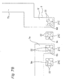
- Fig. 7C is an enlarged plan view of the region 7f, which is a region extended from the lower circuit 7b in a case where the supporting layer 21C having the through holes 21c is fixed onto the upper surface side of the lower electrode panel 3.
- white arrows each represent a flow of the electroconductive adhesive 15 injected from the through hole 9d in the lower electrode panel 3.
- Fig. 7C shows that the electroconductive adhesive 15 flows as represented by the white arrows between the particles 22, which constitute the dot spacers 30, so that the electroconductive adhesive 15 is filled into the connection holes 16a.
- the supporting layer 21C is beforehand formed to have the through holes 21c the inside diameter of which is larger than that of the through hole 9d. In this case, it is unnecessary to make the through holes 21c afterwards. No wastes are generated when the supporting layer 21 and the particles 22 are removed while the through hole is made. Thus, the case is preferred.
- the particles 22 may be fixed by the two supporting layers 21, which are upper and lower supporting layers. In this case, it is unnecessary that all the particles 22 are fixed onto both of the lower surface side supporting layer 21 of the movable sheet 2 and the upper surface side supporting layer 21 of the lower electrode panel 3; thus, it is sufficient for the case that the particles are fixed onto at least one of the supporting layers 21.
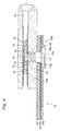
- Fig. 8 is illustrated an example wherein the supporting layer 21 is arranged on the lower surface side of the movable sheet 2 and the supporting layer 21C is arranged on the upper surface side of the lower electrode panel 3.
- an anchor effect is obtained.
- the particles 22 sink slightly into the lower electrode panel 3
- physical connection between the movable sheet 2 onto which the particles 22 are fixed and bonded, and the lower electrode panel 3 opposite thereto is stabilized.
- the particles 22 fixed and bonded onto the movable sheet 2 sink slightly into the lower electrode panel 3
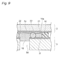
- physical connection of the circuits (the lower circuit 7f in Fig. 9 ) is stabilized in the lower electrode panel 3, so that the circuits less exfoliate.
- the same anchor effect is obtained when the particles 22 sink slightly into the movable sheet 2.
- the sinking amount of the particles 22 into the opposite member is decreased. Instead of the decrease, the contact area with the opposite member is increased so that the same effect is obtained.
- the present invention is not limited to any product wherein the supporting layer 21 is arranged for each of the upper circuits 7d, 6d, 7c and 6d.
- the present invention may be a product wherein a single supporting layer 21, 21A, 21B or 21C is arranged for the plural upper circuits 7d, 6d, 7c and 6d.
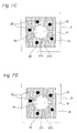
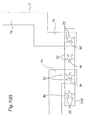
- Fig. 10A it is allowable to arrange a rectangular-band-form supporting layer 21D onto the lower surface side of the movable sheet 2 to extend over the plural upper circuits 7d, 6d, 7c and 6d adjacent to one another, and fix the particles 22 onto each of the upper circuits 7d, 6d, 7c and 6d.
- This Fig. 10A is a plan view of a state that the upper electrode sheet 2a is turned upside down and then the lower surface of the upper electrode sheet 2a is directed upwards as the situation of the particles 22 and the supporting layer 21D supporting the particles 22 is well understandable.
- the rectangular-band-form supporting layer 21D is arranged in such a manner that the connection region of the four upper circuits 7d, 6d, 7c and 6d is covered with the single layer 21D; however, of course, the arrangement is not limited thereto.
- the single rectangular-band-form supporting layer 21D may be arranged in such a manner that the connection region of two or three upper circuits is covered therewith.
- a rectangular-band-form supporting layer 21E onto the upper surface side of the lower electrode panel 3 to extend over the plural extended regions 7e and 7f adjacent to each other, which are regions extended from the bus bars 7a and 7b, respectively, that is, to extend over the upper surface side positions of the lower electrode panel 3 that are at the peripheral edges of the through holes 9a, 9b, 9c and 9d, and fix the particles 22 to a position at the peripheral edge of each of the through holes 9a, 9b, 9c and 9d.
- the rectangular-band-form supporting layer 21E is arranged in such a manner that positions at the peripheral edges of the four through holes 9a, 9b, 9c and 9d are covered with the single layer 21E; however, of course, the arrangement is not limited thereto.
- the single rectangular-band-form supporting layer 21E may be arranged in such a manner that positions at the peripheral edges of two or three through holes are covered therewith.
- the spacers 30 are not limited to the particles 22, and may be prismatic spacers, or columnar spacers as described below, or the like.
- the spacers 30 may have any shape as far as the spacers can exhibit each of a function of permitting gaps between regions at the peripheral edges of the through holes 9a to 9d to be kept to such a degree that depressions in the movable sheet are decreased, and a function of not hindering the electroconductive adhesive 15 injected from the through holes 9a to 9d from being filled into the connection holes 16a.
- the material thereof is preferably electroconductive in the same manner as the particles 22.
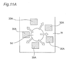
- Fig. 11A and Fig. 11B are, respectively, an enlarged plan view and a sectional side view illustrating an example wherein plural prismatic spacers 30A are fixed in the region 7f extended from the lower circuit 7b in Fig. 2 without using the particles 22.
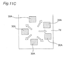
- Fig. 11C is a plan view illustrating an example wherein the plural prismatic spacers 30A are fixed in a region of the upper circuit 7d in Fig. 2 which is opposite to the region at the peripheral edge of the through hole 9d without using the particles 22 in the same manner as in Fig. 11A .
- each of the spacers 30A may be formed by a pattern of, for example, a synthetic resin (by, for example, screen printing).
- the used synthetic resin is preferably a UV curable resin or a two-component curable resin. Since the resin does not contain any solvent, the thickness can be maintained with high precision.
- the plural spacers 30 are fixed and arranged between the upper surface, at the peripheral edges of the through holes 9a to 9d, of the lower electrode panel 3 of the touch-input-function added protective panel 1 and the upper electrode sheet 2a and further in the individual connection holes 16a in the adhesive layer 16, so as to be separated from one another.
- the electroconductive adhesive 15 is filled into the connection holes 16a, the gap interval of which is maintained by the spacers 30. For this reason, the injection of the electroconductive adhesive 15 can be smoothly filled into every portion of each of the connection holes 16a in the adhesive layer 16 for bonding the lower electrode panel 3 and the upper electrode sheet 2a.
- the electroconductive adhesive 15 is certainly filled into the connection holes 16a, and further the following can be electrically connected to one another with certainty: the electrodes 6c, 7c, 6d and 7d of the upper electrode sheet 2a, or the electrodes 7e and 7f of the lower electrode panel 3, which face the connection holes 16a; the electroconductive adhesive 15 in the connection holes 16a; and the pins 11, 12, 13 and 14 of the FPC 10, which are inserted into the through holes 9a to 9d connected to the connection holes 16a.
- the connection reliability of the pin-attached FPC 10 which depends on the filling degree of the electroconductive adhesive 15, is improved.
- the electroconductive adhesive 15 is filled from the through holes 9a to 9d into the connection holes 16a, the gap interval of which is maintained by the spacers 30, so that the injection of the electroconductive adhesive 15 can be attained in the state that no depression is generated in the movable sheet 2, which is a laminated film of the upper electrode sheet 2a and the decorative sheet 2b.
- the external appearance quality of the protective panel 1 is improved.
- the spacers 30 can resist the shrinkage stress.
- depressions in the movable sheet 2 are decreased so that the external appearance quality of the protective panel 1 is improved.
- An ITO film of 20 nm thickness was formed on the whole of a surface of a PET film of 0.1 mm thickness as a lower transparent electrode forming substrate by sputtering, and the peripheral edge region of the ITO film was removed to prepare a lower transparent electrode 5 in the form of a rectangle having a large width.
- Bus bars 7a and 7b arranged to two sides of the lower transparent electrode 5 that were opposite to each other along the traverse direction thereof, and routing lines 7e and 7f for giving outputs from the respective bus bars to the outside were each formed by screen printing using a silver paste.
- a substrate-free transparent adhesive of 0.025 mm thickness was used to adhere an acrylic plate having the same length and width as the PET film and a thickness of 0.7 mm, as a protective panel body 3A, onto the surface of the PET film opposite to the surface thereof on which the lower transparent electrode 5 was formed. Thereafter, in the edge region thereof were made by drilling four through holes 9a, 9b, 9c and 9d of 1.5 mm inside diameter wherein metallic pins 11 to 14 of a pin-attached FPC 10, which will be described later, were to be inserted. In this way, a lower electrode panel 3 was yielded.
- a PET film having the same length and width as the lower electrode panel 3 and a thickness of 125 ⁇ m was used, and an ITO film of 20 nm thickness was formed on the whole of a surface thereof by sputtering. The peripheral edge region of the ITO film was removed to prepare an upper transparent electrode 4 in the form of a rectangle having a large width.
- Bus bars 6a and 6b arranged to two sides of the upper transparent electrode 4 that were opposite to each other along the lengthwise direction thereof, and routing lines 6c and 6d (thickness: 35 ⁇ m) for giving outputs from the respective bus bars 6a and 6b to the outside were each formed by screen-printing a silver paste wherein many electroconductive fillers made of a silver powder (diameter: 10 ⁇ m) in the form of fine flakes were incorporated into a binder made of a polyester resin. In this way, an upper electrode sheet 2a was yielded.
- a hard coat film of a PET substrate having the same length and width as the lower electrode panel 3 and a thickness of 0.075 mm was used, and a decorative layer 17 having a transparent window section 18 was formed onto its surface opposite to its hard coat surface by gravure printing, so as to yield a decorative sheet 2b. Thereafter, the decorative layer side surface of the decorative sheet 2b was adhered onto the surface of the upper electrode sheet 2a opposite to the transparent electrode side surface thereof through a substrate-free transparent adhesive 5d of 0.025 mm thickness. In this way, a movable sheet 2 was yielded.
- plural dot spacers 30 were formed and arranged at positions opposite to regions, at the peripheral edges of the through holes 9a to 9d, of the upper surface of the lower electrode panel 3, so as to be separated from one another.
- electroconductive fillers made of a silver powder (diameter: 10 ⁇ m) in the form of fine flakes were incorporated into a binder made of a polyester resin to prepare a silver paste, and then to the silver paste were further added particles 22 having a spacer function and made of a nickel powder (particle diameter: 75 ⁇ m).
- the resultant was painted by a dispenser method.
- the nickel particles 22 were fixed by a supporting layer 21 made of the silver paste, so as to turn to individual dots of the dot spacers 30.
- the thickness of the supporting layer 21 itself, which was made of the silver paste, was 35 ⁇ m, and the portions to which the nickel particles 22 were fixed and bonded were projected by 40 ⁇ m.
- the lower electrode panel 3 and the movable sheet 2 were arranged to be opposite to each other in such a manner that the electrodes 5 and 4 formed on the elements 3 and 2, respectively, were made apart from each other. These were adhered onto each other through a frame-form double faced adhesive tape (thickness: 50 ⁇ m) (adhesive layer 16) obtained by punching out a region of the transparent window 18 and the individual connection holes 16. The resultant was then cut along the inside circumference edge of the decorative layer 17. By the adhesion, a gap having a thickness of 50 ⁇ m was made between the upper surface of the lower electrode panel 3 at the peripheral edges of the through holes 9a to 9d and the upper electrode sheet 2a. This gap was maintained by the plural dot spacers 30.
- the dot spacers 30 were 25 ⁇ m larger than the distance between the lower electrode panel 3 and the movable sheet 2; thus, the particles 22 constituting the dot spacers 30 pressed the lower electrode panel 3 so that an anchor effect for the lower electrode panel 3 was exhibited.
- connection side end 10a of an FPC 10 wherein a silver paste was used to form a circuit, as an electroconductive section, on a surface of a polyimide film of 0.075 mm thickness
- four metallic-pin-fixing holes of 2.0 mm inside diameter were made by drilling.
- metallic pins 11 to 14 each having a pin shaft of 1.8 mm diameter and 1 mm length and a pin head portion of 2.8 mm diameter from the circuit side surface of the FPC 10.
- a polyimide film (coverlay film 10b) of 0.05 mm thickness was adhered thereto so as to cover the circuit of the FPC 10 and the head portions of the metallic pins 11 to 14 (for example, reference number 14a in the metallic pin 14) . In this way, the pin-attached FPC 10 was yielded.
- an ink of the electroconductive adhesive 15 was injected into the through holes 9a to 9d made in the lower electrode panel 3 by a dispenser, and then the metallic pins 11 to 14 of the pin-attached FPC 10 were inserted into the through holes 9a to 9d from the inlets thereof.
- This electroconductive adhesive 15 was an agent wherein a flake-form silver powder having a particle diameter of 10 ⁇ m was incorporated into a binder made of a silicone resin.
- Working Example 2 The same process as in Working Example 1 was carried out except that in Working Example 2, the dot spacers 30 were further formed on the upper surface of the lower electrode panel 3 at the peripheral edges of the through holes 9a to 9d.
- Working Example 3 was an example wherein as illustrated in Fig. 8 , the dot spacers 30 were fixed onto the upper surface of the lower electrode panel 3 at the peripheral edges of the through holes 9a to 9d and the upper electrode sheet 2a.
- the plural dot spacers 30 were fixed and arranged between the upper surface of the lower electrode panel 3 at the peripheral edges of the through holes 9a to 9d and the upper electrode sheet 2, so as to be separated from one another. From the through holes 9a to 9d, the electroconductive adhesive 15 was filled into the gap maintained by the dot spacers 30.
- the protective panel 1 was excellent in the connection reliability of the FPC 10 and the external appearance quality thereof.
- the touch-input-function added protective panel for an electronic instrument display window is excellent in reliability of its FPC connection region, and is useful for a portable information terminal such as a PDA (personal digital assistance) or a handy terminal, an OA (office automation) instrument such as a copying machine or a facsimile, a smart phone, a portable telephone, a portable game instrument, an electronic dictionary, a car navigation system, a small-sized PC (personal computer), any one of various home electrical appliances, or the like.
Landscapes
- Engineering & Computer Science (AREA)
- Theoretical Computer Science (AREA)
- General Engineering & Computer Science (AREA)
- Human Computer Interaction (AREA)
- Physics & Mathematics (AREA)
- General Physics & Mathematics (AREA)
- Computer Hardware Design (AREA)
- Manufacturing & Machinery (AREA)
- Microelectronics & Electronic Packaging (AREA)
- Position Input By Displaying (AREA)
- Push-Button Switches (AREA)
Abstract
Description
- The present invention relates to a touch-input-function added protective panel for an electronic instrument display window which is used for a portable information terminal such as a PDA (personal digital assistance) or a handy terminal, an OA (office automation) instrument such as a copying machine or a facsimile, a smart phone, a portable telephone, a portable game instrument, an electronic dictionary, a car navigation system, a small-sized PC (personal computer), any one of various home electrical appliances, or the like, and is excellent in reliability of its FPC connection region.
- A casing in an electronic instrument, such as a portable telephone or a smart phone, is generally made of a combination of a front surface casing and a rear surface casing each made of a synthetic resin. Specifically, a protective panel is fixed onto the front surface of the front casing by melt-bonding or the like to protect a liquid crystal display window. As this protective panel, conventionally, a panel made of a transparent and colorless resin has been hitherto used. However, as electronic instruments have been made decorative, a decoration, such as trimming, has been applied thereto by printing.
- In recent years, about portable telephones, a
protective panel 101 having an input device function, as illustrated inFig. 12 , has been expected as the next interface. The interface is disclosed in, for example,Patent document 1. - About the touch-input-function added
protective panel 101 for an electronic instrument display window, a description will be made in more detail, using an exploded view ofFig. 13 . InFig. 13 , the touch-input-function addedprotective panel 101 for an electronic instrument display window is a panel equipped with alower electrode panel 103 having, on the upper surface of a nonflexible protective panel body, a lowertransparent electrode 105, andlower circuits transparent electrode 105; anupper electrode sheet 102a having, on the lower surface of a flexible and transparent insulating film, an uppertransparent electrode 104 located at a position opposite to the lowertransparent electrode 105, andupper circuits 106a to 106d, 107c and 107d located around the uppertransparent electrode 104; and adecorative sheet 102b having, in a flexible and transparent insulating film, adecorative layer 117 for hiding thelower circuits 107a an 107b and theupper circuits 106a to 106d, 107c and 107dby a pattern and forming atransparent window section 118. - On the inside surface of the
upper electrode sheet 102a and that of thelower electrode panel 103, ITO (indium tin oxide) pieces, or the like are formed by sputtering or vacuum vapor deposition in a rectangular form as thetransparent electrodes upper electrode sheet 102a are formed band-form bus bars transparent electrode 104 and are in parallel to each other. On thelower electrode panel 103 are formed band-form bus bars bus bars 106a and 10106b and are connected to thetransparent electrode 105. About theindividual bus bars connection section 108 located at an edge region of theupper electrode sheet 102a, and then collected at the section, which is a single region. - The
decorative sheet 102b is adhered onto the whole of the front surface (outside surface) of theupper electrode sheet 102a (hereinafter, a laminated film of theupper electrode sheet 102a and thedecorative sheet 102b will be called a movable sheet 102). When the surface of thedecorative sheet 102b is pressed with a finger, a pen, or the like, themovable sheet 102 is, in an integrated manner, bent down so that the respectivetransparent electrodes upper electrode sheet 102a and thelower electrode panel 103, are brought into contact with each other. In this way, the input position is detected. - In
Fig. 13 , throughholes 109a to 109d are made in parallel to the Z direction in theconnection section 108 of thelower electrode panel 103, so as to correspond toindividual electrode ends connection section 108, unlike the touch-input-function addedprotective panel 101 for an electronic instrument display window described inPatent document 1. Correspondingly to these throughholes 109a to 109d, fourmetallic pins 112 to 114 are stood at aconnection side end 110a of an FPC (flexible printed circuit board) 110. Themetallic pins 111 to 114 are electrically connected to theelectrode ends Fig. 13 (seereference number 115 inFig. 14 ). A method for the connection of the FPC from the rear surface of thelower electrode panel 103 is disclosed inPatent document 2. - In the pin-attached
FPC 110 described inPatent document 2, at theconnection side end 110a of theFPC 110, metallicpin fixing holes 110g are made in each of afilm substrate 110f, and acircuit 110c as an electrically conductive section. Into the metallicpin fixing holes 110g are inserted themetallic pins 111 to 114, which each have a pin shaft portion and a head portion formed to have a larger diameter than the outside diameter of this pin shaft portion, from thecircuit 110c side. Acoverlay film 110b is adhered and bonded onto thecircuit 110c and thefilm substrate 110f so as to cover the head portions (for example,reference number 114a inFig. 14 ) of themetallic pins 111 to 114 (seeFig. 14 ). -
Reference number 116 inFig. 14 represents an adhesive layer for adhering theupper electrode sheet 102a of themovable sheet 102 and thelower electrode panel 103 to each other in their peripheral edge regions. In theadhesive layer 16 are madeindividual connection holes 121, to which the electroconductive adhesive (seereference number 115 inFig. 14 ) is to be injected, so as to correspond to theindividual electrode ends connection section 108. -
- Patent document 1: International Publication
2005/064451 pamphlet - Patent document 2: International Publication
2006/077784 pamphlet - However, when the
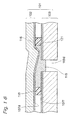
electroconductive adhesive 115 is injected from theconnection hole 121 in each of theelectrode ends connection hole 121, which is a hollow region in theadhesive layer 116, naturally, a void (air gap) is made between themovable sheet 102 and the lower electrode panel 103 (seeFig. 15 ), and further themovable sheet 102 is, in an integrated manner, easily bent down; therefore, the size of the interval between themovable sheet 102 and thelower electrode panel 103 is easily varied. Accordingly, when theelectroconductive adhesive 115 is injected therein, themovable sheet 102 is depressed over each of theconnection holes 121, as illustrated inFig. 16 , so that theelectroconductive adhesive 115 cannot be sufficiently injected. The connection with theelectroconductive adhesive 115 in theconnection section 108 depends on the filling degree of theelectroconductive adhesive 115. In particular, in a case where, as seen in theelectrode ends electrode ends form bus bars electroconductive adhesive 115 cannot be sufficiently filled as described above, the connection reliability of the pin-attachedFPC 110 falls. - The
electroconductive adhesive 115 is cured by heating and drying, or curing at normal temperature (moisture curing, anaerobic curing, or two-component curing) ; thus, when theelectroconductive adhesive 115 is cured in the state that themovable sheet 102 over theindividual connection holes 121 are depressed as described above so that theelectroconductive adhesive 115 cannot be sufficiently injected therein, the depressions in themovable sheet 102 are maintained. As a result, the external appearance quality of the touch-input-function addedprotective panel 101 becomes low for the following reason: about theprotective panel 101, the whole of the front surface of themovable sheet 102 is to be an outer package of an electronic instrument, so that the depressions in themovable sheet 102 are to exist. - Even in a case where no depression is generated at the time of the injection of the
electroconductive adhesive 115, theelectroconductive adhesive 115 shrinks when heated and dried or cured at normal temperature, thereby generating depressions in themovable sheet 102 to decline the external appearance quality of theprotective panel 101. - An object of the present invention is to resolve the issues as described above in the prior art, and provide a touch-input-function added protective panel for an electronic instrument display window which is excellent in connection reliability of its FPC, or the external appearance quality.
- In order to attain the object, the present invention is constructed as follows:
- According to a first aspect of the present invention, there is provided a touch-input-function added protective panel for an electronic instrument display window, comprising:
- a lower electrode panel having, on an upper surface of a nonflexible protective panel body, a lower transparent electrode and a lower circuit located around the lower transparent electrode;
- an upper electrode sheet arranged on an upper side of the lower electrode panel, having, on a lower surface of a flexible and transparent insulating film, an upper transparent electrode located at a position opposite to the lower transparent electrode and an upper circuit located around the upper transparent electrode, and further bonded, at its peripheral edge region, to the lower electrode panel through an adhesive layer so as to form an inter-electrode gap between the upper transparent electrode and the lower transparent electrode;
- a decorative sheet arranged on an upper side of the upper electrode sheet, having, in at least one surface of a flexible and transparent insulating film, a decorative layer that hides the lower circuit and the upper circuit and forms a transparent window section, and further adhered onto an upper surface of the upper electrode sheet; and
- an FPC that takes out an electrical signal through a pin inserted into a through hole made in the lower electrode panel,
- wherein the adhesive layer has a connection hole connected to the through hole, plural spacers are fixed and arranged in the connection hole and between the upper surface, at the peripheral edge of the through hole, of the lower electrode panel and the upper electrode sheet, so as to be separated from one another, and an electroconductive adhesive is filled from the through hole into the connection hole, a gap interval of an inside of which is maintained by the spacers.
- According to a second aspect of the present invention, there is provided the touch-input-function added protective panel for an electronic instrument display window according to the first aspect, wherein the spacers are dot spacers, and dots of the dot spacers are each fixed and bonded to at least one of the lower electrode panel and the upper electrode sheet.
- According to a third aspect of the present invention, there is provided the touch-input-function added protective panel for an electronic instrument display window according to the first aspect, wherein the spacers are dot spacers, and dots of the dot spacers are each a particle fixed and bonded to at least one of the lower electrode panel and the upper electrode sheet.
- According to a fourth aspect of the present invention, there is provided the touch-input-function added protective panel for an electronic instrument display window according to the third aspect, wherein the particle is fixed and bonded by fixing a supporting layer that fixes the particle, to at least one of the lower electrode panel and the upper electrode sheet.
- According to a fifth aspect of the present invention, there is provided the touch-input-function added protective panel for an electronic instrument display window according to the fourth aspect, wherein the supporting layer is a layer having electroconductivity.
- According to a sixth aspect of the present invention, there is provided the touch-input-function added protective panel for an electronic instrument display window according to any one of the first to fifth aspects, wherein the spacers have electroconductivity.
- According to a seventh aspect of the present invention, there is provided the touch-input-function added protective panel for an electronic instrument display window according to any one of the third to fifth aspects, wherein the particle is spherical.
- According to an eighth aspect of the present invention, there is provided the touch-input-function added protective panel for an electronic instrument display window according to any one of the first to fifth aspects, wherein a height size of the spacers is larger than a gap interval size of the connection hole that is maintained, in the connection hole in the adhesive layer, by the spacers.
- According to a ninth aspect of the present invention, there is provided the touch-input-function added protective panel for an electronic instrument display window according to any one of the first to fourth aspects, wherein the spacers are arranged around a position of the upper surface of the lower electrode panel which corresponds to an inside of the through hole, so as to be in positions except the position, which corresponds to the inside of the through hole.
- According to a tenth aspect of the present invention, there is provided the touch-input-function added protective panel for an electronic instrument display window according to the fourth or fifth aspect, wherein the supporting layer has a frame shape having, at a position of the upper surface of the lower electrode panel which corresponds to an inside of the through hole, a through hole, and the particles are fixed to regions of the supporting layer except the through hole in the supporting layer, whereby the particles are arranged around the position corresponding to the inside of the through hole. Effects of the Invention
- In the touch-input-function added protective panel according to the present invention, between the upper surface, at the peripheral edge of a through hole, of its lower electrode panel and its upper electrode sheet and further in the connection hole in its adhesive layer, plural spacers are fixed and arranged so as to be separated from one another, and an electroconductive adhesive is filled from the through hole into the connection hole, the gap interval of which is maintained by the spacers. For this reason, the injection of the electroconductive adhesive can be filled smoothly into every portion of the connection hole made in the adhesive layer for bonding the lower electrode panel and the upper electrode sheet to each other. In other words, for example, the electroconductive adhesive is certainly filled into the connection hole to make it possible to connect the following electrically to one another with certainty: the electrode of the upper electrode sheet or the electrode of the lower electrode panel, which faces the connection hole; the electroconductive adhesive inside the connection hole; and a pin of the FPC inserted into the through hole connected to the connection hole. Thus, the reliability of electrical connection between the electrode(s) and the pin can be made high. Accordingly, the connection reliability of the pin-attached FPC, which depends on the filling degree of the electroconductive adhesive, is improved.
- Furthermore, the protective panel has a structure wherein the electroconductive adhesive is filled from the through hole into the gap maintained by the spacers; thus, the injection of the electroconductive adhesive can be attained in the state that no depression is generated in the movable sheet, which is a laminated film of the upper electrode sheet and the decorative sheet. Thus, the external appearance quality of the protective panel is improved.
- Also against the shrinkage of the electroconductive adhesive when the adhesive is heated and dried or cured at normal temperature, the spacers can resist the shrinkage stress. Thus, depressions in the movable sheet are decreased so that the external appearance quality of the protective panel is improved.
- These and other objects and features of the present invention will become clear from the following description taken in conjunction with the preferred embodiments thereof with reference to the accompanying drawings, in which:
-
Fig. 1 is an exploded perspective view showing a use example of a touch-input-function added protective panel for an electronic instrument display window according to an embodiment of the present invention; -
Fig. 2 is an exploded perspective view showing the structure of the touch-input-function added protective panel for an electronic instrument display window according to the embodiment of the present invention; -
Fig. 3A is an enlarged sectional side view showing a state immediately after an electroconductive adhesive is filled from a through hole in the touch-input-function added protective panel for an electronic instrument display window according to the embodiment of the present invention; -
Fig. 3B is concerned with the protective panel inFig. 3A , and is an enlarged plan view of a connection section of the lower surface of an upper electrode sheet when dot spacers are fixed to regions opposite to regions at the peripheral edges of the through holes on the lower surface side of a movable sheet; -
Fig. 3C is concerned with the protective panel inFig. 3A , and is an enlarged plan view of a connection section of anupper circuit 7d; -
Fig. 3D is concerned with a modified example of the protective panel inFig. 3A , and is an enlarged plan view of a connection section of anupper circuit 7d; -
Fig. 3E is concerned with another modified example of the protective panel inFig. 3A , and is an enlarged plan view of a connection section of anupper circuit 7d; -
Fig. 4 is an enlarged sectional side view showing an FPC line connection structure of the protective panel according to the embodiment of the present invention; -
Fig. 5 is an enlarged sectional side view showing a state immediately before the electroconductive adhesive is filled from the through holes in the protective panel according to the embodiment of the present invention; -
Fig. 6A is an enlarged plan view of a connection section of aregion 7f extended from abus bar 7b in order to describe the necessity of a supporting layer of the protective panel according to the embodiment of the present invention; -
Fig. 6B is an enlarged sectional side view of the vicinity of the connection section of theregion 7f extended from thebus bar 7b in the state ofFig. 6A in order to describe the necessity of the supporting layer of the protective panel according to the embodiment of the present invention; -
Fig. 6C is a plan view of the connection section of theregion 7f extended from thebus bar 7b in order to describe the necessity of the supporting layer of the protective panel according to the embodiment of the present invention; -
Fig. 6D is an enlarged sectional side view of the vicinity of the connection section of theregion 7f extended from thebus bar 7b in the state ofFig. 6C in order to describe the necessity of the supporting layer of the protective panel according to the embodiment of the present invention; -
Fig. 7A is an enlarged sectional side view of a protective panel according to a modified example of the embodiment of the present invention when dot spacers are fixed onto the upper surface side of its lower electrode panel; -
Fig. 7B is concerned with the protective panel inFig. 7A , and is a plan view of a connection region of the lower electrode panel when the dot spacers are fixed onto the upper surface side of the lower electrode panel; -
Fig. 7C is concerned with the protective panel inFig. 7A , and is an enlarged plan view of a connection section of aregion 7f extended from abus bar 7b when the dot spacers are fixed onto the upper surface side of the lower electrode panel; -
Fig. 7D is concerned with a modified example of the protective panel inFig. 7A , and is an enlarged plan view of a connection section of aregion 7f extended from abus bar 7b when dot spacers are fixed onto the upper surface side of its lower electrode panel; -
Fig. 8 is an enlarged sectional side view of a protective panel according to another modified example of the embodiment of the present invention when dot spacers are fixed onto both of the lower surface side of itsmovable sheet 2 and the upper surface side of its lower electrode panel; -
Fig. 9 is an enlarged sectional side view of a protective panel according to still another modified example of the embodiment of the present invention in order to illustrate a state that particles fixed and bonded onto its movable sheet sink slightly into its lower electrode panel; -
Fig. 10A is a plan view of a protective panel according to a different modified example of the embodiment of the present invention when its support layer is arranged on the lower surface side of its movable sheet, so as to extend over its upper circuits adjacent to one another; -
Fig. 10B is a plan view of a protective panel according to a further different modified example of the embodiment of the present invention when a supporting layer is arranged to extend over positions at the peripheral edges of four through holes on the upper surface side of its lower electrode panel; -
Fig. 11A is concerned with a protective panel according to a further different modified example of the embodiment of the present invention, and is an enlarged plan view of a connection section of aregion 7f extended from abus bar 7b when plural prismatic spacers are fixed without using particles; -
Fig. 11B is concerned with the protective panel inFig. 11A , and is an enlarged sectional side view of the vicinity of the connection section of theregion 7f extended from thebus bar 7b when the plural prismatic spacers are fixed without using particles; -
Fig. 11C is concerned with a protective panel according to a further different modified example of the embodiment of the present invention, and is an enlarged plan view illustrating an example wherein plural prismatic spacers are fixed, without using particles, in regions (connection section) of its upper circuit which are opposite to regions at the peripheral edges of through holes; -
Fig. 12 is an exploded perspective view illustrating a use example of a touch-input-function added protective panel for an electronic instrument display window of an electronic instrument, according to the prior art; -
Fig. 13 is an exploded perspective view illustrating the structure of the touch-input-function added protective panel for an electronic instrument display window of an electronic instrument, according to the prior art; -
Fig. 14 is an enlarged sectional view illustrating an FPC line connection structure of the touch-input-function added protective panel for an electronic instrument display window, according to the prior art; -
Fig. 15 is an enlarged sectional view illustrating a state immediately before an electroconductive adhesive is filled from through holes in the touch-input-function added protective panel for an electronic instrument display window, according to the prior art; -
Fig. 16 is an enlarged sectional view illustrating a state immediately after the electroconductive adhesive is filled from the through holes in the touch-input-function added protective panel for an electronic instrument display window, according to the prior art; and -
Fig. 17 is a sectional view illustrating a gap between the movable sheet and the lower electrode panel of the embodiment of the present invention. - Before the description of the present invention proceeds, it is to be noted that like parts are designated by like reference numerals throughout the accompanying drawings.
- Hereinafter, the present invention will be described in detail on the basis of embodiments illustrated in the drawings.
-
Fig. 1 is a view showing an example of the next interface for a portable telephone, or the like, and illustrates a state that in order for a liquidcrystal display device 20 to be arranged inside the touch- input- function addedprotective panel 1, for an electronic instrument display window, according to an embodiment of the present invention, theprotective panel 1 and the liquidcrystal display device 20 are arranged in acasing 19 for an electronic instrument. -
Fig. 2 is an exploded perspective view illustrating a basic structure of the touch-input-function addedprotective panel 1 for an electronic instrument display window, according to the embodiment of the present invention. -
Fig. 3A is an enlarged sectional side view illustrating a state of the touch-input-function addedprotective panel 1 for an electronic instrument display window, according to the embodiment of the present invention immediately after anelectroconductive adhesive 15 is filled thereinto.Fig. 3B is an enlarged plan view of a connection region 8 of the lower surface of anupper electrode sheet 2a showing a state thatparticles 22 are fixed and arranged by a supportinglayer 21 in a region opposite to the region at the peripheral edge of a throughhole 9d inFig. 3A before theelectroconductive adhesive 15 of theprotective panel 1 is filled. This drawing,Fig. 3B , is a plan view of a state that theupper electrode sheet 2a is turned upside down and then the lower surface of theupper electrode sheet 2a is directed upwards in order that the situations of theparticles 22 and the supportinglayer 21 for supporting theparticles 22 are well understandable. - In
Fig. 2 , the touch-input-function addedprotective panel 1 for an electronic instrument display window is constructed to have a transparent and rectangular plate-shapedlower electrode panel 3, theupper electrode sheet 2a, which is transparent and rectangular and is arranged outside of thelower electrode panel 3, a rectangulardecorative sheet 2b arranged outside theupper electrode sheet 2a, and an FPC (flexible printed circuit board) 10 arranged inside thelower electrode panel 3. - The
lower electrode panel 3 is constructed to have, on the upper surface of a nonflexible, transparent and rectangularprotective panel body 3A, a rectangular lowertransparent electrode 5 and band-formlower circuits transparent electrode 5. - The
upper electrode sheet 2a is constructed to have, on the lower surface of a flexible, rectangular and transparent insulating film, a rectangular uppertransparent electrode 4 located at a position opposite to the lowertransparent electrode 5, and band-formupper circuits 6a to 6d, 7c and 7d located around the uppertransparent electrode 4. Of theupper circuits 6a to 6d, 7c and 7d, thecircuits upper circuits circuits lower circuits - The
decorative sheet 2b is constructed to have, on a flexible, rectangular and transparent insulating film, adecorative layer 17 having a rectangular frame shape for hiding, by means of its pattern region, each of thelower circuits lower electrode panel 3 and theupper circuits 6a to 6d, 7c and 7d of theupper electrode sheet 2a arranged at the peripheral edge region of the film, and defining a rectangulartransparent window section 18. - The
decorative sheet 2b is adhered onto the whole of the front surface (outside surface) of theupper electrode sheet 2a through atransparent adhesive layer 5d (seeFig. 3A ), so as to constitute amovable sheet 2. - Out of the above-mentioned constituents, main constituting members each have a rectangular shape. However, in the present invention, the shapes thereof are not limited to the rectangular shape.
- The material of the nonflexible
protective panel body 3A of thelower electrode panel 3 may be, for example, a glass plate; a plate of an engineering plastic such as a polycarbonate, polyamide, or polyetherketone plastic; or a plate of plastic such as an acrylic, polyethylene terephthalate, or polybutylene terephthalate; or the like. It is allowable to adhere, onto a surface of such a plate where the lowertransparent electrode 5 is to be formed, a film of an engineering plastic such as a polycarbonate, polyamide, or polyetherketone plastic; an acrylic; polyethylene terephthalate; polybutylene terephthalate plastic; or the like, thereby forming thelower electrode panel 3. - The material of the flexible and transparent insulating film of the
upper electrode sheet 2a may be, for example, a film of an engineering plastic such as a polycarbonate, polyamide, or polyetherketone plastic; an acrylic; polyethylene terephthalate; polybutylene terephthalate plastic; or the like. - The
upper electrode sheet 2a and thelower electrode panel 3 are arranged oppositely to each other to make a gap 35 (seeFig. 17 ) between thetransparent electrodes upper electrode sheet 2a and thelower electrode panel 3. As each of thetransparent electrodes - On the
upper electrode sheet 2a, the uppertransparent electrode 4 is formed, and further band-form bus bars transparent electrode 4 to be partially parallel to each other; the bus bars 6a and 6b are connected to the uppertransparent electrode 4 as theupper circuits 6a to 6d, 7c and 7d, and formed by use of a metal such as gold, silver, copper, or nickel, or an electroconductive paste of carbon or the like. - On the
lower electrode panel 3, the lowertransparent electrode 5 is formed, and band-form bus bars lower circuits transparent electrode 5. The band-form bus bars - About the
individual bus bars Fig. 2 ) of edge regions of theupper electrode sheet 2a, so as to be collected at the section, which is a single region. InFig. 2 , the bus bars 6a and 6b of theupper electrode sheet 2a are extended to the electrode ends 6d and 6c of the connection region 8, respectively; and further through the electroconductive adhesive 15 (seeFig. 3A ,Fig. 4 , and so on), which will be described later, inconnection holes 16a in anadhesive layer 16, regions (routing lines) 7e and 7f extended from therespective bus bars lower electrode panel 3 are connected to the respective electrode ends 7c and 7d formed, in the connection region 8 of theupper electrode sheet 2a, so as to be parallel to the electrode ends 6d and 6c. In a case where the inside diameter size of the connection holes 16a in theadhesive layer 16 for connecting these extended regions (routing lines) 7e and 7f, the electrode ends 7c and 7d, and pins 12 and 14 of anFPC 10 to each other through theelectroconductive adhesive 15 is equal to the inside diameter size of throughholes holes connection layer 16 for connecting the electrode ends 6c and 6d to pins 11 and 13 of theFPC 10, respectively, through theelectroconductive adhesive 15 is equal to the inside diameter size of the throughholes holes connection holes 16a at lowest about 1.5 times larger than the inside diameter size of each of the throughholes 9a to 9d. - Correspondingly to the electrode ends 6c, 7c, 6d and 7d in this connection region 8, the through
holes 9a to 9d are made, respectively, in thelower electrode panel 3. - Furthermore, from these through
holes 9a to 9d, electrical conductions to the electrode ends 6c, 7c, 6d and 7d are independently attained through the four metallic pins 11 to 14 of the FPC (flexible printed circuit board) 10 and the electroconductive adhesive 15 (seeFig. 3A ,Fig. 4 , and so on). In short, it is sufficient for theFPC 10 that electrical signals can be taken out from the throughholes 9a to 9d, respectively. More preferably, theFPC 10 is formed as the pin-attachedFPC 10, wherein the four metallic pins 11 to 14 are stood at aconnection side end 10a of theFPC 10, correspondingly to the throughholes 9a to 9d. In this case, the metallic pins 11 to 14 are electrically connected to the electrode ends 6c, 7c, 6d and 7d, respectively, through theelectroconductive adhesive 15 not illustrated inFig. 2 (see theelectroconductive adhesive 15 inFig. 3A andFig. 4 ). A method for the connection of theFPC 10 from the rear surface of thelower electrode panel 3 is disclosed inPatent document 2. In the present invention, the structure of theFPC 10 may be a structure as described in the following; however, the structure is not limited thereto: in theconnection side end 10a of theFPC 10, metallicpin fixing holes 10g are made in each of afilm substrate 10f, and acircuit 10c as an electroconductive region; from thecircuit 10c side into the metallicpin fixing holes 10g are inserted the metallic pins 11 to 14, which each have a pin shaft portion (for example,reference number 14b in the metallic pin 14) and a head portion (for example,reference number 14a in the metallic pin 14) formed to have a larger diameter than the outside diameter of this pin shaft portion; and a coverlay film 10b is adhered and bonded onto thecircuit 10c and thefilm substrate 10f to cover the head portions (for example,reference number 14a in the metallic pin 14) of the metallic pins 11 to 14. - The
decorative sheet 2b, which has the rectangulartransparent window 18, is adhered onto the front surface of theupper electrode sheet 2a. In thedecorative sheet 2b, thedecorative layer 17 is constituted by a pattern region on a single surface of a flexible and transparent insulating film and around thetransparent window 18, in other words, thelayer 17 is formed to hide theupper circuits 6a to 6d, 7c and 7d, or thelower circuits - It is advisable that for the
decorative layer 17, a colored ink is used which contains a resin as a binder and a pigment or dye in an appropriate color as a colorant, with as the resin being used polyvinyl resins, polyamide resins, polyester resins, polyacrylic resins, polyurethane resins, polyvinyl acetal resins, polyester urethane resins, or alkyd resins. It is advisable to use, as the method for forming thedecorative layer 17, an ordinary printing method such as screen printing, offset printing, gravure printing, or flexography. In order to perform multi-color printing or gradation display, offset printing or gravure printing is particularly suitable. - The
decorative layer 17 may be a metallic thin film layer, or a combination of a pattern printed layer with a metallic thin film layer. The metallic thin film layer is a layer for representing metallic luster as thedecorative layer 17, and is formed by vacuum vapor deposition, sputtering, ion plating, or plating. In this case, the following may be used in accordance with the metallic luster color to be represented: a metal such as aluminum, nickel, gold, platinum, chromium iron, copper, tin, indium, silver, titanium, lead, or zinc; or an alloy or compound of any two or more of these metals. The film thickness of the metallic thin film layer is generally set to about 0.05 µm. - As described above, the
decorative sheet 2b is adhered onto the whole of the front surface (outside surface) of theupper electrode sheet 2a through theadhesive layer 5d (seeFig. 3A ), whereby themovable sheet 2 is constructed. When the surface of thedecorative sheet 2b is pushed and pressed downwards with a finger, a pen, or the like, themovable sheet 2 is unified with the finger, the pen, or the like to be bent downwards, so that thetransparent electrodes upper electrode sheet 2a and thelower electrode panel 3 are brought into contact with each other. Thus, the input position is detected. For theadhesive layer 5d used for the adhesion, for example, the following is used: a polyacrylic resin, a polystyrene resin, a polyamide resin, vinyl chloride, vinyl acetate, an acrylic copolymer, or the like. The method for forming theadhesive layer 5d may be an ordinary printing method such as screen printing, offset printing, gravure printing, or flexography, or some other method. - The above has described the basic structure of the touch-input-function added
protective panel 1 for an electronic instrument display window. The following will describe features of the embodiment of the present invention. - As described above,
Fig. 3A is an enlarged sectional side view illustrating the state of the tauch-input-function addedprotective panel 1 according to the embodiment of the present invention immediately after theelectroconductive adhesive 15 is filled thereinto. Of the throughholes 9a to 9d, the throughhole 9d is illustrated as a typical example thereof. The features of the embodiment of the present invention are structures as described in the following: - As illustrated in
Figs. 3A and3B , in this touch-input-function addedprotective panel 1, theparticles 22, which are an example of spacers, for example, plural dot spacers 30, are fixed and arranged, preferably evenly, between the upper surface of thelower electrode panel 3 at the peripheral edges of the throughholes 9a to 9d and theupper electrode sheet 2a, so as to be separated from one another. Specifically, theplural particles 22 are fixed onto anupper electrode sheet 2a region that is opposite to a region at the peripheral edge of the throughhole 9d by means of the supportinglayer 21, which will be described later, and then thelower electrode panel 3 and theupper electrode sheet 2a are bonded to each other through theadhesive layer 16, whereby theplural particles 22 are fixed and arranged between the upper surface of thelower electrode panel 3 at the peripheral edges of the throughholes 9a to 9d, theupper electrode sheet 2a, and theindividual connection holes 16a in theadhesive layer 16, which will be described later, so as to be separated from one another. After theupper electrode sheet 2a and thelower electrode panel 3 are adhered onto each other through theadhesive layer 16 in this way, theelectroconductive adhesive 15 is injected from the throughholes 9a to 9d into spaces that are between the upper surface of thelower electrode panel 3 at the peripheral edges of the throughholes 9a to 9d and theupper electrode sheet 2a, that are inside theindividual connection holes 16a in theadhesive layer 16, which will be described later, and further that have an interval size between the connection holes which is maintained by theparticles 22. In this way, theelectroconductive adhesive 15 is filled into theindividual connection holes 16a. - In
Fig. 3A ,reference number 16 represents the adhesive layer, which has a frame shape for adhering theupper electrode sheet 2a of themovable sheet 2 and thelower electrode panel 3 to each other in their peripheral edge regions. It is necessary that theindividual connection holes 16a, in which the electroconductive adhesive (reference number 15 inFig. 3A ) is to be injected, are made in theadhesive layer 16, correspondingly to the individual electrode ends 6c, 7c, 6d and 7d in the connection region 8. In other words, the throughholes 9a to 9d each made in thelower electrode panel 3 are made so as to be directed and connected to theseconnection holes 16a. From the throughholes 9a to 9d, theelectroconductive adhesive 15 is injected into theindividual connection holes 16a by means of adispenser 90 or the like (seeFig. 5 ). As a result, in the vicinity of the individual throughholes 9a to 9d in the connection region 8, from which theindividual connection holes 16a are excluded, theupper electrode sheet 2a of themovable sheet 2 and thelower electrode panel 3 are bonded to each other through theadhesive layer 16. Theindividual connection holes 16a are connected to the individual throughholes 9a to 9d in the connection region 8, and are further made to be partitioned by theadhesive layer 16, theupper electrode sheet 2a of themovable sheet 2, and thelower electrode panel 3. -
Fig. 3C is an enlarged plan view of the connection region of theupper circuit 7d inFig. 3B . InFig. 3C , white arrows each represent a flow of the electroconductive adhesive 15 injected from the throughhole 9d in thelower electrode panel 3.Fig. 3C shows that theelectroconductive adhesive 15 flows, as represented by the white arrows, through a space defined between theparticles 22, which constitute an example of the dot spacers 30, so that theelectroconductive adhesive 15 is filled into theconnection holes 16a. - An example of the
adhesive layer 16 is a double faced adhesive tape which has such a rectangular frame shape that regions for attaining inputs while a screen of the liquidcrystal display device 20 or the like is seen through (thetransparent window 18 inFig. 2 ) are punched out, and is formed by punching out at least theindividual connection holes 16a in portions of the rectangular frame shape. Instead of the double face adhesive tape, theadhesive layer 16 may be an adhesive layer formed by painting an insulating adhesive, for example, an aqueous or acrylic printing paste or some other printing paste. - By the
particles 22, the size of each of the gaps in theindividual connection holes 16a and between thelower electrode panel 3 upper surface at the peripheral edges of the throughholes 9a to 9d and themovable sheet 2 is maintained (seeFig. 3A ), thereby making it possible to fill theelectroconductive adhesive 15 smoothly from the individual throughholes 9a to 9d into every portion of theindividual connection holes 16a in theadhesive layer 16. In short, the connection reliability of theFPC 10, which depends on the filling degree of theelectroconductive adhesive 15, is improved. Additionally, the injection of theelectroconductive adhesive 15 can be attained in the state that no depression is generated in the movable sheet 2 (seeFig. 5 ), so that the external appearance quality of theprotective panel 1 is improved. Also against the shrinkage of theelectroconductive adhesive 15 when the adhesive is heated and dried or cured at normal temperature, theparticles 22 can resist the shrinkage stress of theelectroconductive adhesive 15. Thus, depressions in themovable sheet 2 are decreased so that the external appearance quality of theprotective panel 1 can be improved. - The filled electroconductive adhesive 15 is a product wherein electroconductive fillers are incorporated into a binder made of a silicone, epoxy, acrylic, or urethane resin. The electroconductive filler may be a powder of an electroconductive metal such as silver, gold, copper, nickel, platinum, or palladium; a filler wherein an inorganic insulator such as alumina or glass, an organic polymer such as polyethylene, polystyrene, or divinylbenzene, or the like is used as an electroconductive filler nucleus material, and any surface of the nucleus material is coated with an electroconductive layer of gold, nickel, or the like; or a filler wherein any surface of the nucleus material is coated with an electroconductive layer of carbon, graphite, or the like. The
electroconductive adhesive 15 may be of either a thermosetting type or an ultraviolet curable type, and may be of either a one-component type or a two-component type. The electroconductive filler may be a filler in the form of flakes, spheres, short fibers, or the like. The method for painting theelectroconductive adhesive 15 may be a dispenser method or the like. - The individual dots of the dot spacers 30, as an example of which the
particles 22 function, may be formed, for example, by fixing and bonding theparticles 22 onto themovable sheet 2 as illustrated inFig. 3A . Theparticles 22 are particles having a particle diameter substantially equal to the size between themovable sheet 2 and thelower electrode panel 3, as illustrated inFig. 3A . - The
particle 22 is preferably made spherical. When theparticle 22 is made spherical, the length sizes of the particle along the length and breadth directions thereof are substantially equal to the thickness size thereof; thus, in any state theparticles 22 are fixed and bonded to themovable sheet 2, the size of the gaps between thelower electrode panel 3 upper surface at the peripheral edges of the throughholes 9a to 9d and themovable sheet 2 and further in theindividual connection holes 16a can be certainly kept at a predetermined value (for example, a size substantially equal to the particle diameter of the particle 22) (spacer function can be fulfilled). When theparticle 22 is made into, for example, a flake form, the thickness size thereof is far smaller than the length sizes of the flake-form particles along the length and breadth directions (the thickness size is smaller than the gap size). Thus, depending on the state that the particles are fixed and bonded, the gap size may not be locally kept at the predetermined value. - When the thickness of the
adhesive layer 16 is, for example, 50 µm, it is preferred to set the average particle diameter of theparticles 22 into the range of 75 ± 10 µm (65 to 85 µm). The distribution of theparticles 22 is set into, for example, 10 particles/mm2. - The average particle diameter of the
particles 22 is not always set into the range of 65 to 85 µm. When the thickness of theadhesive layer 16 is varied, the average particle diameter of theparticles 22 is also varied. In other words, if the average particle diameter of theparticles 22 is too small for the thickness of theadhesive layer 16, themovable sheet 2 cannot be supported. On the other hand, if the average particle diameter of theparticles 22 is too large for the thickness of theadhesive layer 16, irregularities are generated in the surface of themovable sheet 2. In short, the matter that the average particle diameter of theparticles 22 ranges from 75 ± 10 µm (65 to 85 µm) is an example, and is a numerical example when the thickness of theadhesive layer 16 is 50 µm. Thus, for example, when the average particle diameter of theparticles 22 relative to the thickness of theadhesive layer 16 is represented by the ratio therebetween (the average particle diameter of the particles/the thickness of the adhesive layer), the ratio is from 1.3 to 1.7. If this ratio is smaller than 1.3, themovable sheet 2 cannot be supported. On the other hand, if this ratio is more than 1.7, irregularities are generated in the surface of themovable sheet 2. - About the number of the particles, the following can be described: if the number of the particles is too large, the
electroconductive adhesive 15 is not easily filled; on the other hand, if the number of the particles is too small, themovable sheet 2 cannot be supported. Thus, in an example, a density of 10 particles/mm2 is preferred. - The fixing and bonding of the
particles 22, which has the spacer function, onto themovable sheet 2 can be attained by the supportinglayer 21, which is, for example, rectangular (seeFig. 3A andFig. 3B ). The supportinglayer 21 is formed specifically by painting, into a predetermined area (for example, the connection region of the band-formupper circuits 6a to 6d, 7c and 7d) of themovable sheet 2, a slurry wherein theparticles 22 are numerously incorporated into a binder of a silicone, epoxy, acrylic, or urethane resin. The method for the painting may be a dispenser method, a screen printing method, or the like. For the fixing and bonding of theparticles 22, which has the spacer function, onto themovable sheet 2, a well-known particle-fixing/bonding-technique may be adopted besides the means based on the supportinglayer 21. - When the same silver paste is used for the supporting
layer 21 and theelectrode 7d, the compatibility between the two becomes good. Thus, the use is preferred for the connection reliability. - For example, the thickness of the supporting
layer 21 is 20 µm, the diameter of theparticles 22 is 75 µm, and the inside diameter of the through holes is 1.5 mm. - The necessity of the supporting layer 21 (that is, the necessity of fixing the particles 22) is described herein. If the
particles 22 are not fixed onto themovable sheet 2 by means of the supporting layer 21 (that is, theparticles 22 are not fixed onto the movable sheet 2), the following is unfavorably caused even when theparticles 22 are evenly arranged at the peripheral edge of the throughhole 9d as illustrated inFig. 6A and Fig. 6B : when theelectroconductive adhesive 15 is injected from the throughhole 9d into the gaps in theindividual connection holes 16a, theelectroconductive adhesive 15 pushes theparticles 22 inwards from positions at the peripheral edge of the throughhole 9d, that is, the adhesive 15 pushes theparticles 22 to positions near the inner wall faces of theindividual connection holes 16a in theadhesive layer 16 therefrom (seeFigs. 6C and 6D ). As a result, theparticles 22 supporting the regions at the peripheral edge of the throughhole 9d are lost so that the size of the gap of each of theconnection holes 16a at the peripheral edge of the throughhole 9d cannot be kept at the predetermined value. Moreover, as a result of the shift of theparticles 22 near theadhesive layer 16, theelectroconductive adhesive 15 cannot go around to enter the gap between theparticles 22 and theadhesive layer 16, so that aspace 37 may remain between the electroconductive adhesive 15 and theadhesive layer 16. Thus, the connection reliability falls. - On the other hand, when the
particles 22 are fixed onto positions at the peripheral edge of the throughhole 9d by means of the supporting layer 21 (that is, theparticles 22 are fixed onto the movable sheet 2), the following can be attained even when theelectroconductive adhesive 15 is injected from the throughhole 9d into the gaps of theindividual connection holes 16a: by theelectroconductive adhesive 15, theparticles 22 are not shifted from the positions at the peripheral edge of the throughhole 9d, so that the size of the gap of each of theconnection holes 16a can be certainly kept at the predetermined value at the peripheral edge of the throughhole 9d. Moreover, theelectroconductive adhesive 15 can go around theparticles 22, so that thespace 37 does not remain between the electroconductive adhesive 15 and theadhesive layer 16. Thus, the connection reliability can be made high. - The shape of the supporting
layer 21 is not limited to a rectangular shape, and may be any shape. - For example,
Fig. 3D is an enlarged plan view of the connection region of the sameupper circuit 7d as inFig. 3C in a case where the supportinglayer 21 is a supportinglayer 21A in a rectangular frame shape. If inFig. 3D theparticles 22 are fixed to a region of thelower electrode panel 3 which is opposite to the throughhole 9d (the central region of the supporting layer 21), an obstacle is caused at the time of filling the electroconductive adhesive 15 from the throughhole 9d into theconnection holes 16a. Thus, the adhesive 15 may be unevenly injected. In order to prevent this, theparticles 22 are set not to be fixed to a region of thelower electrode panel 3 opposite to the throughhole 9d (the central region of the supporting layer 21). For the setting, it is allowable to make arectangular hole 21a without laying the supportinglayer 21 in this region to make the supportinglayer 21A into a rectangular frame shape, thereby making it easy to fill the electroconductive adhesive 15 from the throughhole 9d into theconnection holes 16a. As described herein, by the supportinglayer 21A, which has the rectangular frame shape, theparticles 22 are fixed to a region of thelower electrode panel 3 which is opposite to the region at the peripheral edge of the throughhole 9d (a region around the central region of the supporting layer 21). In a case where a print is made with an ink wherein theparticles 22 are evenly dispersed in a binder when the supportinglayer 21A is formed, theparticles 22 are easily arranged also into the central region of the supportinglayer 21; therefore, as illustrated inFig. 3D , when the central region of the supportinglayer 21A is removed, theparticles 22 can be certainly prevented from being fixed to the central region of the supportinglayer 21A. Thus, it is preferred to render the shape of the supportinglayer 21A a rectangular or circular frame shape. The supportinglayer 21A can easily be formed by printing a pattern having such a shape. - When an ink wherein the
particles 22 are evenly dispersed in a binder is patterned to form the supportinglayer 21A, the pattern shape is not limited to any rectangular frame shape, and may be any pattern shape as far as the pattern shape makes it possible that theparticles 22 are not arranged in the central region thereof. For example, as illustrated inFig. 3E , the pattern shape may be constituted by two rectangular-band-form supporting layers gap 21b in a region corresponding to the central region of the supportinglayer 21A. - The pattern shape is not limited to any pattern printed so as to exclude the central region of the supporting
layer 21. For example, the following manner may be used: a manner of printing a rectangle with an ink wherein theparticles 22 are evenly dispersed in a binder, so as to form the supportinglayer 21, adding compressed air lightly to the central region of the supportinglayer 21 before the ink is dried, so as to shift the ink not dried from the central region of the supportinglayer 21 to the peripheral region thereof, thereby making therectangular hole 21a. - When the supporting
layer 21 is laid, it is preferred to render the supportinglayer 21 an electroconductive layer. Specifically, besides theparticles 22, which have the spacer function, many fine electroconductive fillers are incorporated into the binder, which constitutes the supportinglayer 21, inside the supportinglayer 21, thereby giving electroconductivity to the supportinglayer 21 itself. Under such a condition, the filler-incorporated mixture is painted into a predetermined area of themovable sheet 2. When the supportinglayer 21 is not electroconductive, the individual electrode ends 6c, 7c, 6d and 7d of themovable sheet 2 cannot attain electrical connection in their regions covered with the supportinglayer 21. Thus, about the size of the area where the supportinglayer 21 is formed, design flexibility is small. On the other hand, when the supportinglayer 21 is electroconductive, the design flexibility about the size of the area where the supportinglayer 21 is formed is increased so that the production of theparticles 22 becomes easy. The electroconductive filler may be a powder of an electroconductive metal such as silver, gold, copper, nickel, platinum, or palladium; a filler wherein an inorganic insulator such as alumina or glass, an organic polymer such as polyethylene, polystyrene, or divinylbenzene, or the like is used as a nucleus material, and any surface of the nucleus material is coated with an electroconductive layer of gold, nickel, or the like; or a filler wherein any surface of the nucleus material is coated with carbon, graphite, or the like. The electroconductive filler may be a filler in the form of flakes, spheres, short fibers, or the like. - It is more preferred to render the
particles 22, which have the spacer function, electroconductive particles for the following reason: when theparticles 22, which have the spacer function, are rendered electroconductive particles, the electroconductivity of the insides of theindividual connection holes 16a becomes good. The electroconductive particles may be a powder of an electroconductive metal such as silver, gold, copper, nickel, platinum, or palladium; a filler wherein an inorganic insulator such as alumina or glass, an organic polymer such as polyethylene, polystyrene, or divinylbenzene, or the like is used as an electroconductive particle nucleus material, and any surface of the nucleus material is coated with an electroconductive layer of gold, nickel, or the like; a filler wherein any surface of the nucleus material is coated with an electroconductive layer of carbon, graphite, or the like; or other particles. - When both of the supporting
layer 21 and theparticles 22 have electroconductivity, the connection performance between theregion 7f extended from thebus bar 7b of thelower electrode panel 3 and theelectrode end 7d of themovable sheet 2 is stabilized for the following reason: even when the heating/drying shrinkage or normal-temperature-curing shrinkage of the electroconductive adhesive 15 causes a gap to be generated between the electroconductive adhesive 15 and theextended region 7f orelectrode end 7d, electrical connection is attained through the supportinglayer 21 and theparticles 22 between the upper and lower circuits. - Incidentally, the present invention is not limited to any embodiment wherein the
particles 22 are fixed onto the lower surface side of themovable sheet 2 as illustrated inFig. 3A . - For example, as illustrated in
Fig. 7A andFig. 7B , the present invention may be made into an embodiment wherein theparticles 22 are fixed on the upper surface side of thelower electrode panel 3 by a supportinglayer 21C. This supportinglayer 21C has, in the central region thereof, throughholes 21c connected to the respective throughholes 9a to 9d. About the throughholes 21c, the size thereof is made equal to or more than the inside diameter of the throughholes 9a to 9d. The upper limit value of the inside diameter of the throughholes 21 is preferably 3 mm. If the inside diameter of the throughholes 21 is more than 3 mm, the distance between the transparent window and the panel outer edge becomes large so that the frame is not easily made narrow. -
Fig. 7C is an enlarged plan view of theregion 7f, which is a region extended from thelower circuit 7b in a case where the supportinglayer 21C having the throughholes 21c is fixed onto the upper surface side of thelower electrode panel 3. InFig. 7C , white arrows each represent a flow of the electroconductive adhesive 15 injected from the throughhole 9d in thelower electrode panel 3.Fig. 7C shows that theelectroconductive adhesive 15 flows as represented by the white arrows between theparticles 22, which constitute the dot spacers 30, so that theelectroconductive adhesive 15 is filled into theconnection holes 16a. - However, in a case where the supporting
layer 21 to which theparticles 22 are attached is fixed onto the upper surface side of thelower electrode panel 3 and then thelower electrode panel 3 and the supportinglayer 21 are punched out to make the throughhole 9d, wastes may be generated when the supportinglayer 21 and theparticles 22 are removed while the through hole is made. - In order to prevent this, for example, as illustrated in
Fig. 7D , the supportinglayer 21C is beforehand formed to have the throughholes 21c the inside diameter of which is larger than that of the throughhole 9d. In this case, it is unnecessary to make the throughholes 21c afterwards. No wastes are generated when the supportinglayer 21 and theparticles 22 are removed while the through hole is made. Thus, the case is preferred. - Apart from the above, as illustrated in
Fig. 3A , in a case where theparticles 22 together with the supportinglayer 21 are fixed onto themovable sheet 2 side, the generation of wastes of the supportinglayer 21 and theparticles 22 can be favorably prevented while the throughhole 9d is made. - As illustrated in
Fig. 8 , by arranging the supportinglayers 21 onto the lower surface side of themovable sheet 2 and the upper surface side of thelower electrode panel 3, respectively, theparticles 22 may be fixed by the two supportinglayers 21, which are upper and lower supporting layers. In this case, it is unnecessary that all theparticles 22 are fixed onto both of the lower surfaceside supporting layer 21 of themovable sheet 2 and the upper surfaceside supporting layer 21 of thelower electrode panel 3; thus, it is sufficient for the case that the particles are fixed onto at least one of the supporting layers 21. As an example, inFig. 8 is illustrated an example wherein the supportinglayer 21 is arranged on the lower surface side of themovable sheet 2 and the supportinglayer 21C is arranged on the upper surface side of thelower electrode panel 3. - When the
individual particles 22 are each formed to have a size permitting the member opposite to the member onto which theparticles 22 are fixed and bonded to be pressed, an anchor effect is obtained. For example, when theparticles 22 sink slightly into thelower electrode panel 3, physical connection between themovable sheet 2 onto which theparticles 22 are fixed and bonded, and thelower electrode panel 3 opposite thereto is stabilized. Furthermore, when theparticles 22 fixed and bonded onto themovable sheet 2 sink slightly into thelower electrode panel 3, physical connection of the circuits (thelower circuit 7f inFig. 9 ) is stabilized in thelower electrode panel 3, so that the circuits less exfoliate. Also about theparticles 22 fixed and bonded onto thelower electrode panel 3, the same anchor effect is obtained when theparticles 22 sink slightly into themovable sheet 2. In a case where theparticles 22 are made of an easily deformable material, the sinking amount of theparticles 22 into the opposite member is decreased. Instead of the decrease, the contact area with the opposite member is increased so that the same effect is obtained. - The present invention is not limited to any product wherein the supporting
layer 21 is arranged for each of theupper circuits layer upper circuits - For example, as illustrated in
Fig. 10A , it is allowable to arrange a rectangular-band-form supporting layer 21D onto the lower surface side of themovable sheet 2 to extend over the pluralupper circuits particles 22 onto each of theupper circuits Fig. 10A is a plan view of a state that theupper electrode sheet 2a is turned upside down and then the lower surface of theupper electrode sheet 2a is directed upwards as the situation of theparticles 22 and the supportinglayer 21D supporting theparticles 22 is well understandable. The rectangular-band-form supporting layer 21D is arranged in such a manner that the connection region of the fourupper circuits single layer 21D; however, of course, the arrangement is not limited thereto. The single rectangular-band-form supporting layer 21D may be arranged in such a manner that the connection region of two or three upper circuits is covered therewith. - As illustrated in
Fig. 10B , it is allowable to arrange a rectangular-band-form supporting layer 21E onto the upper surface side of thelower electrode panel 3 to extend over the pluralextended regions lower electrode panel 3 that are at the peripheral edges of the throughholes particles 22 to a position at the peripheral edge of each of the throughholes form supporting layer 21E is arranged in such a manner that positions at the peripheral edges of the four throughholes single layer 21E; however, of course, the arrangement is not limited thereto. The single rectangular-band-form supporting layer 21E may be arranged in such a manner that positions at the peripheral edges of two or three through holes are covered therewith. - The spacers 30 are not limited to the
particles 22, and may be prismatic spacers, or columnar spacers as described below, or the like. In other words, the spacers 30 may have any shape as far as the spacers can exhibit each of a function of permitting gaps between regions at the peripheral edges of the throughholes 9a to 9d to be kept to such a degree that depressions in the movable sheet are decreased, and a function of not hindering theelectroconductive adhesive 15 injected from the throughholes 9a to 9d from being filled into theconnection holes 16a. The material thereof is preferably electroconductive in the same manner as theparticles 22. - As an example thereof, the following will describe the prismatic spacers, giving examples thereof.
-
Fig. 11A andFig. 11B are, respectively, an enlarged plan view and a sectional side view illustrating an example wherein pluralprismatic spacers 30A are fixed in theregion 7f extended from thelower circuit 7b inFig. 2 without using theparticles 22. -
Fig. 11C is a plan view illustrating an example wherein the pluralprismatic spacers 30A are fixed in a region of theupper circuit 7d inFig. 2 which is opposite to the region at the peripheral edge of the throughhole 9d without using theparticles 22 in the same manner as inFig. 11A . - In
Figs. 11A to 11C , each of thespacers 30A may be formed by a pattern of, for example, a synthetic resin (by, for example, screen printing). The used synthetic resin is preferably a UV curable resin or a two-component curable resin. Since the resin does not contain any solvent, the thickness can be maintained with high precision. - According to the embodiment, the plural spacers 30 are fixed and arranged between the upper surface, at the peripheral edges of the through
holes 9a to 9d, of thelower electrode panel 3 of the touch-input-function addedprotective panel 1 and theupper electrode sheet 2a and further in theindividual connection holes 16a in theadhesive layer 16, so as to be separated from one another. From the throughholes 9a to 9d, theelectroconductive adhesive 15 is filled into theconnection holes 16a, the gap interval of which is maintained by the spacers 30. For this reason, the injection of theelectroconductive adhesive 15 can be smoothly filled into every portion of each of the connection holes 16a in theadhesive layer 16 for bonding thelower electrode panel 3 and theupper electrode sheet 2a. In other words, for example, theelectroconductive adhesive 15 is certainly filled into theconnection holes 16a, and further the following can be electrically connected to one another with certainty: theelectrodes upper electrode sheet 2a, or theelectrodes lower electrode panel 3, which face theconnection holes 16a; theelectroconductive adhesive 15 in theconnection holes 16a; and thepins 11, 12, 13 and 14 of theFPC 10, which are inserted into the throughholes 9a to 9d connected to theconnection holes 16a. Thus, it is possible to heighten the reliability of electrical conduction between theelectrodes pins 11, 12, 13 and 14. Accordingly, the connection reliability of the pin-attachedFPC 10, which depends on the filling degree of theelectroconductive adhesive 15, is improved. - Furthermore, the
electroconductive adhesive 15 is filled from the throughholes 9a to 9d into theconnection holes 16a, the gap interval of which is maintained by the spacers 30, so that the injection of theelectroconductive adhesive 15 can be attained in the state that no depression is generated in themovable sheet 2, which is a laminated film of theupper electrode sheet 2a and thedecorative sheet 2b. Thus, the external appearance quality of theprotective panel 1 is improved. - Also against the shrinkage of the
electroconductive adhesive 15 when the adhesive is heated and dried or cured at normal temperature, the spacers 30 can resist the shrinkage stress. Thus, depressions in themovable sheet 2 are decreased so that the external appearance quality of theprotective panel 1 is improved. - The following will describe working examples which are actual examples of the embodiments. In the description on the working examples, the reference numbers of the individual constituting elements of the embodiments are used in order to make corresponding relationship between the working examples and the embodiments easily understandable. However, this does not mean that the individual constituting elements are limited to those in the following working examples.
- An ITO film of 20 nm thickness was formed on the whole of a surface of a PET film of 0.1 mm thickness as a lower transparent electrode forming substrate by sputtering, and the peripheral edge region of the ITO film was removed to prepare a lower
transparent electrode 5 in the form of a rectangle having a large width. Bus bars 7a and 7b arranged to two sides of the lowertransparent electrode 5 that were opposite to each other along the traverse direction thereof, androuting lines protective panel body 3A, onto the surface of the PET film opposite to the surface thereof on which the lowertransparent electrode 5 was formed. Thereafter, in the edge region thereof were made by drilling four throughholes FPC 10, which will be described later, were to be inserted. In this way, alower electrode panel 3 was yielded. - A PET film having the same length and width as the
lower electrode panel 3 and a thickness of 125 µm was used, and an ITO film of 20 nm thickness was formed on the whole of a surface thereof by sputtering. The peripheral edge region of the ITO film was removed to prepare an uppertransparent electrode 4 in the form of a rectangle having a large width. Bus bars 6a and 6b arranged to two sides of the uppertransparent electrode 4 that were opposite to each other along the lengthwise direction thereof, androuting lines respective bus bars upper electrode sheet 2a was yielded. - Furthermore, a hard coat film of a PET substrate having the same length and width as the
lower electrode panel 3 and a thickness of 0.075 mm was used, and adecorative layer 17 having atransparent window section 18 was formed onto its surface opposite to its hard coat surface by gravure printing, so as to yield adecorative sheet 2b. Thereafter, the decorative layer side surface of thedecorative sheet 2b was adhered onto the surface of theupper electrode sheet 2a opposite to the transparent electrode side surface thereof through a substrate-free transparent adhesive 5d of 0.025 mm thickness. In this way, amovable sheet 2 was yielded. - Next, on the
upper electrode sheet 2a in themovable sheet 2, plural dot spacers 30 were formed and arranged at positions opposite to regions, at the peripheral edges of the throughholes 9a to 9d, of the upper surface of thelower electrode panel 3, so as to be separated from one another. Specifically, many electroconductive fillers made of a silver powder (diameter: 10 µm) in the form of fine flakes were incorporated into a binder made of a polyester resin to prepare a silver paste, and then to the silver paste were further addedparticles 22 having a spacer function and made of a nickel powder (particle diameter: 75 µm). The resultant was painted by a dispenser method. In this way, thenickel particles 22 were fixed by a supportinglayer 21 made of the silver paste, so as to turn to individual dots of the dot spacers 30. The thickness of the supportinglayer 21 itself, which was made of the silver paste, was 35 µm, and the portions to which thenickel particles 22 were fixed and bonded were projected by 40 µm. - Next, the
lower electrode panel 3 and themovable sheet 2 were arranged to be opposite to each other in such a manner that theelectrodes elements transparent window 18 and the individual connection holes 16. The resultant was then cut along the inside circumference edge of thedecorative layer 17. By the adhesion, a gap having a thickness of 50 µm was made between the upper surface of thelower electrode panel 3 at the peripheral edges of the throughholes 9a to 9d and theupper electrode sheet 2a. This gap was maintained by the plural dot spacers 30. The dot spacers 30 were 25 µm larger than the distance between thelower electrode panel 3 and themovable sheet 2; thus, theparticles 22 constituting the dot spacers 30 pressed thelower electrode panel 3 so that an anchor effect for thelower electrode panel 3 was exhibited. - In the meantime, in a
connection side end 10a of anFPC 10 wherein a silver paste was used to form a circuit, as an electroconductive section, on a surface of a polyimide film of 0.075 mm thickness, four metallic-pin-fixing holes of 2.0 mm inside diameter were made by drilling. Therein were inserted metallic pins 11 to 14 each having a pin shaft of 1.8 mm diameter and 1 mm length and a pin head portion of 2.8 mm diameter from the circuit side surface of theFPC 10. Furthermore, a polyimide film (coverlay film 10b) of 0.05 mm thickness was adhered thereto so as to cover the circuit of theFPC 10 and the head portions of the metallic pins 11 to 14 (for example,reference number 14a in the metallic pin 14) . In this way, the pin-attachedFPC 10 was yielded. - Thereafter, an ink of the
electroconductive adhesive 15 was injected into the throughholes 9a to 9d made in thelower electrode panel 3 by a dispenser, and then the metallic pins 11 to 14 of the pin-attachedFPC 10 were inserted into the throughholes 9a to 9d from the inlets thereof. This electroconductive adhesive 15 was an agent wherein a flake-form silver powder having a particle diameter of 10 µm was incorporated into a binder made of a silicone resin. - Finally, while an ultrasonic inserting machine was used to apply ultrasonic vibration and pressure onto the head portions of the metallic pins 11 to 14, the shaft portions of the metallic pins 11 to 14 were inserted into the through
holes 9a to 9d under the pressure. Thus, while the resin constituting the wall surfaces of the throughholes 9a to 9d made in thelower electrode panel 3 was melted, the individual shaft portions of the metallic pins 11 to 14 were inserted thereinto. In this way, a touch-input-function addedprotective panel 1 for an electronic instrument display window was yielded. - The same process as in Working Example 1 was carried out except that the dot spacers 30 were not formed on the
upper electrode sheet 2a side but were formed on the upper surface of thelower electrode panel 3 at the peripheral edges of the throughholes 9a to 9d. - The same process as in Working Example 1 was carried out except that in Working Example 2, the dot spacers 30 were further formed on the upper surface of the
lower electrode panel 3 at the peripheral edges of the throughholes 9a to 9d.
Specifically, Working Example 3 was an example wherein as illustrated inFig. 8 , the dot spacers 30 were fixed onto the upper surface of thelower electrode panel 3 at the peripheral edges of the throughholes 9a to 9d and theupper electrode sheet 2a. - In each of the touch-input-function added
protective panels 1 of Working Examples 1 to 3, the plural dot spacers 30 were fixed and arranged between the upper surface of thelower electrode panel 3 at the peripheral edges of the throughholes 9a to 9d and theupper electrode sheet 2, so as to be separated from one another. From the throughholes 9a to 9d, theelectroconductive adhesive 15 was filled into the gap maintained by the dot spacers 30. Thus, theprotective panel 1 was excellent in the connection reliability of theFPC 10 and the external appearance quality thereof. - By properly combining arbitrary embodiment(s) or modification(s) or aspect(s) of the aforementioned various embodiments or modifications or aspects, the effects owned by each of them can be made effectual.
- The touch-input-function added protective panel for an electronic instrument display window according to the present invention is excellent in reliability of its FPC connection region, and is useful for a portable information terminal such as a PDA (personal digital assistance) or a handy terminal, an OA (office automation) instrument such as a copying machine or a facsimile, a smart phone, a portable telephone, a portable game instrument, an electronic dictionary, a car navigation system, a small-sized PC (personal computer), any one of various home electrical appliances, or the like.
- Although the present invention has been fully described in connection with the preferred embodiments thereof with reference to the accompanying drawings, it is to be noted that various changes and modifications are apparent to those skilled in the art. Such changes and modifications are to be understood as included within the scope of the present invention as defined by the appended claims unless they depart therefrom.
Claims (10)
- A touch-input-function added protective panel for an electronic instrument display window, comprising:a lower electrode panel (3) having, on an upper surface of a nonflexible protective panel body (3A), a lower transparent electrode (5) and a lower circuit (7a, 7b) located around the lower transparent electrode;an upper electrode sheet (2a) arranged on an upper side of the lower electrode panel, having, on a lower surface of a flexible and transparent insulating film, an upper transparent electrode (4) located at a position opposite to the lower transparent electrode and an upper circuit (6a to 6d, 7c, 7d) located around the upper transparent electrode, and further bonded, at its peripheral edge region, to the lower electrode panel through an adhesive layer (16) so as to form an inter-electrode gap (35) between the upper transparent electrode and the lower transparent electrode;a decorative sheet (2b) arranged on an upper side of the upper electrode sheet, having, in at least one surface of a flexible and transparent insulating film, a decorative layer (17) that hides the lower circuit and the upper circuit and forms a transparent window section (18), and further adhered onto an upper surface of the upper electrode sheet; andan FPC (10) that takes out an electrical signal through a pin (11, 12, 13, 14) inserted into a through hole (9a, 9b, 9c, 9d) made in the lower electrode panel,wherein the adhesive layer has a connection hole (16a) connected to the through hole, plural spacers (30) are fixed and arranged in the connection hole and between the upper surface, at the peripheral edge of the through hole, of the lower electrode panel and the upper electrode sheet, so as to be separated from one another, and an electroconductive adhesive (15) is filled from the through hole into the connection hole, a gap interval of an inside of which is maintained by the spacers.
- The touch-input-function added protective panel for an electronic instrument display window according to claim 1, wherein the spacers are dot spacers, and dots of the dot spacers are each fixed and bonded to at least one of the lower electrode panel and the upper electrode sheet.
- The touch-input-function added protective panel for an electronic instrument display window according to claim 1, wherein the spacers are dot spacers, and dots of the dot spacers are each a particle (22) fixed and bonded to at least one of the lower electrode panel and the upper electrode sheet.
- The touch-input-function added protective panel for an electronic instrument display window according to claim 3, wherein the particle is fixed and bonded by fixing a supporting layer (21) that fixes the particle, to at least one of the lower electrode panel and the upper electrode sheet.
- The touch-input-function added protective panel for an electronic instrument display window according to claim 4, wherein the supporting layer is a layer having electroconductivity.
- The touch-input-function added protective panel for an electronic instrument display window according to any one of claims 1 to 5, wherein the spacers have electroconductivity.
- The touch-input-function added protective panel for an electronic instrument display window according to any one of claims 3 to 5, wherein the particle is spherical.
- The touch-input-function added protective panel for an electronic instrument display window according to any one of claims 1 to 5, wherein a height size of the spacers is larger than a gap interval size of the connection hole that is maintained, in the connection hole in the adhesive layer, by the spacers.
- The touch-input-function added protective panel for an electronic instrument display window according to any one of claims 1 to 4, wherein the spacers are arranged around a position of the upper surface of the lower electrode panel which corresponds to an inside of the through hole, so as to be in positions except the position, which corresponds to the inside of the through hole.
- The touch-input-function added protective panel for an electronic instrument display window according to claim 4 or 5, wherein the supporting layer has a frame shape having, at a position of the upper surface of the lower electrode panel which corresponds to an inside of the through hole, a through hole (21c), and the particles are fixed to regions of the supporting layer except the through hole in the supporting layer, whereby the particles are arranged around the position corresponding to the inside of the through hole.
Applications Claiming Priority (1)
| Application Number | Priority Date | Filing Date | Title |
|---|---|---|---|
| PCT/JP2009/063178 WO2011010378A1 (en) | 2009-07-23 | 2009-07-23 | Protection panel provided with touch input function for electronic device display window |
Publications (2)
| Publication Number | Publication Date |
|---|---|
| EP2458480A1 true EP2458480A1 (en) | 2012-05-30 |
| EP2458480A4 EP2458480A4 (en) | 2013-06-05 |
Family
ID=43498864
Family Applications (1)
| Application Number | Title | Priority Date | Filing Date |
|---|---|---|---|
| EP09847563.5A Withdrawn EP2458480A4 (en) | 2009-07-23 | 2009-07-23 | PROTECTIVE PANEL HAVING TOUCH INPUT FUNCTION FOR ELECTRONIC DEVICE DISPLAY WINDOW |
Country Status (6)
| Country | Link |
|---|---|
| US (1) | US20110175841A1 (en) |
| EP (1) | EP2458480A4 (en) |
| KR (1) | KR101529755B1 (en) |
| CN (1) | CN102171631B (en) |
| BR (1) | BRPI0919286A2 (en) |
| WO (1) | WO2011010378A1 (en) |
Cited By (1)
| Publication number | Priority date | Publication date | Assignee | Title |
|---|---|---|---|---|
| CN105892734A (en) * | 2014-12-11 | 2016-08-24 | 宝宸(厦门)光学科技有限公司 | Touch panel |
Families Citing this family (20)
| Publication number | Priority date | Publication date | Assignee | Title |
|---|---|---|---|---|
| TWI456443B (en) * | 2010-06-07 | 2014-10-11 | Wintek Corp | Touch-sensitive device and touch-sensitive display device |
| JP5533364B2 (en) * | 2010-07-06 | 2014-06-25 | パナソニック株式会社 | Touch panel |
| TWI402027B (en) * | 2010-08-20 | 2013-07-11 | Qisda Corp | Electronic device with touch function |
| CN102981656A (en) * | 2011-09-02 | 2013-03-20 | 迎辉科技股份有限公司 | Integrated touch panel device |
| TWI441582B (en) * | 2011-10-25 | 2014-06-11 | 瀚宇彩晶股份有限公司 | Touch panel with adjustable touch resolution and manufacturing method thereof |
| CN103085437B (en) * | 2011-11-02 | 2016-04-06 | 宸鸿科技(厦门)有限公司 | Bonding structure, the electronic installation with this bonding structure and applying method thereof |
| KR20130071863A (en) * | 2011-12-21 | 2013-07-01 | 삼성전기주식회사 | Touch panel |
| US20140118288A1 (en) * | 2012-10-29 | 2014-05-01 | Lenovo (Singapore) Pte, Ltd | Mechanical structure for system using flush surface display design |
| EP2752623B1 (en) * | 2013-01-08 | 2020-09-09 | Electrolux Home Products Corporation N.V. | Cooking hob with illumination |
| CN103294308B (en) * | 2013-05-09 | 2017-07-11 | 晟光科技股份有限公司 | A kind of improved GF structures touch-screen and its FPC connection methods |
| KR102098385B1 (en) * | 2013-10-18 | 2020-04-07 | 엘지이노텍 주식회사 | Touch panel |
| KR102175563B1 (en) * | 2013-11-13 | 2020-11-06 | 엘지이노텍 주식회사 | Touch panel |
| TWI526905B (en) * | 2014-01-08 | 2016-03-21 | 元太科技工業股份有限公司 | Touch panel module and touch display device having the same |
| CN103744566A (en) * | 2014-01-09 | 2014-04-23 | 苏州胜利精密制造科技股份有限公司 | Capacitive touch screen |
| CN104699298B (en) * | 2015-03-05 | 2017-11-07 | 业成光电(深圳)有限公司 | Touch control display apparatus |
| CN104698711B (en) * | 2015-04-01 | 2018-06-01 | 上海天马微电子有限公司 | Array substrate, display panel and electronic equipment |
| JP6727827B2 (en) | 2016-02-05 | 2020-07-22 | 富士通コンポーネント株式会社 | Touch panel and touch panel manufacturing method |
| CN107786695A (en) * | 2017-11-17 | 2018-03-09 | 长沙市宇顺显示技术有限公司 | A kind of Mobile phone screen for preventing mobile phone screen surface from forming mist and method |
| CN108334249A (en) * | 2018-01-18 | 2018-07-27 | 深圳市志凌伟业技术股份有限公司 | A kind of contact panel sensor and its electrode structure |
| CN112000237A (en) * | 2019-05-27 | 2020-11-27 | 北京小米移动软件有限公司 | Touch screen module and its manufacturing method, terminal equipment |
Family Cites Families (10)
| Publication number | Priority date | Publication date | Assignee | Title |
|---|---|---|---|---|
| WO1994025916A1 (en) * | 1993-04-28 | 1994-11-10 | Nissha Printing Co., Ltd. | Transparent touch panel |
| DE60002464T2 (en) * | 1999-06-17 | 2004-03-18 | Nissha Printing Co., Ltd. | TOUCH-SENSITIVE PANEL WITH HIGH RELIABILITY |
| JP2003099185A (en) * | 2001-09-20 | 2003-04-04 | Alps Electric Co Ltd | Input device |
| TWI292836B (en) * | 2001-10-31 | 2008-01-21 | Chi Mei Optoelectronics Corp | |
| JPWO2005064451A1 (en) * | 2003-12-26 | 2007-12-20 | 日本写真印刷株式会社 | Electronic devices with protective panels, protective panels |
| CN101238244B (en) | 2005-01-24 | 2011-03-30 | 株式会社昭和 | Process for producing crystalline titanium oxide coating film through electrolytic anodizing |
| JP2008226946A (en) * | 2007-03-09 | 2008-09-25 | Nec Corp | Semiconductor device and its manufacturing method |
| JPWO2008117770A1 (en) * | 2007-03-26 | 2010-07-15 | 日本写真印刷株式会社 | Protection panel with touch input function for electronic device display window |
| WO2009001946A1 (en) * | 2007-06-28 | 2008-12-31 | Kyocera Corporation | Touch panel, and touch panel type display device |
| JP2009099498A (en) * | 2007-10-19 | 2009-05-07 | Fujitsu Component Ltd | Touch panel and method for manufacturing touch panel |
-
2009
- 2009-07-23 BR BRPI0919286A patent/BRPI0919286A2/en not_active IP Right Cessation
- 2009-07-23 KR KR1020117006114A patent/KR101529755B1/en not_active Expired - Fee Related
- 2009-07-23 EP EP09847563.5A patent/EP2458480A4/en not_active Withdrawn
- 2009-07-23 CN CN200980138671.1A patent/CN102171631B/en not_active Expired - Fee Related
- 2009-07-23 WO PCT/JP2009/063178 patent/WO2011010378A1/en not_active Ceased
- 2009-07-23 US US13/120,773 patent/US20110175841A1/en not_active Abandoned
Cited By (1)
| Publication number | Priority date | Publication date | Assignee | Title |
|---|---|---|---|---|
| CN105892734A (en) * | 2014-12-11 | 2016-08-24 | 宝宸(厦门)光学科技有限公司 | Touch panel |
Also Published As
| Publication number | Publication date |
|---|---|
| EP2458480A4 (en) | 2013-06-05 |
| KR101529755B1 (en) | 2015-06-29 |
| BRPI0919286A2 (en) | 2015-12-15 |
| US20110175841A1 (en) | 2011-07-21 |
| CN102171631A (en) | 2011-08-31 |
| KR20120049163A (en) | 2012-05-16 |
| CN102171631B (en) | 2014-09-03 |
| WO2011010378A1 (en) | 2011-01-27 |
Similar Documents
| Publication | Publication Date | Title |
|---|---|---|
| US20110175841A1 (en) | Touch-input-function added protective film for electronic instrument display window | |
| JP5364384B2 (en) | Protective panel with touch input function for electronic device display window and electronic device | |
| KR20100015836A (en) | Protective panel with touch input function of electronic instrument display window | |
| JP4729560B2 (en) | Touch panel unit | |
| CN101765824B (en) | Protection panel with touch input function and method for producing the protection panel | |
| TWI474249B (en) | Protection panel having touch input function | |
| JP4621814B2 (en) | Protective panel with touch input function for electronic device display window and manufacturing method thereof | |
| CN102124428B (en) | Protective panel with touch input function and electronic device with the protective panel | |
| KR101310537B1 (en) | Electronic device display window touch input function-equipped protection panel | |
| CN103777800B (en) | Touch screen panel for display device and method of manufacturing the same | |
| EP2593852B1 (en) | Touch panel and method for manufacturing the same | |
| JPWO2008111505A1 (en) | Protection panel with touch input function for electronic device display window | |
| JP2012014206A (en) | Fpc connection method for protection panel with touch input function | |
| JP4616251B2 (en) | Touch panel and protection panel for electronic device display window using the same | |
| CN102971696A (en) | Capacitive touch sensor | |
| JP4543092B2 (en) | Protection panel with touch input function for electronic device display window | |
| JP2008287670A (en) | Protection panel with touch input function for electronic apparatus display window | |
| US20140118637A1 (en) | Touch panel | |
| JP2014215682A (en) | Capacitance input device and manufacturing method therefor | |
| EP4645350A1 (en) | Variable resistor and method for manufacturing variable resistor | |
| CN111522475A (en) | Resistive touch panel and method for manufacturing same | |
| JP2020047173A (en) | Wiring body, wiring board, and touch sensor |
Legal Events
| Date | Code | Title | Description |
|---|---|---|---|
| PUAI | Public reference made under article 153(3) epc to a published international application that has entered the european phase |
Free format text: ORIGINAL CODE: 0009012 |
|
| 17P | Request for examination filed |
Effective date: 20110328 |
|
| AK | Designated contracting states |
Kind code of ref document: A1 Designated state(s): AT BE BG CH CY CZ DE DK EE ES FI FR GB GR HR HU IE IS IT LI LT LU LV MC MK MT NL NO PL PT RO SE SI SK SM TR |
|
| DAX | Request for extension of the european patent (deleted) | ||
| A4 | Supplementary search report drawn up and despatched |
Effective date: 20130507 |
|
| RIC1 | Information provided on ipc code assigned before grant |
Ipc: G06F 3/041 20060101AFI20130429BHEP Ipc: G06F 1/16 20060101ALI20130429BHEP Ipc: G06F 3/045 20060101ALI20130429BHEP Ipc: H05K 3/32 20060101ALI20130429BHEP |
|
| STAA | Information on the status of an ep patent application or granted ep patent |
Free format text: STATUS: THE APPLICATION HAS BEEN WITHDRAWN |
|
| 18W | Application withdrawn |
Effective date: 20170426 |