EP2458437B1 - Light source device and projector - Google Patents
Light source device and projector Download PDFInfo
- Publication number
- EP2458437B1 EP2458437B1 EP11189055.4A EP11189055A EP2458437B1 EP 2458437 B1 EP2458437 B1 EP 2458437B1 EP 11189055 A EP11189055 A EP 11189055A EP 2458437 B1 EP2458437 B1 EP 2458437B1
- Authority
- EP
- European Patent Office
- Prior art keywords
- light
- lens
- light source
- optical system
- source device
- Prior art date
- Legal status (The legal status is an assumption and is not a legal conclusion. Google has not performed a legal analysis and makes no representation as to the accuracy of the status listed.)
- Active
Links
- 230000005284 excitation Effects 0.000 claims abstract description 116
- 230000003287 optical effect Effects 0.000 claims abstract description 88
- 238000010586 diagram Methods 0.000 description 18
- 239000004973 liquid crystal related substance Substances 0.000 description 15
- 230000010287 polarization Effects 0.000 description 15
- 238000006243 chemical reaction Methods 0.000 description 12
- 210000001747 pupil Anatomy 0.000 description 9
- 238000003491 array Methods 0.000 description 7
- 239000000470 constituent Substances 0.000 description 7
- 238000004364 calculation method Methods 0.000 description 6
- 230000004075 alteration Effects 0.000 description 5
- 230000008901 benefit Effects 0.000 description 5
- 238000009434 installation Methods 0.000 description 5
- 230000001965 increasing effect Effects 0.000 description 4
- 238000000926 separation method Methods 0.000 description 4
- 239000000758 substrate Substances 0.000 description 4
- 238000012935 Averaging Methods 0.000 description 3
- 230000015556 catabolic process Effects 0.000 description 3
- 238000006731 degradation reaction Methods 0.000 description 3
- 230000006872 improvement Effects 0.000 description 3
- 238000000034 method Methods 0.000 description 3
- 238000004088 simulation Methods 0.000 description 3
- 230000004907 flux Effects 0.000 description 2
- 239000011521 glass Substances 0.000 description 2
- 238000004020 luminiscence type Methods 0.000 description 2
- 239000000463 material Substances 0.000 description 2
- 241000226585 Antennaria plantaginifolia Species 0.000 description 1
- 230000005540 biological transmission Effects 0.000 description 1
- 230000008859 change Effects 0.000 description 1
- 230000001427 coherent effect Effects 0.000 description 1
- 230000002708 enhancing effect Effects 0.000 description 1
- 230000005283 ground state Effects 0.000 description 1
- 238000005286 illumination Methods 0.000 description 1
- QSHDDOUJBYECFT-UHFFFAOYSA-N mercury Chemical compound [Hg] QSHDDOUJBYECFT-UHFFFAOYSA-N 0.000 description 1
- 229910052753 mercury Inorganic materials 0.000 description 1
- 239000000203 mixture Substances 0.000 description 1
- 238000000465 moulding Methods 0.000 description 1
- 239000002245 particle Substances 0.000 description 1
- 230000008569 process Effects 0.000 description 1
- 230000007480 spreading Effects 0.000 description 1
- 239000002699 waste material Substances 0.000 description 1
Images


Classifications
-
- G—PHYSICS
- G03—PHOTOGRAPHY; CINEMATOGRAPHY; ANALOGOUS TECHNIQUES USING WAVES OTHER THAN OPTICAL WAVES; ELECTROGRAPHY; HOLOGRAPHY
- G03B—APPARATUS OR ARRANGEMENTS FOR TAKING PHOTOGRAPHS OR FOR PROJECTING OR VIEWING THEM; APPARATUS OR ARRANGEMENTS EMPLOYING ANALOGOUS TECHNIQUES USING WAVES OTHER THAN OPTICAL WAVES; ACCESSORIES THEREFOR
- G03B21/00—Projectors or projection-type viewers; Accessories therefor
- G03B21/14—Details
- G03B21/20—Lamp housings
- G03B21/2006—Lamp housings characterised by the light source
- G03B21/2033—LED or laser light sources
- G03B21/204—LED or laser light sources using secondary light emission, e.g. luminescence or fluorescence
-
- G—PHYSICS
- G02—OPTICS
- G02B—OPTICAL ELEMENTS, SYSTEMS OR APPARATUS
- G02B27/00—Optical systems or apparatus not provided for by any of the groups G02B1/00 - G02B26/00, G02B30/00
- G02B27/10—Beam splitting or combining systems
- G02B27/1006—Beam splitting or combining systems for splitting or combining different wavelengths
- G02B27/102—Beam splitting or combining systems for splitting or combining different wavelengths for generating a colour image from monochromatic image signal sources
-
- G—PHYSICS
- G02—OPTICS
- G02B—OPTICAL ELEMENTS, SYSTEMS OR APPARATUS
- G02B27/00—Optical systems or apparatus not provided for by any of the groups G02B1/00 - G02B26/00, G02B30/00
- G02B27/48—Laser speckle optics
-
- G—PHYSICS
- G02—OPTICS
- G02F—OPTICAL DEVICES OR ARRANGEMENTS FOR THE CONTROL OF LIGHT BY MODIFICATION OF THE OPTICAL PROPERTIES OF THE MEDIA OF THE ELEMENTS INVOLVED THEREIN; NON-LINEAR OPTICS; FREQUENCY-CHANGING OF LIGHT; OPTICAL LOGIC ELEMENTS; OPTICAL ANALOGUE/DIGITAL CONVERTERS
- G02F1/00—Devices or arrangements for the control of the intensity, colour, phase, polarisation or direction of light arriving from an independent light source, e.g. switching, gating or modulating; Non-linear optics
- G02F1/01—Devices or arrangements for the control of the intensity, colour, phase, polarisation or direction of light arriving from an independent light source, e.g. switching, gating or modulating; Non-linear optics for the control of the intensity, phase, polarisation or colour
- G02F1/13—Devices or arrangements for the control of the intensity, colour, phase, polarisation or direction of light arriving from an independent light source, e.g. switching, gating or modulating; Non-linear optics for the control of the intensity, phase, polarisation or colour based on liquid crystals, e.g. single liquid crystal display cells
- G02F1/133—Constructional arrangements; Operation of liquid crystal cells; Circuit arrangements
- G02F1/1333—Constructional arrangements; Manufacturing methods
- G02F1/1335—Structural association of cells with optical devices, e.g. polarisers or reflectors
-
- G—PHYSICS
- G03—PHOTOGRAPHY; CINEMATOGRAPHY; ANALOGOUS TECHNIQUES USING WAVES OTHER THAN OPTICAL WAVES; ELECTROGRAPHY; HOLOGRAPHY
- G03B—APPARATUS OR ARRANGEMENTS FOR TAKING PHOTOGRAPHS OR FOR PROJECTING OR VIEWING THEM; APPARATUS OR ARRANGEMENTS EMPLOYING ANALOGOUS TECHNIQUES USING WAVES OTHER THAN OPTICAL WAVES; ACCESSORIES THEREFOR
- G03B21/00—Projectors or projection-type viewers; Accessories therefor
- G03B21/14—Details
- G03B21/20—Lamp housings
- G03B21/2066—Reflectors in illumination beam
-
- G—PHYSICS
- G03—PHOTOGRAPHY; CINEMATOGRAPHY; ANALOGOUS TECHNIQUES USING WAVES OTHER THAN OPTICAL WAVES; ELECTROGRAPHY; HOLOGRAPHY
- G03B—APPARATUS OR ARRANGEMENTS FOR TAKING PHOTOGRAPHS OR FOR PROJECTING OR VIEWING THEM; APPARATUS OR ARRANGEMENTS EMPLOYING ANALOGOUS TECHNIQUES USING WAVES OTHER THAN OPTICAL WAVES; ACCESSORIES THEREFOR
- G03B21/00—Projectors or projection-type viewers; Accessories therefor
- G03B21/14—Details
- G03B21/20—Lamp housings
- G03B21/208—Homogenising, shaping of the illumination light
-
- G—PHYSICS
- G03—PHOTOGRAPHY; CINEMATOGRAPHY; ANALOGOUS TECHNIQUES USING WAVES OTHER THAN OPTICAL WAVES; ELECTROGRAPHY; HOLOGRAPHY
- G03B—APPARATUS OR ARRANGEMENTS FOR TAKING PHOTOGRAPHS OR FOR PROJECTING OR VIEWING THEM; APPARATUS OR ARRANGEMENTS EMPLOYING ANALOGOUS TECHNIQUES USING WAVES OTHER THAN OPTICAL WAVES; ACCESSORIES THEREFOR
- G03B33/00—Colour photography, other than mere exposure or projection of a colour film
- G03B33/06—Colour photography, other than mere exposure or projection of a colour film by additive-colour projection apparatus
-
- H—ELECTRICITY
- H04—ELECTRIC COMMUNICATION TECHNIQUE
- H04N—PICTORIAL COMMUNICATION, e.g. TELEVISION
- H04N5/00—Details of television systems
- H04N5/74—Projection arrangements for image reproduction, e.g. using eidophor
-
- H—ELECTRICITY
- H04—ELECTRIC COMMUNICATION TECHNIQUE
- H04N—PICTORIAL COMMUNICATION, e.g. TELEVISION
- H04N9/00—Details of colour television systems
- H04N9/12—Picture reproducers
- H04N9/31—Projection devices for colour picture display, e.g. using electronic spatial light modulators [ESLM]
- H04N9/3141—Constructional details thereof
- H04N9/315—Modulator illumination systems
- H04N9/3158—Modulator illumination systems for controlling the spectrum
-
- H—ELECTRICITY
- H04—ELECTRIC COMMUNICATION TECHNIQUE
- H04N—PICTORIAL COMMUNICATION, e.g. TELEVISION
- H04N9/00—Details of colour television systems
- H04N9/12—Picture reproducers
- H04N9/31—Projection devices for colour picture display, e.g. using electronic spatial light modulators [ESLM]
- H04N9/3141—Constructional details thereof
- H04N9/315—Modulator illumination systems
- H04N9/3161—Modulator illumination systems using laser light sources
-
- H—ELECTRICITY
- H04—ELECTRIC COMMUNICATION TECHNIQUE
- H04N—PICTORIAL COMMUNICATION, e.g. TELEVISION
- H04N9/00—Details of colour television systems
- H04N9/12—Picture reproducers
- H04N9/31—Projection devices for colour picture display, e.g. using electronic spatial light modulators [ESLM]
- H04N9/3141—Constructional details thereof
- H04N9/315—Modulator illumination systems
- H04N9/3164—Modulator illumination systems using multiple light sources
-
- G—PHYSICS
- G02—OPTICS
- G02B—OPTICAL ELEMENTS, SYSTEMS OR APPARATUS
- G02B13/00—Optical objectives specially designed for the purposes specified below
- G02B13/22—Telecentric objectives or lens systems
Abstract
Description
- The present invention relates to a light source device and a projector.
- In the past, in the projector field, it has been common that the discharge lamp such as a super-high pressure mercury lamp has been used as the light source. However, the discharge lamp of this kind has a problem that the product life is relatively short, a problem that quick lighting is difficult, a problem that the ultraviolet light emitted from the lamp deteriorates the liquid crystal light valve, and so on. Therefore, there is proposed a projector using a light source of a type used instead of the discharge lamp.
- For example, in the projector proposed in
JP-A-2004-327361 Document 1, the light source is proposed as a light source having the total area of the end face of the fluorescent body in the visible light emission direction set to be smaller than the total area of the excitation light emission end face thereof, and capable of emitting intense light from the smaller area than in the case of directly using the light source of the excitation light. According to this structure, there can be realized a bright projector which is high in light efficiency, low in cost, and low in power consumption. - However, in the light source described in
Document 1, if too much light is collected in the fluorescent body, the amount of luminescence is reduced due to the following reason. - That is, if the intensity of the excitation light is high, the proportion of the electrons excited in the fluorescence molecule increases and the electrons (the electrons in the ground state) which can be excited decrease, and therefore, a so-called light saturation phenomenon occurs in which emission corresponding to the light intensity of the excitation light becomes unachievable. Thus, it results in that the luminance efficiency (the proportion of the luminance amount of the fluorescent body with respect to the incident light intensity of the excitation light) is degraded. Therefore, it is difficult to obtain a desired light intensity even in the case of using the light source disclosed in
Document 1 and increasing the excitation light intensity attempting to obtain the intense light. -
US 2010/118411 discloses a small size optical system having functions of a luminous flux splitting optical system or those of a luminous flux integrating optical system and functions of a fly's eye integrator. The integrator is provided with two surfaces. A first surface is composed of a first unit surface, i.e., a positive refractive surface, and a second surface is composed of a second unit surface, i.e., a positive refractive surface. A prescribed number n of second unit surfaces correspond to a prescribed first unit surface. Light which entered the n second unit surfaces and is parallel to the optical axis of the prescribed first unit surface is collected to the center of the prescribed first unit surface. The n second unit surfaces are arranged not to be adjacent to each other on a refractive surface having substantially the same diffractive power as that of the refractive surface of the prescribed first unit surface. - An advantage of some aspects of the invention is to provide a light source device capable of preventing the degradation of the luminance efficiency to thereby emit the intense (high-intensity) light. Another advantage of some aspects of the invention is to provide a projector having such a light source device, and capable of high-quality image display.
- As a result of repeated keen examinations on the problems described above, the inventors reached the knowledge that it is preferable that the light intensity of the excitation light is uniformized in the irradiation area as much as possible in view of the light saturation phenomenon described above. This is because in the case in which the excitation light is applied so that the fluorescent body emits the fluorescence with the light intensity as high as possible, if there is unevenness in the light intensity of the excitation light, then it is not achievable to preferably emit the fluorescence from the entire surface of the fluorescent body irradiated with the excitation light.
- On the other hand, as the light source of the excitation light for making the fluorescent body preferably emit light, a solid-state light source such as a laser source is generally used, and further, a solid-state light source array using a plurality of solid-state light sources in order for increasing the light intensity is used. However, since the axes of the light beams emitted from the respective solid-state light sources are separate from each other in the solid-state light source array, if the solid-state light source array is used, there occurs the unevenness in the light intensity in the bundle of the light beams of the excitation light thus emitted in the solid-state light source array on the whole, such that the area in the vicinity of the light beam axis corresponding to each of the solid-state light source is bright while the area corresponding to between the solid-state light sources is dark. Therefore, it results in that the efficient luminance becomes difficult such that the fluorescence is emitted from the entire surface of the fluorescent body without causing the light saturation on the fluorescent body.
- An aspect of the invention is directed to a light source device as defined in
claim 1. - According to this configuration, the excitation light emitted from the plurality of solid-state light sources and having a discrete light intensity distribution overlaps on the light emitting element via the lens array and the light collection optical system, and thus the light intensity distribution is averaged. Therefore, it becomes possible to irradiate the entire light emitting element with the excitation light having the homogenized light intensity, and thus, it becomes easy to control the light intensity of the excitation light so as not to cause the light saturation in the area irradiated with the excitation light. Therefore, it is possible to obtain the light source device capable of easily preventing the degradation of the luminance efficiency to thereby stably emit intense light.
- According to this configuration, since the plurality of partial light beams preferably overlaps on the light irradiation surface of the light emitting element, the light intensity distribution can easily be averaged, and it becomes easy to control the light intensity of the excitation light so as not to cause the light saturation of the light emitting element.
- In the light source device of the aspect of the invention described above, it is preferable that a planar shape of a small lens constituting the lens array is similar to a planar shape of the light irradiation surface, and a planar area of the light irradiation surface and an irradiation area of the excitation light illuminating a plane parallel to the light irradiation surface at a same spatial position as the light irradiation surface are substantially equal to each other.
- According to this configuration, since the excitation light can be applied to the light emitting element without waste, the amount of fluorescence taken out with respect to the amount of the excitation light applied can be maximized.
- In the light source device of the aspect of the invention described above, it is preferable that the light source section includes a collecting lens adapted to collect the excitation light emitted from the plurality of solid-state light sources, and a collimating lens adapted to collimate the excitation light emitted from the collecting lens, and the collimating lens has a concave surface having a shape of a quadric surface of revolution in either one of an entrance surface and an exit surface.
- According to this configuration, since the degree of parallelization of the excitation light entering the lens array can be enhanced, averaging of the excitation light using the lens array and the light collection optical system is easily controlled as designed, and the degradation of the luminance efficiency can easily be prevented.
- In the light source device of the aspect of the invention described above, it is preferable that the collimating lens has a spherical convex surface as the entrance surface, and the concave surface as the exit surface.
- According to this configuration, it is difficult to generate the unevenness in the intensity distribution due to the transmission through the collimating lens in the excitation light entering the lens array, and it is easy to perform the averaging of the excitation light using the lens array and the light collection optical system. Therefore, it becomes easy to make the light emitting element emit light while preventing the light saturation.
- In the light source device of the aspect of the invention described above, it is preferable that assuming that coordinate values in an rθZ cylindrical coordinate system taking an intersecting point between the concave surface and a center axis of the parallel beam of light as an origin, the center axis as a Z axis, and an axis perpendicular to the center axis as an r axis are r and Z, a paraxial curvature is c, and a conic constant is K, the concave surface has a shape represented by Formula (1) below.

- According to this configuration, the shape of the concave surface can easily be determined. Further, since the spherical aberration can be reduced by using the lens having the aspherical surface determined in accordance with this formula, the degree of parallelization of the light emitted from the light source device can further be enhanced.
- Another aspect of the invention is directed to a projector including the light source device of any one of the aspects of the invention described above, a light modulation element adapted to modulate light emitted from the light source device, and a projection optical system adapted to project the light modulated by the light modulation element.
- According to this configuration, since the light source device described above is provided, the light saturation phenomenon is prevented from occurring, and therefore the light intensity of the light emitted from the light source device is stabilized, and thus the projector capable of suppressing the variation in brightness to thereby perform high-quality image display can be provided.
- Embodiments of the invention will now be described by way of example only with reference to the accompanying drawings, wherein like numbers reference like elements.
-
Fig. 1 is a schematic diagram showing a light source device and a projector according to a first embodiment of the invention. -
Fig. 2 is a front view of a light source section included in the light source device according to the first embodiment. -
Figs. 3A and 3B are graphs showing the emission characteristics of the light source and a light emitting element. -
Fig. 4 is a side view of the light source section included in the light source device according to the first embodiment. -
Fig. 5 is an explanatory diagram showing a behavior of excitation light having entered a lens integrator. -
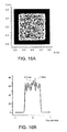
Figs. 6A through 6C are diagrams showing a calculation result representing the light intensity of the excitation light in a plane perpendicular to a principal ray of the excitation light. -
Fig. 7 is a schematic explanatory diagram of a polarization conversion element. -
Fig. 8 is an explanatory diagram showing a modified example of the light source device according to the first embodiment. -
Figs. 9A through 9C are diagrams showing a calculation result representing the light intensity of the excitation light in a plane perpendicular to a principal ray of the excitation light. -
Fig. 10 is an explanatory diagram showing a modified example of the light source device according to the first embodiment. -
Figs. 11A through 11C are explanatory diagrams showing a modified example of the light source device according to the first embodiment. -
Fig. 12 is an explanatory diagram showing a modified example of the light source device according to the first embodiment. -
Fig. 13 is an explanatory diagram showing a modified example of the light source device according to the first embodiment. -
Fig. 14 is a schematic diagram showing a light source device according to a second embodiment of the invention. -
Figs. 15A and 15B are explanatory diagrams showing a behavior of excitation light having entered a lens integrator. -
Figs. 16A and 16B are diagrams showing a calculation result representing the light intensity of the excitation light in a plane perpendicular to a principal ray of the excitation light. - Hereinafter, a light source device and a projector according to a first embodiment of the invention will be explained with reference to
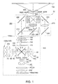
Figs. 1 through 13 . It should be noted that in all of the drawings described below, the sizes and the ratios between the sizes of the constituents are arbitrarily made different from each other in order for making the drawings eye-friendly. -
Fig. 1 is a schematic diagram showing thelight source device 100 and the projector PJ according to the present embodiment. As shown in the drawing, the projector PJ includes thelight source device 100, a color separationoptical system 200, a liquid crystal light valve (light modulation element) 400R, a liquid crystallight valve 400G, a liquid crystallight valve 400B, acolor combining element 500, and a projectionoptical system 600. - The projector PJ generally operates as follows. The light emitted from the
light source device 100 is separated by the color separationoptical system 200 into a plurality of colored lights. The plurality of colored lights thus separated into by the color separationoptical system 200 enters and is then modulated by the corresponding liquid crystallight valves light valves color combining element 500. The light thus combined by thecolor combining element 500 is projected by the projectionoptical system 600 on atarget projection surface 700 such as a wall or a screen in an enlarged manner, and thus a full-color projection image is displayed. - Hereinafter, each of the constituents of the projector PJ will be explained.
- The
light source device 100 has twolight sources 10B (a first light source 10Ba, a second light source 10Bb) for emitting the blue light. - The
light source device 100 has a configuration in which the light source 10Ba, a collimatingoptical system 20, alens integrator 30, a light wavelength selectingoptical system 40, an overlappingoptical system 50, alight emitting element 60,lens array 120,lens array 130, apolarization conversion element 140, and an overlappinglens 150 are disposed in this order when viewed along the light path of the light emitted from the light source 10Ba. - Here, the light source 10Ba and the collimating
optical system 20 constitute a light source section in the embodiment of the invention. Further, asecond lens array 34 and the overlappingoptical system 50 constitute a light collection optical system in the embodiment of the invention. Here, thesecond lens array 34 is included in thelens integrator 30. - Further, the
light source device 100 has a configuration in which the light source 10Bb, acollimator lens array 22b, a collectinglens 70, adiffuser 80, a collimatinglens 90, the light wavelength selectingoptical system 40, thelens array 120,lens array 130, thepolarization conversion element 140, and the overlappinglens 150 are disposed in this order when viewed along the light path of the light emitted from the light source 10Bb. - In the
light source device 100 having such a configuration, the blue light emitted from the light source 10Ba is applied to thelight emitting element 60, and is used as the excitation light for making the fluorescence be emitted from the fluorescent body provided to thelight emitting element 60. The fluorescence emitted from thelight emitting element 60 is mixed with the blue light emitted from the light source 10Bb on the light path, and is then emitted from thelight source device 100 as a white light L used as the illumination light for the liquid crystal light valves. - Hereinafter, each of the constituents will be explained first while explaining the behavior of the light emitted from the first light source 10Ba, and then each of the constituents will be explained while explaining the behavior of the light emitted from the second light source 10Bb.
-
Fig. 2 is a front view of the light source 10Ba. As shown in the drawing, the light source 10Ba is a laser source array having laser sources (solid-state light sources) 12 arranged in a 5x5 two-dimensional array (25 in total) so as to form a square shape on asubstrate 11. The laser sources 12 each have a rounded rectangular planar shape, and are arranged so that the long axis directions thereof are the same. - The light source 10Ba emits a blue (having a peak emission intensity at about 445nm; see
Fig. 3A ) laser beam as the excitation light for exciting the fluorescent material provided to thelight emitting element 60. What is denoted with the symbol B inFig. 3A is a colored light component emitted by the light source 10Ba as the excitation light. It should be noted that it is also possible to assume that just one laser source is used instead of the laser source array shown inFig. 2 . Further, the light source for emitting the colored light having a peak wavelength other than 445nm can also be adopted providing the light has the wavelength capable of exciting the fluorescent material described later. InFig. 1 , the excitation light emitted from the light source 10Ba is denoted by the reference symbol B. -
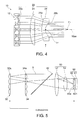
Fig. 4 is a side view of the light source 10Ba. As shown in the drawing, the excitation light emitted from the light source 10Ba is collimated by a firstcollimator lens array 22a included in the collimatingoptical system 20. Subsequently, the light beam of the excitation light collected by a collectinglens 24 proceeds toward a focal point F1 of the collectinglens 24, and is then collimated again by a collimatinglens 26. By being transmitted through such a collimatingoptical system 20, the excitation light is narrowed in the total width of the bundle of the light beams. - Here, the collimating
lens 26 has anentrance surface 26a formed as a convex surface having a spherical shape and anexit surface 26b formed as a concave surface having an aspherical shape. In further specific explanation of the shape of theexit surface 26b, the aspherical shape of theexit surface 26b of the collimatinglens 26 is arranged to be a shape approximately fulfilling the relationship expressed by Formula (2). Specifically, in theexit surface 26b, it is arranged that the light with a high degree of parallelization can be emitted by adopting a shape of a quadric surface of revolution as the aspherical shape of theexit surface 26b.
- Here, "r" and "Z" are coordinate values in the rθZ cylindrical coordinate system taking the intersecting point between the
exit surface 26b of the collimatinglens 26 and the center axis 10ax of the bundle of the light beams of the excitation light as the origin L0, and axisymmetrical about the center axis 10ax as shown inFig. 4 . It should be noted that inFig. 4 the Z direction takes the emission direction of the excitation light as the positive direction. The symbol "r" represents the distance from the origin L0 in the direction perpendicular to the center axis 10ax. The symbol "θ" represents the angle with the predetermined r direction, but the aspherical shape does not depend on the angle θ as is understood from Formula (2). - Further, in Formula (2), the paraxial curvature c represents the curvature of a spherical shape in the case of assuming that the light beam of the excitation light collected by the collecting
lens 24 is converted into a parallel beam of light using a plano-concave lens having the spherical shape. In other words, it results that in the paraxial area (the area adjacent to the rotational axis), the light beam of the excitation light collected by the collectinglens 24 can be converted into a parallel beam of light by using the plano-concave lens having the curvature c. - The symbol "K" is a value called a conic constant. The shape of the quadric surface of revolution is limited to a specific shape depending on the value of the conic constant K. Specifically, if the value of the conic constant K fulfills -1 <K<0, the aspherical surface becomes an ellipsoid of revolution. Further, if the value of the conic constant K fulfills K=-1, the aspherical surface becomes a paraboloid of revolution. Still further, if the value of the conic constant K fulfills K<-1, the aspherical surface becomes a hyperboloid of revolution.
- Further, the third term of the left-hand side is a function called a general aspheric term and depending on the distance r, but is a sufficiently small value, and is therefore disregarded in the present embodiment.
- The shape of the quadric surface of revolution of the aspherical surface of the collimating
lens 26 in the present embodiment is determined by the following method based on Formula (3) below in which the third term of the left-hand side in Formula (2) is disregarded.
- Firstly, the value of the paraxial curvature c is obtained in consideration of the shape of the collecting
lens 24, the curvature of theentrance surface 26a of the collimatinglens 26, the refractive index n of the collimatinglens 26, the thickness of the central part of the collimatinglens 26, and the installation location of the collimatinglens 26. - Specifically, the shape of the collecting
lens 24, and the curvature of theentrance surface 26a, the refractive index n, the thickness of the central part, and the installation location of the collimatinglens 26 are firstly determined in advance. Further, a concave lens having the curvature of the entrance surface, the refractive index, and the thickness of the central part identical thereto, and at the same time having the spherical exit surface is assumed as an alternative of the collimatinglens 26. Then, the curvature of the exit surface of the concave lens is obtained, with which the transmitted light can be converted into parallel light in the paraxial area (the area adjacent to the rotational axis) in the case in which the concave lens described above is disposed at the installation location of the collimatinglens 26 with respect to the collecting lens having the shape identical to the shape determined in advance. - The value of the curvature thus obtained is the paraxial curvature c in Formula (3) defining the shape of the
exit surface 26b. Here, if theentrance surface 26a of the collimatinglens 26 is set to a plane surface, the curvature of theentrance surface 26a is set to 0. - Then, the conic constant K is obtained. In the
light source device 100 of the present embodiment, the conic constant K is set to a condition with which the parallel light is emitted by performing a simulation repeatedly using Formula (3) while varying the value thereof. In this simulation, it is possible to take the case, in which the diameter of a light spot at a focal point becomes the smallest when a bundle of the light beams emitted from thelight source device 100 is collected by an ideal lens without aberration, as the condition of emitting the approximately parallel light. - By using the
collimating lens 26 designed in such a manner as described above, it is possible to make the excitation light transmitted through the collimatingoptical system 20 to be the light with a high degree of parallelization. - The excitation light transmitted through the collimating
optical system 20 enters thelens integrator 30. Thelens integrator 30 has afirst lens array 32 and thesecond lens array 34, these lens arrays are arranged on the light path in this order. Thefirst lens array 32 and thesecond lens array 34 are for homogenizing the brightness distribution of the light emitted from the collimatingoptical system 20. - The excitation light transmitted through the
lens integrator 30 enters the light wavelength selectingoptical system 40. The light wavelength selectingoptical system 40 has adichroic mirror 42 and adichroic mirror 44. The dichroic mirrors 42, 44 are each formed by, for example, stacking a dielectric multilayer film on a glass surface. - The dichroic mirrors 42, 44 have the wavelength selectivity of selectively reflecting the colored light in the wavelength band of the excitation light, and transmitting the colored light in the other wavelength band. Specifically, the
dichroic mirror 42 reflects the blue light, and transmits the light (e.g., the light with the wavelength longer than 480nm) with the wavelength longer than the blue light. On the other hand, thedichroic mirror 44 transmits the blue light, and reflects the light (e.g., the light with the wavelength longer than 480nm) with the wavelength longer than the blue light. Here, the excitation light is transmitted through thedichroic mirror 44, and at the same time reflected by thedichroic mirror 42. - The excitation light reflected by the
dichroic mirror 42 enters the overlappingoptical system 50, and is then imaged on thelight emitting element 60. -
Fig. 5 illustrates the behavior of the excitation light until the excitation light (the blue light B) having entered thelens integrator 30 is applied to thelight emitting element 60. - As shown in
Fig. 5 , thefirst lens array 32 includes a plurality of firstsmall lenses 32a, and thesecond lens array 34 includes a plurality of secondsmall lenses 34a. Further, the planar shape of the firstsmall lens 32a and the planar shape of the secondsmall lens 34a are arranged to be roughly similar to the planar shape of alight irradiation surface 60a of thelight emitting element 60. - In the
first lens array 32 and thesecond lens array 34, one of the firstsmall lenses 32a and one of the secondsmall lenses 34a correspond to each other in a one-to-one manner. The light emitted from the collimatingoptical system 20 enters the plurality of firstsmall lenses 32a while being spatially separated, and each of the firstsmall lenses 32a images the incident light on a corresponding one of the secondsmall lenses 34a. Thus, the secondary light source image is formed in each of the secondsmall lenses 34a. - Further, the light emitted from each of the second
small lenses 34a is collected by the overlappingoptical system 50 configured including afirst lens 52 and asecond lens 54 via thedichroic mirror 42, and is then imaged on thelight emitting element 60. In other words, the light collection optical system configured including thesecond lens array 34 and the overlappingoptical system 50 images the incident light on thelight irradiation surface 60a of the correspondinglight emitting element 60. - As shown in
Fig. 5 , thelight emitting element 60 has a plate likesubstrate 61 and afluorescent layer 62 formed on the excitation light entrance side surface of thesubstrate 61. Thefluorescent layer 62 is formed to have, for example, a roughly square shape of 1mmx1mm in a plan view, and hasfluorescent particles 621 for emitting fluorescence. Such afluorescent layer 62 has a function of absorbing the excitation light (the blue light) and converting it into yellow (having the peak emission intensity at about 550nm; seeFig. 3B ) fluorescence. - The component indicated by the reference symbol R in
Fig. 3B is a colored light component available as the red light out of the yellow light emitted by thefluorescent layer 62, and the component indicated by the reference symbol G is a colored light component available as the green light similarly. InFig. 1 , the red light is denoted by the reference symbol R, the green light is denoted by the reference symbol G, and the fluorescence including the red light R and the green light G is denoted by the reference symbol RG. - In such a configuration, the optical system configured including the
second lens array 34 and the overlappingoptical system 50 is preferably configured so that the lens plane of thefirst lens array 32 and thelight irradiation surface 60a of thelight emitting element 60 are in a conjugate relationship. Specifically, it is preferable that it is configured so that the object plane of the optical system configured including thesecond lens array 34 and the overlappingoptical system 50 coincide with the lens plane of thefirst lens array 32, and the image plane thereof coincide with thelight irradiation surface 60a of thelight emitting element 60. Thus, it results that thelight irradiation surface 60a is irradiated with the excitation light having the homogenized intensity distribution. - Here, "the lens plane of the
first lens array 32" denotes an imaginary plane connecting the valleys between the firstsmall lenses 32a provided to thefirst lens array 32. -
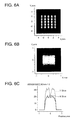
Figs. 6A through 6C show the calculation result representing the light intensity of the excitation light on a plane perpendicular to the principal ray of the excitation light, whereinFig. 6A is a distribution chart showing the light intensity of the excitation light entering thefirst lens array 32, andFig. 6B is a distribution chart showing the light intensity of the excitation light entering thelight irradiation surface 60a. InFigs. 6A and 6B , it is arranged that the higher the light intensity of the place is, the brighter the place is, and the lower the light intensity of the place is, the darker the place is to thereby display the light intensity in correspondence with the luminance of the area. - Further,
Fig. 6C is a graph showing the light intensity in the area passing through the origin and along the x axis and the y axis in the distribution chart ofFig. 6B . The horizontal axis ofFig. 6C represents the location (the coordinate) on the x axis or the y axis in the area shown inFig. 6B , and the vertical axis thereof represents the light intensity (the irradiance). - As shown in
Fig. 6A , in the spatial position before entering thefirst lens array 32, bright sections and dark sections exist discretely in the light intensity distribution of the excitation light in accordance with the light source 10Ba shown inFig. 2 . In contrast, as shown inFig. 6B , in the spatial position before entering thelight irradiation surface 60a, the excitation light is formed to have an approximately square shape of 1mmx1mm, and has a continuous light intensity distribution approximating the light intensity distribution of a so-called top hat profile in which the light intensity is roughly uniform throughout the entire area of thelight irradiation surface 60a as shown inFig. 6C . - The
light emitting element 60 is irradiated with the excitation light having the light intensity distribution approximating the homogenized distribution compared to that of the excitation light before being transmitted through thelens integrator 30 as described above. Further, the excitation light applied thereto is formed to have a shape roughly the same as the planar shape of thelight emitting element 60. Therefore, it becomes easy to irradiate the entire area of thelight irradiation surface 60a of thelight emitting element 60 so as not to cause the light saturation inside the surface thereof. Therefore, thelight emitting element 60 can be used as the secondary light source for preferably emitting the fluorescence RG from the entire area of thelight irradiation surface 60a. - The overlapping
optical system 50 functions as a pickup optical system with respect to the fluorescence RG emitted from thelight emitting element 60. Therefore, the fluorescence RG enters the light wavelength selectingoptical system 40 after being collimated by the overlappingoptical system 50. In the light wavelength selectingoptical system 40, the fluorescence RG is transmitted by thedichroic mirror 42, reflected by thedichroic mirror 44, and then emitted toward thelens array 120. - Then, each of the constituents will be explained while explaining the light emitted from the second light source 10Bb.
- The light source 10Bb has substantially the same configuration as that of the light source 10Ba shown in
Fig. 2 , and is formed of a laser source array for emitting the blue light. The blue light emitted from the light source 10Bb is collimated by the secondcollimator lens array 22b, and is then collected by the collectinglens 70. - The
diffuser 80 is disposed at the focal position of the collectinglens 70. Thediffuser 80 has a function of scattering the light transmitted therethrough. The blue light, which is coherent light, emitted from the light source 10Bb is scattered by thediffuser 80 to thereby provide a light path difference in the blue light, and thus the coherency is lowered. Therefore, it becomes difficult to cause the interference pattern called speckle when projected on thetarget projection surface 700. - The blue light transmitted through the
diffuser 80 enters and is then collimated by the collimatinglens 90, then enters the light wavelength selectingoptical system 40, and is then reflected by thedichroic mirror 42 to thereby be emitted toward thelens array 120. Therefore, the light emitted from the light wavelength selectingoptical system 40 becomes the white light L obtained by mixing the fluorescence RG including the red light and the green light mixed with each other and emitted from thelight emitting element 60, and the blue light B emitted from the light source 10Bb. - It should be noted that although it is assumed in the present embodiment that the light source 10Bb is the laser source array, the light source 10Bb is not required to be the laser source array providing the light source 10Bb can emit the blue light used for display.
- The
lens arrays optical system 40. Thelens array 120 includes a plurality of firstsmall lenses 122, and thelens array 130 includes a plurality of secondsmall lenses 132. In thelens array 120 and thelens array 130, the firstsmall lenses 122 and the secondsmall lenses 132 correspond to each other in a one-to-one manner. The light L emitted from the light wavelength selectingoptical system 40 enters the plurality of firstsmall lenses 122 while being spatially separated, and each of the firstsmall lenses 122 images the incident light on a corresponding one of the secondsmall lenses 132. Thus, the secondary light source image is formed in each of the secondsmall lenses 132. It should be noted that the outer shape of the firstsmall lenses 122 and the secondsmall lenses 132 is arranged to be roughly similar to the outer shape of the image forming areas of the respective liquid crystallight valves - The
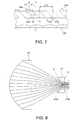
polarization conversion element 140 is for aligning the polarization state of the light L emitted from thelens arrays Fig. 7 , thepolarization conversion element 140 includes a plurality ofpolarization conversion cells 141. Thepolarization conversion cells 141 correspond to the secondsmall lenses 132 in a one-to-one manner. The light L from the secondary light source image formed on each of the secondsmall lenses 132 enters anentrance area 142 of a corresponding one of thepolarization conversion cells 141. - Each of the
polarization conversion cells 141 is provided with a polarization beam splitter film 143 (hereinafter referred to as a PBS film 143) and aretardation plate 145 so as to correspond to theentrance area 142. The light L having entered theentrance area 142 is split by thePBS film 143 into P-polarized light L1 and S-polarized light L2 with respect to thePBS film 143. One (here the S-polarized light L2) of the P-polarized light L1 and the S-polarized light L2 is reflected by a reflectingmember 144, and then enters theretardation plate 145. The S-polarized light L2 having entered theretardation plate 145 is converted in the polarization state into the polarization state of the other polarized light (here the P-polarized light L1) by theretardation plate 145 to thereby become P-polarized light L3, and is then emitted together with the P-polarized light L1. - The overlapping
lens 150 is for making the lights emitted from thepolarization conversion element 140 overlap with each other in the illuminated area. The light emitted from thelight source device 100 is spatially divided and then overlapped to thereby be homogenized in the luminance distribution, and enhanced in the axisymmetric property around the light beam axis 100ax. - The color separation
optical system 200 includesdichroic mirrors field lenses relay lenses dichroic mirror 210 reflects the green light and the blue light, and thedichroic mirror 220 reflects the green light. - The light L emitted from the
light source device 100 enters thedichroic mirror 210. The red light R out of the light L is incident on themirror 230 after passing through thedichroic mirror 210, and is then reflected by themirror 230, and further enters thefield lens 300R. The red light R is collimated by thefield lens 300R, and then enters the liquid crystallight valve 400R. - The green light G and the blue light B out of the light L are reflected by the
dichroic mirror 210, and are then incident on thedichroic mirror 220. The green light G is reflected by thedichroic mirror 220, and then enters thefield lens 300G. The green light G is collimated by thefield lens 300G, and then enters the liquid crystallight valve 400G. - The blue light B having passed through the
dichroic mirror 220 passes through therelay lens 260 and is then reflected by themirror 240, and then further passes through therelay lens 270 and is then reflected by themirror 250 to thereby enter thefield lens 300B. The blue light B is collimated by thefield lens 300B, and then enters the liquid crystallight valve 400B. - The liquid crystal
light valves light valves light valves color combining element 500. - The
color combining element 500 is formed of a dichroic prism or the like. The dichroic prism has a structure having four triangular prisms bonded to each other. The surfaces bonded to each other in the triangular prisms form the internal surfaces of the dichroic prism. A mirror surface for reflecting the red light R and transmitting the green light G and a mirror surface for reflecting the blue light B and transmitting the green light G are formed perpendicular to each other in the internal surfaces of the dichroic prism. The green light G having entered the dichroic prism passes through the mirror surfaces, and is emitted directly. The red light R and the blue light B having entered the dichroic prism are selectively reflected or transmitted on the mirror surfaces, and then emitted in the same direction as the emission direction of the green light G. In such a manner as described above, the three colored lights (images) are overlapped to thereby be combined with each other, and the colored light thus combined is projected by the projectionoptical system 600 on thetarget projection surface 700 in an enlarged manner. - In the projector PJ according to the present embodiment, the image display is performed in such a manner as described above.
- According to the
light source device 100 having such a configuration as described above, since the light saturation phenomenon is prevented from occurring in thelight emitting element 60, the light intensity is stabilized, and the light source with higher luminance efficiency compared to the related art can be obtained. - Further, according to the projector PJ having such a configuration as described above, since the light saturation phenomenon is prevented from occurring, the light intensity of the light emitted from the light source device is stabilized, and the variation in brightness is suppressed to thereby make it possible to perform high-quality image display.
- It should be noted that although it is assumed in the present embodiment that the
exit surface 26b has the aspherical shape in thecollimating lens 26, it is also possible to assume that the lens having the entrance surface shaped like an aspherical surface is used. - A collimating
lens 27 shown inFig. 8 is a plano-convex lens having anentrance surface 27a formed to have the quadric surface of revolution fulfilling the relationship of Formula (3), and anexit surface 27b formed as a plane surface. By using such acollimating lens 27, an advantage that the light beam is highly parallelized can easily be obtained compared to the case of using thecollimating lens 26 described above. - Specifically, the bundle of the light beams emitted from the collimating
lens 26 described above is changed in the proceeding direction twice due to the refraction in theentrance surface 26a and the refraction in theexit surface 26b of the collimatinglens 26, and is then emitted therefrom. On the other hand, the bundle of the light beams emitted from the collimatinglens 27 is collimated by the refraction on theentrance surface 27a of the collimatinglens 27, and is therefore changed in the proceeding direction only once, and then emitted. Therefore, it is difficult for the disturbance in parallelization due to the molding error of the lens to occur. Therefore, by using thecollimating lens 27, it becomes possible to obtain the light beam with a higher degree of parallelization. - On the other hand, the bundle of the light beams emitted from the collimating
lens 27 described above has the light intensity distribution shown inFigs. 9A through 9C. Figs. 9A through 9C show the calculation result representing the light intensity of the excitation light in a plane perpendicular to the principal ray of the excitation light in the case of using thecollimating lens 27, and correspond toFigs. 6A through 6C , respectively. - As shown in
Fig. 9A , if thecollimating lens 27 is used, the light intensity distribution of the excitation light is discretely disposed, and the pincushion distortion is caused therein at the spatial position before entering thefirst lens array 32. This is because in thecollimating lens 27 a substantial difference in the incident angle of the incident light beam is caused between the center (reference symbol α) and the periphery (reference symbol β) of the collimatinglens 27 as shown inFig. 8 , and therefore, the intensity distribution in which the intensity is high in the central part and low in the periphery is apt to occur in the bundle of the light beams emitted from the collimatinglens 27. - Further, as shown in
Figs. 9B and 9C , at the spatial position before entering thelight irradiation surface 60a, the excitation light has the light intensity distribution less homogeneous than the light intensity distribution shown inFigs. 6B and 6C although approximating the light intensity distribution shaped like a top hat homogenous in the area having the roughly square shape of 1mmx1mm. That may be attributed to the consequence of reflecting the unevenness (seeFig. 9A ) of the light intensity before entering thefirst lens array 32. - The quadric surface of revolution of the aspherical surface of such a
collimating lens 27 is determined by the following process based on Formula (3). - Specifically, the shape of the collecting
lens 24, and the refractive index n, the thickness of the central part, and the installation location of the collimatinglens 27 are firstly determined in advance. Further, a concave lens having the curvature of the entrance surface, the refractive index, and the thickness of the central part identical thereto, and at the same time having the spherical exit surface is assumed as an alternative of the collimatinglens 27. Then, the curvature of the entrance surface of the concave lens is obtained, with which the conversion into parallel light is possible if no spherical aberration exists in the case in which the concave lens described above is disposed at the installation location of the collimatinglens 27 with respect to the collecting lens having the shape identical to the shape determined in advance. The value of the curvature obtained in such a manner is used as the paraxial curvature c. - Then, the conic constant K is obtained. Here, in the
collimating lens 27, theentrance surface 27a has the aspherical shape set based on Formula (3), and therefore, the excitation light entering thecollimating lens 27 is changed in the proceeding direction to the roughly parallel direction due to the refraction on theentrance surface 27a, and is hardly subjected to the refraction on theexit surface 27b. As a result, the relationship between the refractive index n and the conic constant K of the collimatinglens 27 becomes constant. It should be noted that the conic constant K of the aspherical surface of the reflecting surface the collimatinglens 27 is roughly determined by K=-n2. - Therefore, in the present modified example, the conic constant K can be obtained by K=-n2, and there is no need to perform the simulation required in the case of using the
collimating lens 26. The conic constant K of the aspherical surface of such acollimating lens 27 is in a range of -2.1>K>-3.8. Therefore, in the case of adopting the aspherical shape as theentrance surface 27a, it is preferable to adopt a hyperboloid of revolution as theentrance surface 27a. - Further, although in the present embodiment it is assumed that the light source 10Ba shown in
Fig. 2 is used as the light source of the excitation light, it is also possible to use the light source section shown inFigs. 10 and11A through 11C described below. -
Fig. 10 is a schematic diagram showing alight source device 101. In thelight source device 101, alight source 13 is used as the light source for emitting the excitation light instead of the light source 10Ba described above. There is adopted a configuration in which the blue light B emitted from thelight source 13 is collimated by acollimator lens array 28, and is then reflected by a reflectingsection 29 including a plurality of reflectingmirrors 29a to thereby enter the collectinglens 24. - The reflecting
mirrors 29a are disposed so as to correspond to the blue lights B emitted from therespective laser sources 12, and have a function of changing the pitch of the principal rays from W1 to W2 (W1>W2). The reflectingmirrors 29a are disposed at a distance of W3, and have a configuration of reflecting the lights by the respective reflectingmirrors 29a to thereby change the pitch of the principal rays. -
Fig. 11A is a plan view of thelight source 13 provided to thelight source device 101. As shown inFig. 11A , thelight source 13 is a laser source array havinglaser sources 12 arranged in a 10x5 two-dimensional array (50 in total) so as to form a rectangular shape on asubstrate 11. The laser sources 12 each have a rectangular planar shape, and are arranged so that the long axis directions thereof are the same. Further, thelaser sources 12 are arranged in the short axis direction at the pitch W1. - In such a
light source 13, the laser beams (the blue lights B) emitted from therespective laser sources 12 come to have the pitch of the principal rays corresponding to the arrangement pitch W1 of thelaser sources 12 as shown inFig. 11B . - Therefore, as shown in
Fig. 11C , the laser beams (the blue lights B) reflected by the reflectingsections 29 come to have the pitch W2 of the principal rays, and the light intensity of the whole of the bundle of the light beams increases. - In the
light source device 101 having such a configuration, since the density of the light emitted from thelight source 13 can be increased, there can be obtained the light source device capable of increasing the light intensity of the light applied to thelight emitting element 60 to thereby emit the high-intensity fluorescence. - Further, although in the present embodiment it is assumed that the red light R and the green light G are included in the fluorescence RG emitted by the
light emitting element 60, this is not a limitation. It is also possible to assume that the fluorescence including the green light G alone is emitted as in the case of, for example, alight emitting element 63 of alight source device 102 shown inFig. 12 . - On this occasion, it is preferable that a
light source 10R for emitting the red light is prepared besides the light source 10Bb for emitting the blue light used for the display as shown inFig. 12 . Specifically, it is preferable to adopt the configuration of disposing adichroic mirror 46 for reflecting the blue light and transmitting the other light on both of the light paths of the blue light B emitted from the light source 10Bb and the red light R emitted from thelight source 10R to thereby mix the blue light and the red light on the light paths, and then guiding the light thus mixed to the collectinglens 70. Thelight source 10R can be a laser source array or have a different configuration providing thelight source 10R can emit the red light. - Further, although in the present embodiment there is adopted the
light emitting element 60 having the reflective configuration of emitting the fluorescence to the side where the excitation light enters, it is also possible to assume that there is adopted the transmissive configuration of emitting the fluorescence to the surface opposed to the surface where the excitation light enters. -
Fig. 13 is a schematic diagram of alight source device 103 having a transmissivelight emitting element 64. - As shown in the drawing, in the
light source device 103, the excitation light (the blue light B) emitted from thelight source 10B enters one (anentrance surface 64a) of the surfaces of thelight emitting element 64 via the collimatingoptical system 20, thelens integrator 30, and the overlappingoptical system 50. In thelight emitting element 64, a part of the excitation light is absorbed, and is then converted into the fluorescence RG including the red light and the green light, and the rest of the excitation light is transmitted therethrough without being absorbed. Therefore, the white light L obtained by mixing the excitation light (the blue light B) not absorbed and the fluorescence RG is emitted from the other (anexit surface 64b) of the surfaces of thelight emitting element 64. - The light L emitted from the
light emitting element 64 is prevented from spreading by a pickupoptical system 59 including first andsecond pickup lenses lens arrays polarization conversion element 140, and the overlappinglens 150. - Since the light intensity of the excitation light emitted from the
light source 10B is averaged by thelens integrator 30, and then the excitation light is made to enter the fluorescent layer provided to thelight emitting element 64, even such alight source device 103 can be made to have high luminance efficiency. - Further, although in the present embodiment, the collecting
lens 24 and thecollimating lens 26 included in the collimatingoptical system 20 form an afocal optical system of a so-called Galileo type, it is also possible to assume that a convex lens is used instead of the collimatinglens 26 to thereby form an afocal optical system of a so-called Kepler type. - Further, although in the present embodiment it is assumed that the lens plane of the
first lens array 32 and thelight irradiation surface 60a of thelight emitting element 60 are in a conjugate relationship via the light collection optical system, the advantage obtained by overlapping the excitation light via thefirst lens array 32 can be expected even if the excitation light is not imaged on thelight irradiation surface 60a, and the light intensity of the excitation light tends to be averaged. Therefore, it is possible to prevent the light saturation phenomenon in thelight emitting element 60 to thereby obtain a light source with high luminance efficiency. - Further, although in the present embodiment it is assumed that the excitation light thus collected is formed to have a roughly square shape with the irradiation area of 1mmx1mm, and the size thereof is roughly equal to the planar area of the
fluorescent layer 62, even if it is assumed, for example, that the irradiation area of the excitation light is slightly larger than thefluorescent layer 62, the light saturation in thelight emitting element 60 can be prevented, and therefore, the improvement in the luminance efficiency can be expected. - Further, in the present embodiment, it is arranged that the planar shape of a small lens of the first and
second lens arrays light irradiation surface 60a are roughly similar to each other. However, although a part of the excitation light is wasted if they are not similar to each other, improvement in the luminance efficiency is expected since the light saturation in thelight emitting element 60 is prevented. - Further, although it is assumed in the present embodiment that the concave surface of the collimating
lens 26 is designed using Formula (3) described above, it is also possible to use other generally known design methods of the aspherical surface. -
Fig. 14 is an explanatory diagram of a light source device according to a second embodiment of the invention. In the following explanation, the constituents common to the present embodiment and the first embodiment are denoted by the same reference symbols, and the detailed explanation therefor will be omitted. - As shown in
Fig. 14 , a configuration of alight source device 104 is partially common to thelight source device 100 according to the first embodiment. The difference is that thelens integrator 30 is not formed of a pair of lens arrays, and thefirst lens array 32 is used alone. In the present embodiment, the overlappingoptical system 50 functions as the light collection optical system of the embodiment of the invention. -
Figs. 15A and 15B are explanatory diagrams showing the function of thefirst lens array 32 and the overlappingoptical system 50. InFigs. 15A and 15B , the overlappingoptical system 50 is schematically illustrated as a single convex lens for the sake of simplification. It is assumed that the overlappingoptical system 50 has no spherical aberration, or the spherical aberration thereof is reduced by correction. - As shown in
Fig. 15A , in the optical system configured including thefirst lens array 32 and the overlappingoptical system 50, there is adopted a configuration in which the excitation light (the blue light B) entering thefirst lens array 32 is parallelized, and the principal rays of the excitation lights transmitted through thefirst lens array 32 and the overlappingoptical system 50 pass through a focal point F2 of the overlappingoptical system 50. In other words, in the optical system having thefirst lens array 32 in one end of the optical system and the overlappingoptical system 50 in the other end of the optical system, the object plane is set to infinity. In other words, it is arranged that the optical system configured including thefirst lens array 32 and the overlappingoptical system 50 is object-side telecentric. In such an optical system, the incident excitation light (the blue light B) enters the overlappingoptical system 50 after being transmitted through thefirst lens array 32, and the excitation light emitted from the overlappingoptical system 50 passes through an exit pupil P with a certain width related to the overlappingoptical system 50. - In such a configuration, the width of the exit pupil P is determined to be a certain size in accordance with the numerical aperture NA and the focal distance Lb of the overlapping
optical system 50. Further, the shape of the exit pupil P becomes similar to thesmall lens 32a constituting thefirst lens array 32. In other words, the width of the exit pupil P is always constant independently of the distance La between the overlappingoptical system 50 and thefirst lens array 32. For example, the exit pupil P is designed to have a roughly square shape of 1mmx1mm. - Therefore, as shown in
Fig. 15B , by disposing thelight emitting element 60 having the same size as the exit pupil at the position of the focal point F2 of the overlappingoptical system 50, and setting the plane conjugate to thelight irradiation surface 60a to infinity, it becomes possible to reduce (eliminate the second lens array shown inFig. 1 ) the number of lens arrays used compared to the case of thelight source device 100 of the first embodiment. As a result, it is possible to average the light intensity of the excitation light with a small number of components, and irradiate thelight emitting element 60 with the excitation light. -
Figs. 16A and 16B show the calculation result representing the light intensity of the excitation light in a plane perpendicular to the principal ray of the excitation light in thelight source device 104, and correspond toFigs. 6B and 6C , respectively. - As shown in
Fig. 16B , in the spatial position before entering thelight emitting element 60, the excitation light is formed to have an approximately square shape of 1mmx1mm, and has a continuous light intensity distribution approximating the light intensity distribution of a so-called top hat profile in which the light intensity is roughly uniform throughout the entire area as shown inFig. 16C . - In the
light source device 104, since the excitation light divided by thefirst lens array 32 into a plurality of light beams is collected by the overlappingoptical system 50, the light intensity distribution is averaged. In addition, since the excitation light is not imaged in the exit pupil P shown inFig. 15A , the image of the excitation light blurs, and the light intensity is easily averaged. Therefore, it becomes possible to preferably average the light intensity distribution even in the discrete light source such as the light source 10Ba. - According to the
light source device 104 having such a configuration as described above, since the light saturation phenomenon is prevented from occurring, the light intensity is stabilized, and the light source with higher luminance efficiency compared to the related art can be obtained. - It should be noted that although in the present embodiment the explanation is presented assuming that the collimating
lens 26 is used, it is also possible to assume that the collimatinglens 27 shown inFig. 8 is used. The collimatinglens 27 having a concave entrance surface and a flat exit surface is capable of further enhancing the degree of parallelization of the excitation light transmitted through the collimatinglens 27 than in the case of the collimatinglens 26. Therefore, it becomes easier to perform averaging of the excitation light using thefirst lens array 32 and the overlapping optical system 50 (the light collection optical system). - Further, in the present embodiment, it is assumed that the planar area of the
light irradiation surface 60a of thelight emitting element 60 is roughly equal to the size of the exit pupil P. However, even in the case, for example, in which the exit pupil P is larger, improvement in the luminance efficiency is expected since the light saturation in thelight emitting element 60 is prevented although a part of the excitation light is wasted. - Further, although it is assumed in the present embodiment that the
light irradiation surface 60a is disposed so as to overlap the focal point F2 of the overlapping optical system 50 (the light collection optical system), even if thelight irradiation surface 60a is displaced from the focal point F2, the advantage obtained by overlapping the excitation light via thefirst lens array 32 can be expected, and the light intensity of the excitation light tends to be averaged. Therefore, it is possible to prevent the light saturation phenomenon in thelight emitting element 60 to thereby obtain a light source with high luminance efficiency. - Although the explanation is hereinabove presented regarding the preferable embodiments of the invention with reference to the accompanying drawings, the invention is not limited to the embodiments described above. The various shapes and combinations of the constituents presented in the embodiments described above are provided for exemplification only, and can be modified in various ways within the scope of the invention in accordance with design needs and so on.
Claims (6)
- A light source device (100) comprising:a light source section including a plurality of solid-state light sources (10B) adapted to emit excitation light, and adapted to emit the excitation light as a parallel beam of light;a lens array (32) adapted to divide the excitation light into a plurality of partial light beams;a light collection optical system (50) adapted to collect the excitation light divided into the plurality of partial light beams; anda light emitting element (60) adapted to emit fluorescence by being excited by the excitation light collected by the light collection optical system;wherein the light collection optical system includes:a second lens array (34) which the plurality of partial light beams enter, the second lens array forming a pair together with the lens array (32), and which the partial light beams enter, andan overlapping optical system (50) adapted to make the plurality of partial light beams emitted from the second lens array overlap with each other on the light emitting element, andwherein a lens plane of the lens array (32) and a light irradiation surface (60a) of the light emitting element (60) are in a conjugate relationship via the light collection optical system.
- The light source device according to Claim 1, wherein
a planar shape of a small lens constituting the lens array (32) is similar to a planar shape of the light irradiation surface, and
a planar area of the light irradiation surface (60) and an irradiation area of the excitation light illuminating a plane parallel to the light irradiation surface at a same spatial position as the light irradiation surface are substantially equal to each other. - The light source device according to Claim 1, wherein
the light source section includes
a collecting lens adapted to collect the excitation light emitted from the plurality of solid-state light sources, and
a collimating lens adapted to collimate the excitation light emitted from the collecting lens, and
the collimating lens has a concave surface having a shape of a quadric surface of revolution in either one of an entrance surface and an exit surface. - The light source device according to Claim 3, wherein
the collimating lens has a spherical convex surface as the entrance surface, and the concave surface as the exit surface. - The light source device according to Claim 3, wherein
assuming that coordinate values in an rθZ cylindrical coordinate system taking an intersecting point between the concave surface and a center axis of the parallel beam of light as an origin, the center axis as a Z axis, and an axis perpendicular to the center axis as an r axis are r and Z, a paraxial curvature is c, and a conic constant is K,
the concave surface has a shape represented by Formula (1):
- A projector comprising:the light source device according to any one of the preceding claims;a light modulation element (400) adapted to modulate light emitted from the light source device; anda projection optical system (600) adapted to project the light modulated by the light modulation element.
Applications Claiming Priority (1)
| Application Number | Priority Date | Filing Date | Title |
|---|---|---|---|
| JP2010265165A JP5699568B2 (en) | 2010-11-29 | 2010-11-29 | Light source device, projector |
Publications (2)
| Publication Number | Publication Date |
|---|---|
| EP2458437A1 EP2458437A1 (en) | 2012-05-30 |
| EP2458437B1 true EP2458437B1 (en) | 2013-12-18 |
Family
ID=45217206
Family Applications (1)
| Application Number | Title | Priority Date | Filing Date |
|---|---|---|---|
| EP11189055.4A Active EP2458437B1 (en) | 2010-11-29 | 2011-11-14 | Light source device and projector |
Country Status (6)
| Country | Link |
|---|---|
| US (1) | US9810977B2 (en) |
| EP (1) | EP2458437B1 (en) |
| JP (1) | JP5699568B2 (en) |
| KR (1) | KR101297890B1 (en) |
| CN (1) | CN102478754B (en) |
| TW (1) | TWI446092B (en) |
Families Citing this family (65)
| Publication number | Priority date | Publication date | Assignee | Title |
|---|---|---|---|---|
| JP5673247B2 (en) * | 2011-03-15 | 2015-02-18 | セイコーエプソン株式会社 | Light source device and projector |
| JP5979416B2 (en) * | 2011-04-20 | 2016-08-24 | パナソニックIpマネジメント株式会社 | Light source device and image display device |
| JP5798430B2 (en) * | 2011-10-03 | 2015-10-21 | 浜松ホトニクス株式会社 | Fluorescence observation apparatus and fluorescence observation method |
| JP5589007B2 (en) * | 2012-01-18 | 2014-09-10 | シャープ株式会社 | Light emitting device, lighting device, and vehicle headlamp |
| JP6078976B2 (en) * | 2012-04-12 | 2017-02-15 | セイコーエプソン株式会社 | projector |
| JP6019891B2 (en) | 2012-07-30 | 2016-11-02 | セイコーエプソン株式会社 | Light source device and projector |
| DE112013004405B4 (en) * | 2012-09-10 | 2020-10-08 | Mitsubishi Electric Corporation | Light source device |
| JP6089616B2 (en) * | 2012-11-20 | 2017-03-08 | セイコーエプソン株式会社 | Light source device and projector |
| JP2014119471A (en) * | 2012-12-13 | 2014-06-30 | Seiko Epson Corp | Light source device and projector |
| TWI459122B (en) * | 2013-01-17 | 2014-11-01 | Delta Electronics Inc | Optical system |
| CN106647124A (en) * | 2013-02-04 | 2017-05-10 | 深圳市光峰光电技术有限公司 | Laser light source, wavelength conversion light source, light composition light source and projection display equipment |
| CN104020632B (en) * | 2013-02-28 | 2016-08-24 | 深圳市绎立锐光科技开发有限公司 | Light-emitting device and relevant projecting system |
| CN107632487B (en) * | 2013-04-20 | 2020-03-24 | 深圳光峰科技股份有限公司 | Light emitting device and related light source system |
| CN103279005B (en) * | 2013-05-13 | 2015-08-19 | 深圳市绎立锐光科技开发有限公司 | LASER Light Source, wavelength convert light source, conjunction radiant and optical projection system |
| WO2014196015A1 (en) * | 2013-06-04 | 2014-12-11 | Necディスプレイソリューションズ株式会社 | Illumination optical system and projector |
| CN105264437A (en) * | 2013-06-04 | 2016-01-20 | Nec显示器解决方案株式会社 | Illumination optical system and projector |
| US9740088B2 (en) * | 2013-06-07 | 2017-08-22 | Nec Display Solutions, Ltd. | Light source apparatus and projection display apparatus provided with same including waveplate and dichroic prism |
| JP6177596B2 (en) | 2013-06-18 | 2017-08-09 | シャープ株式会社 | Light emitting device |
| US9423680B2 (en) * | 2013-07-23 | 2016-08-23 | Seiko Epson Corporation | Light source apparatus that irradiates a phosphor layer with excitation light and projector |
| JP6299460B2 (en) * | 2013-10-16 | 2018-03-28 | セイコーエプソン株式会社 | projector |
| JP6270407B2 (en) | 2013-10-23 | 2018-01-31 | キヤノン株式会社 | Light source device and projection display device |
| JP2015153889A (en) * | 2014-02-14 | 2015-08-24 | 三菱電機株式会社 | laser combining optical device |
| JP6578631B2 (en) | 2014-07-09 | 2019-09-25 | セイコーエプソン株式会社 | Lighting device and projector |
| TWI534509B (en) | 2014-08-19 | 2016-05-21 | 台達電子工業股份有限公司 | Solid state illuminator and operating method using the same |
| JP6413498B2 (en) * | 2014-08-29 | 2018-10-31 | セイコーエプソン株式会社 | Lighting device and projector |
| WO2016052478A1 (en) * | 2014-09-29 | 2016-04-07 | 積水化学工業株式会社 | Interlayer film for laminated glass, and laminated glass |
| JP6244558B2 (en) * | 2015-01-30 | 2017-12-13 | パナソニックIpマネジメント株式会社 | Light source device and projection display device |
| JP6582487B2 (en) * | 2015-03-27 | 2019-10-02 | セイコーエプソン株式会社 | Light source device, lighting device, and projector |
| CN107533279A (en) * | 2015-05-15 | 2018-01-02 | 索尼公司 | Light supply apparatus, lighting apparatus and projecting apparatus |
| JP6565362B2 (en) * | 2015-06-18 | 2019-08-28 | セイコーエプソン株式会社 | Light source device and projector |
| US10057553B2 (en) | 2015-06-19 | 2018-08-21 | Seiko Epson Corporation | Light source device, illumination device, and projector |
| JP2017027903A (en) * | 2015-07-28 | 2017-02-02 | セイコーエプソン株式会社 | Illumination device and projector |
| JP6565365B2 (en) * | 2015-06-19 | 2019-08-28 | セイコーエプソン株式会社 | Light source device, lighting device and projector |
| JP6627364B2 (en) * | 2015-09-24 | 2020-01-08 | セイコーエプソン株式会社 | Light source device, light source unit and projector |
| JP6525856B2 (en) | 2015-11-28 | 2019-06-05 | キヤノン株式会社 | Light source optical system and projection type display using the same |
| US9851631B2 (en) | 2015-12-10 | 2017-12-26 | Canon Kabushiki Kaisha | Light source optical system and projection display apparatus employing the same |
| JP6814978B2 (en) | 2016-02-10 | 2021-01-20 | パナソニックIpマネジメント株式会社 | Projection type image display device |
| JP6783545B2 (en) * | 2016-04-19 | 2020-11-11 | キヤノン株式会社 | Lighting device and projection type display device using it |
| JP6727899B2 (en) * | 2016-04-19 | 2020-07-22 | キヤノン株式会社 | Light source device and image projection device |
| US10073330B2 (en) | 2016-04-26 | 2018-09-11 | Canon Kabushiki Kaisha | Illumination apparatus and projection type display apparatus |
| CN107436528A (en) * | 2016-05-26 | 2017-12-05 | 精工爱普生株式会社 | Light supply apparatus and projecting apparatus |
| JP6881919B2 (en) * | 2016-09-08 | 2021-06-02 | キヤノン株式会社 | Image projection device |
| CN106444253A (en) | 2016-12-05 | 2017-02-22 | 明基电通有限公司 | Light source system of laser projection machine |
| CN108255004B (en) * | 2016-12-28 | 2021-03-30 | 佳能株式会社 | Light source device and image projection device |
| US10268113B2 (en) * | 2017-01-23 | 2019-04-23 | Seiko Epson Corporation | Illumination device and projector having light shaping optical system including free-form surface |
| JP6828460B2 (en) * | 2017-01-26 | 2021-02-10 | セイコーエプソン株式会社 | Lighting equipment and projector |
| TWI726073B (en) * | 2017-03-16 | 2021-05-01 | 揚明光學股份有限公司 | Optical system |
| US20200233294A1 (en) * | 2017-03-23 | 2020-07-23 | Sony Corporation | Beam irradiation apparatus, and projector with detection function |
| CN113406849B (en) | 2017-05-17 | 2022-04-15 | 深圳光峰科技股份有限公司 | Excitation light intensity control method |
| CN108957922B (en) * | 2017-05-17 | 2020-12-18 | 深圳光峰科技股份有限公司 | Excitation light intensity control system and projection system |
| CN109521633A (en) * | 2017-09-19 | 2019-03-26 | 中强光电股份有限公司 | Lighting system and projection arrangement |
| WO2019071971A1 (en) * | 2017-10-10 | 2019-04-18 | 青岛海信电器股份有限公司 | Laser projection device |
| JP6636062B2 (en) * | 2018-01-11 | 2020-01-29 | 三菱電機株式会社 | Laser synthesis optical device |
| CN110133950A (en) * | 2018-02-09 | 2019-08-16 | 中强光电股份有限公司 | Lighting system and projection arrangement |
| JP7031378B2 (en) | 2018-03-06 | 2022-03-08 | セイコーエプソン株式会社 | Light source device and projector |
| CN108303840A (en) * | 2018-03-23 | 2018-07-20 | 苏州佳世达光电有限公司 | Laser projection device |
| JP7102843B2 (en) * | 2018-03-27 | 2022-07-20 | セイコーエプソン株式会社 | Light source device and projector |
| DE102018205315A1 (en) * | 2018-04-09 | 2019-10-10 | Osram Gmbh | Optical system with diffusers and honeycomb condensers |
| CN114518650A (en) * | 2018-04-12 | 2022-05-20 | 深圳光峰科技股份有限公司 | Color wheel assembly, light source system and projection equipment |
| JP7014210B2 (en) * | 2019-08-28 | 2022-02-01 | セイコーエプソン株式会社 | Illumination optics and projectors |
| CN113391506B (en) | 2020-03-12 | 2022-12-06 | 中强光电股份有限公司 | Illumination system and projection device |
| CN113391507B (en) | 2020-03-13 | 2022-07-19 | 中强光电股份有限公司 | Light source module and projection device |
| JP7131580B2 (en) | 2020-03-23 | 2022-09-06 | セイコーエプソン株式会社 | Light source device, lighting device and projector |
| CN113589635B (en) | 2020-04-30 | 2023-03-31 | 中强光电股份有限公司 | Illumination system and projection device |
| JP2021189390A (en) * | 2020-06-04 | 2021-12-13 | セイコーエプソン株式会社 | Illumination device and projector |
Family Cites Families (27)
| Publication number | Priority date | Publication date | Assignee | Title |
|---|---|---|---|---|
| JP2627032B2 (en) * | 1991-06-19 | 1997-07-02 | ソニー・テクトロニクス株式会社 | Liquid crystal cell type video projector |
| JP3591220B2 (en) * | 1997-05-28 | 2004-11-17 | 富士ゼロックス株式会社 | Projector device |
| EP0985952A4 (en) * | 1998-03-26 | 2004-07-14 | Mitsubishi Electric Corp | Image display and light-emitting device |
| JP2001083462A (en) * | 1999-09-14 | 2001-03-30 | Fuji Photo Optical Co Ltd | Collimator lens and optical scanner using the same |
| JP2001343706A (en) * | 2000-05-31 | 2001-12-14 | Sony Corp | Video display device |
| US6606173B2 (en) * | 2000-08-01 | 2003-08-12 | Riake Corporation | Illumination device and method for laser projector |
| JP4075303B2 (en) * | 2000-11-01 | 2008-04-16 | セイコーエプソン株式会社 | projector |
| US6866404B2 (en) * | 2001-04-23 | 2005-03-15 | Ricoh Company, Ltd. | Illumination apparatus and a liquid crystal projector using the illumination apparatus |
| EP1382996B1 (en) * | 2001-04-27 | 2009-07-08 | Seiko Epson Corporation | Illuminating optical system and projector |
| JP3780873B2 (en) | 2001-05-01 | 2006-05-31 | ソニー株式会社 | Lighting device |
| JP2003066367A (en) * | 2001-08-24 | 2003-03-05 | Sharp Corp | Projection type display device |
| JP4207478B2 (en) | 2002-07-12 | 2009-01-14 | 株式会社ニコン | Optical integrator, illumination optical apparatus, exposure apparatus, and exposure method |
| JP2004220016A (en) | 2002-12-26 | 2004-08-05 | Sanyo Electric Co Ltd | Lighting system and projection-type image display |
| JP4107109B2 (en) | 2003-03-06 | 2008-06-25 | カシオ計算機株式会社 | Projection lens |
| JP4182804B2 (en) | 2003-04-28 | 2008-11-19 | セイコーエプソン株式会社 | Illumination device and projection display device |
| JP3788622B2 (en) | 2004-10-29 | 2006-06-21 | シャープ株式会社 | Optical integrator, illumination device, and projection-type image display device |
| US7325956B2 (en) * | 2005-01-25 | 2008-02-05 | Jabil Circuit, Inc. | Light-emitting diode (LED) illumination system for a digital micro-mirror device (DMD) and method of providing same |
| JP2007233121A (en) | 2006-03-02 | 2007-09-13 | Seiko Epson Corp | Illuminating apparatus and projector |
| JPWO2009020014A1 (en) | 2007-08-03 | 2010-10-28 | 株式会社ニコン | Integrator and lighting apparatus using the integrator |
| JP5334494B2 (en) * | 2008-08-20 | 2013-11-06 | 三菱電機株式会社 | Projection display |
| JP5213761B2 (en) * | 2009-03-02 | 2013-06-19 | キヤノン株式会社 | Illumination optical system and image projection apparatus having the same |
| JP4711021B2 (en) * | 2009-06-30 | 2011-06-29 | カシオ計算機株式会社 | Projection device |
| CN101988630B (en) * | 2009-07-31 | 2013-01-09 | 深圳市光峰光电技术有限公司 | Stage lighting system and method thereof for proving high-brightness white light |
| JP5581629B2 (en) * | 2009-08-20 | 2014-09-03 | セイコーエプソン株式会社 | projector |
| CN102072463B (en) * | 2009-11-19 | 2015-09-09 | 深圳市光峰光电技术有限公司 | The method of lighting fixture and adjustable colors thereof, light wavelength conversion wheel component |
| JP5567844B2 (en) * | 2010-01-29 | 2014-08-06 | 日立コンシューマエレクトロニクス株式会社 | Projection display device |
| JP5527594B2 (en) * | 2010-03-24 | 2014-06-18 | カシオ計算機株式会社 | Light source unit and projector |
-
2010
- 2010-11-29 JP JP2010265165A patent/JP5699568B2/en active Active
-
2011
- 2011-11-02 US US13/287,413 patent/US9810977B2/en active Active
- 2011-11-14 EP EP11189055.4A patent/EP2458437B1/en active Active
- 2011-11-25 TW TW100143387A patent/TWI446092B/en active
- 2011-11-28 KR KR1020110124996A patent/KR101297890B1/en active IP Right Grant
- 2011-11-29 CN CN201110386656.8A patent/CN102478754B/en active Active
Also Published As
| Publication number | Publication date |
|---|---|
| KR101297890B1 (en) | 2013-08-19 |
| US20120133904A1 (en) | 2012-05-31 |
| JP2012118110A (en) | 2012-06-21 |
| CN102478754A (en) | 2012-05-30 |
| CN102478754B (en) | 2014-12-10 |
| TW201224632A (en) | 2012-06-16 |
| KR20120058421A (en) | 2012-06-07 |
| JP5699568B2 (en) | 2015-04-15 |
| TWI446092B (en) | 2014-07-21 |
| US9810977B2 (en) | 2017-11-07 |
| EP2458437A1 (en) | 2012-05-30 |
Similar Documents
| Publication | Publication Date | Title |
|---|---|---|
| EP2458437B1 (en) | Light source device and projector | |
| JP5673046B2 (en) | Light source device and projector | |
| US8840251B2 (en) | Light collecting optical system and projection-type image display apparatus | |
| EP3712701B1 (en) | Light source optical system, light source device, and image projection apparatus | |
| US20160334695A1 (en) | Light source device | |
| US20130293848A1 (en) | Projection type display apparatus | |
| CN110476010B (en) | Illumination device and projector | |
| KR20130006308A (en) | Illumination optical system and image display apparatus | |
| US8944606B2 (en) | Projector having color separation optical system with reflecting curved surface | |
| US11378876B2 (en) | Light source device and display apparatus | |
| JP2022084619A (en) | Light source optical system, light source device and image projection | |
| EP1382996B1 (en) | Illuminating optical system and projector | |
| US8398244B2 (en) | Projector | |
| US20100118411A1 (en) | Integrator and illuminating apparatus using the integrator | |
| US20230244131A1 (en) | Light source device and projector | |
| JP6711705B2 (en) | Illumination device and projection display device using the same | |
| JP6303608B2 (en) | Light source device and projector | |
| CN213690210U (en) | Illumination system and projection device | |
| JP7428070B2 (en) | Light source optical system, light source device and image projection device | |
| US20240134260A1 (en) | Mixed Illumination Projector for Display System | |
| CN115826338A (en) | Prism film and projection system | |
| JP2009175308A (en) | Projector | |
| JP2005099869A (en) | Projection display device | |
| JPH11119162A (en) | Polarizing device and projection type display device |
Legal Events
| Date | Code | Title | Description |
|---|---|---|---|
| PUAI | Public reference made under article 153(3) epc to a published international application that has entered the european phase |
Free format text: ORIGINAL CODE: 0009012 |
|
| AK | Designated contracting states |
Kind code of ref document: A1 Designated state(s): AL AT BE BG CH CY CZ DE DK EE ES FI FR GB GR HR HU IE IS IT LI LT LU LV MC MK MT NL NO PL PT RO RS SE SI SK SM TR |
|
| AX | Request for extension of the european patent |
Extension state: BA ME |
|
| 17P | Request for examination filed |
Effective date: 20121130 |
|
| RIC1 | Information provided on ipc code assigned before grant |
Ipc: G03B 21/14 20060101AFI20130606BHEP |
|
| GRAP | Despatch of communication of intention to grant a patent |
Free format text: ORIGINAL CODE: EPIDOSNIGR1 |
|
| INTG | Intention to grant announced |
Effective date: 20130730 |
|
| GRAS | Grant fee paid |
Free format text: ORIGINAL CODE: EPIDOSNIGR3 |
|
| GRAA | (expected) grant |
Free format text: ORIGINAL CODE: 0009210 |
|
| AK | Designated contracting states |
Kind code of ref document: B1 Designated state(s): AL AT BE BG CH CY CZ DE DK EE ES FI FR GB GR HR HU IE IS IT LI LT LU LV MC MK MT NL NO PL PT RO RS SE SI SK SM TR |
|
| REG | Reference to a national code |
Ref country code: GB Ref legal event code: FG4D |
|
| REG | Reference to a national code |
Ref country code: CH Ref legal event code: EP |
|
| REG | Reference to a national code |
Ref country code: AT Ref legal event code: REF Ref document number: 645874 Country of ref document: AT Kind code of ref document: T Effective date: 20140115 |
|
| REG | Reference to a national code |
Ref country code: IE Ref legal event code: FG4D |
|
| REG | Reference to a national code |
Ref country code: DE Ref legal event code: R096 Ref document number: 602011004234 Country of ref document: DE Effective date: 20140213 |
|
| REG | Reference to a national code |
Ref country code: NL Ref legal event code: VDEP Effective date: 20131218 |
|
| PG25 | Lapsed in a contracting state [announced via postgrant information from national office to epo] |
Ref country code: FI Free format text: LAPSE BECAUSE OF FAILURE TO SUBMIT A TRANSLATION OF THE DESCRIPTION OR TO PAY THE FEE WITHIN THE PRESCRIBED TIME-LIMIT Effective date: 20131218 Ref country code: SE Free format text: LAPSE BECAUSE OF FAILURE TO SUBMIT A TRANSLATION OF THE DESCRIPTION OR TO PAY THE FEE WITHIN THE PRESCRIBED TIME-LIMIT Effective date: 20131218 Ref country code: HR Free format text: LAPSE BECAUSE OF FAILURE TO SUBMIT A TRANSLATION OF THE DESCRIPTION OR TO PAY THE FEE WITHIN THE PRESCRIBED TIME-LIMIT Effective date: 20131218 Ref country code: LT Free format text: LAPSE BECAUSE OF FAILURE TO SUBMIT A TRANSLATION OF THE DESCRIPTION OR TO PAY THE FEE WITHIN THE PRESCRIBED TIME-LIMIT Effective date: 20131218 Ref country code: NO Free format text: LAPSE BECAUSE OF FAILURE TO SUBMIT A TRANSLATION OF THE DESCRIPTION OR TO PAY THE FEE WITHIN THE PRESCRIBED TIME-LIMIT Effective date: 20140318 |
|
| REG | Reference to a national code |
Ref country code: AT Ref legal event code: MK05 Ref document number: 645874 Country of ref document: AT Kind code of ref document: T Effective date: 20131218 |
|
| REG | Reference to a national code |
Ref country code: LT Ref legal event code: MG4D |
|
| PG25 | Lapsed in a contracting state [announced via postgrant information from national office to epo] |
Ref country code: RS Free format text: LAPSE BECAUSE OF FAILURE TO SUBMIT A TRANSLATION OF THE DESCRIPTION OR TO PAY THE FEE WITHIN THE PRESCRIBED TIME-LIMIT Effective date: 20131218 Ref country code: LV Free format text: LAPSE BECAUSE OF FAILURE TO SUBMIT A TRANSLATION OF THE DESCRIPTION OR TO PAY THE FEE WITHIN THE PRESCRIBED TIME-LIMIT Effective date: 20131218 |
|
| PG25 | Lapsed in a contracting state [announced via postgrant information from national office to epo] |
Ref country code: EE Free format text: LAPSE BECAUSE OF FAILURE TO SUBMIT A TRANSLATION OF THE DESCRIPTION OR TO PAY THE FEE WITHIN THE PRESCRIBED TIME-LIMIT Effective date: 20131218 Ref country code: IS Free format text: LAPSE BECAUSE OF FAILURE TO SUBMIT A TRANSLATION OF THE DESCRIPTION OR TO PAY THE FEE WITHIN THE PRESCRIBED TIME-LIMIT Effective date: 20140418 Ref country code: BE Free format text: LAPSE BECAUSE OF FAILURE TO SUBMIT A TRANSLATION OF THE DESCRIPTION OR TO PAY THE FEE WITHIN THE PRESCRIBED TIME-LIMIT Effective date: 20131218 |
|
| PG25 | Lapsed in a contracting state [announced via postgrant information from national office to epo] |
Ref country code: ES Free format text: LAPSE BECAUSE OF FAILURE TO SUBMIT A TRANSLATION OF THE DESCRIPTION OR TO PAY THE FEE WITHIN THE PRESCRIBED TIME-LIMIT Effective date: 20131218 Ref country code: NL Free format text: LAPSE BECAUSE OF FAILURE TO SUBMIT A TRANSLATION OF THE DESCRIPTION OR TO PAY THE FEE WITHIN THE PRESCRIBED TIME-LIMIT Effective date: 20131218 Ref country code: CY Free format text: LAPSE BECAUSE OF FAILURE TO SUBMIT A TRANSLATION OF THE DESCRIPTION OR TO PAY THE FEE WITHIN THE PRESCRIBED TIME-LIMIT Effective date: 20131218 Ref country code: SK Free format text: LAPSE BECAUSE OF FAILURE TO SUBMIT A TRANSLATION OF THE DESCRIPTION OR TO PAY THE FEE WITHIN THE PRESCRIBED TIME-LIMIT Effective date: 20131218 Ref country code: PL Free format text: LAPSE BECAUSE OF FAILURE TO SUBMIT A TRANSLATION OF THE DESCRIPTION OR TO PAY THE FEE WITHIN THE PRESCRIBED TIME-LIMIT Effective date: 20131218 Ref country code: AT Free format text: LAPSE BECAUSE OF FAILURE TO SUBMIT A TRANSLATION OF THE DESCRIPTION OR TO PAY THE FEE WITHIN THE PRESCRIBED TIME-LIMIT Effective date: 20131218 Ref country code: PT Free format text: LAPSE BECAUSE OF FAILURE TO SUBMIT A TRANSLATION OF THE DESCRIPTION OR TO PAY THE FEE WITHIN THE PRESCRIBED TIME-LIMIT Effective date: 20140418 Ref country code: CZ Free format text: LAPSE BECAUSE OF FAILURE TO SUBMIT A TRANSLATION OF THE DESCRIPTION OR TO PAY THE FEE WITHIN THE PRESCRIBED TIME-LIMIT Effective date: 20131218 Ref country code: RO Free format text: LAPSE BECAUSE OF FAILURE TO SUBMIT A TRANSLATION OF THE DESCRIPTION OR TO PAY THE FEE WITHIN THE PRESCRIBED TIME-LIMIT Effective date: 20131218 |
|
| REG | Reference to a national code |
Ref country code: DE Ref legal event code: R097 Ref document number: 602011004234 Country of ref document: DE |
|
| PLBE | No opposition filed within time limit |
Free format text: ORIGINAL CODE: 0009261 |
|
| STAA | Information on the status of an ep patent application or granted ep patent |
Free format text: STATUS: NO OPPOSITION FILED WITHIN TIME LIMIT |
|
| PG25 | Lapsed in a contracting state [announced via postgrant information from national office to epo] |
Ref country code: DK Free format text: LAPSE BECAUSE OF FAILURE TO SUBMIT A TRANSLATION OF THE DESCRIPTION OR TO PAY THE FEE WITHIN THE PRESCRIBED TIME-LIMIT Effective date: 20131218 |
|
| 26N | No opposition filed |
Effective date: 20140919 |
|
| REG | Reference to a national code |
Ref country code: DE Ref legal event code: R097 Ref document number: 602011004234 Country of ref document: DE Effective date: 20140919 |
|
| PG25 | Lapsed in a contracting state [announced via postgrant information from national office to epo] |
Ref country code: SI Free format text: LAPSE BECAUSE OF FAILURE TO SUBMIT A TRANSLATION OF THE DESCRIPTION OR TO PAY THE FEE WITHIN THE PRESCRIBED TIME-LIMIT Effective date: 20131218 |
|
| PG25 | Lapsed in a contracting state [announced via postgrant information from national office to epo] |
Ref country code: MC Free format text: LAPSE BECAUSE OF FAILURE TO SUBMIT A TRANSLATION OF THE DESCRIPTION OR TO PAY THE FEE WITHIN THE PRESCRIBED TIME-LIMIT Effective date: 20131218 Ref country code: LU Free format text: LAPSE BECAUSE OF FAILURE TO SUBMIT A TRANSLATION OF THE DESCRIPTION OR TO PAY THE FEE WITHIN THE PRESCRIBED TIME-LIMIT Effective date: 20141114 |
|
| REG | Reference to a national code |
Ref country code: CH Ref legal event code: PL |
|
| PG25 | Lapsed in a contracting state [announced via postgrant information from national office to epo] |
Ref country code: CH Free format text: LAPSE BECAUSE OF NON-PAYMENT OF DUE FEES Effective date: 20141130 Ref country code: LI Free format text: LAPSE BECAUSE OF NON-PAYMENT OF DUE FEES Effective date: 20141130 |
|
| REG | Reference to a national code |
Ref country code: IE Ref legal event code: MM4A |
|
| REG | Reference to a national code |
Ref country code: FR Ref legal event code: PLFP Year of fee payment: 5 |
|
| PG25 | Lapsed in a contracting state [announced via postgrant information from national office to epo] |
Ref country code: IE Free format text: LAPSE BECAUSE OF NON-PAYMENT OF DUE FEES Effective date: 20141114 |
|
| PG25 | Lapsed in a contracting state [announced via postgrant information from national office to epo] |
Ref country code: SM Free format text: LAPSE BECAUSE OF FAILURE TO SUBMIT A TRANSLATION OF THE DESCRIPTION OR TO PAY THE FEE WITHIN THE PRESCRIBED TIME-LIMIT Effective date: 20131218 |
|
| PG25 | Lapsed in a contracting state [announced via postgrant information from national office to epo] |
Ref country code: GR Free format text: LAPSE BECAUSE OF FAILURE TO SUBMIT A TRANSLATION OF THE DESCRIPTION OR TO PAY THE FEE WITHIN THE PRESCRIBED TIME-LIMIT Effective date: 20140319 Ref country code: BG Free format text: LAPSE BECAUSE OF FAILURE TO SUBMIT A TRANSLATION OF THE DESCRIPTION OR TO PAY THE FEE WITHIN THE PRESCRIBED TIME-LIMIT Effective date: 20131218 Ref country code: IT Free format text: LAPSE BECAUSE OF FAILURE TO SUBMIT A TRANSLATION OF THE DESCRIPTION OR TO PAY THE FEE WITHIN THE PRESCRIBED TIME-LIMIT Effective date: 20131218 |
|
| PG25 | Lapsed in a contracting state [announced via postgrant information from national office to epo] |
Ref country code: MT Free format text: LAPSE BECAUSE OF FAILURE TO SUBMIT A TRANSLATION OF THE DESCRIPTION OR TO PAY THE FEE WITHIN THE PRESCRIBED TIME-LIMIT Effective date: 20131218 Ref country code: HU Free format text: LAPSE BECAUSE OF FAILURE TO SUBMIT A TRANSLATION OF THE DESCRIPTION OR TO PAY THE FEE WITHIN THE PRESCRIBED TIME-LIMIT; INVALID AB INITIO Effective date: 20111114 Ref country code: TR Free format text: LAPSE BECAUSE OF FAILURE TO SUBMIT A TRANSLATION OF THE DESCRIPTION OR TO PAY THE FEE WITHIN THE PRESCRIBED TIME-LIMIT Effective date: 20131218 |
|
| REG | Reference to a national code |
Ref country code: FR Ref legal event code: PLFP Year of fee payment: 6 |
|
| REG | Reference to a national code |
Ref country code: FR Ref legal event code: PLFP Year of fee payment: 7 |
|
| PG25 | Lapsed in a contracting state [announced via postgrant information from national office to epo] |
Ref country code: MK Free format text: LAPSE BECAUSE OF FAILURE TO SUBMIT A TRANSLATION OF THE DESCRIPTION OR TO PAY THE FEE WITHIN THE PRESCRIBED TIME-LIMIT Effective date: 20131218 |
|
| REG | Reference to a national code |
Ref country code: FR Ref legal event code: PLFP Year of fee payment: 8 |
|
| PG25 | Lapsed in a contracting state [announced via postgrant information from national office to epo] |
Ref country code: AL Free format text: LAPSE BECAUSE OF FAILURE TO SUBMIT A TRANSLATION OF THE DESCRIPTION OR TO PAY THE FEE WITHIN THE PRESCRIBED TIME-LIMIT Effective date: 20131218 |
|
| PGFP | Annual fee paid to national office [announced via postgrant information from national office to epo] |
Ref country code: GB Payment date: 20230928 Year of fee payment: 13 |
|
| PGFP | Annual fee paid to national office [announced via postgrant information from national office to epo] |
Ref country code: FR Payment date: 20230929 Year of fee payment: 13 |
|
| PGFP | Annual fee paid to national office [announced via postgrant information from national office to epo] |
Ref country code: DE Payment date: 20230929 Year of fee payment: 13 |