EP2453495A2 - Method for manufacturing piezoelectric element - Google Patents
Method for manufacturing piezoelectric element Download PDFInfo
- Publication number
- EP2453495A2 EP2453495A2 EP20110185317 EP11185317A EP2453495A2 EP 2453495 A2 EP2453495 A2 EP 2453495A2 EP 20110185317 EP20110185317 EP 20110185317 EP 11185317 A EP11185317 A EP 11185317A EP 2453495 A2 EP2453495 A2 EP 2453495A2
- Authority
- EP
- European Patent Office
- Prior art keywords
- piezoelectric body
- fired
- piezoelectric element
- piezoelectric
- fired piezoelectric
- Prior art date
- Legal status (The legal status is an assumption and is not a legal conclusion. Google has not performed a legal analysis and makes no representation as to the accuracy of the status listed.)
- Withdrawn
Links
- 238000000034 method Methods 0.000 title claims abstract description 47
- 238000004519 manufacturing process Methods 0.000 title claims abstract description 38
- 230000010287 polarization Effects 0.000 claims abstract description 66
- 238000012545 processing Methods 0.000 claims description 7
- 238000005422 blasting Methods 0.000 claims description 5
- 238000005520 cutting process Methods 0.000 claims description 4
- 238000010894 electron beam technology Methods 0.000 claims description 3
- 238000005530 etching Methods 0.000 claims description 3
- 238000010884 ion-beam technique Methods 0.000 claims description 3
- 239000002243 precursor Substances 0.000 description 35
- 239000000463 material Substances 0.000 description 31
- 230000000694 effects Effects 0.000 description 8
- 238000010304 firing Methods 0.000 description 8
- 238000006073 displacement reaction Methods 0.000 description 6
- 238000007650 screen-printing Methods 0.000 description 6
- 230000005684 electric field Effects 0.000 description 5
- 239000010931 gold Substances 0.000 description 5
- 229910052751 metal Inorganic materials 0.000 description 5
- 239000002184 metal Substances 0.000 description 5
- XEEYBQQBJWHFJM-UHFFFAOYSA-N Iron Chemical compound [Fe] XEEYBQQBJWHFJM-UHFFFAOYSA-N 0.000 description 4
- PXHVJJICTQNCMI-UHFFFAOYSA-N Nickel Chemical compound [Ni] PXHVJJICTQNCMI-UHFFFAOYSA-N 0.000 description 4
- PCHJSUWPFVWCPO-UHFFFAOYSA-N gold Chemical compound [Au] PCHJSUWPFVWCPO-UHFFFAOYSA-N 0.000 description 4
- 229910052737 gold Inorganic materials 0.000 description 4
- KDLHZDBZIXYQEI-UHFFFAOYSA-N Palladium Chemical compound [Pd] KDLHZDBZIXYQEI-UHFFFAOYSA-N 0.000 description 3
- 229910052787 antimony Inorganic materials 0.000 description 3
- 239000000919 ceramic Substances 0.000 description 3
- 229910017052 cobalt Inorganic materials 0.000 description 3
- 239000010941 cobalt Substances 0.000 description 3
- GUTLYIVDDKVIGB-UHFFFAOYSA-N cobalt atom Chemical compound [Co] GUTLYIVDDKVIGB-UHFFFAOYSA-N 0.000 description 3
- 239000010410 layer Substances 0.000 description 3
- HFGPZNIAWCZYJU-UHFFFAOYSA-N lead zirconate titanate Chemical compound [O-2].[O-2].[O-2].[O-2].[O-2].[Ti+4].[Zr+4].[Pb+2] HFGPZNIAWCZYJU-UHFFFAOYSA-N 0.000 description 3
- 229910052758 niobium Inorganic materials 0.000 description 3
- 239000010955 niobium Substances 0.000 description 3
- GUCVJGMIXFAOAE-UHFFFAOYSA-N niobium atom Chemical compound [Nb] GUCVJGMIXFAOAE-UHFFFAOYSA-N 0.000 description 3
- 230000003287 optical effect Effects 0.000 description 3
- 238000000059 patterning Methods 0.000 description 3
- 239000011347 resin Substances 0.000 description 3
- 229920005989 resin Polymers 0.000 description 3
- 239000002356 single layer Substances 0.000 description 3
- 238000012360 testing method Methods 0.000 description 3
- VYZAMTAEIAYCRO-UHFFFAOYSA-N Chromium Chemical compound [Cr] VYZAMTAEIAYCRO-UHFFFAOYSA-N 0.000 description 2
- RYGMFSIKBFXOCR-UHFFFAOYSA-N Copper Chemical compound [Cu] RYGMFSIKBFXOCR-UHFFFAOYSA-N 0.000 description 2
- WHXSMMKQMYFTQS-UHFFFAOYSA-N Lithium Chemical compound [Li] WHXSMMKQMYFTQS-UHFFFAOYSA-N 0.000 description 2
- ATJFFYVFTNAWJD-UHFFFAOYSA-N Tin Chemical compound [Sn] ATJFFYVFTNAWJD-UHFFFAOYSA-N 0.000 description 2
- RTAQQCXQSZGOHL-UHFFFAOYSA-N Titanium Chemical compound [Ti] RTAQQCXQSZGOHL-UHFFFAOYSA-N 0.000 description 2
- HCHKCACWOHOZIP-UHFFFAOYSA-N Zinc Chemical compound [Zn] HCHKCACWOHOZIP-UHFFFAOYSA-N 0.000 description 2
- WATWJIUSRGPENY-UHFFFAOYSA-N antimony atom Chemical compound [Sb] WATWJIUSRGPENY-UHFFFAOYSA-N 0.000 description 2
- 239000011230 binding agent Substances 0.000 description 2
- 229910052797 bismuth Inorganic materials 0.000 description 2
- JCXGWMGPZLAOME-UHFFFAOYSA-N bismuth atom Chemical compound [Bi] JCXGWMGPZLAOME-UHFFFAOYSA-N 0.000 description 2
- 229910052804 chromium Inorganic materials 0.000 description 2
- 239000011651 chromium Substances 0.000 description 2
- 239000002131 composite material Substances 0.000 description 2
- 230000006835 compression Effects 0.000 description 2
- 238000007906 compression Methods 0.000 description 2
- 239000004020 conductor Substances 0.000 description 2
- 229910052802 copper Inorganic materials 0.000 description 2
- 239000010949 copper Substances 0.000 description 2
- 239000013078 crystal Substances 0.000 description 2
- NKZSPGSOXYXWQA-UHFFFAOYSA-N dioxido(oxo)titanium;lead(2+) Chemical compound [Pb+2].[O-][Ti]([O-])=O NKZSPGSOXYXWQA-UHFFFAOYSA-N 0.000 description 2
- 239000002270 dispersing agent Substances 0.000 description 2
- 239000010408 film Substances 0.000 description 2
- 229910052742 iron Inorganic materials 0.000 description 2
- HEPLMSKRHVKCAQ-UHFFFAOYSA-N lead nickel Chemical compound [Ni].[Pb] HEPLMSKRHVKCAQ-UHFFFAOYSA-N 0.000 description 2
- 229910052451 lead zirconate titanate Inorganic materials 0.000 description 2
- 239000007788 liquid Substances 0.000 description 2
- 229910052744 lithium Inorganic materials 0.000 description 2
- 229910052759 nickel Inorganic materials 0.000 description 2
- 229910052763 palladium Inorganic materials 0.000 description 2
- 239000004014 plasticizer Substances 0.000 description 2
- BASFCYQUMIYNBI-UHFFFAOYSA-N platinum Chemical compound [Pt] BASFCYQUMIYNBI-UHFFFAOYSA-N 0.000 description 2
- -1 polyethylene Polymers 0.000 description 2
- 239000000843 powder Substances 0.000 description 2
- 239000002002 slurry Substances 0.000 description 2
- 239000002904 solvent Substances 0.000 description 2
- 238000004544 sputter deposition Methods 0.000 description 2
- 229910052712 strontium Inorganic materials 0.000 description 2
- CIOAGBVUUVVLOB-UHFFFAOYSA-N strontium atom Chemical compound [Sr] CIOAGBVUUVVLOB-UHFFFAOYSA-N 0.000 description 2
- 229910052715 tantalum Inorganic materials 0.000 description 2
- GUVRBAGPIYLISA-UHFFFAOYSA-N tantalum atom Chemical compound [Ta] GUVRBAGPIYLISA-UHFFFAOYSA-N 0.000 description 2
- 229910052718 tin Inorganic materials 0.000 description 2
- 229910052719 titanium Inorganic materials 0.000 description 2
- 239000010936 titanium Substances 0.000 description 2
- WFKWXMTUELFFGS-UHFFFAOYSA-N tungsten Chemical compound [W] WFKWXMTUELFFGS-UHFFFAOYSA-N 0.000 description 2
- 229910052721 tungsten Inorganic materials 0.000 description 2
- 239000010937 tungsten Substances 0.000 description 2
- 229910052725 zinc Inorganic materials 0.000 description 2
- 239000011701 zinc Substances 0.000 description 2
- OYPRJOBELJOOCE-UHFFFAOYSA-N Calcium Chemical compound [Ca] OYPRJOBELJOOCE-UHFFFAOYSA-N 0.000 description 1
- PWHULOQIROXLJO-UHFFFAOYSA-N Manganese Chemical compound [Mn] PWHULOQIROXLJO-UHFFFAOYSA-N 0.000 description 1
- 229910019653 Mg1/3Nb2/3 Inorganic materials 0.000 description 1
- ZOKXTWBITQBERF-UHFFFAOYSA-N Molybdenum Chemical compound [Mo] ZOKXTWBITQBERF-UHFFFAOYSA-N 0.000 description 1
- 239000004698 Polyethylene Substances 0.000 description 1
- KJTLSVCANCCWHF-UHFFFAOYSA-N Ruthenium Chemical compound [Ru] KJTLSVCANCCWHF-UHFFFAOYSA-N 0.000 description 1
- VYPSYNLAJGMNEJ-UHFFFAOYSA-N Silicium dioxide Chemical compound O=[Si]=O VYPSYNLAJGMNEJ-UHFFFAOYSA-N 0.000 description 1
- BQCADISMDOOEFD-UHFFFAOYSA-N Silver Chemical compound [Ag] BQCADISMDOOEFD-UHFFFAOYSA-N 0.000 description 1
- GWEVSGVZZGPLCZ-UHFFFAOYSA-N Titan oxide Chemical compound O=[Ti]=O GWEVSGVZZGPLCZ-UHFFFAOYSA-N 0.000 description 1
- 229910052769 Ytterbium Inorganic materials 0.000 description 1
- QCWXUUIWCKQGHC-UHFFFAOYSA-N Zirconium Chemical compound [Zr] QCWXUUIWCKQGHC-UHFFFAOYSA-N 0.000 description 1
- IHWJXGQYRBHUIF-UHFFFAOYSA-N [Ag].[Pt] Chemical compound [Ag].[Pt] IHWJXGQYRBHUIF-UHFFFAOYSA-N 0.000 description 1
- JSWSHTJIPWKZHA-UHFFFAOYSA-N [Ba].[W].[Cu] Chemical compound [Ba].[W].[Cu] JSWSHTJIPWKZHA-UHFFFAOYSA-N 0.000 description 1
- VNSWULZVUKFJHK-UHFFFAOYSA-N [Sr].[Bi] Chemical compound [Sr].[Bi] VNSWULZVUKFJHK-UHFFFAOYSA-N 0.000 description 1
- 230000001133 acceleration Effects 0.000 description 1
- 239000000956 alloy Substances 0.000 description 1
- 229910045601 alloy Inorganic materials 0.000 description 1
- 229910052782 aluminium Inorganic materials 0.000 description 1
- XAGFODPZIPBFFR-UHFFFAOYSA-N aluminium Chemical compound [Al] XAGFODPZIPBFFR-UHFFFAOYSA-N 0.000 description 1
- 229910052788 barium Inorganic materials 0.000 description 1
- DSAJWYNOEDNPEQ-UHFFFAOYSA-N barium atom Chemical compound [Ba] DSAJWYNOEDNPEQ-UHFFFAOYSA-N 0.000 description 1
- 229910002113 barium titanate Inorganic materials 0.000 description 1
- JRPBQTZRNDNNOP-UHFFFAOYSA-N barium titanate Chemical compound [Ba+2].[Ba+2].[O-][Ti]([O-])([O-])[O-] JRPBQTZRNDNNOP-UHFFFAOYSA-N 0.000 description 1
- 230000015572 biosynthetic process Effects 0.000 description 1
- VNARRZRNLSEBPY-UHFFFAOYSA-N bismuth neodymium Chemical compound [Nd].[Bi] VNARRZRNLSEBPY-UHFFFAOYSA-N 0.000 description 1
- FSAJRXGMUISOIW-UHFFFAOYSA-N bismuth sodium Chemical compound [Na].[Bi] FSAJRXGMUISOIW-UHFFFAOYSA-N 0.000 description 1
- 229910002115 bismuth titanate Inorganic materials 0.000 description 1
- 229910052793 cadmium Inorganic materials 0.000 description 1
- BDOSMKKIYDKNTQ-UHFFFAOYSA-N cadmium atom Chemical compound [Cd] BDOSMKKIYDKNTQ-UHFFFAOYSA-N 0.000 description 1
- 229910052791 calcium Inorganic materials 0.000 description 1
- 239000011575 calcium Substances 0.000 description 1
- 229910000420 cerium oxide Inorganic materials 0.000 description 1
- 239000011195 cermet Substances 0.000 description 1
- 230000008859 change Effects 0.000 description 1
- 238000004140 cleaning Methods 0.000 description 1
- 230000000052 comparative effect Effects 0.000 description 1
- 238000012790 confirmation Methods 0.000 description 1
- 230000006866 deterioration Effects 0.000 description 1
- 238000011161 development Methods 0.000 description 1
- CJXLIMFTIKVMQN-UHFFFAOYSA-N dimagnesium;oxygen(2-);tantalum(5+) Chemical compound [O-2].[O-2].[O-2].[O-2].[O-2].[O-2].[O-2].[Mg+2].[Mg+2].[Ta+5].[Ta+5] CJXLIMFTIKVMQN-UHFFFAOYSA-N 0.000 description 1
- CRLHSBRULQUYOK-UHFFFAOYSA-N dioxido(dioxo)tungsten;manganese(2+) Chemical compound [Mn+2].[O-][W]([O-])(=O)=O CRLHSBRULQUYOK-UHFFFAOYSA-N 0.000 description 1
- XKENYNILAAWPFQ-UHFFFAOYSA-N dioxido(oxo)germane;lead(2+) Chemical compound [Pb+2].[O-][Ge]([O-])=O XKENYNILAAWPFQ-UHFFFAOYSA-N 0.000 description 1
- 238000007606 doctor blade method Methods 0.000 description 1
- 230000001747 exhibiting effect Effects 0.000 description 1
- 239000012530 fluid Substances 0.000 description 1
- 239000011521 glass Substances 0.000 description 1
- 230000005484 gravity Effects 0.000 description 1
- 238000007689 inspection Methods 0.000 description 1
- 229910052741 iridium Inorganic materials 0.000 description 1
- GKOZUEZYRPOHIO-UHFFFAOYSA-N iridium atom Chemical compound [Ir] GKOZUEZYRPOHIO-UHFFFAOYSA-N 0.000 description 1
- 238000003475 lamination Methods 0.000 description 1
- 239000011133 lead Substances 0.000 description 1
- JQJCSZOEVBFDKO-UHFFFAOYSA-N lead zinc Chemical compound [Zn].[Pb] JQJCSZOEVBFDKO-UHFFFAOYSA-N 0.000 description 1
- XGZVUEUWXADBQD-UHFFFAOYSA-L lithium carbonate Chemical compound [Li+].[Li+].[O-]C([O-])=O XGZVUEUWXADBQD-UHFFFAOYSA-L 0.000 description 1
- 229910052808 lithium carbonate Inorganic materials 0.000 description 1
- 238000003754 machining Methods 0.000 description 1
- DJZHPOJZOWHJPP-UHFFFAOYSA-N magnesium;dioxido(dioxo)tungsten Chemical compound [Mg+2].[O-][W]([O-])(=O)=O DJZHPOJZOWHJPP-UHFFFAOYSA-N 0.000 description 1
- 229910052748 manganese Inorganic materials 0.000 description 1
- 239000011572 manganese Substances 0.000 description 1
- WPBNNNQJVZRUHP-UHFFFAOYSA-L manganese(2+);methyl n-[[2-(methoxycarbonylcarbamothioylamino)phenyl]carbamothioyl]carbamate;n-[2-(sulfidocarbothioylamino)ethyl]carbamodithioate Chemical compound [Mn+2].[S-]C(=S)NCCNC([S-])=S.COC(=O)NC(=S)NC1=CC=CC=C1NC(=S)NC(=O)OC WPBNNNQJVZRUHP-UHFFFAOYSA-L 0.000 description 1
- 150000002739 metals Chemical class 0.000 description 1
- 239000000203 mixture Substances 0.000 description 1
- 238000012986 modification Methods 0.000 description 1
- 230000004048 modification Effects 0.000 description 1
- 229910052750 molybdenum Inorganic materials 0.000 description 1
- 239000011733 molybdenum Substances 0.000 description 1
- TWNQGVIAIRXVLR-UHFFFAOYSA-N oxo(oxoalumanyloxy)alumane Chemical compound O=[Al]O[Al]=O TWNQGVIAIRXVLR-UHFFFAOYSA-N 0.000 description 1
- BMMGVYCKOGBVEV-UHFFFAOYSA-N oxo(oxoceriooxy)cerium Chemical compound [Ce]=O.O=[Ce]=O BMMGVYCKOGBVEV-UHFFFAOYSA-N 0.000 description 1
- ZBSCCQXBYNSKPV-UHFFFAOYSA-N oxolead;oxomagnesium;2,4,5-trioxa-1$l^{5},3$l^{5}-diniobabicyclo[1.1.1]pentane 1,3-dioxide Chemical compound [Mg]=O.[Pb]=O.[Pb]=O.[Pb]=O.O1[Nb]2(=O)O[Nb]1(=O)O2 ZBSCCQXBYNSKPV-UHFFFAOYSA-N 0.000 description 1
- RVTZCBVAJQQJTK-UHFFFAOYSA-N oxygen(2-);zirconium(4+) Chemical compound [O-2].[O-2].[Zr+4] RVTZCBVAJQQJTK-UHFFFAOYSA-N 0.000 description 1
- SWELZOZIOHGSPA-UHFFFAOYSA-N palladium silver Chemical compound [Pd].[Ag] SWELZOZIOHGSPA-UHFFFAOYSA-N 0.000 description 1
- 229910052697 platinum Inorganic materials 0.000 description 1
- 229920000573 polyethylene Polymers 0.000 description 1
- 229910052573 porcelain Inorganic materials 0.000 description 1
- BITYAPCSNKJESK-UHFFFAOYSA-N potassiosodium Chemical compound [Na].[K] BITYAPCSNKJESK-UHFFFAOYSA-N 0.000 description 1
- 230000008569 process Effects 0.000 description 1
- 229910052761 rare earth metal Inorganic materials 0.000 description 1
- 230000004044 response Effects 0.000 description 1
- 229910052703 rhodium Inorganic materials 0.000 description 1
- 239000010948 rhodium Substances 0.000 description 1
- MHOVAHRLVXNVSD-UHFFFAOYSA-N rhodium atom Chemical compound [Rh] MHOVAHRLVXNVSD-UHFFFAOYSA-N 0.000 description 1
- 229910052707 ruthenium Inorganic materials 0.000 description 1
- 229910052814 silicon oxide Inorganic materials 0.000 description 1
- 229910052709 silver Inorganic materials 0.000 description 1
- 239000004332 silver Substances 0.000 description 1
- 229940071182 stannate Drugs 0.000 description 1
- 230000003746 surface roughness Effects 0.000 description 1
- 239000010409 thin film Substances 0.000 description 1
- 239000011135 tin Substances 0.000 description 1
- OGIDPMRJRNCKJF-UHFFFAOYSA-N titanium oxide Inorganic materials [Ti]=O OGIDPMRJRNCKJF-UHFFFAOYSA-N 0.000 description 1
- RIUWBIIVUYSTCN-UHFFFAOYSA-N trilithium borate Chemical compound [Li+].[Li+].[Li+].[O-]B([O-])[O-] RIUWBIIVUYSTCN-UHFFFAOYSA-N 0.000 description 1
- 238000005406 washing Methods 0.000 description 1
- 238000001039 wet etching Methods 0.000 description 1
- NAWDYIZEMPQZHO-UHFFFAOYSA-N ytterbium Chemical compound [Yb] NAWDYIZEMPQZHO-UHFFFAOYSA-N 0.000 description 1
- 229910052726 zirconium Inorganic materials 0.000 description 1
- 229910001928 zirconium oxide Inorganic materials 0.000 description 1
Images


Classifications
-
- H—ELECTRICITY
- H10—SEMICONDUCTOR DEVICES; ELECTRIC SOLID-STATE DEVICES NOT OTHERWISE PROVIDED FOR
- H10N—ELECTRIC SOLID-STATE DEVICES NOT OTHERWISE PROVIDED FOR
- H10N30/00—Piezoelectric or electrostrictive devices
- H10N30/01—Manufacture or treatment
- H10N30/04—Treatments to modify a piezoelectric or electrostrictive property, e.g. polarisation characteristics, vibration characteristics or mode tuning
- H10N30/045—Treatments to modify a piezoelectric or electrostrictive property, e.g. polarisation characteristics, vibration characteristics or mode tuning by polarising
-
- H—ELECTRICITY
- H10—SEMICONDUCTOR DEVICES; ELECTRIC SOLID-STATE DEVICES NOT OTHERWISE PROVIDED FOR
- H10N—ELECTRIC SOLID-STATE DEVICES NOT OTHERWISE PROVIDED FOR
- H10N30/00—Piezoelectric or electrostrictive devices
- H10N30/01—Manufacture or treatment
- H10N30/05—Manufacture of multilayered piezoelectric or electrostrictive devices, or parts thereof, e.g. by stacking piezoelectric bodies and electrodes
-
- H—ELECTRICITY
- H10—SEMICONDUCTOR DEVICES; ELECTRIC SOLID-STATE DEVICES NOT OTHERWISE PROVIDED FOR
- H10N—ELECTRIC SOLID-STATE DEVICES NOT OTHERWISE PROVIDED FOR
- H10N30/00—Piezoelectric or electrostrictive devices
- H10N30/01—Manufacture or treatment
- H10N30/06—Forming electrodes or interconnections, e.g. leads or terminals
-
- H—ELECTRICITY
- H10—SEMICONDUCTOR DEVICES; ELECTRIC SOLID-STATE DEVICES NOT OTHERWISE PROVIDED FOR
- H10N—ELECTRIC SOLID-STATE DEVICES NOT OTHERWISE PROVIDED FOR
- H10N30/00—Piezoelectric or electrostrictive devices
- H10N30/01—Manufacture or treatment
- H10N30/08—Shaping or machining of piezoelectric or electrostrictive bodies
- H10N30/082—Shaping or machining of piezoelectric or electrostrictive bodies by etching, e.g. lithography
-
- H—ELECTRICITY
- H10—SEMICONDUCTOR DEVICES; ELECTRIC SOLID-STATE DEVICES NOT OTHERWISE PROVIDED FOR
- H10N—ELECTRIC SOLID-STATE DEVICES NOT OTHERWISE PROVIDED FOR
- H10N30/00—Piezoelectric or electrostrictive devices
- H10N30/20—Piezoelectric or electrostrictive devices with electrical input and mechanical output, e.g. functioning as actuators or vibrators
- H10N30/204—Piezoelectric or electrostrictive devices with electrical input and mechanical output, e.g. functioning as actuators or vibrators using bending displacement, e.g. unimorph, bimorph or multimorph cantilever or membrane benders
- H10N30/2041—Beam type
-
- H—ELECTRICITY
- H10—SEMICONDUCTOR DEVICES; ELECTRIC SOLID-STATE DEVICES NOT OTHERWISE PROVIDED FOR
- H10N—ELECTRIC SOLID-STATE DEVICES NOT OTHERWISE PROVIDED FOR
- H10N30/00—Piezoelectric or electrostrictive devices
- H10N30/20—Piezoelectric or electrostrictive devices with electrical input and mechanical output, e.g. functioning as actuators or vibrators
- H10N30/204—Piezoelectric or electrostrictive devices with electrical input and mechanical output, e.g. functioning as actuators or vibrators using bending displacement, e.g. unimorph, bimorph or multimorph cantilever or membrane benders
- H10N30/2047—Membrane type
-
- H—ELECTRICITY
- H10—SEMICONDUCTOR DEVICES; ELECTRIC SOLID-STATE DEVICES NOT OTHERWISE PROVIDED FOR
- H10N—ELECTRIC SOLID-STATE DEVICES NOT OTHERWISE PROVIDED FOR
- H10N30/00—Piezoelectric or electrostrictive devices
- H10N30/80—Constructional details
- H10N30/88—Mounts; Supports; Enclosures; Casings
-
- B—PERFORMING OPERATIONS; TRANSPORTING
- B06—GENERATING OR TRANSMITTING MECHANICAL VIBRATIONS IN GENERAL
- B06B—METHODS OR APPARATUS FOR GENERATING OR TRANSMITTING MECHANICAL VIBRATIONS OF INFRASONIC, SONIC, OR ULTRASONIC FREQUENCY, e.g. FOR PERFORMING MECHANICAL WORK IN GENERAL
- B06B1/00—Methods or apparatus for generating mechanical vibrations of infrasonic, sonic, or ultrasonic frequency
- B06B1/02—Methods or apparatus for generating mechanical vibrations of infrasonic, sonic, or ultrasonic frequency making use of electrical energy
- B06B1/06—Methods or apparatus for generating mechanical vibrations of infrasonic, sonic, or ultrasonic frequency making use of electrical energy operating with piezoelectric effect or with electrostriction
- B06B1/0603—Methods or apparatus for generating mechanical vibrations of infrasonic, sonic, or ultrasonic frequency making use of electrical energy operating with piezoelectric effect or with electrostriction using a piezoelectric bender, e.g. bimorph
-
- B—PERFORMING OPERATIONS; TRANSPORTING
- B06—GENERATING OR TRANSMITTING MECHANICAL VIBRATIONS IN GENERAL
- B06B—METHODS OR APPARATUS FOR GENERATING OR TRANSMITTING MECHANICAL VIBRATIONS OF INFRASONIC, SONIC, OR ULTRASONIC FREQUENCY, e.g. FOR PERFORMING MECHANICAL WORK IN GENERAL
- B06B1/00—Methods or apparatus for generating mechanical vibrations of infrasonic, sonic, or ultrasonic frequency
- B06B1/02—Methods or apparatus for generating mechanical vibrations of infrasonic, sonic, or ultrasonic frequency making use of electrical energy
- B06B1/06—Methods or apparatus for generating mechanical vibrations of infrasonic, sonic, or ultrasonic frequency making use of electrical energy operating with piezoelectric effect or with electrostriction
- B06B1/0688—Methods or apparatus for generating mechanical vibrations of infrasonic, sonic, or ultrasonic frequency making use of electrical energy operating with piezoelectric effect or with electrostriction with foil-type piezoelectric elements, e.g. PVDF
- B06B1/0696—Methods or apparatus for generating mechanical vibrations of infrasonic, sonic, or ultrasonic frequency making use of electrical energy operating with piezoelectric effect or with electrostriction with foil-type piezoelectric elements, e.g. PVDF with a plurality of electrodes on both sides
-
- F—MECHANICAL ENGINEERING; LIGHTING; HEATING; WEAPONS; BLASTING
- F16—ENGINEERING ELEMENTS AND UNITS; GENERAL MEASURES FOR PRODUCING AND MAINTAINING EFFECTIVE FUNCTIONING OF MACHINES OR INSTALLATIONS; THERMAL INSULATION IN GENERAL
- F16K—VALVES; TAPS; COCKS; ACTUATING-FLOATS; DEVICES FOR VENTING OR AERATING
- F16K31/00—Actuating devices; Operating means; Releasing devices
- F16K31/004—Actuating devices; Operating means; Releasing devices actuated by piezoelectric means
- F16K31/005—Piezoelectric benders
-
- H—ELECTRICITY
- H03—ELECTRONIC CIRCUITRY
- H03H—IMPEDANCE NETWORKS, e.g. RESONANT CIRCUITS; RESONATORS
- H03H3/00—Apparatus or processes specially adapted for the manufacture of impedance networks, resonating circuits, resonators
- H03H3/007—Apparatus or processes specially adapted for the manufacture of impedance networks, resonating circuits, resonators for the manufacture of electromechanical resonators or networks
- H03H3/02—Apparatus or processes specially adapted for the manufacture of impedance networks, resonating circuits, resonators for the manufacture of electromechanical resonators or networks for the manufacture of piezoelectric or electrostrictive resonators or networks
- H03H2003/022—Apparatus or processes specially adapted for the manufacture of impedance networks, resonating circuits, resonators for the manufacture of electromechanical resonators or networks for the manufacture of piezoelectric or electrostrictive resonators or networks the resonators or networks being of the cantilever type
-
- H—ELECTRICITY
- H03—ELECTRONIC CIRCUITRY
- H03H—IMPEDANCE NETWORKS, e.g. RESONANT CIRCUITS; RESONATORS
- H03H3/00—Apparatus or processes specially adapted for the manufacture of impedance networks, resonating circuits, resonators
- H03H3/007—Apparatus or processes specially adapted for the manufacture of impedance networks, resonating circuits, resonators for the manufacture of electromechanical resonators or networks
- H03H3/02—Apparatus or processes specially adapted for the manufacture of impedance networks, resonating circuits, resonators for the manufacture of electromechanical resonators or networks for the manufacture of piezoelectric or electrostrictive resonators or networks
- H03H2003/023—Apparatus or processes specially adapted for the manufacture of impedance networks, resonating circuits, resonators for the manufacture of electromechanical resonators or networks for the manufacture of piezoelectric or electrostrictive resonators or networks the resonators or networks being of the membrane type
-
- H—ELECTRICITY
- H03—ELECTRONIC CIRCUITRY
- H03H—IMPEDANCE NETWORKS, e.g. RESONANT CIRCUITS; RESONATORS
- H03H3/00—Apparatus or processes specially adapted for the manufacture of impedance networks, resonating circuits, resonators
- H03H3/007—Apparatus or processes specially adapted for the manufacture of impedance networks, resonating circuits, resonators for the manufacture of electromechanical resonators or networks
- H03H3/02—Apparatus or processes specially adapted for the manufacture of impedance networks, resonating circuits, resonators for the manufacture of electromechanical resonators or networks for the manufacture of piezoelectric or electrostrictive resonators or networks
- H03H2003/027—Apparatus or processes specially adapted for the manufacture of impedance networks, resonating circuits, resonators for the manufacture of electromechanical resonators or networks for the manufacture of piezoelectric or electrostrictive resonators or networks the resonators or networks being of the microelectro-mechanical [MEMS] type
-
- H—ELECTRICITY
- H03—ELECTRONIC CIRCUITRY
- H03H—IMPEDANCE NETWORKS, e.g. RESONANT CIRCUITS; RESONATORS
- H03H3/00—Apparatus or processes specially adapted for the manufacture of impedance networks, resonating circuits, resonators
- H03H3/007—Apparatus or processes specially adapted for the manufacture of impedance networks, resonating circuits, resonators for the manufacture of electromechanical resonators or networks
- H03H3/02—Apparatus or processes specially adapted for the manufacture of impedance networks, resonating circuits, resonators for the manufacture of electromechanical resonators or networks for the manufacture of piezoelectric or electrostrictive resonators or networks
-
- H—ELECTRICITY
- H03—ELECTRONIC CIRCUITRY
- H03H—IMPEDANCE NETWORKS, e.g. RESONANT CIRCUITS; RESONATORS
- H03H9/00—Networks comprising electromechanical or electro-acoustic elements; Electromechanical resonators
- H03H9/15—Constructional features of resonators consisting of piezoelectric or electrostrictive material
- H03H9/17—Constructional features of resonators consisting of piezoelectric or electrostrictive material having a single resonator
- H03H9/171—Constructional features of resonators consisting of piezoelectric or electrostrictive material having a single resonator implemented with thin-film techniques, i.e. of the film bulk acoustic resonator [FBAR] type
- H03H9/172—Means for mounting on a substrate, i.e. means constituting the material interface confining the waves to a volume
-
- H—ELECTRICITY
- H03—ELECTRONIC CIRCUITRY
- H03H—IMPEDANCE NETWORKS, e.g. RESONANT CIRCUITS; RESONATORS
- H03H9/00—Networks comprising electromechanical or electro-acoustic elements; Electromechanical resonators
- H03H9/15—Constructional features of resonators consisting of piezoelectric or electrostrictive material
- H03H9/17—Constructional features of resonators consisting of piezoelectric or electrostrictive material having a single resonator
- H03H9/178—Constructional features of resonators consisting of piezoelectric or electrostrictive material having a single resonator of a laminated structure of multiple piezoelectric layers with inner electrodes
-
- H—ELECTRICITY
- H10—SEMICONDUCTOR DEVICES; ELECTRIC SOLID-STATE DEVICES NOT OTHERWISE PROVIDED FOR
- H10N—ELECTRIC SOLID-STATE DEVICES NOT OTHERWISE PROVIDED FOR
- H10N30/00—Piezoelectric or electrostrictive devices
- H10N30/01—Manufacture or treatment
- H10N30/08—Shaping or machining of piezoelectric or electrostrictive bodies
- H10N30/085—Shaping or machining of piezoelectric or electrostrictive bodies by machining
- H10N30/088—Shaping or machining of piezoelectric or electrostrictive bodies by machining by cutting or dicing
-
- Y—GENERAL TAGGING OF NEW TECHNOLOGICAL DEVELOPMENTS; GENERAL TAGGING OF CROSS-SECTIONAL TECHNOLOGIES SPANNING OVER SEVERAL SECTIONS OF THE IPC; TECHNICAL SUBJECTS COVERED BY FORMER USPC CROSS-REFERENCE ART COLLECTIONS [XRACs] AND DIGESTS
- Y10—TECHNICAL SUBJECTS COVERED BY FORMER USPC
- Y10T—TECHNICAL SUBJECTS COVERED BY FORMER US CLASSIFICATION
- Y10T29/00—Metal working
- Y10T29/42—Piezoelectric device making
-
- Y—GENERAL TAGGING OF NEW TECHNOLOGICAL DEVELOPMENTS; GENERAL TAGGING OF CROSS-SECTIONAL TECHNOLOGIES SPANNING OVER SEVERAL SECTIONS OF THE IPC; TECHNICAL SUBJECTS COVERED BY FORMER USPC CROSS-REFERENCE ART COLLECTIONS [XRACs] AND DIGESTS
- Y10—TECHNICAL SUBJECTS COVERED BY FORMER USPC
- Y10T—TECHNICAL SUBJECTS COVERED BY FORMER US CLASSIFICATION
- Y10T29/00—Metal working
- Y10T29/49—Method of mechanical manufacture
- Y10T29/49002—Electrical device making
- Y10T29/49005—Acoustic transducer
-
- Y—GENERAL TAGGING OF NEW TECHNOLOGICAL DEVELOPMENTS; GENERAL TAGGING OF CROSS-SECTIONAL TECHNOLOGIES SPANNING OVER SEVERAL SECTIONS OF THE IPC; TECHNICAL SUBJECTS COVERED BY FORMER USPC CROSS-REFERENCE ART COLLECTIONS [XRACs] AND DIGESTS
- Y10—TECHNICAL SUBJECTS COVERED BY FORMER USPC
- Y10T—TECHNICAL SUBJECTS COVERED BY FORMER US CLASSIFICATION
- Y10T29/00—Metal working
- Y10T29/49—Method of mechanical manufacture
- Y10T29/49002—Electrical device making
- Y10T29/49117—Conductor or circuit manufacturing
- Y10T29/49124—On flat or curved insulated base, e.g., printed circuit, etc.
- Y10T29/49155—Manufacturing circuit on or in base
- Y10T29/49156—Manufacturing circuit on or in base with selective destruction of conductive paths
-
- Y—GENERAL TAGGING OF NEW TECHNOLOGICAL DEVELOPMENTS; GENERAL TAGGING OF CROSS-SECTIONAL TECHNOLOGIES SPANNING OVER SEVERAL SECTIONS OF THE IPC; TECHNICAL SUBJECTS COVERED BY FORMER USPC CROSS-REFERENCE ART COLLECTIONS [XRACs] AND DIGESTS
- Y10—TECHNICAL SUBJECTS COVERED BY FORMER USPC
- Y10T—TECHNICAL SUBJECTS COVERED BY FORMER US CLASSIFICATION
- Y10T29/00—Metal working
- Y10T29/49—Method of mechanical manufacture
- Y10T29/49789—Obtaining plural product pieces from unitary workpiece
- Y10T29/49798—Dividing sequentially from leading end, e.g., by cutting or breaking
Definitions
- the present invention relates to a method for manufacturing a piezoelectric element provided with a thin and flat fired piezoelectric body with no warpage.
- piezoelectric devices such as a piezoelectric actuator utilizing strain (displacement, change in shape) based on the reverse piezoelectric effect caused upon applying an electric field to a piezoelectric body and a piezoelectric sensor utilizing charge generation (polarization) caused upon applying stress to a piezoelectric body on the basis of a piezoelectric effect.
- the core of these piezoelectric devices is a piezoelectric element obtained by putting a piezoelectric body between electrodes.
- the piezoelectric body can be manufactured by forming a piezoelectric material into a film shape by a thin film method and firing it at high temperature (hereinbelow, a piezoelectric body obtained in this way is referred to as a fired piezoelectric body) . Since, in the fired piezoelectric body, the direction of intrinsic polarization (bias of charge) is not oriented if the fired piezoelectric body is left as it is, almost no strain is generated, and it cannot be used as a piezoelectric element.
- the piezoelectric element is generally subjected to a polarization treatment.
- the polarization treatment is generally performed just before the final step of cleaning or the like.
- the target of the polarization treatment is naturally the fired piezoelectric body constituting the piezoelectric element.
- the polarization treatment is generally performed by applying a voltage of several kV/mm for about several tens of minutes in the atmosphere or in a liquid.
- the direction of the intrinsic polarization is oriented to almost the same direction and is not reposited to have a polarization value (remnant polarization) even without applying any voltage. Then, a voltage is applied to this (an electric field is applied), strain (displacement, deformation) is generated on the basis of the amount of the voltage.
- JP-2004-296783 An example of the prior art document relating to the polarization of a piezoelectric body (piezoelectric porcelain) is JP-2004-296783 .
- JP-2004-296783 there is a description of a polarization method having small deterioration of piezoelectric properties with the passage of time.
- a means for applying a high-frequency electric field a means for applying a compression force parallel to the polarization direction, etc.
- a piezoelectric device may employ a structure where a piezoelectric element is bonded to a metal board as described in JP-2001-068751 .
- the area where the piezoelectric element is bonded to the metal board is varied unless the piezoelectric element is flat, and it is difficult to obtain a predetermined displacement.
- a flat piezoelectric element a flat fired piezoelectric body is necessary. Thus, it can be said that a thin, flat fired piezoelectric body with no warpage is desired in a piezoelectric element.
- the present invention has been made in view of the aforementioned circumstances and aims to provide a means for obtaining a piezoelectric element provided with a thin and flat fired piezoelectric body with no warpage and no breakage.
- the problems can be solved by polarizing the fired piezoelectric body (piezoelectric element) while fixing it at least two positions (from two directions) in a direction perpendicular to the polarization direction.
- a method for manufacturing a piezoelectric element having a thin board-shaped fired piezoelectric body and a film-shaped electrode formed on both the surfaces of the fired piezoelectric body; wherein the method has a step of polarizing the fired piezoelectric body while fixing it at least two positions in a direction perpendicular to the polarization direction.
- the step of polarizing the fired piezoelectric body is generally located at almost the end of the entire manufacturing process for a piezoelectric element.
- the piezoelectric element before the polarization may be manufactured by any means.
- the polarization direction means a direction (orientation) of the intrinsic polarization to be oriented.
- the polarization direction is generally perpendicular to the surface direction of a pair of electrodes facing each other, and, in the case of a thin board-shaped fired piezoelectric body, since a pair of electrodes are formed on the surface perpendicular to the thickness direction of the fired piezoelectric body, the thickness direction serves as the polarization direction.
- the direction perpendicular to the polarization direction is a surface direction of the electrode provided on the surface of the thin board-shaped fired piezoelectric body. Therefore, the positions where the fired piezoelectric body is fixed are in a surface direction of the thin board-shaped fired piezoelectric body. Preferably, the positions where the fired piezoelectric body is fixed are the end portions of the thin board-shaped fired piezoelectric body.
- the thin board-shaped fired piezoelectric body is fixed at both the ends in the longitudinal direction of the fired piezoelectric body.
- the longitudinal direction of the thin board-shaped fired piezoelectric body means the direction where the distance from one end to the other end through the gravity center is the longest when the thin board-shaped fired piezoelectric body is considered as a plane shape .
- the longitudinal direction is not specified, and, when it is square, the longitudinal direction is not specified as long as the direction is limited to the direction of a side . However, in the other cases, the direction is specified.
- the fired piezoelectric body is fixed by holding the fired piezoelectric body from plural directions for one fixed portion at the positions where the thin board-shaped fired piezoelectric body is fixed.
- Holding the fired piezoelectric body from plural directions for one fixed portion means the mode where the portion holding the fired piezoelectric body is separated at the positions where the fired piezoelectric body is fixed.
- the cutting means is preferably one selected from the means consisting of an electron beam, an ion beam, etching, blasting, and laser processing.
- a method for polarizing a fired piezoelectric body where the thin board-shaped fired piezoelectric body is fixed at least two positions in a direction perpendicular to the polarization direction to polarize the fired piezoelectric body.
- the polarization treatment is performed by applying a voltage of several kV/mm for about several tens minutes in the ambient atmosphere or in a liquid. Preferably, it is performed by applying a voltage of 1 to 16 kV/mm for about 1 to 30 minutes in the ambient atmosphere. A more preferable voltage is 2 to 10 kV/mm, and more preferable time of application is 5 to 20 minutes.
- piezoelectric or piezoelectric body is referred.
- An object made of a material exhibiting strain induced by an electric field and requiring a polarization treatment is included in the piezoelectric body.
- ferroelectric material is included in this.
- an object made of an electrostrictive material which does not require a polarization treatment is excluded.
- a method for manufacturing a piezoelectric element of the present invention and a polarization method of the fired piezoelectric body of the present invention since the fired piezoelectric body is polarized by being fixed at least two positions in a direction perpendicular to the polarization direction, warpage is hardly caused even though the fired piezoelectric body is thin board-shaped to be able to obtain a flat fired piezoelectric body (piezoelectric element).
- the fired piezoelectric body (piezoelectric element) is not destroyed during the polarization treatment, and a polarized piezoelectric element (fired piezoelectric body) can be manufactured well.
- the aforementioned effect can stably be obtained when the fixing is performed at three or more positions in the direction perpendicular to the polarization direction in comparison with the case of two positions. That is, there can be obtained a more flat (excellent in flatness) fired piezoelectric body (piezoelectric element) with hardly having warpage and with less damages such as a crack after the polarization treatment.
- the fixing positions (fixed portions) shouldbe cut later, the manufacturing process becomes complex. Therefore, it is particularly preferable to fix the fired piezoelectric body at two to four positions in accordance with the shape of the electrode.
- the aforementioned effect can be obtained wherever the positions for fixing the thin board-shaped fired piezoelectric body are located in comparison with a method excluded from the methods for manufacturing a piezoelectric element of the present invention.
- the aforementioned effect can stably be obtained in comparison with a case different from this mode. That is, the fired piezoelectric body (piezoelectric element) is more flat (excellent in flatness) with hardly generating warpage. The possibility of having damages in a fired piezoelectric body (piezoelectric element) during the polarization treatment is reduced.
- the fired piezoelectric body is fixed by holding the fired piezoelectric body from plural directions (at one position) in positions where the thin board-shaped fired piezoelectric body is fixed in a preferable mode, the aforementioned effect can stably be obtained in comparison with a case different from this mode. That is, the fired piezoelectric body (piezoelectric element) is more flat (excellent in flatness) with hardly generating warpage. The possibility of having damages in a fired piezoelectric body (piezoelectric element) during the polarization treatment is reduced.
- a flat piezoelectric element having little warpage can be obtained. That is, since no stress due to polarization remains, it is possible to obtain a piezoelectric element in the same state as the fixed state even after the fixed positions are cut off.
- the means for cutting is one selected from the means consisting of an electron beam, an ion beam, etching, blasting, and laser processing, it is possible to cut the fixed positions in a state of having less processing stress to the piezoelectric element than the other means and to obtain a piezoelectric element having little warpage and the like.
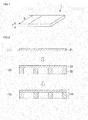
- Fig. 1 is a perspective view showing an embodiment of a fired piezoelectric body.
- Fig. 2 is a cross-sectional view showing an embodiment of a method for manufacturing a piezoelectric element of the present invention, showing the steps (1) to (3).
- Fig. 3 is a cross-sectional view showing an embodiment of a method for manufacturing a piezoelectric element of the present invention, showing the steps (I) to (VIII).
- Fig. 4 is a plan view (top view) showing an embodiment of a method for manufacturing a piezoelectric element of the present invention, showing the step (VII) in Fig. 3 .
- Fig. 5 is a plan view (top view) showing another embodiment of a method for manufacturing a piezoelectric element of the present invention, corresponding to Fig. 4 .
- Fig. 6 is a plan view (top view) showing another embodiment of a method for manufacturing a piezoelectric element of the present invention, corresponding to Fig. 4 .
- Fig. 7 is plan view (top view) showing another embodiment of a method for manufacturing a piezoelectric element of the present invention, corresponding to Fig. 4 .
- a method for manufacturing a piezoelectric element of the present invention described below is a method for manufacturing plural piezoelectric elements at the same time.
- six elements are taken in the example of Fig. 4 described later, naturally, it is possible to take several tens or more in mass production.
- Fig. 4 which is a plan view
- Fig. 3 is a cross-sectional view.
- Fig. 3 showing the steps shows cross-sectional views each cut along a plane perpendicular to the longitudinal direction of a piezoelectric element.
- FIG. 3 shows a cross section cut along a horizontal direction (left to right direction) including piezoelectric elements in Fig. 4 .
- All the drawings including these drawings are schematic views drawn so that the manufacturing process can easily be understood, and, for example, it should naturally be understood that the thickness of the fired piezoelectric body and the thickness of the electrode are not described in a practically preferable state.
- a method for manufacturing a piezoelectric element of the present invention is a method for obtaining a piezoelectric element provided with a thin and flat fired piezoelectric body with no warpage, in the first place, a fired piezoelectric body will be described.
- the fired piezoelectric body 1 shown in Fig. 1 is a single layer piezoelectric body.
- the fired piezoelectric body 1 has an almost square planar shape, there is no particular limitation on the outer shape of the fired piezoelectric body. In consideration of productivity, it is desirable that the outer shape can be obtained by machining, and the shape is preferably a shape formed by straight lines, such as a polygon, particularly a square or a rectangle.
- the piezoelectric element may have a mode having both a film-shaped electrode formed on both the surfaces (outer two surfaces) of a fired piezoelectric body having a plural layer structure and a film-shaped electrode formed on a surface between single layers. That is, in the structure, a laminate structure of an electrode, a fired piezoelectric body, an electrode, a fired piezoelectric body, and an electrode may be repeated.
- the number of the lamination in this case is preferably 3 as the number of the fired piezoelectric bodies and 4 as the number of the electrode and may be more.
- a thin green sheet 21 is manufactured by the use of a piezoelectric material (see step (1) of Fig. 2 ).
- slurry is prepared by adding, for example, a binder, a solvent, a dispersant, a plasticizer, and the like to a ceramic powder of lead zirconate titanate or the like and mixing them.
- a green sheet having the aforementioned thickness is manufactured by a method such as a reverse roll coater method, a doctor blade method, or the like. Then, the green sheet is cut to have a green sheet 21 having a desired size.
- the green sheet 21 later functions as a fired piezoelectric body constituting a piezoelectric element.
- a binder, a solvent, a dispersant, a plasticizer, and the like are added to a ceramic powder of lead zirconate titanate or the like, and they are mixed to have a paste, and reinforcers 22 having a desired thickness are formed on the green sheet 21 by screen printing (see the step (2) of Fig. 2 ).
- the reinforcer-provided fired piezoelectric body 23 means that the reinforcers 22 for firing and the green sheet 21 are unitarily fired.
- the through-holes 11 are made in the reinforcer-provided fired piezoelectric body 23 by the use of, for example, a laser (see the step (II) of Fig. 3 ).
- the through-holes 11 may be made before manufacturing the reinforcer-provided fired piezoelectric body 23.
- the reinforcer-provided fired piezoelectric body 23 can be obtained by forming a green sheet 21 having the through-holes 11 on, for example, a PET (polyethylene telephthalate) film by screen printing; by forming the reinforcers 22 on the green sheet 21 by screen printing; and by firing them at appropriate temperature of 800 to 1300°C on the basis of the piezoelectric material to be used in a state of having through-holes.
- film-shaped electrodes 33 and 34 made of the conductive material are formed on both the surfaces of the reinforcer-provided fired piezoelectric body 23 having through-holes 11 therein and in the through-holes 11 (see the step (III) of Fig. 3 ).
- the electrodes 33 and 34 can be formed by a sputtering treatment.
- the patterning may be performed by laser processing.
- Some parts of the reinforcer-provided fired piezoelectric body 23 and electrodes 33 and 34 are cut off by, for example, wet etching or blasting (see the step (Vi) of Fig. 3 ), and the resist 38 is removed by, for example, a remover to obtain piezoelectric element precursors 100B having a desired shape (see the step (VII) of Fig. 3 and Fig. 4 ) .
- Each of the piezoelectric element precursors 100B functions as a piezoelectric element later and is composed of a fired piezoelectric body 1 (obtained by removing the reinforcers and the like from the reinforcer-provided fired piezoelectric body 23) and electrodes 33 and 34.
- each of the piezoelectric element precursors 100B is taken out to be able to ship it as a piezoelectric element 100.
- An example of the desired shape is the shape of the piezoelectric element precursor 100B (see Fig. 4 ) though there is no limitation on the shape.
- the piezoelectric element precursor 100B Before the polarization treatment, it is important that the piezoelectric element precursor 100B has bonding portions 41, 42 (see Fig. 4 ) .
- the bonding portions 41, 42 are bonded to the portions not functioning as the piezoelectric element later (frame) in the reinforcer-provided fired piezoelectric body 23. Strictly speaking, the bonding portions 41, 42 are portions where the fired piezoelectric body 1 constituting the piezoelectric element precursor 100B is bonded to the frame.
- parts of the reinforcer-provided fired piezoelectric body 23 and electrodes 33, 34 are cut off so that the bonding portions 41, 42 are provided.
- the piezoelectric element precursors 100B Before the polarization, the piezoelectric element precursors 100B are not separated from one another.
- a power source is connected to the electrodes 33, 34 of the piezoelectric element precursor 100B, and, for example, a voltage of 1 to 16 kV/mm is applied to the fired piezoelectric body 1 of the piezoelectric element precursor 100B in the ambient atmosphere for 1 to 30 minutes to polarize the fired piezoelectric body 1.
- the polarization direction is the direction from the electrode 33 toward the electrode 34 (or the opposite direction).
- the direction is the thickness direction of the piezoelectric element precursor 100B (fired piezoelectric body 1).
- the direction perpendicular to the polarization direction is the surface direction of the piezoelectric element precursor 100B (fired piezoelectric body 1).
- the piezoelectric element precursor 100B (fired piezoelectric body 1) bonded to the frame (portions not functioning as the piezoelectric element 100 later in the reinforcer-provided fired piezoelectric body 23) by the bonding portions 41, 42 is fixed at two positions of the bonding portions 41, 42 in a direction perpendicular to the polarization direction during the polarization treatment.
- the bonding portions 41, 42 can be defined as fixed portions during the polarization treatment. Since the piezoelectric element precursor 100B (fired piezoelectric body 1) is long in the vertical direction in Fig. 4 , the positions where the piezoelectric element precursor 100B (fired piezoelectric body 1) is fixed (fixed portions) are located at both the ends in the longitudinal direction of the piezoelectric element precursor 100B (fired piezoelectric body 1).
- the piezoelectric element precursors 100B become usable (capable of displacement) piezoelectric elements 100. Then, necessary property tests are performed, and cutting is performed at bonding portions 41, 42 by the use of, for example, a laser beam machine to obtain each piezoelectric element 1 (see the step (VIII) of Fig. 3 ). Through washing, final inspection (confirmation of appearance and size), the piezoelectric elements 100 can be shipped.
- the piezoelectric element precursor has the bonding portions 53a, 53b or the bonding portions 63a, 63b in addition to the bonding portions 41 and 42.
- the piezoelectric element precursor (fired piezoelectric body) is fixed at four positions of the bonding portions 41, 42, 53a, and 53b or four positions of 41, 42, 63a, and 63b.
- the piezoelectric element precursors 100B are connected to the frame (portions not functioning as the piezoelectric elements 100 later among the reinforcer-provided fired piezoelectric body 23) perpendicularly to the sides of each piezoelectric element precursor 100B. However, they may obliquely be connected to the frame as in Fig. 6 .
- the piezoelectric element precursor (fired piezoelectric body) is fixed at three portions of bonding portions 41, 42a, and 42b in a direction perpendicular to the polarization direction during the polarization treatment.
- the through-holes 73 are formed so that the frame is separated in two directions, viewed from the bonding portions 42a, 42b.
- the piezoelectric element precursor (fired piezoelectric body) is definitely fixed at three positions of the bonding portions 41, 42a, and 42b in the direction perpendicular to the polarization direction during the polarization treatment.
- the fired piezoelectric body (piezoelectric element precursor) is fixed by holding the fired piezoelectric body (piezoelectric element precursor) from two directions at the two bonding portions 42a, 42b (fixed portions)
- the internal stress (deformation stress) to try to cause warpage generated by the polarization can be converted into elongation and deflection deformation in the two directions.
- A is defined as the width of the piezoelectric element precursor
- B is defined as the width of each of the bonding portions 42a and 42b
- C is defined as the width between the through-holes 73 and 74, it is preferable to have relations of A>B and A>C.
- an internal electrode (electrode to be put between the fired piezoelectric bodies) is separately formed on a green sheet by screen printing or the like.
- the green sheet is bonded to the aforementioned green sheet 21 (see the step (1) of Fig. 2 ) in such a manner that the surface having the electrode thereon is located between the sheets to manufacture a laminated green sheet (This step is repeated in the case of three or more layers.).
- the aforementioned reinforcers 22 are formed on the laminated green sheet by screen printing.
- a multilayer piezoelectric body can be obtained.
- a through-hole or a via-electrode may be formed in the green sheet 21.
- the material for the piezoelectric element will hereinbelow be described.
- the material (piezoelectric material) for the fired piezoelectric body as long as the material causes strain induced by an electric field by the reverse piezoelectric effect or the like and needs polarization.
- the material can suitably be selected from piezoelectric materials and ferroelectric ceramics depending on the use.
- the material include lead zirconate, lead titanate, lead magnesium niobate, lead nickel niobate, lead nickel tantalate, lead zinc niobate, lead manganese niobate, lead antimony stannate, lead antimony niobate, lead ytterbium niobate, lead manganese tungstate, lead cobalt niobate, lead magnesium tungstate, lead magnesium tantalate, barium titanate, sodium bismuth titanate, bismuth neodymium titanate (BNT), potassium sodium niobate, strontium bismuth tantalate, copper tungsten barium, bismuth ferrate, and a composite oxide of two or more of them.
- BNT bismuth neodymium titanate
- An oxide of rare earth element, calcium, strontium, molybudenum, tungsten, barium, niobium, zinc, nickel, manganese, cadmium, chromium, cobalt, antimony, iron, tantalum, lithium, bismuth, tin, copper, or the like may be added to the above material or substituted for the oxide part of the above material.
- a material obtained by substituting strontium for a part of lead and substituting niobium for a part of zirconium and/or titanium in a composite oxide of lead zirconate and lead titanate can preferably exhibit high material characteristics.
- a material obtained by adding, to the above material, lithium bismuthate, lithium borate, lithium carbonate, lead germanate or the like can further preferably exhibit high material property while realizing the firing of the piezoelectric body at low temperature.
- the aforementioned piezoelectric material can be used also for the reinforcers. It is preferable to use the same material as that for the fired piezoelectric body to have the same thermal expansion.
- a conductive metal is employed as the material for the electrode.
- the conductive metal include single metals of aluminum, titanium, chromium, iron, cobalt, nickel, copper, zinc, niobium, molybdenum, ruthenium, palladium, rhodium, silver, tin, tantalum, tungsten, iridium, platinum, gold, or lead; or alloys of two or more of them, for example, silver-platinum, platinum-palladium, and silver-palladium, which may be used alone or as a combination of two or more of them.
- cermet there may be used a cermet, a mixture of these materials with aluminum oxide, zirconium oxide, titanium oxide, silicon oxide, cerium oxide, glass, or a piezoelectric material.
- the material may be selected in accordance with the kind of the piezoelectric material.
- a piezoelectric element precursor fixed by three bonding portions as one piezoelectric element precursor in Fig. 7 was manufactured according to a method for manufacturing a piezoelectric element of the present invention. Specifically, in the first place, there was obtained a fired piezoelectric body having a rectangular shape of 2 mm x 4 mm and a thickness of 15 ⁇ m. Thethickness of the fired piezoelectric body was 15 ⁇ m, and the surface roughness Ra was 0.19 ⁇ m on one surface of the fired piezoelectric body while it was 0.1 ⁇ m on the other surface.
- the piezoelectric material there was used 0.17Pb (Mg1/3Nb2/3) O 3 -0.03Pb (Ni1/3Nb2/3) O 3 -0.43PbTi O 3 - 0.37PbZrO 3 .
- the same piezoelectric material was used for the reinforcers (corresponding to the reinforcers 22 of the step (2) of Fig. 2 ) for firing, and the reinforcers were formed by screen printing to have a thickness of 30 ⁇ m.
- the firing was performed at 1200°C for two hours.
- Gold (Au) was used for the electrode, which was formed by sputtering. After the electrode was formed, a piezoelectric element precursor was obtained by blasting.
- a piezoelectric element was obtained by polarization by applying a voltage of 5 kV/mm to the still fixed piezoelectric element precursor for 15 minutes in room temperature (in the atmosphere).
- the undulation amount for 10 elements was measured by the use of a laser displacement gauge (LK-G5000) produced by Keyence, and it was 0.2 to 3 ⁇ m. Then, a drive durability test was performed by a rectangular wave of 10V at 5 kHz for one hour to confirm that no problem was caused.
- Example 2 There was manufactured a piezoelectric element precursor having no fixing, and polarization was performed in the same manner as in Example 1 except for the aforementioned point to obtain a piezoelectric element.
- the undulation amount for 10 elements was measured, and it was 100 to 500 ⁇ m.
- a method for manufacturing a piezoelectric element of the present invention can suitably be used as a means for manufacturing a piezoelectric element provided on various piezoelectric actuators (piezoelectric devices) applied to measuring instruments, optical modulators, optical switches, microvalves, carrier devices, image displays (display, projector, etc.), image drawing instruments, micropumps, droplet ejectors, micromixers, microstirrers, and microreactors; or various piezoelectric sensors (piezoelectric devices) used for detecting fluid properties, sound pressure, microweight, acceleration, and the like.
Landscapes
- Engineering & Computer Science (AREA)
- Manufacturing & Machinery (AREA)
- Particle Formation And Scattering Control In Inkjet Printers (AREA)
- General Electrical Machinery Utilizing Piezoelectricity, Electrostriction Or Magnetostriction (AREA)
- Micromachines (AREA)
- Piezo-Electric Or Mechanical Vibrators, Or Delay Or Filter Circuits (AREA)
- Piezo-Electric Transducers For Audible Bands (AREA)
Abstract
Description
- The present invention relates to a method for manufacturing a piezoelectric element provided with a thin and flat fired piezoelectric body with no warpage.
- Recently, there has been desired a displacement control device capable of adjusting the optical path length and position in submicrometer in the fields of optics, precision machinery, semiconductormanufacturing, etc. In response to this, there is proceeding development of piezoelectric devices such as a piezoelectric actuator utilizing strain (displacement, change in shape) based on the reverse piezoelectric effect caused upon applying an electric field to a piezoelectric body and a piezoelectric sensor utilizing charge generation (polarization) caused upon applying stress to a piezoelectric body on the basis of a piezoelectric effect.
- The core of these piezoelectric devices is a piezoelectric element obtained by putting a piezoelectric body between electrodes. Of these, the piezoelectric body can be manufactured by forming a piezoelectric material into a film shape by a thin film method and firing it at high temperature (hereinbelow, a piezoelectric body obtained in this way is referred to as a fired piezoelectric body) . Since, in the fired piezoelectric body, the direction of intrinsic polarization (bias of charge) is not oriented if the fired piezoelectric body is left as it is, almost no strain is generated, and it cannot be used as a piezoelectric element.
- Therefore, in a manufacturing process of a piezoelectric element formed by putting a fired piezoelectric body between electrodes, the piezoelectric element is generally subjected to a polarization treatment. The polarization treatment is generally performed just before the final step of cleaning or the like. The target of the polarization treatment is naturally the fired piezoelectric body constituting the piezoelectric element. The polarization treatment is generally performed by applying a voltage of several kV/mm for about several tens of minutes in the atmosphere or in a liquid. In the polarized fired piezoelectric body (piezoelectric element), the direction of the intrinsic polarization is oriented to almost the same direction and is not reposited to have a polarization value (remnant polarization) even without applying any voltage. Then, a voltage is applied to this (an electric field is applied), strain (displacement, deformation) is generated on the basis of the amount of the voltage.
- An example of the prior art document relating to the polarization of a piezoelectric body (piezoelectric porcelain) is
JP-2004-296783 JP-2004-296783 - By the way, in accordance with downsizing, thinning, and energy saving of electronic devices in recent years, thinning and downsizing are required for a piezoelectric device mounted on the electronic devices and a piezoelectric element constituting the piezoelectric device. In addition, a piezoelectric device (piezoelectric actuator) may employ a structure where a piezoelectric element is bonded to a metal board as described in
JP-2001-068751 - However, since a thin fired piezoelectric body can be obtained through processing and firing, there is easily generated a difference in the crystal orientation degree, the crystal formation, or the intrinsic polarization state between the front and back surfaces of the fired piezoelectric body in the process prior to processing and firing. Therefore, warpage is caused upon the polarization treatment, and it is difficult to obtain a flat fired piezoelectric body (piezoelectric element) with no warpage after the polarization treatment. In addition, for example, if the polarization treatment is performed with applying a compression force parallel to the polarization direction according to the polarization method disclosed in
JP-A-2004-296783 - The present invention has been made in view of the aforementioned circumstances and aims to provide a means for obtaining a piezoelectric element provided with a thin and flat fired piezoelectric body with no warpage and no breakage. As a result of repeated study, it has been found out that the problems can be solved by polarizing the fired piezoelectric body (piezoelectric element) while fixing it at least two positions (from two directions) in a direction perpendicular to the polarization direction.
- That is, in the first place, according to the present invention, there is provided a method for manufacturing a piezoelectric element having a thin board-shaped fired piezoelectric body and a film-shaped electrode formed on both the surfaces of the fired piezoelectric body; wherein the method has a step of polarizing the fired piezoelectric body while fixing it at least two positions in a direction perpendicular to the polarization direction.
- The step of polarizing the fired piezoelectric body (polarization treatment step) is generally located at almost the end of the entire manufacturing process for a piezoelectric element. The piezoelectric element before the polarization may be manufactured by any means. The polarization direction means a direction (orientation) of the intrinsic polarization to be oriented. The polarization direction is generally perpendicular to the surface direction of a pair of electrodes facing each other, and, in the case of a thin board-shaped fired piezoelectric body, since a pair of electrodes are formed on the surface perpendicular to the thickness direction of the fired piezoelectric body, the thickness direction serves as the polarization direction. In addition, in this case, the direction perpendicular to the polarization direction is a surface direction of the electrode provided on the surface of the thin board-shaped fired piezoelectric body. Therefore, the positions where the fired piezoelectric body is fixed are in a surface direction of the thin board-shaped fired piezoelectric body. Preferably, the positions where the fired piezoelectric body is fixed are the end portions of the thin board-shaped fired piezoelectric body.
- In addition, in a method for manufacturing a piezoelectric element of the present invention, it is preferable that the thin board-shaped fired piezoelectric body is fixed at both the ends in the longitudinal direction of the fired piezoelectric body.
- The longitudinal direction of the thin board-shaped fired piezoelectric body means the direction where the distance from one end to the other end through the gravity center is the longest when the thin board-shaped fired piezoelectric body is considered as a plane shape . When the thin board-shaped fired piezoelectric body is circular, the longitudinal direction is not specified, and, when it is square, the longitudinal direction is not specified as long as the direction is limited to the direction of a side . However, in the other cases, the direction is specified.
- Inamethodformanufacturingapiezoelectric element of the present invention, it is preferable that the fired piezoelectric body is fixed by holding the fired piezoelectric body from plural directions for one fixed portion at the positions where the thin board-shaped fired piezoelectric body is fixed.
- Holding the fired piezoelectric body from plural directions for one fixed portion means the mode where the portion holding the fired piezoelectric body is separated at the positions where the fired piezoelectric body is fixed.
- In a method for manufacturing a piezoelectric element of the present invention, it is preferable that the positions where the thin board-shaped fired piezoelectric body is fixed are cut after the polarization. In this case, the cutting means is preferably one selected from the means consisting of an electron beam, an ion beam, etching, blasting, and laser processing.
- Next, according to the present invention, there is provided a method for polarizing a fired piezoelectric body, where the thin board-shaped fired piezoelectric body is fixed at least two positions in a direction perpendicular to the polarization direction to polarize the fired piezoelectric body.
- Inamethodformanufacturingapiezoelectric element of the present invention and in a method for polarizing a fired piezoelectric body of the present invention, the polarization treatment is performed by applying a voltage of several kV/mm for about several tens minutes in the ambient atmosphere or in a liquid. Preferably, it is performed by applying a voltage of 1 to 16 kV/mm for about 1 to 30 minutes in the ambient atmosphere. A more preferable voltage is 2 to 10 kV/mm, and more preferable time of application is 5 to 20 minutes.
- Incidentally, in the present specification, piezoelectric or piezoelectric body is referred. An object made of a material exhibiting strain induced by an electric field and requiring a polarization treatment is included in the piezoelectric body. Generally, almost all the objects made of ferroelectric material are included in this. However, an object made of an electrostrictive material which does not require a polarization treatment is excluded.
- In a method for manufacturing a piezoelectric element of the present invention and a polarization method of the fired piezoelectric body of the present invention, since the fired piezoelectric body is polarized by being fixed at least two positions in a direction perpendicular to the polarization direction, warpage is hardly caused even though the fired piezoelectric body is thin board-shaped to be able to obtain a flat fired piezoelectric body (piezoelectric element). The fired piezoelectric body (piezoelectric element) is not destroyed during the polarization treatment, and a polarized piezoelectric element (fired piezoelectric body) can be manufactured well. This is because, by the fixing at two or more positions in a direction perpendicular to the polarization direction, the deformation is suppressed, and the internal stress (deformation stress) generated by polarization and trying to deform is converted into elongation and deflection deformation in the fixed portions at the two or more positions.
- The aforementioned effect can stably be obtained when the fixing is performed at three or more positions in the direction perpendicular to the polarization direction in comparison with the case of two positions. That is, there can be obtained a more flat (excellent in flatness) fired piezoelectric body (piezoelectric element) with hardly having warpage and with less damages such as a crack after the polarization treatment. However, since the fixing positions (fixed portions) shouldbe cut later, the manufacturing process becomes complex. Therefore, it is particularly preferable to fix the fired piezoelectric body at two to four positions in accordance with the shape of the electrode.
- The aforementioned effect can be obtained wherever the positions for fixing the thin board-shaped fired piezoelectric body are located in comparison with a method excluded from the methods for manufacturing a piezoelectric element of the present invention. However, in a method for manufacturing a piezoelectric element of the present invention, since the positions where the thin board-shaped fired piezoelectric body is fixed are at both the ends in the longitudinal direction of the fired piezoelectric body in a preferable mode, the aforementioned effect can stably be obtained in comparison with a case different from this mode. That is, the fired piezoelectric body (piezoelectric element) is more flat (excellent in flatness) with hardly generating warpage. The possibility of having damages in a fired piezoelectric body (piezoelectric element) during the polarization treatment is reduced.
- Since, in a method for manufacturing a piezoelectric element of the present invention, the fired piezoelectric body is fixed by holding the fired piezoelectric body from plural directions (at one position) in positions where the thin board-shaped fired piezoelectric body is fixed in a preferable mode, the aforementioned effect can stably be obtained in comparison with a case different from this mode. That is, the fired piezoelectric body (piezoelectric element) is more flat (excellent in flatness) with hardly generating warpage. The possibility of having damages in a fired piezoelectric body (piezoelectric element) during the polarization treatment is reduced. This is because the internal stress (deformation stress) generated by polarization and trying to deform is converted into elongation and deflection deformation in the fixed portions other than the portion to be a piezoelectric element in a direction perpendicular to the polarization direction and portions held from plural directions.
- Since, in a method for manufacturing a piezoelectric element of the present invention, the positions where the thin board-shaped fired piezoelectric body is fixed are cut after the polarization in a preferable mode, a flat piezoelectric element having little warpage can be obtained. That is, since no stress due to polarization remains, it is possible to obtain a piezoelectric element in the same state as the fixed state even after the fixed positions are cut off. In addition, if the means for cutting is one selected from the means consisting of an electron beam, an ion beam, etching, blasting, and laser processing, it is possible to cut the fixed positions in a state of having less processing stress to the piezoelectric element than the other means and to obtain a piezoelectric element having little warpage and the like.
- [
Fig. 1] Fig. 1 is a perspective view showing an embodiment of a fired piezoelectric body. - [
Fig. 2] Fig. 2 is a cross-sectional view showing an embodiment of a method for manufacturing a piezoelectric element of the present invention, showing the steps (1) to (3). - [
Fig. 3] Fig. 3 is a cross-sectional view showing an embodiment of a method for manufacturing a piezoelectric element of the present invention, showing the steps (I) to (VIII). - [
Fig. 4] Fig. 4 is a plan view (top view) showing an embodiment of a method for manufacturing a piezoelectric element of the present invention, showing the step (VII) inFig. 3 . - [
Fig. 5] Fig. 5 is a plan view (top view) showing another embodiment of a method for manufacturing a piezoelectric element of the present invention, corresponding toFig. 4 . - [
Fig. 6] Fig. 6 is a plan view (top view) showing another embodiment of a method for manufacturing a piezoelectric element of the present invention, corresponding toFig. 4 . - [
Fig. 7] Fig. 7 is plan view (top view) showing another embodiment of a method for manufacturing a piezoelectric element of the present invention, corresponding toFig. 4 . Reference Numerals - 1: fired piezoelectric body, 11: through-hole, 21: green sheet, 22: reinforcer, 23: reinforcer-provided fired piezoelectric body, 33: electrode, 34: electrode, 38: resist, 39: resin, 41: bonding portion, 42: bonding portion, 42a: bonding portion, 42b: bonding portion, 53a: bonding portion, 53b: bonding portion, 63a: bonding portion, 63b: bonding portion, 73: through-hole, 74: through-hole, 100: piezoelectric element, 100B: piezoelectric element precursor
- Embodiments of the present invention will be described with appropriately referring to drawings. However, the present invention should not be construed with limiting to these embodiments, and various changes, modifications, and improvements may be made on the basis of knowledge of a person of ordinary skill in the art as long as they do not deviate from the scope of the present invention. For example, though the drawings show preferable embodiments of the present invention, the present invention is by no means limited to the modes shown by the drawings or information shown by the drawings. In carrying out or examining the present invention, though the same means as or a means equivalent to a means described in the present specification can be applied, a suitable means is a means described below.
- Incidentally, a method for manufacturing a piezoelectric element of the present invention described below is a method for manufacturing plural piezoelectric elements at the same time. Though six elements are taken in the example of
Fig. 4 described later, naturally, it is possible to take several tens or more in mass production. In addition, though the state of the step (VII) inFig. 3 is shown inFig. 4 , which is a plan view, whereasFig. 3 is a cross-sectional view.Fig. 3 showing the steps shows cross-sectional views each cut along a plane perpendicular to the longitudinal direction of a piezoelectric element. In otherwords, the step (VII) ofFig. 3 shows a cross section cut along a horizontal direction (left to right direction) including piezoelectric elements inFig. 4 . All the drawings including these drawings are schematic views drawn so that the manufacturing process can easily be understood, and, for example, it should naturally be understood that the thickness of the fired piezoelectric body and the thickness of the electrode are not described in a practically preferable state. - Since a method for manufacturing a piezoelectric element of the present invention is a method for obtaining a piezoelectric element provided with a thin and flat fired piezoelectric body with no warpage, in the first place, a fired piezoelectric body will be described. The fired
piezoelectric body 1 shown inFig. 1 is a single layer piezoelectric body. Though the firedpiezoelectric body 1 has an almost square planar shape, there is no particular limitation on the outer shape of the fired piezoelectric body. In consideration of productivity, it is desirable that the outer shape can be obtained by machining, and the shape is preferably a shape formed by straight lines, such as a polygon, particularly a square or a rectangle. - Though a piezoelectric element obtained by a method for manufacturing a piezoelectric element of the present invention is not illustrated, it is obtained by forming a film-shaped electrode on both the surfaces of the fired
piezoelectric body 1 shown inFig. 1 . The piezoelectric element may have a mode having both a film-shaped electrode formed on both the surfaces (outer two surfaces) of a fired piezoelectric body having a plural layer structure and a film-shaped electrode formed on a surface between single layers. That is, in the structure, a laminate structure of an electrode, a fired piezoelectric body, an electrode, a fired piezoelectric body, and an electrode may be repeated. The number of the lamination in this case is preferably 3 as the number of the fired piezoelectric bodies and 4 as the number of the electrode and may be more. - An embodiment of a method for manufacturing a piezoelectric element of the present invention will be described. In a method for manufacturing a fired piezoelectric body of the present invention, a thin
green sheet 21 is manufactured by the use of a piezoelectric material (see step (1) ofFig. 2 ). Specifically, slurry is prepared by adding, for example, a binder, a solvent, a dispersant, a plasticizer, and the like to a ceramic powder of lead zirconate titanate or the like and mixing them. After the slurry is subjected to a defoaming treatment, a green sheet having the aforementioned thickness is manufactured by a method such as a reverse roll coater method, a doctor blade method, or the like. Then, the green sheet is cut to have agreen sheet 21 having a desired size. Thegreen sheet 21 later functions as a fired piezoelectric body constituting a piezoelectric element. - Then, a binder, a solvent, a dispersant, a plasticizer, and the like are added to a ceramic powder of lead zirconate titanate or the like, and they are mixed to have a paste, and
reinforcers 22 having a desired thickness are formed on thegreen sheet 21 by screen printing (see the step (2) ofFig. 2 ). - Subsequently, they are fired at an appropriate temperature of 800 to 1300°C on the basis of the piezoelectric material to be used to obtain a reinforcer-provided fired piezoelectric body 23 (see the step (3) of
Fig. 2 and the step (I) ofFig. 3 ). The reinforcer-provided firedpiezoelectric body 23 means that thereinforcers 22 for firing and thegreen sheet 21 are unitarily fired. - Though-
holes 11 are made in the reinforcer-provided firedpiezoelectric body 23 by the use of, for example, a laser (see the step (II) ofFig. 3 ). The through-holes 11 may be made before manufacturing the reinforcer-provided firedpiezoelectric body 23. In this case, the reinforcer-provided firedpiezoelectric body 23 can be obtained by forming agreen sheet 21 having the through-holes 11 on, for example, a PET (polyethylene telephthalate) film by screen printing; by forming thereinforcers 22 on thegreen sheet 21 by screen printing; and by firing them at appropriate temperature of 800 to 1300°C on the basis of the piezoelectric material to be used in a state of having through-holes. - Then, by performing, for example, resist patterning and by applying the paste of a conductive material (e.g., gold), film-shaped
electrodes piezoelectric body 23 having through-holes 11 therein and in the through-holes 11 (see the step (III) ofFig. 3 ). Theelectrodes - Thereinforcer-providedfired
piezoelectric body 23 is further reinforced, and resist patterning is performed to impart a desired shape to the portions functioning as piezoelectric elements (piezoelectric element precursors) later. Specifically,resin 39 is filled into the spaces between the reinforcers of the reinforcer-provided fired piezoelectric body 23 (see the step (IV) ofFig. 3 ). Then, the resist 38 is applied by, e.g., a light exposure method to the surface of the reinforcer-provided firedpiezoelectric body 23 excluding the portion to be removed (see the step (V)) ofFig. 3 ). Theresin 39 may be filled into the spaces between the reinforcers after the resist 38 is applied. Some parts of the reinforcer-provided firedpiezoelectric body 23 andelectrodes Fig. 3 ), and the resist 38 is removed by, for example, a remover to obtainpiezoelectric element precursors 100B having a desired shape (see the step (VII) ofFig. 3 andFig. 4 ) . Each of thepiezoelectric element precursors 100B functions as a piezoelectric element later and is composed of a fired piezoelectric body 1 (obtained by removing the reinforcers and the like from the reinforcer-provided fired piezoelectric body 23) andelectrodes piezoelectric element precursors 100B is taken out to be able to ship it as apiezoelectric element 100. An example of the desired shape is the shape of thepiezoelectric element precursor 100B (seeFig. 4 ) though there is no limitation on the shape. - Before the polarization treatment, it is important that the
piezoelectric element precursor 100B hasbonding portions 41, 42 (seeFig. 4 ) . Thebonding portions piezoelectric body 23. Strictly speaking, thebonding portions piezoelectric body 1 constituting thepiezoelectric element precursor 100B is bonded to the frame. In other words, upon obtaining thepiezoelectric element precursors 100B, parts of the reinforcer-provided firedpiezoelectric body 23 andelectrodes bonding portions piezoelectric element precursors 100B are not separated from one another. - A power source is connected to the
electrodes piezoelectric element precursor 100B, and, for example, a voltage of 1 to 16 kV/mm is applied to the firedpiezoelectric body 1 of thepiezoelectric element precursor 100B in the ambient atmosphere for 1 to 30 minutes to polarize the firedpiezoelectric body 1. At this time, the polarization direction is the direction from theelectrode 33 toward the electrode 34 (or the opposite direction). The direction is the thickness direction of thepiezoelectric element precursor 100B (fired piezoelectric body 1). In addition, the direction perpendicular to the polarization direction is the surface direction of thepiezoelectric element precursor 100B (fired piezoelectric body 1). Therefore, thepiezoelectric element precursor 100B (fired piezoelectric body 1) bonded to the frame (portions not functioning as thepiezoelectric element 100 later in the reinforcer-provided fired piezoelectric body 23) by thebonding portions bonding portions - The
bonding portions piezoelectric element precursor 100B (fired piezoelectric body 1) is long in the vertical direction inFig. 4 , the positions where thepiezoelectric element precursor 100B (fired piezoelectric body 1) is fixed (fixed portions) are located at both the ends in the longitudinal direction of thepiezoelectric element precursor 100B (fired piezoelectric body 1). - Through the aforementioned steps, the
piezoelectric element precursors 100B become usable (capable of displacement)piezoelectric elements 100. Then, necessary property tests are performed, and cutting is performed atbonding portions Fig. 3 ). Through washing, final inspection (confirmation of appearance and size), thepiezoelectric elements 100 can be shipped. - As shown in
Figs. 5 and6 , it is preferable that the piezoelectric element precursor has thebonding portions bonding portions bonding portions bonding portions Fig. 5 , thepiezoelectric element precursors 100B are connected to the frame (portions not functioning as thepiezoelectric elements 100 later among the reinforcer-provided fired piezoelectric body 23) perpendicularly to the sides of eachpiezoelectric element precursor 100B. However, they may obliquely be connected to the frame as inFig. 6 . - AsshowninFig. 7, it is preferable to provide through-
holes piezoelectric elements 100 later in the reinforcer-provided fired piezoelectric body 23) in the vicinity of thebonding portions 42. By the presence of the through-hole 74, the piezoelectric element precursor (fired piezoelectric body) is fixed at three portions ofbonding portions holes 73 are formed so that the frame is separated in two directions, viewed from thebonding portions bonding portions bonding portions bonding portions holes - The case of a single layer fired piezoelectric body has been described. In the case that the fired piezoelectric body has two or more layers, in the first place, an internal electrode (electrode to be put between the fired piezoelectric bodies) is separately formed on a green sheet by screen printing or the like. The green sheet is bonded to the aforementioned green sheet 21 (see the step (1) of
Fig. 2 ) in such a manner that the surface having the electrode thereon is located between the sheets to manufacture a laminated green sheet (This step is repeated in the case of three or more layers.). Then, the aforementioned reinforcers 22 (see the step (2) ofFig. 2 ) are formed on the laminated green sheet by screen printing. Through the steps shown inFig. 3 , a multilayer piezoelectric body can be obtained. At this time, in order to have conduction with the internal electrode, a through-hole or a via-electrode may be formed in thegreen sheet 21. - The material for the piezoelectric element will hereinbelow be described. There is no particular limitation on the material (piezoelectric material) for the fired piezoelectric body as long as the material causes strain induced by an electric field by the reverse piezoelectric effect or the like and needs polarization. The material can suitably be selected from piezoelectric materials and ferroelectric ceramics depending on the use.
- Preferable examples of the material include lead zirconate, lead titanate, lead magnesium niobate, lead nickel niobate, lead nickel tantalate, lead zinc niobate, lead manganese niobate, lead antimony stannate, lead antimony niobate, lead ytterbium niobate, lead manganese tungstate, lead cobalt niobate, lead magnesium tungstate, lead magnesium tantalate, barium titanate, sodium bismuth titanate, bismuth neodymium titanate (BNT), potassium sodium niobate, strontium bismuth tantalate, copper tungsten barium, bismuth ferrate, and a composite oxide of two or more of them. An oxide of rare earth element, calcium, strontium, molybudenum, tungsten, barium, niobium, zinc, nickel, manganese, cadmium, chromium, cobalt, antimony, iron, tantalum, lithium, bismuth, tin, copper, or the like may be added to the above material or substituted for the oxide part of the above material. Among these materials, a material obtained by substituting strontium for a part of lead and substituting niobium for a part of zirconium and/or titanium in a composite oxide of lead zirconate and lead titanate can preferably exhibit high material characteristics. A material obtained by adding, to the above material, lithium bismuthate, lithium borate, lithium carbonate, lead germanate or the like can further preferably exhibit high material property while realizing the firing of the piezoelectric body at low temperature.
- The aforementioned piezoelectric material can be used also for the reinforcers. It is preferable to use the same material as that for the fired piezoelectric body to have the same thermal expansion.
- As the material for the electrode, a conductive metal is employed. Preferable examples of the conductive metal include single metals of aluminum, titanium, chromium, iron, cobalt, nickel, copper, zinc, niobium, molybdenum, ruthenium, palladium, rhodium, silver, tin, tantalum, tungsten, iridium, platinum, gold, or lead; or alloys of two or more of them, for example, silver-platinum, platinum-palladium, and silver-palladium, which may be used alone or as a combination of two or more of them. There may be used a cermet, a mixture of these materials with aluminum oxide, zirconium oxide, titanium oxide, silicon oxide, cerium oxide, glass, or a piezoelectric material. The material may be selected in accordance with the kind of the piezoelectric material.
- Hereinbelow, the present invention will be described in more detail with referring to Examples. However, the present invention is by no means limited to these Examples.
- A piezoelectric element precursor fixed by three bonding portions as one piezoelectric element precursor in
Fig. 7 was manufactured according to a method for manufacturing a piezoelectric element of the present invention. Specifically, in the first place, there was obtained a fired piezoelectric body having a rectangular shape of 2 mm x 4 mm and a thickness of 15 µm. Thethickness of the fired piezoelectric body was 15 µm, and the surface roughness Ra was 0.19 µm on one surface of the fired piezoelectric body while it was 0.1 µm on the other surface. As the piezoelectric material, there was used 0.17Pb (Mg1/3Nb2/3) O3-0.03Pb (Ni1/3Nb2/3) O3-0.43PbTi O3 - 0.37PbZrO3. The same piezoelectric material was used for the reinforcers (corresponding to thereinforcers 22 of the step (2) ofFig. 2 ) for firing, and the reinforcers were formed by screen printing to have a thickness of 30 µm. The firing was performed at 1200°C for two hours. Gold (Au) was used for the electrode, which was formed by sputtering. After the electrode was formed, a piezoelectric element precursor was obtained by blasting. - A piezoelectric element was obtained by polarization by applying a voltage of 5 kV/mm to the still fixed piezoelectric element precursor for 15 minutes in room temperature (in the atmosphere). The undulation amount for 10 elements was measured by the use of a laser displacement gauge (LK-G5000) produced by Keyence, and it was 0.2 to 3 µm. Then, a drive durability test was performed by a rectangular wave of 10V at 5 kHz for one hour to confirm that no problem was caused.
- There was manufactured a piezoelectric element precursor fixed by two bonding portions like one piezoelectric element precursor in
Fig. 4 , and polarization was performed in the same manner as in Example 1 except for the aforementioned point to obtain a piezoelectric element. The undulation amount for 10 elements was measured, and it was 0.5 to 30 µm. Then, a drive durability test was performed by a rectangular wave of 10V at 5 kHz for one hour to confirm that no problem was caused. - There was manufactured a piezoelectric element precursor having no fixing, and polarization was performed in the same manner as in Example 1 except for the aforementioned point to obtain a piezoelectric element. The undulation amount for 10 elements was measured, and it was 100 to 500 µm.
- A method for manufacturing a piezoelectric element of the present invention can suitably be used as a means for manufacturing a piezoelectric element provided on various piezoelectric actuators (piezoelectric devices) applied to measuring instruments, optical modulators, optical switches, microvalves, carrier devices, image displays (display, projector, etc.), image drawing instruments, micropumps, droplet ejectors, micromixers, microstirrers, and microreactors; or various piezoelectric sensors (piezoelectric devices) used for detecting fluid properties, sound pressure, microweight, acceleration, and the like.
Claims (6)
- A method for manufacturing a piezoelectric element having a thin board-shaped fired piezoelectric body and a film-shaped electrode formed on both the surfaces of the fired piezoelectric body;
wherein the method has a step of polarizing the fired piezoelectric body while fixing it at least two positions in a direction perpendicular to the polarization direction. - The method for manufacturing a piezoelectric element according to Claim 1, wherein the thin board-shaped fired piezoelectric body is fixed at both the ends in the longitudinal direction of the fired piezoelectric body.
- The method for manufacturing a piezoelectric element according to Claim 1 or 2, wherein the fired piezoelectric body is fixed by holding the fired piezoelectric body from plural directions at the positions where the thin board-shaped fired piezoelectric body is fixed.
- The method for manufacturing a piezoelectric element according to any one of Claims 1 to 3, wherein the positions where the thin board-shaped fired piezoelectric body is fixed are cut after the polarization.
- The method for manufacturing a piezoelectric element according to Claim 4, wherein the means for the cutting is one selected from the means consisting of an electron beam, an ion beam, etching, blasting, and laser processing.
- A method for polarizing a fired piezoelectric body, where the thin board-shaped fired piezoelectric body is fixed at least two positions in a direction perpendicular to the polarization direction to polarize the fired piezoelectric body.
Applications Claiming Priority (1)
| Application Number | Priority Date | Filing Date | Title |
|---|---|---|---|
| JP2010253013A JP5676216B2 (en) | 2010-11-11 | 2010-11-11 | Method for manufacturing piezoelectric element |
Publications (2)
| Publication Number | Publication Date |
|---|---|
| EP2453495A2 true EP2453495A2 (en) | 2012-05-16 |
| EP2453495A3 EP2453495A3 (en) | 2014-01-22 |
Family
ID=45047567
Family Applications (1)
| Application Number | Title | Priority Date | Filing Date |
|---|---|---|---|
| EP20110185317 Withdrawn EP2453495A3 (en) | 2010-11-11 | 2011-10-14 | Method for manufacturing piezoelectric element |
Country Status (4)
| Country | Link |
|---|---|
| US (1) | US9246081B2 (en) |
| EP (1) | EP2453495A3 (en) |
| JP (1) | JP5676216B2 (en) |
| CN (1) | CN102468423B (en) |
Families Citing this family (7)
| Publication number | Priority date | Publication date | Assignee | Title |
|---|---|---|---|---|
| US8981627B2 (en) * | 2012-06-04 | 2015-03-17 | Tdk Corporation | Piezoelectric device with electrode films and electroconductive oxide film |
| CN104956244B (en) * | 2013-02-01 | 2017-07-21 | 株式会社村田制作所 | Display panel with compression sensor and the electronic equipment with pressing input function |
| WO2016060072A1 (en) * | 2014-10-17 | 2016-04-21 | 株式会社村田製作所 | Piezoelectric device and method for manufacturing piezoelectric device |
| WO2016158743A1 (en) | 2015-03-30 | 2016-10-06 | 株式会社村田製作所 | Mother piezoelectric element, laminated piezoelectric element, and manufacturing method for laminated piezoelectric element |
| US10069061B2 (en) * | 2016-06-02 | 2018-09-04 | eLux Inc. | Fabrication and harvest of piezoelectric plates |
| CN109427958A (en) * | 2017-09-05 | 2019-03-05 | 王开安 | Membrane polarization bearing assembly and membrane polarization equipment |
| CN110467456A (en) * | 2019-09-16 | 2019-11-19 | 桂林电子科技大学 | A material with reversible thermo-optic modulation properties and its preparation method |
Citations (2)
| Publication number | Priority date | Publication date | Assignee | Title |
|---|---|---|---|---|
| JP2001068751A (en) | 1999-08-25 | 2001-03-16 | Murata Mfg Co Ltd | Piezo actuator |
| JP2004296783A (en) | 2003-03-27 | 2004-10-21 | Kyocera Corp | Polarization method and polarization device for piezoelectric ceramics |
Family Cites Families (16)
| Publication number | Priority date | Publication date | Assignee | Title |
|---|---|---|---|---|
| JPS5492307A (en) * | 1977-12-29 | 1979-07-21 | Sony Corp | Driving circuit of electrostrictive converter |
| DE3585938D1 (en) * | 1984-09-26 | 1992-06-04 | Terumo Corp | ULTRASONIC TRANSDUCER AND METHOD FOR PRODUCING THE SAME. |
| JPS6484675A (en) * | 1987-09-28 | 1989-03-29 | Fuji Rubber Co Ltd | Manufacture of piezoelectric element |
| JP3613140B2 (en) * | 1999-08-26 | 2005-01-26 | 株式会社村田製作所 | Piezoelectric ceramic composition and piezoelectric ceramic element using the same |
| US6953977B2 (en) * | 2000-02-08 | 2005-10-11 | Boston Microsystems, Inc. | Micromechanical piezoelectric device |
| CN100411214C (en) * | 2003-12-16 | 2008-08-13 | 松下电器产业株式会社 | Piezoelectric thin film device and driving method of piezoelectric thin film device |
| JP2005203750A (en) * | 2003-12-16 | 2005-07-28 | Matsushita Electric Ind Co Ltd | Piezoelectric thin film device and driving method of piezoelectric thin film device |
| JP2006203304A (en) * | 2005-01-18 | 2006-08-03 | Hitachi Media Electoronics Co Ltd | Piezoelectric thin film resonator, oscillator using the same, and semiconductor integrated circuit incorporating the same |
| ATE484851T1 (en) * | 2005-02-21 | 2010-10-15 | Brother Ind Ltd | METHOD FOR PRODUCING A PIEZOELECTRIC ACTUATOR |
| JP2006261656A (en) * | 2005-02-21 | 2006-09-28 | Brother Ind Ltd | Piezoelectric actuator and manufacturing method thereof |
| WO2006109501A1 (en) | 2005-03-18 | 2006-10-19 | Ngk Insulators, Ltd. | Piezoelectric element inspection method, inspection device, and polarization processing method |
| CN100555697C (en) * | 2005-06-29 | 2009-10-28 | 日本碍子株式会社 | Manufacturing method of piezoelectric/electrostrictive element |
| WO2007001063A1 (en) | 2005-06-29 | 2007-01-04 | Ngk Insulators, Ltd. | Piezoelectric/electrostriction film type element |
| WO2008081767A1 (en) * | 2006-12-27 | 2008-07-10 | Murata Manufacturing Co., Ltd. | Piezoelectric valve |
| WO2008102481A1 (en) * | 2007-02-21 | 2008-08-28 | Murata Manufacturing Co., Ltd. | Method for manufacturing piezoelectric resonator, and piezoelectric resonator |
| US8375538B2 (en) * | 2009-03-27 | 2013-02-19 | Ngk Insulators, Ltd. | Method for manufacturing piezoelectric actuator |
-
2010
- 2010-11-11 JP JP2010253013A patent/JP5676216B2/en not_active Expired - Fee Related
-
2011
- 2011-10-10 CN CN201110309740.XA patent/CN102468423B/en not_active Expired - Fee Related
- 2011-10-12 US US13/271,597 patent/US9246081B2/en not_active Expired - Fee Related
- 2011-10-14 EP EP20110185317 patent/EP2453495A3/en not_active Withdrawn
Patent Citations (2)
| Publication number | Priority date | Publication date | Assignee | Title |
|---|---|---|---|---|
| JP2001068751A (en) | 1999-08-25 | 2001-03-16 | Murata Mfg Co Ltd | Piezo actuator |
| JP2004296783A (en) | 2003-03-27 | 2004-10-21 | Kyocera Corp | Polarization method and polarization device for piezoelectric ceramics |
Also Published As
| Publication number | Publication date |
|---|---|
| JP5676216B2 (en) | 2015-02-25 |
| CN102468423A (en) | 2012-05-23 |
| JP2012104715A (en) | 2012-05-31 |
| EP2453495A3 (en) | 2014-01-22 |
| US9246081B2 (en) | 2016-01-26 |
| US20120117769A1 (en) | 2012-05-17 |
| CN102468423B (en) | 2015-09-30 |
Similar Documents
| Publication | Publication Date | Title |
|---|---|---|
| US9246081B2 (en) | Method for manufacturing piezoelectric element | |
| US6794723B2 (en) | Matrix type piezoelectric/electrostrictive device and manufacturing method thereof | |
| JPWO2010122707A1 (en) | Piezoelectric thin film and manufacturing method thereof, inkjet head, method of forming image using inkjet head, angular velocity sensor, method of measuring angular velocity using angular velocity sensor, piezoelectric power generation element, and power generation method using piezoelectric power generation element | |
| JP4294924B2 (en) | Matrix-type piezoelectric / electrostrictive device and manufacturing method | |
| JP3964193B2 (en) | Matrix type actuator | |
| US9240544B2 (en) | Method of manufacturing piezoelectric element | |
| JP2004247703A (en) | Piezoelectric/electrostrictive device, and its manufacturing method | |
| JP3529993B2 (en) | Piezoelectric element | |
| KR20090047523A (en) | Piezo actuator element for ultrasonic motor | |
| US9180668B2 (en) | Piezoelectric actuator, ink jet head, and method for producing piezoelectric actuator | |
| JP3104550B2 (en) | Piezoelectric actuator and method of manufacturing the same | |
| JP5612824B2 (en) | Multilayer piezoelectric ceramic element and manufacturing method thereof | |
| US9190604B2 (en) | Manufacturing method for thin board-shaped fired piezoelectric body | |
| US20020140318A1 (en) | Matrix type actuator | |
| JP2004221550A (en) | Piezoelectric laminate structure | |
| JP2008028285A (en) | Piezoelectric thin film element, ink jet head, and ink jet recording apparatus | |
| JP2005353876A (en) | Piezoelectric laminated structure, piezoelectric element, piezoelectric device, and liquid discharge head | |
| JP2000166260A (en) | Piezoelectric actuator and method of manufacturing the same | |
| WO2002052657A1 (en) | Matrix actuator | |
| JP2004330724A (en) | Piezoelectric element actuator and its manufacturing method | |
| JP2003197993A (en) | Laminated piezoelectric actuator |
Legal Events
| Date | Code | Title | Description |
|---|---|---|---|
| PUAI | Public reference made under article 153(3) epc to a published international application that has entered the european phase |
Free format text: ORIGINAL CODE: 0009012 |
|
| AK | Designated contracting states |
Kind code of ref document: A2 Designated state(s): AL AT BE BG CH CY CZ DE DK EE ES FI FR GB GR HR HU IE IS IT LI LT LU LV MC MK MT NL NO PL PT RO RS SE SI SK SM TR |
|
| AX | Request for extension of the european patent |
Extension state: BA ME |
|
| PUAL | Search report despatched |
Free format text: ORIGINAL CODE: 0009013 |
|
| AK | Designated contracting states |
Kind code of ref document: A3 Designated state(s): AL AT BE BG CH CY CZ DE DK EE ES FI FR GB GR HR HU IE IS IT LI LT LU LV MC MK MT NL NO PL PT RO RS SE SI SK SM TR |
|
| AX | Request for extension of the european patent |
Extension state: BA ME |
|
| RIC1 | Information provided on ipc code assigned before grant |
Ipc: H01L 41/09 20060101ALI20131217BHEP Ipc: H01L 41/22 20130101AFI20131217BHEP |
|
| 17P | Request for examination filed |
Effective date: 20140718 |
|
| RBV | Designated contracting states (corrected) |
Designated state(s): AL AT BE BG CH CY CZ DE DK EE ES FI FR GB GR HR HU IE IS IT LI LT LU LV MC MK MT NL NO PL PT RO RS SE SI SK SM TR |
|
| STAA | Information on the status of an ep patent application or granted ep patent |
Free format text: STATUS: THE APPLICATION HAS BEEN WITHDRAWN |
|
| 18W | Application withdrawn |
Effective date: 20160406 |