EP2453263A2 - Hybrid organic photodiodes - Google Patents
Hybrid organic photodiodes Download PDFInfo
- Publication number
- EP2453263A2 EP2453263A2 EP20110185221 EP11185221A EP2453263A2 EP 2453263 A2 EP2453263 A2 EP 2453263A2 EP 20110185221 EP20110185221 EP 20110185221 EP 11185221 A EP11185221 A EP 11185221A EP 2453263 A2 EP2453263 A2 EP 2453263A2
- Authority
- EP
- European Patent Office
- Prior art keywords
- ray
- scintillators
- layer
- bulk heterojunction
- ray detector
- Prior art date
- Legal status (The legal status is an assumption and is not a legal conclusion. Google has not performed a legal analysis and makes no representation as to the accuracy of the status listed.)
- Granted
Links
Images


Classifications
-
- G—PHYSICS
- G01—MEASURING; TESTING
- G01T—MEASUREMENT OF NUCLEAR OR X-RADIATION
- G01T1/00—Measuring X-radiation, gamma radiation, corpuscular radiation, or cosmic radiation
- G01T1/16—Measuring radiation intensity
- G01T1/20—Measuring radiation intensity with scintillation detectors
-
- G—PHYSICS
- G01—MEASURING; TESTING
- G01T—MEASUREMENT OF NUCLEAR OR X-RADIATION
- G01T1/00—Measuring X-radiation, gamma radiation, corpuscular radiation, or cosmic radiation
- G01T1/16—Measuring radiation intensity
- G01T1/20—Measuring radiation intensity with scintillation detectors
- G01T1/2018—Scintillation-photodiode combinations
- G01T1/20188—Auxiliary details, e.g. casings or cooling
- G01T1/20189—Damping or insulation against damage, e.g. caused by heat or pressure
-
- G—PHYSICS
- G01—MEASURING; TESTING
- G01T—MEASUREMENT OF NUCLEAR OR X-RADIATION
- G01T1/00—Measuring X-radiation, gamma radiation, corpuscular radiation, or cosmic radiation
- G01T1/02—Dosimeters
-
- G—PHYSICS
- G01—MEASURING; TESTING
- G01T—MEASUREMENT OF NUCLEAR OR X-RADIATION
- G01T1/00—Measuring X-radiation, gamma radiation, corpuscular radiation, or cosmic radiation
- G01T1/02—Dosimeters
- G01T1/023—Scintillation dose-rate meters
-
- G—PHYSICS
- G01—MEASURING; TESTING
- G01T—MEASUREMENT OF NUCLEAR OR X-RADIATION
- G01T1/00—Measuring X-radiation, gamma radiation, corpuscular radiation, or cosmic radiation
- G01T1/16—Measuring radiation intensity
- G01T1/20—Measuring radiation intensity with scintillation detectors
- G01T1/2018—Scintillation-photodiode combinations
- G01T1/20187—Position of the scintillator with respect to the photodiode, e.g. photodiode surrounding the crystal, the crystal surrounding the photodiode, shape or size of the scintillator
Definitions
- the present invention relates to X-ray detectors based on indirect X-ray conversion.
- direct X-ray conversion the X-rays are absorbed in a material and their energy creates an electron-hole pair.
- the generated electron-hole pair can be read out electronically.
- a material for example, amorphous selenium is used.
- Silicon diodes are also used for direct X-ray conversion. In the case of direct X-ray conversion in a semiconductor, a certain layer thickness is important in order to absorb a sufficiently high proportion of the radiation for detection. Silicon diodes for direct X-ray conversion have component thicknesses of approximately 1 cm. For direct X-ray conversion in amorphous selenium, layers up to 1 mm thick are used. A particular disadvantage of selenium as an absorber is its high toxicity.
- a scintillator layer and a photodetector are used for indirect X-ray conversion.
- the spectral sensitivity of the photodetector lies in the wavelength range of the fluorescence emission of the scintillator layer, which is produced by X-ray conversion.
- the scintillator layers include materials such as cesium iodide or gadolinium sulfur oxide. Since cesium iodide scintillators are highly hygroscopic, their use in combination with photodetectors is always constructional Effort, eg for a moisture protection encapsulation, connected and disadvantageous for the life of the X-ray detector.
- X-ray detectors are used in the X-ray dose rate measurement.
- the X-ray dose is monitored in X-ray machines in the medical field and also measured in industry and safety technology in so-called dosimeters.
- efficient conversion of the absorbed X-ray radiation into a usable signal is important.
- the signals should be sufficiently high and noise free to determine an accurate X-ray dose.
- X-ray dose control devices in combination with X-ray imaging is a low absorption of X-rays of importance. This means that only a small amount of absorbed X-rays require a clear signal. This is necessary to avoid shadows on the X-ray image.
- the low absorption in the dose measurement is necessary in order to keep the X-ray exposure, for example for a patient, as low as possible for a clear X-ray image.
- ionization chambers or, for example, thick silicon photodiodes are used to control the X-ray dose rate.
- the X-ray detector according to the invention is designed for imaging and / or for dose rate measurement.
- the X-ray detector comprises a hybrid photoactive layer between a first electrode and a substrate.
- the first electrode is in particular the cathode of the photodiode.
- the hybrid photoactive layer comprises a plurality of scintillators as well as a bulk heterojunction.
- the photoactive layer is referred to as hybrid because it comprises two different converter materials with the scintillators and the bulk heterojunction. However, these are not arranged as previously known in separate layers, but connected to a single photoactive layer.
- the scintillators serve to convert the X-ray radiation into scintillation radiation, in particular fluorescence radiation in the visible wavelength range.
- the bulk heterojunction is designed to absorb the scintillation radiation in precisely this wavelength range and thereby form electron-hole pairs.
- the hybrid photoactive layer which has scintillators and a bulk heterojunction, is therefore designed to perform indirect X-ray conversion.
- the X-ray detector is further configured to electrically detect the electron-hole pairs generated in the bulk heterojunction.
- the X-ray detector according to the invention has the advantage of having a single hybrid photoactive layer between a first electrode and a substrate with a small component depth, and having a very simple structure. In addition, the X-ray detector according to the invention does not require highly toxic selenium.
- the hybrid photoactive layer is equally suitable for ensuring imaging or dose rate measurement.
- Holo heterojunction is used in organic electronics to refer to heterojunctions that extend over the entire layer volume (bulk). At least two materials, which differ in their capacity as hole or electron conductors (hetero), are combined to form a layer that forms interfaces of the two materials in the entire layer volume. In a bulk heterojunction, the separation of the charge carriers, i. the electron-hole pairs, at just these interfaces.
- the bulk heterojunction comprises organic semiconductor materials which are soluble and can be deposited by a spraying process. These properties are advantageous for the absorption property as well as the suitability for the separation of electron-hole pairs in the bulk heterojunction, because efficient bulk heterojunctions can only be produced if they are suitable for a specific deposition technique.
- the scintillators make up a volume fraction of between 10% by volume and 70% by volume of the hybrid photoactive layer, in particular between 10% by volume and 50% by volume.
- a volume fraction of scintillators in the hybrid photoactive Layer has a positive effect on the energetic conversion of the X-radiation into electrical signals.
- an adjustment can be made in this interval for use for dose measurement or imaging.
- For the dose measurement is a lower absorption, for imaging a higher absorption of the X-radiation advantageous.
- the hybrid photoactive layer has a homogeneous layer thickness, and this layer thickness is between 0.5 .mu.m and 500 .mu.m, in particular between 0.5 .mu.m and 100 .mu.m.
- the total layer thickness of the hybrid photoactive layer is in particular 500 ⁇ m.
- the total layer thickness of the hybrid photoactive layer may also be 100 ⁇ m or only 10 ⁇ m. It is also possible to achieve total layer thicknesses of 1 ⁇ m.
- the thin layer thickness accordingly has an advantageous effect on the entire component thickness.
- the X-ray detector can be configured for use for dose rate measurement with a thinner hybrid photoactive layer or for use for X-ray imaging with a thicker hybrid photoactive layer.
- the X-ray detector has an ALD layer.
- the ALD layer is a second electrode of the X-ray detector.
- the second electrode is in particular the anode of the photodiode.
- the ALD layer refers to a layer produced by an ALD process.
- ALD stands for Atomic Layer Deposition, a well-known separation method.
- ALD can be used to create layers with characteristic properties.
- An ALD layer is particularly homogeneous in thickness to an atomic layer.
- an ALD layer is isotropic with respect to its electrical, optical or mechanical properties.
- an ALD layer as a second electrode is particularly advantageous since the ALD layer can equally serve as a moist protective layer and thus replaces an encapsulation for moisture protection or this can be supported by the ALD layer.
- the ALD layer is disposed between the scintillators and the bulk heterojunction.
- scintillator needles or scintillator particles have been coated in an ALD process before the bulk heterojunction has been deposited thereon.
- the ALD layer is particularly effective as a moisture barrier around the scintillators.
- an ALD layer as one of the electrodes, in particular as an anode, thus has the additional advantage that the scintillators surrounded by it experience a moisture protection.
- the dense ALD layer reduces the moisture absorption of the hybrid photoactive layer and acts like an encapsulation.
- a further encapsulation can be carried out around the entire component with a hybrid photoactive layer substrate and electrodes.
- a thin-film encapsulation is advantageous.
- the hybrid design of the X-ray detector thus offers the advantage that no separate encapsulation of organic photoactive layer and scintillator layer is necessary.
- Reactive top electrodes e.g. Contain calcium, in particular can be replaced by ALD deposited aluminum top electrodes. Thus, very long-term stable X-ray detectors can be created.
- the ALD layer is at least partially transmissive to electromagnetic radiation in the wavelength range of the X-radiation to be detected or to light in the wavelength range of the scintillating radiation of the scintillators.
- the refractive index of the ALD layer is exactly higher in the wavelength range than the refractive index of the scintillator material in which the fluorescence radiation is present, which can be excited in the scintillator.
- the x-ray device has a sensor which is a three-field or a five-field sensor for controlling the applied x-ray dose.
- This three-field or five-field sensor in turn has inventive X-ray detectors.
- the dose control detector is in the X-ray beam path between the X-ray tube, i. the X-ray source, and the imaging unit.
- Such an arrangement with an X-ray apparatus which uses an X-ray detector according to the invention for controlling the applied X-ray dose has the advantage that the X-ray detector has a low component depth and low absorption and, accordingly, the sensor does not adversely affect X-ray imaging.
- the X-ray detector according to the invention ensures efficient conversion of the absorbed X-ray energy into a detectable electrical signal.
- the arrangement with the X-ray device comprises a sensor which has a plurality of X-ray detectors which are mounted in a two-dimensional matrix arrangement.
- the X-ray detectors according to the invention have the advantage due to their small layer thickness and correspondingly low absorption also for the purpose of dose control can be applied over a large area. Accordingly, a very accurate dose measurement is possible.
- a corresponding X-ray detector also has an advantageous effect.
- the hybrid photoactive layer X-ray sensors can be produced over a large area and, for example, structured in a matrix to ensure a spatial resolution.
- the arrangement with the x-ray device has a sensor which has a standard size for automatic exposure control units of 43 ⁇ 43 cm 2 .
- This has the advantage that the new sensor according to the invention can be used in all conventional X-ray devices.
- a plurality of scintillators and a bulk heterojunction are deposited on a substrate, wherein the bulk heterojunction is deposited from solution by means of a spraying process.
- This has the advantage that different organic semiconductor materials, which can only be dissolved in different solvents, can be deposited simultaneously, whereby only a bulk heterojunction can be generated.
- the spraying process is furthermore advantageous for a large-area deposition of the bulk heterojunction.
- the scintillators are deposited from a suspension by a spraying process in the process.
- the scintillators are deposited in particular by a co-spraying process simultaneously with the bulk heterojunction.
- the suspension with the scintillators and the solution of the bulk heterojunction materials are deposited on a common substrate and thus a hybrid photoactive layer according to the invention is formed.
- the bulk heterojunction is applied from solution by a spraying process onto the scintillators already deposited on the substrate.
- the method comprises an additional process step for depositing an ALD layer. That after the deposition of the scintillators on the substrate, they are coated by an ALD process, wherein in particular an electrode is deposited by the ALD process. Thereafter, the bulk heterojunction is deposited on the scintillators coated by the ALD layer.
- ALD process is advantageous because it ensures isotropic deposition even with difficult aspect ratios of the scintillators to be coated.
- the X-ray detectors according to the invention for indirect X-ray conversion accordingly have an organic photodiode based on a bulk heterojunction in which scintillator materials are embedded.
- the organic semiconductor materials used for the bulk heterojunction are characterized by having very low dark currents.
- the dark currents and the currents differ by several orders of magnitude when the photoactive materials used are exposed. This is necessary or advantageous for use for X-ray imaging to ensure a clear contrast between exposed and dark areas.
- Polymer photoconductors would not be suitable for X-ray imaging because here gradients between irradiated and dark areas would arise.
- the organic semiconductor materials used are particularly strongly absorbing in the wavelength range of the fluorescence radiation, whereby an effective conversion of the light energy into electrical charge is ensured.
- Cesium iodide is a representative of the needle-shaped scintillators, which are grown in particular on a substrate. Gadolinium sulfur oxide may be particulate.
- X-ray detectors for x-ray imaging can be created advantageous.
- the scintillator particles have the advantage that their isotropic fluorescence emission can be absorbed in the bulk of the organic semiconductor layer.
- the particles may also be co-sprayed with the bulk solution by a spray process, or may be applied to the substrate prior to the deposition of the bulk heterojunction, the scintillator needles are first grown on the substrate before the bulk material is deposited. Heterojunction is deposited.
- the component of the X-ray detector differs from previous X-ray detectors in that no stacking, i. Layering of scintillator and photodetection layer is present, but both converters are contained in a single layer.
- the scintillators whether needles or particles, are embedded directly in the bulk heterojunction so that the scintillators are directly surrounded by the bulk heterojunction.
- the scintillators are not in direct contact with the bulk heterojunction, they are at most separated from the bulk heterojunction by a thin ALD layer.
- This layer which is only a few atom layers thick, can be one of the electrodes of the X-ray detector represent.
- the layer is also a moisture protection for the scintillators and / or the bulk heterojunction organics.
- the ALD layer is preferably transparent in the wavelength range of the fluorescence radiation of the scintillators, which is excited by the incident X-ray radiation.
- scintillator needles are preferably used as waveguides and surrounded with an ALD layer whose refractive index is chosen so that the fluorescence radiation produced in the scintillators is totally reflected on the surface of the scintillators and guided in the scintillators as in a waveguide.
- the fluorescence radiation can be conducted to a specific starting point from the scintillator, in particular to the needle tips of the scintillators. These are not covered by an ALD layer.
- the hybrid photoactive layer not the entire bulk heterojunction of fluorescence radiation is detected, but predominantly the photoactive area between the scintillator tips and the cathode.
- a minimum distance between the scintillators and the cathode between 50 and 200 nm is advantageously selected.
- Such hybrid photoactive layers ensure efficient conversion of X-radiation into electrical signal charges at very high local resolution.
- the X-ray detector thus comprises at least a first electrode and a substrate in addition to the hybrid photoactive layer.
- the substrate may in particular be a transparent substrate, for example a glass substrate or else an active matrix backplane.
- a second electrode for example the anode of the photodetector, can be applied to the substrate.
- the anode may in turn be transparent, for example a TCO, a transparent conductive oxide, for example via an ALD process can be deposited.
- the anode may include multiple anode pixels or be continuous. Conveniently, one of the electrodes is the anode or cathode of multiple pixels.
- the hybrid photoactive layer may be disposed between the anode and the cathode.
- Interlayer may also be arranged between the anode and the cathode, which serve for example for charge separation.
- the anode can also be arranged between the scintillators and the bulk heterojunction if this has been applied, for example, in the form of an ALD layer over the scintillator needles. Accordingly, then not the anode pixelated, but the cathode.
- an inverse construction is also possible, that the cathode is first applied to the substrate and the anode is applied to the hybrid photoactive layer.
- the construction with a top cathode which can be made of a metal, for example, is advantageous. For this, aluminum, calcium-silver or calcium-gold electrodes are suitable.
- Such metal electrodes can be deposited, for example, by evaporation processes. In thermal evaporation processes can be made by shadow masks structuring of the top electrode. Alternatively, the top electrode can also be applied isotropically by an ALD process, which is possible with aluminum, for example. For structuring the anode on the substrate, a lithography process can also be used.
- the substrate for the hybrid photoactive layer can in particular also be configured flexibly.
- the bulk heterojunction can also be made by solution immersion, which is still an alternative to a spray process.
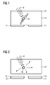
- the FIG. 1 shows an X-ray detector for direct X-ray conversion according to the known prior art.
- a material 13 suitable for absorption and direct conversion of X-ray X is disposed between a pixel electrode 11 and a top electrode 12.
- the pixelation of the electrode 11 is made for spatial resolution.
- the top electrode 12 is transparent to X-rays X.
- the X-ray X is absorbed in the material 13 to form electron-hole pairs.
- the conversion center 16 is shown, in which the conversion of the radiation energy of the X-ray X into electrical energy takes place, in which the energy of the radiation passes to an electron and this in a higher energetic Condition is lifted.
- the electron-hole pair thus formed can be separated in an applied field which can be applied to the material layer 13 via the electrodes 11, 12. That is, the X-ray detector is in operation under a bias voltage and upon absorption of X-radiation X, a current flow I can be detected.
- FIG. 2 shows an X-ray detector for indirect X-ray conversion according to the prior art.
- This X-ray detector for indirect X-ray conversion is constructed in two parts.
- the X-ray detector comprises a scintillation layer 14 in which the conversion of X-radiation X into fluorescence radiation takes place.
- a conversion center 16 is shown schematically, in which the conversion of the energy of the X-ray radiation into light energy passes.
- the second part of the X-ray detector comprises photodetectors 15, in particular photodiodes 15, and in turn pixelated electrodes 11. These photodiodes 15 are suitable for detecting the fluorescence radiation of the scintillator layer 14.
- Known scintillator materials which can be used for a scintillator layer are e.g. Gadolinium sulfur oxide or cesium iodide.
- the layer thickness of such a scintillation layer is 0.1 mm to 1 mm.
- the direct X-ray conversion layer 13 may be a silicon photodiode having a high layer thickness of more than 1 cm, or amorphous selenium may be used as a direct X-ray converter.
- the selenium layers for direct x-ray conversion are usually up to 1 mm thick.
- the direct x-ray converters are used e.g. biased in the reverse direction with voltages in the range of a few kV.
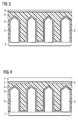
- FIGS. 3, 4 and 5 each show an X-ray detector with a hybrid photoactive layer, wherein the scintillators 2 scintillator needles, which are grown on a substrate 1.
- the scintillator needles 2 are, for example, cesium iodide scintillators.
- the substrate 1 may be a glass substrate be.
- An ALD layer 3 is deposited over the scintillator needles 2 grown on the glass substrate 1.
- the ALD layer 3 is a transparent conductive oxide (TCO). This ALD layer 3 can thus fulfill the function of the anode of the hybrid photodiode.
- TCO transparent conductive oxide
- the interstices of the scintillator needles 2 on the substrate 1 are filled with a bulk heterojunction 4 and the needles 2 are covered therewith, so that a thick hybrid photoactive layer is formed in which the scintillator needles 2 are completely embedded.
- the hybrid photoactive layer is covered by a cathode 5.
- This can in turn be applied by an ALD process.
- aluminum is used for this purpose.
- the cathode 5 can also be made by thermal evaporation of one or more metals. In FIG. 3 the cathode 5 is applied over a large area to the photoactive layer.
- the application of the anode 3 by an ALD process to the scintillator needles 2 has the advantage that an isotropic deposition takes place even with a high aspect ratio of the scintillator needle 2.
- FIG. 4 Also shown is a substrate 1 with raised scintillator needles 2 covered by an ALD layer 3. Again, the deposition of a bulk heterojunction 4 occurs in the needle interstices and on the scintillator needles 2 so that they are completely embedded in the bulk heterojunction 4 and form a hybrid photoactive layer with the bulk heterojunction 4.
- the top electrode 5, which represents the cathode of the hybrid photodiode, is shown pixelated in this case, ie, the cathode 5 is interrupted and it can thus be a spatial resolution. Above the cathode 5, a further substrate 1 is shown. This can be part of an encapsulation of the X-ray detector.
- the hybrid photoactive layer may be completely encapsulated to protect it against the ingress of moisture which could adversely affect the organic materials and also adversely affect hygroscopic scintillator material.
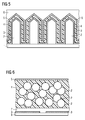
- FIG. 5 shows an alternative embodiment of the X-ray detector in which the scintillator needles 2 are grown back on a substrate 1 and both electrodes 3, 5 were deposited isotropically by ALD process.
- the anode 3 is deposited directly on the scintillator needles 2.
- the cathode 5 is deposited on the bulk heterojunction 4.
- the bulk heterojunction 4 is deposited in this case only as a relatively thin layer over the needles 2. In particular, the bulk heterojunction 4 is less than 100 nm in layer thickness.
- the electrode layers 3,5 and the bulk heterojunction 4 thus still form the needle structure.
- the interspinous spaces are then filled with a filling material 6 and the scintillator tips covered with it.
- filler 6 for example, an epoxide can be used. This serves primarily for stabilization and moisture protection of the hybrid photodetector.
- the anode 3 is always arranged between the scintillators 2 and the bulk heterojunction 4.
- the scintillation radiation In order for the scintillation radiation, which is excited in the scintillators 2 by the penetrating X-ray radiation X, to be absorbed by the bulk heterojunction 4, the scintillation radiation must be able to exit through the anode 3 into the bulk heterojunction 4.
- a transparent conductive oxide (TCO) is used as the anode 3. This can be deposited in particular by an ALD process. The transparency must be ensured, above all, in the wavelength range in which the scintillators 2 emit radiation. In this case, an isotropic emission can take place in the photoactive organic semiconductor material 4.
- the X-ray detector can be used for dose rate measurement.
- pixelated electrodes 3, 5 are used, in this case preferably a pixelated cathode 5, as in FIG. 4 shown.
- Particularly advantageous for this purpose is an ALD-deposited anode 3 which has a refractive index which causes the scintillation radiation to be totally reflected at the surface of the scintillators 2 and conducted in the scintillator needles 2 as in an optical waveguide. Then, if an interruption of the ALD layer, preferably provided at the needle tips, the fluorescence radiation occurs bundled at this point and ensures a high spatial resolution of the X-ray detector.
- the FIG. 6 1 shows a hybrid photodiode with embedded scintillator particles 2 in the bulk heterojunction 4.
- This hybrid photoactive layer is arranged between a cathode 5 and a substrate 8 with pixelated anodes 3. Between the pixelated anodes 3 and the hybrid photoactive layer may still be an intermediate layer 7. In general, intermediate layers 7 or so-called interlayer 7 can be used to promote charge transport to the electrodes 3, 5.
- the substrate 8 is in this case an active matrix backplane, via which the pixel anodes 3 can be controlled and read out.
- the conversion of X-radiation X into fluorescence radiation takes place in the scintillators 2.
- the fluorescence radiation is absorbed in the bulk heterojunction 4 and converted into electrical energy.
- the electron-hole pairs generated by the absorption of the fluorescence radiation are as well as in FIG. 1 shown separated in the applied field between anode 3 and cathode 5 and detected.
- an isotropic emission of the fluorescence radiation into the bulk heterojunction 4 takes place. This causes an efficient conversion of the X-ray energy into electrical signals.
- the layer thickness of the hybrid photoactive layer with the bulk heterojunction 4 and the embedded scintillators 2 is about 100 microns, but may also be only 10 microns, depending on the application. For example, very thin layer thicknesses of the hybrid photoactive layer of about 1 ⁇ m are possible.
- the structuring of the electrodes 3, 5 determines the active area of the hybrid photodiodes.
- the pixelation of the electrodes 3, 5, depending on whether on the substrate 1, 8 or on the bulk heterojunction 4, can preferably take place via shadow masks or lithographically.
- the structuring by shadow masks is advantageous in a direct Aufdampfvorgang the top electrode.
- the pixel pitch is preferably 50 ⁇ m.
- the active diode area is chosen to be very large, especially for dose rate measurements, and can be up to 10 cm 2 .
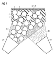
- FIG. 7 now shows schematically the manufacturing process of a hybrid photodetector with particulate scintillators 2.
- the hybrid photoactive layer is applied in a co-spraying. That is, the bulk heterojunction (BHJ) 4 is sprayed from a solution 40 simultaneously with a suspension 20 containing the scintillator particles 2.
- BHJ bulk heterojunction
- two spray heads 21, 41 are shown, which are aligned on the same substrate 3, 7, 8.
- the layer thickness of the hybrid photoactive layer can be adjusted in a targeted manner.
- the sprayed layer thicknesses are between 0.5 and 100 microns.
- Advantageous proportions of scintillator particles 2 in the bulk heterojunction 4 are between 10% by volume and 50% by volume.
- the scintillator is discretely applied to the substrate in this co-spraying process.
- FIGS. 8, 9 and 10 show sensors with a dimension of 43 x 43 cm, as they can be used in existing X-ray equipment for dose rate measurement of the so-called Automatic Exposure Control (AEC).
- AEC Automatic Exposure Control
- the three-field arrangement, as in FIG. 8 shown covers the lung and mediastinal area, as it is important in medical applications of x-ray equipment.
- the hatched areas 80, 90 in the FIGS. 8 and 9 represent the sensor surfaces.
- an inventive arrangement of sensor surfaces 100 is shown, as they can be particularly well realized by the X-ray detectors according to the invention with hybrid photoactive layer. These are very thin and can be separated over a large area.
- a kind of checkerboard pattern that is, an arrangement of the sensors 100 in a two-dimensional 5x5 matrix done.
- a sensor with several, eg 13 sensor fields 100, it is possible to react very flexibly to objects to be examined differently.
- Various combinations of the sensor fields 100 can be actively switched and used.
- the sensor fields 100 for dose rate measurement must not cast shadows on the X-ray image.
- the FIG. 11 shows an X-ray device 70 as used for the examination of an examination subject 700, for example in medicine.
- the examination object 700 is attached above the x-ray detector unit 73, 74.
- This consists of an X-ray detector for dose rate measurement 73 and an X-ray detector for the imaging 74.
- an X-ray detector for dose rate measurement can also be attached above the examination subject 700.
- the X-ray tube 72 in which the X-ray X is generated, is arranged so that the X-ray X penetrates the examination subject 700 and then hits the X-ray detector unit 73, 74.
- a driver 71 of the X-ray tube 72 is shown.
- This image of an X-ray machine shows that two X-ray detectors 73, 74 with very different requirements for the X-ray measurement are necessary.
- it has hitherto been necessary to apply very different technologies for X-ray imaging e.g. via indirect converters and for X-ray dose rate measurement e.g. recourse to ionization chambers.
- an X-ray detector for dose rate measurement as well as for imaging can be produced.
- the dose rate measurement it is advantageous for the dose rate measurement to have a low component depth in order to absorb as little X-radiation as possible, since this is still intended to impinge on the imaging in the second X-ray detector 74 for imaging.
- the efficient conversion of the energy of the X-radiation X into signal charges is of particular importance.
- the highest possible radiation should be absorbed. It is always about a trade-off between absorption and actual performance. That the quantum efficiency and the dynamic behavior of the X-ray diode deteriorate with increasing layer thickness.
- the absorption of the X-ray X in the hybrid photoactive layer increases exponentially with the layer thickness.
- the absorption should be low.
- layer thicknesses between 5 and 20 microns and a Szintillatoranteil of 50 vol .-% of advantage For X-ray imaging, layer thicknesses between 100 ⁇ m and 1 mm are preferably used.
- scintillator needles 2 with an ALD layer jacket 3 are advantageous, by which the scintillator needles 2 function as optical waveguides.
- the FIG. 12 shows a diagram in which the efficiency of the conversion of the different X-ray detectors is shown.
- the measurement results A and C are each assigned to an X-ray detector based on indirect conversion, the measurement results B an X-ray detector based on direct conversion.
- the measured current I n which was normalized to the dose rate and to the layer thickness of the respective X-ray detector.
- the current is indicated in amperes.
- the dose rate in micro-gray per second ( ⁇ Gr / s).
- an organic X-ray detector based on a bulk heterojunction with embedded lead-selenium quantum dots was used as an X-ray detector based on direct conversion. Its measurement results are marked B in the diagram.
- the quantum dots account for 50% by volume of the conversion layer.
- the embedding of quantum dots, so-called quantum dots, in an organic semiconductor material is based on direct X-ray conversion in the quantum dots, wherein the organic semiconductor material is responsible for the removal of the generated electrical charge.
- the measurement points labeled A are a prior art two-piece x-ray detector as in FIG FIG. 2 shown, assign. In this case, organic photodiodes were used as the photodetector and a 1 mm thick cesium iodide scintillator.
- the measurement designated C is assigned to a hybrid X-ray detector according to the invention comprising a hybrid photoactive layer of a bulk heterojunction 4 and embedded scintillator particles 2 of gadolinium sulfur oxide. These were deposited by the co-spraying process according to the invention.
- the hybrid photoactive layer is 10 ⁇ m.
- the gadolinium sulfur oxide particles account for 50% by volume of the active layer.
- the conversion efficiency can be tuned over the layer thickness.
- the evaluation of the various X-ray detectors takes place at a known dose rate ( ⁇ G / s).
- a difference between the embedded quantum dots and the scintillator particles 2 is in the size of the particles.
- the scintillator particles 2 are between 1 .mu.m and 4 .mu.m in diameter.
- the quantum dots range in diameter between 3 nm and 6 nm. Therefore, the conversion principle differs.
- the X-rays are converted directly into electrical charge and the organic Semiconductor material serves as a carrier for the quantum dots and as a conductive material for the removal of the charge.
- the scintillator particles the X-radiation is converted into scintillating radiation, which lies in particular in visible light, and is converted into charge via an organic photoactive material.
Abstract
Description
Die vorliegende Erfindung betrifft Röntgendetektoren auf Basis indirekter Röntgenkonversion.The present invention relates to X-ray detectors based on indirect X-ray conversion.
Im Bereich der Röntgendetektoren wird grundsätzlich danach unterschieden, ob der Röntgendetektor auf direkter oder auf indirekter Röntgenkonversion basiert. Beide Formen der Röntgendetektion sind in den
Bei der direkten Röntgenkonversion wird die Röntgenstrahlung in einem Material absorbiert und mit deren Energie ein Elektron-Loch-Paar erzeugt. Das erzeugte Elektron-Loch-Paar kann elektronisch ausgelesen werden. Als Material kommt dafür beispielsweise amorphes Selen zum Einsatz. Auch Siliziumdioden werden zur direkten Röntgenkonversion verwendet. Bei der direkten Röntgenkonversion in einem Halbleiter kommt es auf eine gewisse Schichtdicke an, um einen für eine Detektion ausreichend hohen Anteil der Strahlung zu absorbieren. Siliziumdioden für die direkte Röntgenkonversion weisen Bauteildicken von ungefähr 1 cm auf. Für direkte Röntgenkonversion in amorphem Selen werden Schichten von bis zu 1 mm Dicke verwendet. Besonders nachteilig an Selen als Absorber ist dessen hohe Toxizität.In direct X-ray conversion, the X-rays are absorbed in a material and their energy creates an electron-hole pair. The generated electron-hole pair can be read out electronically. As a material, for example, amorphous selenium is used. Silicon diodes are also used for direct X-ray conversion. In the case of direct X-ray conversion in a semiconductor, a certain layer thickness is important in order to absorb a sufficiently high proportion of the radiation for detection. Silicon diodes for direct X-ray conversion have component thicknesses of approximately 1 cm. For direct X-ray conversion in amorphous selenium, layers up to 1 mm thick are used. A particular disadvantage of selenium as an absorber is its high toxicity.
Für die indirekte Röntgenkonversion kommen bekannterweise Kombinationen aus einer Szintillatorschicht und einem Fotodetektor zum Einsatz. Dabei liegt die spektrale Empfindlichkeit des Fotodetektors in dem Wellenlängenbereich der Fluoreszenzemission der Szintillatorschicht, die durch Röntgenkonversion erzeugt wird. Die Szintillatorschichten umfassen Materialien wie z.B. Cäsiumjodid oder Gadoliniumschwefeloxid. Da Szintillatoren aus Cäsiumjodid höchst hygroskopisch sind, ist deren Einsatz in Kombination mit Fotodetektoren stets mit baulichem Aufwand, z.B. für eine Feuchteschutzverkapselung, verbunden und nachteilig für die Lebensdauer des Röntgendetektors. Neben den beiden grundsätzlich möglichen Röntgenkonversionsformen muss im Bereich der Röntgendetektion auch nach dem Einsatzfeld unterschieden werden. Im Einsatzfeld der Röntgenbildgebung, wie sie beispielsweise im Medizinbereich Einsatz findet, werden kostengünstige und großflächige Lösungen angestrebt. Dabei kommt es auf eine hohe örtliche Auflösung für die Bildgebung an. Dafür werden bisher entweder direkte Röntgenkonverter eingesetzt, die jedoch nachteilig mit hohen Bauteiltiefen aufwarten und daher energetisch ineffizient hohe Betriebsspannungen im kV-Bereich benötigen. Oder es kommt eine Szintillatorschicht auf einem Fotodetektorarray zum Einsatz, welches nachteilig aus einer Vielzahl an pixelierten Fotodetektoren aufgebaut sein muss, um die gewünschte örtliche Auflösung zu gewährleisten.As is known, combinations of a scintillator layer and a photodetector are used for indirect X-ray conversion. The spectral sensitivity of the photodetector lies in the wavelength range of the fluorescence emission of the scintillator layer, which is produced by X-ray conversion. The scintillator layers include materials such as cesium iodide or gadolinium sulfur oxide. Since cesium iodide scintillators are highly hygroscopic, their use in combination with photodetectors is always constructional Effort, eg for a moisture protection encapsulation, connected and disadvantageous for the life of the X-ray detector. In addition to the two basically possible X-ray conversion forms, a distinction must also be made according to the field of use in the area of X-ray detection. In the field of X-ray imaging, as used for example in the field of medicine, cost-effective and large-scale solutions are sought. It all depends on a high spatial resolution for the imaging. For this purpose, either direct X-ray converters have been used up to now, but these disadvantageously come up with high component depths and therefore require energetically inefficiently high operating voltages in the kV range. Or, a scintillator layer is used on a photodetector array, which must be disadvantageously constructed from a plurality of pixelated photodetectors to ensure the desired spatial resolution.
Daneben finden Röntgendetektoren in der Röntgendosisleistungsmessung Einsatz. Die Röntgendosis wird in Röntgengeräten im medizinischen Bereich überwacht sowie auch in der Industrie und Sicherheitstechnik in sogenannten Dosimetern gemessen. Für die Röntgendosismessung ist eine effiziente Wandlung der absorbierten Röntgenstrahlung in ein nutzbares Signal von Bedeutung. Die Signale sollen ausreichend hoch und rauschfrei sein, um eine genaue Röntgendosis zu bestimmen. Insbesondere für den Einsatz von Röntgendosiskontrollgeräten in Kombination mit einer Röntgenbildgebung ist eine geringe Absorption der Röntgenstrahlung von Bedeutung. D.h. aus nur wenig absorbierter Röntgenstrahlung muss ein eindeutiges Signal generiert werden. Dies ist notwendig um keine Schatten auf dem Röntgenbild zu erzeugen. Besonders aber ist die geringe Absorption bei der Dosismessung nötig, um für ein deutliches Röntgenbild die Röntgenbelastung, beispielsweise für einen Patienten, möglichst gering zu halten. Bisher kommen zur Kontrolle der Röntgendosisleistung Ionisationskammern oder beispielsweise dicke Siliziumfotodioden zum Einsatz.In addition, X-ray detectors are used in the X-ray dose rate measurement. The X-ray dose is monitored in X-ray machines in the medical field and also measured in industry and safety technology in so-called dosimeters. For X-ray dose measurement, efficient conversion of the absorbed X-ray radiation into a usable signal is important. The signals should be sufficiently high and noise free to determine an accurate X-ray dose. In particular, for the use of X-ray dose control devices in combination with X-ray imaging is a low absorption of X-rays of importance. This means that only a small amount of absorbed X-rays require a clear signal. This is necessary to avoid shadows on the X-ray image. In particular, however, the low absorption in the dose measurement is necessary in order to keep the X-ray exposure, for example for a patient, as low as possible for a clear X-ray image. So far, ionization chambers or, for example, thick silicon photodiodes are used to control the X-ray dose rate.
Nachteilig an den bisher bekannten Röntgendetektoren ist, dass diese für einen jeweils stark eingeschränkten Nutzungsbereich geeignet sind. Die unterschiedlichen Funktionsweisen zur Röntgendetektion sind nicht vorteilhaft miteinander kombinierbar. Außerdem weisen alle bisher bekannten Röntgendetektoren hohe Bauteiltiefen auf.A disadvantage of the previously known X-ray detectors that they are suitable for a severely limited range of use. The different modes of operation for X-ray detection can not be advantageously combined. In addition, all previously known X-ray detectors on high component depths.
Es ist Aufgabe der vorliegenden Erfindung, einen Röntgendetektor bereitzustellen, der gleichermaßen zur Röntgenbildgebung sowie auch zur Röntgendosismessung herangezogen werden kann. Darüber hinaus ist es eine Aufgabe der vorliegenden Erfindung eine Anordnung dieses Röntgendetektors mit einem Röntgengerät bereitzustellen, sowie ein Verfahren zu dessen Herstellung anzugeben.It is an object of the present invention to provide an X-ray detector which can be used equally for X-ray imaging as well as X-ray dose measurement. Moreover, it is an object of the present invention to provide an arrangement of this X-ray detector with an X-ray apparatus, and to provide a method for its production.
Die Aufgabe wird gelöst durch einen Röntgendetektor gemäß Anspruch 1 und durch eine Anordnung des Röntgendetektors mit einem Röntgengerät gemäß Anspruch 8, sowie durch ein Verfahren gemäß Anspruch 11. Vorteilhafte Ausgestaltungen der Erfindung sind Gegenstand der Unteransprüche.The object is achieved by an X-ray detector according to
Der erfindungsgemäße Röntgendetektor ist für die Bildgebung und/oder für die Dosisleistungsmessung ausgestaltet. Der Röntgendetektor umfasst eine hybride fotoaktive Schicht zwischen einer ersten Elektrode und einem Substrat. Die erste Elektrode ist insbesondere die Kathode der Fotodiode. Die hybride fotoaktive Schicht umfasst eine Mehrzahl an Szintillatoren sowie eine Bulk-Heterojunction. Die fotoaktive Schicht wird als hybrid bezeichnet, da sie mit den Szintillatoren und der Bulk-Heterojunction zwei unterschiedliche Konvertermaterialien umfasst. Diese sind jedoch nicht wie bisher bekannt in getrennten Schichten angeordnet, sondern zu einer einzelnen fotoaktiven Schicht verbunden. Die Szintillatoren dienen zur Konversion der Röntgenstrahlung in Szintillationsstrahlung, insbesondere Fluoreszenzstrahlung im sichtbaren Wellenlängenbereich. Die Bulk-Heterojunction ist ausgestaltet in eben diesem Wellenlängenbereich der Szintillationsstrahlung zu absorbieren und dadurch Elektron-Loch-Paare zu bilden. Die hybride fotoaktive Schicht, die Szintillatoren und eine Bulk-Heterojunction aufweist, ist daher ausgestaltet indirekte Röntgenkonversion vorzunehmen. Der Röntgendetektor ist darüber hinaus so ausgestaltet, die Elektron-Loch-Paare, die in der Bulk-Heterojunction generiert werden, elektrisch zu detektieren. Der erfindungsgemäße Röntgendetektor hat den Vorteil mit einer einzelnen hybriden fotoaktiven Schicht zwischen einer ersten Elektrode und einem Substrat mit einer geringen Bauteiltiefe auszukommen, sowie einen sehr einfachen Aufbau aufzuweisen. Der erfindungsgemäße Röntgendetektor kommt darüber hinaus ohne hochtoxisches Selen aus. Die hybride fotoaktive Schicht ist gleichermaßen geeignet eine Bildgebung oder eine Dosisleistungsmessung zu gewährleisten.The X-ray detector according to the invention is designed for imaging and / or for dose rate measurement. The X-ray detector comprises a hybrid photoactive layer between a first electrode and a substrate. The first electrode is in particular the cathode of the photodiode. The hybrid photoactive layer comprises a plurality of scintillators as well as a bulk heterojunction. The photoactive layer is referred to as hybrid because it comprises two different converter materials with the scintillators and the bulk heterojunction. However, these are not arranged as previously known in separate layers, but connected to a single photoactive layer. The scintillators serve to convert the X-ray radiation into scintillation radiation, in particular fluorescence radiation in the visible wavelength range. The bulk heterojunction is designed to absorb the scintillation radiation in precisely this wavelength range and thereby form electron-hole pairs. The hybrid photoactive layer, which has scintillators and a bulk heterojunction, is therefore designed to perform indirect X-ray conversion. The X-ray detector is further configured to electrically detect the electron-hole pairs generated in the bulk heterojunction. The X-ray detector according to the invention has the advantage of having a single hybrid photoactive layer between a first electrode and a substrate with a small component depth, and having a very simple structure. In addition, the X-ray detector according to the invention does not require highly toxic selenium. The hybrid photoactive layer is equally suitable for ensuring imaging or dose rate measurement.
Als Bulk-Heterojunction werden in der organischen Elektronik Heteroübergänge bezeichnet, die sich über das gesamte Schichtvolumen (bulk) erstrecken. Mindestens zwei Materialien, die sich in ihrer Eigenschaft als Loch- oder Elektronleiter unterscheiden (hetero), werden so zu einer Schicht zusammengefügt, dass sich im gesamten Schichtvolumen Grenzflächen der beiden Materialien ausbilden. In einer Bulk-Heterojunction erfolgt die Trennung der Ladungsträger, d.h. der Elektron-Loch-Paare, an eben diesen Grenzflächen.Holo heterojunction is used in organic electronics to refer to heterojunctions that extend over the entire layer volume (bulk). At least two materials, which differ in their capacity as hole or electron conductors (hetero), are combined to form a layer that forms interfaces of the two materials in the entire layer volume. In a bulk heterojunction, the separation of the charge carriers, i. the electron-hole pairs, at just these interfaces.
In einer vorteilhaften Ausgestaltung der Erfindung umfasst die Bulk-Heterojunction organische Halbleitermaterialien, die löslich sind und durch einen Sprühprozess abscheidbar sind. Diese Eigenschaften sind vorteilhaft für die Absorptionseigenschaft sowie die Eignung zur Trennung von Elektron-Loch-Paaren in der Bulk-Heterojunction, denn nur bei Eignung für eine bestimmte Abscheidetechnik sind effiziente Bulk-Heterojunctions herstellbar.In an advantageous embodiment of the invention, the bulk heterojunction comprises organic semiconductor materials which are soluble and can be deposited by a spraying process. These properties are advantageous for the absorption property as well as the suitability for the separation of electron-hole pairs in the bulk heterojunction, because efficient bulk heterojunctions can only be produced if they are suitable for a specific deposition technique.
In einer weiteren vorteilhaften Ausgestaltung der Erfindung machen die Szintillatoren einen Volumenanteil zwischen 10 Vol.-% und 70 Vol.-% der hybriden fotoaktiven Schicht aus, insbesondere zwischen 10 Vol.-% und 50 Vol.-%. Ein derartiger Volumenanteil an Szintillatoren in der hybriden fotoaktiven Schicht wirkt sich positiv auf die energetische Umsetzung der Röntgenstrahlung in elektrische Signale aus. Insbesondere kann in diesem Intervall eine Anpassung vorgenommen werden für einen Einsatz zur Dosismessung oder zur Bildgebung. Für die Dosismessung ist eine geringere Absorption, für die Bildgebung eine höhere Absorption der Röntgenstrahlung vorteilhaft.In a further advantageous embodiment of the invention, the scintillators make up a volume fraction of between 10% by volume and 70% by volume of the hybrid photoactive layer, in particular between 10% by volume and 50% by volume. Such a volume fraction of scintillators in the hybrid photoactive Layer has a positive effect on the energetic conversion of the X-radiation into electrical signals. In particular, an adjustment can be made in this interval for use for dose measurement or imaging. For the dose measurement is a lower absorption, for imaging a higher absorption of the X-radiation advantageous.
In einer weiteren vorteilhaften Ausgestaltung der Erfindung weist die hybride fotoaktive Schicht eine homogene Schichtdicke auf, und diese Schichtdicke beträgt zwischen 0,5 µm und 500 µm, insbesondere zwischen 0,5 µm und 100 µm. Die Gesamtschichtdicke der hybriden fotoaktiven Schicht beträgt insbesondere 500 µm. Die Gesamtschichtdicke der hybriden fotoaktiven Schicht kann auch 100 µm oder nur 10 µm betragen. Auch Gesamtschichtdicken von 1 µm sind realisierbar. Die dünne Schichtdicke wirkt sich dementsprechend auf die gesamte Bauteildicke vorteilhaft aus. Insbesondere kann durch eine Variation der Schichtdicke der hybriden fotoaktiven Schicht der Röntgendetektor auf den Einsatz zur Dosisleistungsmessung mit einer dünneren hybriden fotoaktiven Schicht oder für den Einsatz zur Röntgenbildgebung mit einer dickeren hybriden fotoaktiven Schicht ausgestaltet werden.In a further advantageous embodiment of the invention, the hybrid photoactive layer has a homogeneous layer thickness, and this layer thickness is between 0.5 .mu.m and 500 .mu.m, in particular between 0.5 .mu.m and 100 .mu.m. The total layer thickness of the hybrid photoactive layer is in particular 500 μm. The total layer thickness of the hybrid photoactive layer may also be 100 μm or only 10 μm. It is also possible to achieve total layer thicknesses of 1 μm. The thin layer thickness accordingly has an advantageous effect on the entire component thickness. In particular, by varying the layer thickness of the hybrid photoactive layer, the X-ray detector can be configured for use for dose rate measurement with a thinner hybrid photoactive layer or for use for X-ray imaging with a thicker hybrid photoactive layer.
In einer weiteren vorteilhaften Ausgestaltung der Erfindung weist der Röntgendetektor eine ALD-Schicht auf. Insbesondere ist die ALD-Schicht eine zweite Elektrode des Röntgendetektors. Die zweite Elektrode ist insbesondere die Anode der Fotodiode.In a further advantageous embodiment of the invention, the X-ray detector has an ALD layer. In particular, the ALD layer is a second electrode of the X-ray detector. The second electrode is in particular the anode of the photodiode.
Als ALD-Schicht wird eine Schicht bezeichnet, die durch einen ALD-Prozess hergestellt wurde. ALD steht für Atomic Layer Deposition, ein bekanntes Abscheideverfahren. Mittels ALD können Schichten mit charakteristischen Eigenschaften erzeugt werden. Eine ALD-Schicht ist insbesondere auf eine Atomlage in ihrer Dicke homogen. Insbesondere ist eine ALD-Schicht isotrop bezüglich ihrer elektrischen, optischen oder mechanischen Eigenschaften.The ALD layer refers to a layer produced by an ALD process. ALD stands for Atomic Layer Deposition, a well-known separation method. ALD can be used to create layers with characteristic properties. An ALD layer is particularly homogeneous in thickness to an atomic layer. In particular, an ALD layer is isotropic with respect to its electrical, optical or mechanical properties.
Der Einsatz einer ALD-Schicht als zweiter Elektrode ist besonders vorteilhaft da die ALD-Schicht gleichermaßen als feuchte Schutzschicht dienen kann und somit eine Verkapselung zum Feuchteschutz ersetzt oder dieser durch die ALD-Schicht unterstützt werden kann.The use of an ALD layer as a second electrode is particularly advantageous since the ALD layer can equally serve as a moist protective layer and thus replaces an encapsulation for moisture protection or this can be supported by the ALD layer.
Insbesondere ist die ALD-Schicht zwischen den Szintillatoren und der Bulk-Heterojunction angeordnet. Beispielsweise sind dazu Szintillatornadeln oder Szintillatorpartikel in einem ALD-Prozess beschichtet worden, bevor die Bulk-Heterojunction darauf abgeschieden wurde. In diesem Aufbau wirkt die ALD-Schicht besonders effektiv als Feuchtigkeitsbarriere um die Szintillatoren herum.In particular, the ALD layer is disposed between the scintillators and the bulk heterojunction. For example, scintillator needles or scintillator particles have been coated in an ALD process before the bulk heterojunction has been deposited thereon. In this construction, the ALD layer is particularly effective as a moisture barrier around the scintillators.
Das Einbringen einer ALD-Schicht als eine der Elektroden, insbesondere als Anode, hat also den zusätzlichen Vorteil, dass die davon umgebenen Szintillatoren einen Feuchteschutz erfahren. Die dichte ALD-Schicht vermindert die Feuchteaufnahme der hybriden fotoaktiven Schicht und wirkt wie eine Verkapselung. Zusätzlich kann um das gesamte Bauteil mit hybrider fotoaktiver Schicht Substrat und Elektroden herum eine weitere Verkapselung vorgenommen werden. Hierfür ist insbesondere eine Dünnfilmverkapselung von Vorteil. Die hybride Ausgestaltung des Röntgendetektors bietet damit den Vorteil, dass keine getrennte Verkapselung von organischer fotoaktiver Schicht und Szintillatorschicht notwendig ist. Reaktive Top-Elektroden, die z.B. Kalzium enthalten, können insbesondere durch ALD abgeschiedene Aluminium-Top-Elektroden ersetzt werden. Somit können sehr langzeitstabile Röntgendetektoren geschaffen werden.The introduction of an ALD layer as one of the electrodes, in particular as an anode, thus has the additional advantage that the scintillators surrounded by it experience a moisture protection. The dense ALD layer reduces the moisture absorption of the hybrid photoactive layer and acts like an encapsulation. In addition, a further encapsulation can be carried out around the entire component with a hybrid photoactive layer substrate and electrodes. For this purpose, in particular a thin-film encapsulation is advantageous. The hybrid design of the X-ray detector thus offers the advantage that no separate encapsulation of organic photoactive layer and scintillator layer is necessary. Reactive top electrodes, e.g. Contain calcium, in particular can be replaced by ALD deposited aluminum top electrodes. Thus, very long-term stable X-ray detectors can be created.
In einer weiteren vorteilhaften Ausgestaltung der Erfindung ist die ALD-Schicht zumindest teilweise durchlässig für elektromagnetische Strahlung im zu detektierenden Wellenlängenbereich der Röntgenstrahlung oder für Licht im Wellenlängenbereich der Szintillationsstrahlung der Szintillatoren.In a further advantageous embodiment of the invention, the ALD layer is at least partially transmissive to electromagnetic radiation in the wavelength range of the X-radiation to be detected or to light in the wavelength range of the scintillating radiation of the scintillators.
In einer weiteren vorteilhaften Ausgestaltung der Erfindung ist der Brechungsindex der ALD-Schicht genau in dem Wellenlängenbereich höher als der Brechungsindex des Szintillatormaterials, in dem die Fluoreszenzstrahlung liegt, die im Szintillator anregbar ist. Das hat den Vorteil, dass die den Szintillator treffende Röntgenstrahlung im Szintillator eine Fluoreszenzstrahlung anregt, die dann in dem Szintillator wie in einem Lichtwellenleiter an der ALD-Schicht total reflektiert wird und so zielgerichtet an einem vorgebbaren Ausgangspunkt des Lichtwellenleiters austritt. Ein derartiger Ausgangspunkt ist eine Lücke in der ALD-Schicht, die in nadelförmigen Szintillatoren vorzugsweise an der Nadelspitze angeordnet ist.In a further advantageous embodiment of the invention, the refractive index of the ALD layer is exactly higher in the wavelength range than the refractive index of the scintillator material in which the fluorescence radiation is present, which can be excited in the scintillator. This has the advantage that the X-ray radiation striking the scintillator excites fluorescence radiation in the scintillator, which is then totally reflected in the scintillator as in an optical waveguide on the ALD layer and thus exits in a targeted manner at a predefinable starting point of the optical waveguide. One such starting point is a gap in the ALD layer which is preferably located at the needle point in acicular scintillators.
In der erfindungsgemäßen Anordnung mit einem Röntgengerät weist das Röntgengerät einen Sensor auf, der ein Dreifeldoder ein Fünffeldsensor zur Kontrolle der applizierten Röntgendosis ist. Dieser Dreifeld- oder Fünffeldsensor weist wiederum erfindungsgemäße Röntgendetektoren auf. Insbesondere ist der Detektor zur Dosiskontrolle im Strahlengang der Röntgenstrahlung zwischen der Röntgenröhre, d.h. der Röntgenstrahlungsquelle, und der Bildgebungseinheit angeordnet. Eine derartige Anordnung mit einem Röntgengerät, welches zur Kontrolle der applizierten Röntgendosis einen erfindungsgemäßen Röntgendetektor verwendet, hat den Vorteil, dass der Röntgendetektor eine geringe Bauteiltiefe und geringe Absorption aufweist und dementsprechend sich der Sensor nicht nachteilig auf die Röntgenbildgebung auswirkt. Darüber hinaus gewährleistet der erfindungsgemäße Röntgendetektor eine effiziente Wandlung der absorbierten Röntgenenergie in ein detektierbares elektrisches Signal.In the arrangement according to the invention with an x-ray device, the x-ray device has a sensor which is a three-field or a five-field sensor for controlling the applied x-ray dose. This three-field or five-field sensor in turn has inventive X-ray detectors. In particular, the dose control detector is in the X-ray beam path between the X-ray tube, i. the X-ray source, and the imaging unit. Such an arrangement with an X-ray apparatus which uses an X-ray detector according to the invention for controlling the applied X-ray dose has the advantage that the X-ray detector has a low component depth and low absorption and, accordingly, the sensor does not adversely affect X-ray imaging. In addition, the X-ray detector according to the invention ensures efficient conversion of the absorbed X-ray energy into a detectable electrical signal.
In einer vorteilhaften Ausgestaltung der Erfindung umfasst die Anordnung mit dem Röntgengerät einen Sensor, der eine Mehrzahl an Röntgendetektoren aufweist, die in einer zweidimensionalen Matrixanordnung angebracht sind. Die erfindungsgemäßen Röntgendetektoren haben den Vorteil aufgrund ihrer geringen Schichtdicke und dementsprechend geringen Absorption auch für den Zweck der Dosiskontrolle großflächig aufgetragen werden zu können. Demnach ist eine sehr exakte Dosismessung möglich. Für den Anwendungsbereich der Bildgebung wirkt sich ein entsprechender Röntgendetektor ebenso vorteilhaft aus. Durch die hybride fotoaktive Schicht können Röntgensensoren großflächig hergestellt werden und beispielsweise in einer Matrix strukturiert werden um eine Ortsauflösung zu gewährleisten.In an advantageous embodiment of the invention, the arrangement with the X-ray device comprises a sensor which has a plurality of X-ray detectors which are mounted in a two-dimensional matrix arrangement. The X-ray detectors according to the invention have the advantage due to their small layer thickness and correspondingly low absorption also for the purpose of dose control can be applied over a large area. Accordingly, a very accurate dose measurement is possible. For the scope of imaging, a corresponding X-ray detector also has an advantageous effect. By the hybrid photoactive layer X-ray sensors can be produced over a large area and, for example, structured in a matrix to ensure a spatial resolution.
Insbesondere weist die Anordnung mit dem Röntgengerät einen Sensor auf, der eine Standardgröße für Automatic Exposure Control Einheiten von 43 x 43 cm2 aufweist. Dies hat den Vorteil, dass der neue erfindungsgemäße Sensor in allen herkömmlichen Röntgengeräten eingesetzt werden kann.In particular, the arrangement with the x-ray device has a sensor which has a standard size for automatic exposure control units of 43 × 43 cm 2 . This has the advantage that the new sensor according to the invention can be used in all conventional X-ray devices.
In dem Verfahren zur Herstellung eines erfindungsgemäßen Röntgendetektors wird eine Mehrzahl an Szintillatoren sowie eine Bulk-Heterojunction auf ein Substrat abgeschieden, wobei die Bulk-Heterojunction aus Lösung mittels eines Sprühprozesses abgeschieden wird. Dies hat den Vorteil, dass unterschiedliche organische Halbleitermaterialien, die nur in unterschiedlichen Lösemitteln gelöst werden können, gleichzeitig abgeschieden werden können, wodurch erst eine Bulk-Heterojunction erzeugt werden kann. Der Sprühprozess ist des Weiteren vorteilhaft für eine großflächige Abscheidung der Bulk-Heterojunction.In the method for producing an X-ray detector according to the invention, a plurality of scintillators and a bulk heterojunction are deposited on a substrate, wherein the bulk heterojunction is deposited from solution by means of a spraying process. This has the advantage that different organic semiconductor materials, which can only be dissolved in different solvents, can be deposited simultaneously, whereby only a bulk heterojunction can be generated. The spraying process is furthermore advantageous for a large-area deposition of the bulk heterojunction.
In einer vorteilhaften Ausgestaltung der Erfindung werden in dem Verfahren die Szintillatoren aus einer Suspension durch einen Sprühprozess abgeschieden. Dabei werden die Szintillatoren insbesondere durch einen Co-Sprühprozess gleichzeitig mit der Bulk-Heterojunction abgeschieden. Bei dem Co-Sprühprozess wird die Suspension mit den Szintillatoren sowie die Lösung der Bulk-Heterojunction-Materialien auf ein gemeinsames Substrat abgeschieden und somit eine erfindungsgemäße hybride fotoaktive Schicht ausgebildet. Dies hat den Vorteil, dass ein erfindungsgemäßer Röntgendetektor in einem einzelnen Depositionsschritt hergestellt werden kann.In an advantageous embodiment of the invention, the scintillators are deposited from a suspension by a spraying process in the process. The scintillators are deposited in particular by a co-spraying process simultaneously with the bulk heterojunction. In the co-spraying process, the suspension with the scintillators and the solution of the bulk heterojunction materials are deposited on a common substrate and thus a hybrid photoactive layer according to the invention is formed. This has the advantage that an inventive X-ray detector can be produced in a single deposition step.
In einer alternativen vorteilhaften Ausgestaltung der Erfindung wird in dem Verfahren die Bulk-Heterojunction aus Lösung durch einen Sprühprozess auf die bereits auf dem Substrat abgeschiedenen Szintillatoren aufgebracht. Dies hat den Vorteil, dass beispielsweise auch Szintillatoren, die nicht durch einen Sprühprozess abscheidbar sind, in erfindungsgemäßer Weise in eine Bulk-Heterojunction so einbringbar sind, dass eine hybride fotoaktive Schicht entsteht.In an alternative advantageous embodiment of the invention, in the method, the bulk heterojunction is applied from solution by a spraying process onto the scintillators already deposited on the substrate. This has the advantage that scintillators, for example, which can not be deposited by a spray process, can also be introduced into a bulk heterojunction in accordance with the invention in such a way that a hybrid photoactive layer is formed.
In einer vorteilhaften Ausgestaltung der Erfindung umfasst das Verfahren einen zusätzlichen Prozessschritt zur Abscheidung einer ALD-Schicht. D.h. nach der Abscheidung der Szintillatoren auf dem Substrat werden diese durch einen ALD-Prozess beschichtet, wobei insbesondere durch den ALD-Prozess eine Elektrode abgeschieden wird. Danach wird die Bulk-Heterojunction auf die von der ALD-Schicht beschichteten Szintillatoren abgeschieden. Dies hat den Vorteil, dass die Szintillatoren durch die ALD-Schicht eine zusätzliche Feuchteschutzschicht erhalten. Der ALD-Prozess ist dafür von Vorteil, da er eine isotrope Abscheidung auch bei schwierigen Aspektverhältnissen der zu beschichtenden Szintillatoren gewährleistet.In an advantageous embodiment of the invention, the method comprises an additional process step for depositing an ALD layer. That after the deposition of the scintillators on the substrate, they are coated by an ALD process, wherein in particular an electrode is deposited by the ALD process. Thereafter, the bulk heterojunction is deposited on the scintillators coated by the ALD layer. This has the advantage that the scintillators receive an additional moisture protection layer through the ALD layer. The ALD process is advantageous because it ensures isotropic deposition even with difficult aspect ratios of the scintillators to be coated.
Die erfindungsgemäßen Röntgendetektoren für indirekte Röntgenkonversion weisen demnach eine organische Fotodiode basierend auf einer Bulk-Heterojunction auf, in die Szintillatormaterialien eingebettet sind. Die verwendeten organischen Halbleitermaterialien für die Bulk-Heterojunction zeichnen sich dadurch aus, dass sie sehr niedrige Dunkelströme aufweisen. Im Gegensatz zu polymeren Fotoleitern, deren Leitfähigkeit unter Lichteinstrahlung erhöht werden kann, unterscheiden sich die Dunkelströme und die Ströme bei Belichtung der eingesetzten fotoaktiven Materialien um mehrere Größenordnungen. Dies ist nötig bzw. vorteilhaft für den Einsatz zur Röntgenbildgebung, um einen deutlichen Kontrast zwischen belichteten und dunklen Bereichen zu gewährleisten. Polymere Fotoleiter würden sich nicht für eine Röntgenbildgebung eignen, da hier Gradienten zwischen bestrahlten und dunklen Bereichen entstehen würden. Des Weiteren sind die eingesetzten organischen Halbleitermaterialien in dem Wellenlängenbereich der Fluoreszenzstrahlung besonders stark absorbierend, wodurch eine effektive Umsetzung der Lichtenergie in elektrische Ladung gewährleistet ist.The X-ray detectors according to the invention for indirect X-ray conversion accordingly have an organic photodiode based on a bulk heterojunction in which scintillator materials are embedded. The organic semiconductor materials used for the bulk heterojunction are characterized by having very low dark currents. In contrast to polymeric photoconductors, whose conductivity can be increased under light irradiation, the dark currents and the currents differ by several orders of magnitude when the photoactive materials used are exposed. This is necessary or advantageous for use for X-ray imaging to ensure a clear contrast between exposed and dark areas. Polymer photoconductors would not be suitable for X-ray imaging because here gradients between irradiated and dark areas would arise. Furthermore, the organic semiconductor materials used are particularly strongly absorbing in the wavelength range of the fluorescence radiation, whereby an effective conversion of the light energy into electrical charge is ensured.
Als Szintillatoren kommen dabei z.B. Cäsiumjodid oder Gadoliniumschwefeloxid in Frage. Cäsiumjodid ist ein Vertreter der nadelförmig gewachsenen Szintillatoren, die insbesondere auf einem Substrat aufgewachsen werden. Gadoliniumschwefeloxid kann partikelförmig vorliegen. Mit Szintillatornadeln können vorteilhaft Röntgendetektoren für die Röntgenbildgebung geschaffen werden. Die Szintillatorpartikel haben den Vorteil, dass deren isotrope Fluoreszenzemission im Bulk der organischen Halbleiterschicht absorbiert werden kann. Während die Partikel alternativ durch einen Sprühprozess auch ein Co-Sprühen mit der Bulklösung abscheidbar sind oder auch zeitlich vor der Abscheidung der Bulk-Heterojunction auf dem Substrat aufgebracht werden können, werden die Szintillatornadeln in jedem Fall zunächst auf dem Substrat aufgewachsen, bevor die Bulk-Heterojunction abgeschieden wird.As scintillators, e.g. Cesium iodide or gadolinium sulfur oxide in question. Cesium iodide is a representative of the needle-shaped scintillators, which are grown in particular on a substrate. Gadolinium sulfur oxide may be particulate. With scintillator needles X-ray detectors for x-ray imaging can be created advantageous. The scintillator particles have the advantage that their isotropic fluorescence emission can be absorbed in the bulk of the organic semiconductor layer. Alternatively, while the particles may also be co-sprayed with the bulk solution by a spray process, or may be applied to the substrate prior to the deposition of the bulk heterojunction, the scintillator needles are first grown on the substrate before the bulk material is deposited. Heterojunction is deposited.
Das Bauteil des Röntgendetektors, insbesondere die hybride fotoaktive Schicht aus Szintillatoren und Bulk-Heterojunction unterscheidet sich jedoch in jedem Fall dadurch von bisherigen Röntgendetektoren, dass kein Stacking, d.h. Aufeinanderschichten von Szintillatorschicht und Fotodetektionsschicht vorliegt, sondern beide Konverter in einer einzelnen Schicht enthalten sind. Insbesondere sind die Szintillatoren, ob Nadeln oder Partikel, direkt in die Bulk-Heterojunction eingebettet, so dass die Szintillatoren direkt von der Bulk-Heterojunction umgeben sind.However, in any case, the component of the X-ray detector, in particular the hybrid photoactive layer of scintillators and bulk heterojunction, differs from previous X-ray detectors in that no stacking, i. Layering of scintillator and photodetection layer is present, but both converters are contained in a single layer. In particular, the scintillators, whether needles or particles, are embedded directly in the bulk heterojunction so that the scintillators are directly surrounded by the bulk heterojunction.
Stehen die Szintillatoren nicht in direktem Kontakt mit der Bulk-Heterojunction werden sie maximal durch eine dünne ALD-Schicht von der Bulk-Heterojunction getrennt. Diese nur wenige Atomlagen dicke Schicht kann eine der Elektroden des Röntgendetektors darstellen. Insbesondere ist die Schicht auch ein Feuchtigkeitsschutz für die Szintillatoren und/oder der Organik der Bulk-Heterojunction.If the scintillators are not in direct contact with the bulk heterojunction, they are at most separated from the bulk heterojunction by a thin ALD layer. This layer, which is only a few atom layers thick, can be one of the electrodes of the X-ray detector represent. In particular, the layer is also a moisture protection for the scintillators and / or the bulk heterojunction organics.
Bei Bevorzugung einer isotropen Fluoreszenzemission aus den Szintillatoren, z.B. für die Anwendung der Dosisleistungsmessung, ist die ALD-Schicht vorzugsweise transparent im Wellenlängenbereich der Fluoreszenzstrahlung der Szintillatoren, die durch die eintreffende Röntgenstrahlung angeregt wird.In favor of an isotropic fluorescence emission from the scintillators, e.g. For the application of the dose rate measurement, the ALD layer is preferably transparent in the wavelength range of the fluorescence radiation of the scintillators, which is excited by the incident X-ray radiation.
Für den Einsatz als Röntgenbildgeber werden vorzugsweise Szintillatornadeln als Wellenleiter eingesetzt und mit einer ALD-Schicht umgeben, deren Brechungsindex so gewählt wird, dass die in den Szintillatoren entstehende Fluoreszenzstrahlung an der Oberfläche der Szintillatoren total reflektiert und in den Szintillatoren wie in einem Wellenleiter geleitet wird. Dadurch kann die Fluoreszenzstrahlung zu einem bestimmten Ausgangspunkt aus dem Szintillator geleitet werden, insbesondere zu den Nadelspitzen der Szintillatoren. Diese sind dazu nicht von einer ALD-Schicht bedeckt. Bei einem derartigen Aufbau der hybriden fotoaktiven Schicht wird nicht die gesamte Bulk-Heterojunction von Fluoreszenzstrahlung erfasst, sondern überwiegend der fotoaktive Bereich zwischen den Szintillatorspitzen und der Kathode. Dazu ist vorteilhafterweise ein Mindestabstand zwischen den Szintillatoren und der Kathode zwischen 50 und 200 nm gewählt. Derartige hybride fotoaktive Schichten gewährleisten eine effiziente Umsetzung von Röntgenstrahlung in elektrische Signalladungen bei sehr hoher örtlicher Auflösung.For use as x-ray imagers scintillator needles are preferably used as waveguides and surrounded with an ALD layer whose refractive index is chosen so that the fluorescence radiation produced in the scintillators is totally reflected on the surface of the scintillators and guided in the scintillators as in a waveguide. As a result, the fluorescence radiation can be conducted to a specific starting point from the scintillator, in particular to the needle tips of the scintillators. These are not covered by an ALD layer. In such a construction of the hybrid photoactive layer, not the entire bulk heterojunction of fluorescence radiation is detected, but predominantly the photoactive area between the scintillator tips and the cathode. For this purpose, a minimum distance between the scintillators and the cathode between 50 and 200 nm is advantageously selected. Such hybrid photoactive layers ensure efficient conversion of X-radiation into electrical signal charges at very high local resolution.
Der Röntgendetektor umfasst also neben der hybriden fotoaktiven Schicht zumindest eine erste Elektrode und ein Substrat. Das Substrat kann insbesondere ein transparentes Substrat, z.B. ein Glassubstrat sein oder auch eine Aktiv-Matrix-Backplane. Auf dem Substrat kann eine zweite Elektrode, z.B. die Anode des Fotodetektors aufgebracht sein. Die Anode kann wiederum transparent z.B. ein TCO, ein transparentes leitfähiges Oxid sein, das beispielsweise über einen ALD-Prozess abgeschieden werden kann. Die Anode kann mehrere Anodenpixel umfassen oder durchgängig sein. Zweckdienlicherweise ist eine der Elektroden die Anode oder die Kathode aus mehreren Pixeln. Beispielsweise kann für den Fall der eingebetteten Szintillatorpartikel die hybride fotoaktive Schicht zwischen der Anode und der Kathode angeordnet sein. Es können auch zwischen Anode und Kathode noch Interlayer angeordnet sein, die beispielsweise der Ladungstrennung dienen. Die Anode kann aber auch zwischen den Szintillatoren und der Bulk-Heterojunction angeordnet sein, wenn diese z.B. in Form einer ALD-Schicht über die Szintillatornadeln aufgetragen wurde. Dementsprechend ist dann nicht die Anode pixeliert, sondern die Kathode. Generell ist auch ein inverser Aufbau möglich, dass auf das Substrat zunächst die Kathode aufgebracht wird und auf die hybride fotoaktive Schicht die Anode aufgebracht wird. Vorteilhaft ist jedoch der Aufbau mit einer Top-Kathode, die beispielsweise aus einem Metall sein kann. Dafür kommen Aluminium, Kalzium-Silber- oder Kalzium-Gold-Elektroden in Frage. Derartige Metallelektroden können beispielsweise durch Verdampfungsprozesse abgeschieden werden. Bei thermischen Verdampfungsprozessen kann durch Schattenmasken eine Strukturierung der Top-Elektrode vorgenommen werden. Alternativ kann die Top-Elektrode auch durch einen ALD-Prozess isotrop aufgetragen werden, was beispielsweise mit Aluminium möglich ist. Für eine Strukturierung der Anode auf dem Substrat kann auch ein Lithographieprozess herangezogen werden. Das Substrat für die hybride fotoaktive Schicht kann insbesondere auch flexibel ausgestaltet sein.The X-ray detector thus comprises at least a first electrode and a substrate in addition to the hybrid photoactive layer. The substrate may in particular be a transparent substrate, for example a glass substrate or else an active matrix backplane. A second electrode, for example the anode of the photodetector, can be applied to the substrate. The anode may in turn be transparent, for example a TCO, a transparent conductive oxide, for example via an ALD process can be deposited. The anode may include multiple anode pixels or be continuous. Conveniently, one of the electrodes is the anode or cathode of multiple pixels. For example, in the case of the embedded scintillator particles, the hybrid photoactive layer may be disposed between the anode and the cathode. Interlayer may also be arranged between the anode and the cathode, which serve for example for charge separation. However, the anode can also be arranged between the scintillators and the bulk heterojunction if this has been applied, for example, in the form of an ALD layer over the scintillator needles. Accordingly, then not the anode pixelated, but the cathode. In general, an inverse construction is also possible, that the cathode is first applied to the substrate and the anode is applied to the hybrid photoactive layer. However, the construction with a top cathode, which can be made of a metal, for example, is advantageous. For this, aluminum, calcium-silver or calcium-gold electrodes are suitable. Such metal electrodes can be deposited, for example, by evaporation processes. In thermal evaporation processes can be made by shadow masks structuring of the top electrode. Alternatively, the top electrode can also be applied isotropically by an ALD process, which is possible with aluminum, for example. For structuring the anode on the substrate, a lithography process can also be used. The substrate for the hybrid photoactive layer can in particular also be configured flexibly.
Bei einem Aufbau, bei dem die Szintillatoren zeitlich vor der Bulk-Heterojunction abgeschieden werden, kann die Bulk-Heterojunction auch durch einen Tauchprozess aus Lösung hergestellt werden, der noch eine Alternative zu einem Sprühprozess darstellt.In a design where the scintillators are deposited prior to the bulk heterojunction, the bulk heterojunction can also be made by solution immersion, which is still an alternative to a spray process.
Ausführungsformen der vorliegenden Erfindung werden in exemplarischer Weise mit Bezug auf die
Figur 1- zeigt einen Röntgendetektor auf Basis direkter Röntgenkonversion.
Figur 2- zeigt einen Röntgendetektor auf Basis indirekter Röntgenkonversion.
Figur 3- zeigt einen Röntgendetektor mit hybrider fotoaktiver Schicht.
Figur 4- zeigt einen Röntgendetektor mit pixelierter Kathode.
Figur 5- zeigt eine alternative Ausführungsform des Röntgendetektors.
Figur 6- zeigt einen Röntgendetektor mit pixelierter Anode.
- Figur 7
- zeigt eine schematische Darstellung des Herstellungsprozesses eines Röntgendetektors mit zwei Sprühköpfen.
- Figur 8
- zeigt einen Dreifeldsensor.
- Figur 9
- zeigt einen Fünffeldsensor.
- Figur 10
- zeigt einen Multifeldsensor.
Figur 11- zeigt ein Röntgengerät mit Röntgendetektoren zur Bildgebung und Dosiskontrolle.
Figur 12- zeigt ein Messdiagramm mit Stromantworten verschiedener Röntgendetektoren.
- FIG. 1
- shows an X-ray detector based on direct X-ray conversion.
- FIG. 2
- shows an X-ray detector based on indirect X-ray conversion.
- FIG. 3
- shows an X-ray detector with hybrid photoactive layer.
- FIG. 4
- shows an X-ray detector with pixelated cathode.
- FIG. 5
- shows an alternative embodiment of the X-ray detector.
- FIG. 6
- shows an X-ray detector with pixelated anode.
- FIG. 7
- shows a schematic representation of the manufacturing process of an X-ray detector with two spray heads.
- FIG. 8
- shows a three-field sensor.
- FIG. 9
- shows a five-field sensor.
- FIG. 10
- shows a multi-field sensor.
- FIG. 11
- shows an X-ray machine with X-ray detectors for imaging and dose control.
- FIG. 12
- shows a measurement diagram with current responses of different X-ray detectors.
Die
Bekannte Szintillatormaterialien, die für eine Szintillatorschicht verwendet werden können, sind z.B. Gadoliniumschwefeloxid oder Cäsiumjodid. Typischerweise beträgt die Schichtdicke einer solchen Szintillationsschicht 0,1 mm bis 1 mm. Die Schicht zur direkten Röntgenkonversion 13 kann eine Siliziumfotodiode sein mit einer hohen Schichtdicke von mehr als 1 cm oder es kann amorphes Selen als direkter Röntgenkonverter eingesetzt werden. Die Selenschichten für direkte Röntgenkonversion betragen üblicherweise bis zu 1 mm Schichtdicke. Die direkten Röntgenkonverter werden z.B. in Sperrrichtung mit Spannungen im Bereich von einigen kV vorgespannt.Known scintillator materials which can be used for a scintillator layer are e.g. Gadolinium sulfur oxide or cesium iodide. Typically, the layer thickness of such a scintillation layer is 0.1 mm to 1 mm. The direct
Die
In
In den gezeigten Röntgendetektoren mit Szintillatornadeln 2 ist die Anode 3 immer zwischen den Szintillatoren 2 und den Bulk-Heterojunction 4 angeordnet. Damit die Szintillationsstrahlung, die in den Szintillatoren 2 durch die eindringende Röntgenstrahlung X angeregt wird von der Bulk-Heterojunction 4 absorbiert werden kann, muss die Szintillationsstrahlung durch die Anode 3 hindurch in die Bulk-Heterojunction 4 austreten können. Dazu wird z.B. ein transparentes leitfähiges Oxid (TCO) als Anode 3 verwendet. Dieses kann insbesondere auch durch einen ALD-Prozess abgeschieden werden. Die Transparenz muss vor allem in dem Wellenlängenbereich gewährleistet sein, in dem die Szintillatoren 2 Strahlung emittieren. In diesem Fall kann eine isotrope Emission in das fotoaktive organische Halbleitermaterial 4 erfolgen. Und der Röntgendetektor kann zur Dosisleistungsmessung herangezogen werden.In the X-ray detectors with
Um ein Röntgenbild zu erzeugen, d.h. zum Zwecke des Röntgenimaging, muss eine örtliche Auflösung der eintreffenden Röntgenstrahlung erfolgen. Dazu werden pixelierte Elektroden 3, 5 verwendet, in diesem Fall bevorzugt eine pixelierte Kathode 5, wie in
Demnach kann durch Einstellung des Brechungsindex der ALD-Anode 3 auf den Szintillatornadeln 2 eine Begünstigung für das Röntgenimaging oder für die Dosisleistungsmessung erfolgen. Der übrige Aufbau des Röntgendetektors bleibt gleich.Accordingly, by adjusting the refractive index of the
Die
Die
Die
Die
Dieses Bild eines Röntgengerätes zeigt, dass zwei Röntgendetektoren 73, 74 mit sehr unterschiedlichen Anforderungen an die Röntgenmessung notwendig sind. Dafür musste bisher auf sehr unterschiedliche Technologien für das Röntgenimaging z.B. über indirekte Konverter und für die Röntgendosisleistungsmessung z.B. auf Ionisationskammern zurückgegriffen werden. Mit dem erfindungsgemäßen hybriden Röntgendetektor, kann ein Röntgendetektor zur Dosisleistungsmessung genauso wie für Bildgebung hergestellt werden. Insbesondere ist für die Dosisleistungsmessung eine geringe Bauteiltiefe von Vorteil, um möglichst wenig Röntgenstrahlung zu absorbieren, da diese noch für die Bildgebung in dem zweiten Röntgendetektor 74 für das Imaging auftreffen soll. Für die Dosisleistungsmessung ist also besonders die effiziente Wandlung der Energie der Röntgenstrahlung X in Signalladungen von Bedeutung. Für das Röntgenimaging jedoch sollte die höchstmögliche Strahlung absorbiert werden. Dabei geht es immer um einen Trade-off zwischen Absorption und tatsächlicher Performance. D.h. die Quanteneffizienz und das dynamische Verhalten der Röntgendiode verschlechtern sind mit zunehmender Schichtdicke. Die Absorption der Röntgenstrahlung X in der hybriden fotoaktiven Schicht nimmt mit der Schichtdicke exponentiell zu. Für die Automatic Exposure Control Anwendungen sollte die Absorption gering sein. Dafür sind Schichtdicken zwischen 5 und 20 µm und ein Szintillatoranteil von 50 Vol.-% von Vorteil. Für das Röntgenimaging werden vorzugsweise Schichtdicken zwischen 100 µm und 1 mm verwendet. Für das Imaging sind Szintillatornadeln 2 mit einer ALD-Schichtummantelung 3 von Vorteil, durch die die Szintillatornadeln 2 als Lichtwellenleiter fungieren.This image of an X-ray machine shows that two
Die
Ein Unterschied zwischen den eingebetteten Quantenpunkten und den Szintillatorpartikeln 2 liegt in der Größe der Partikel. Die Szintillatorpartikel 2 betragen im Durchmesser zwischen 1 µm und 4 µm. Die Quantenpunkte betragen im Durchmesser zwischen 3 nm und 6 nm. Daher unterscheidet sich das Konversionsprinzip. In den Quantenpunkten wird die Röntgenstrahlung direkt in elektrische Ladung konvertiert und das organische Halbleitermaterial dient als Träger für die Quantenpunkte und als leitfähiges Material zum Abtransport der Ladung. In den Szintillatorpartikeln wird die Röntgenstrahlung in Szintillationsstrahlung, die insbesondere im sichtbaren Licht liegt, umgewandelt und wird über ein organisches fotoaktives Material in Ladung umgesetzt.A difference between the embedded quantum dots and the
Claims (14)
Applications Claiming Priority (1)
| Application Number | Priority Date | Filing Date | Title |
|---|---|---|---|
| DE102010043749A DE102010043749A1 (en) | 2010-11-11 | 2010-11-11 | Hybrid organic photodiode |
Publications (3)
| Publication Number | Publication Date |
|---|---|
| EP2453263A2 true EP2453263A2 (en) | 2012-05-16 |
| EP2453263A3 EP2453263A3 (en) | 2012-06-27 |
| EP2453263B1 EP2453263B1 (en) | 2015-10-14 |
Family
ID=45002923
Family Applications (1)
| Application Number | Title | Priority Date | Filing Date |
|---|---|---|---|
| EP11185221.6A Not-in-force EP2453263B1 (en) | 2010-11-11 | 2011-10-14 | Hybrid organic photodiodes |
Country Status (6)
| Country | Link |
|---|---|
| US (1) | US8637831B2 (en) |
| EP (1) | EP2453263B1 (en) |
| KR (1) | KR101844392B1 (en) |
| CN (1) | CN102468441B (en) |
| DE (1) | DE102010043749A1 (en) |
| WO (1) | WO2012062625A2 (en) |
Cited By (5)
| Publication number | Priority date | Publication date | Assignee | Title |
|---|---|---|---|---|
| NL2011593C2 (en) * | 2013-10-11 | 2015-04-14 | Argus Imaging | Scintillator. |
| WO2015091067A1 (en) * | 2013-12-18 | 2015-06-25 | Siemens Aktiengesellschaft | Hybrid organic x-ray detector having conductive channels |
| EP2739701B1 (en) | 2011-08-02 | 2016-02-10 | Vieworks Co. Ltd. | A novel composition for radiation imaging detector and a radiation imaging detector comprising the same |
| WO2016153335A1 (en) | 2015-03-20 | 2016-09-29 | Perkinelmer Health Sciences B.V. | Scintillator |
| CN115144888A (en) * | 2021-03-30 | 2022-10-04 | 西门子医疗有限公司 | Radiation detector with dead zone free abutting absorber tiles |
Families Citing this family (30)
| Publication number | Priority date | Publication date | Assignee | Title |
|---|---|---|---|---|
| US9425234B2 (en) | 2010-07-15 | 2016-08-23 | Leigh E. Colby | Quantum dot digital radiographic detection system |
| US9935152B2 (en) | 2012-12-27 | 2018-04-03 | General Electric Company | X-ray detector having improved noise performance |
| DE102013200881A1 (en) | 2013-01-21 | 2014-07-24 | Siemens Aktiengesellschaft | Producing nanoparticulate scintillators, comprises providing dispersion comprising activator particles with activator substance, growing host material on particles, and carrying out temperature treatment of formed scintillator particles |
| RU2532645C1 (en) * | 2013-04-29 | 2014-11-10 | Общество с ограниченной ответственностью "Научно-технический центр "МТ" (ООО "НТЦ-МТ") | Method of forming patterned scintillator on surface of pixelated photodetector (versions) and scintillation detector made using said method (versions) |
| US9362341B2 (en) | 2013-12-09 | 2016-06-07 | General Electric Company | X ray detection apparatus |
| US9917133B2 (en) | 2013-12-12 | 2018-03-13 | General Electric Company | Optoelectronic device with flexible substrate |
| DE102014212424A1 (en) | 2013-12-18 | 2015-06-18 | Siemens Aktiengesellschaft | Scintillators with organic photodetection dish |
| DE102014203685A1 (en) * | 2014-02-28 | 2015-09-03 | Siemens Aktiengesellschaft | Conversion film for conversion of ionizing radiation, radiation detector and method of manufacture |
| WO2015138329A1 (en) | 2014-03-13 | 2015-09-17 | General Electric Company | Curved digital x-ray detector for weld inspection |
| TW201543061A (en) * | 2014-05-13 | 2015-11-16 | Architek Material Co Ltd | Scintillator panel, radiation image sensor and method of making the same |
| US9753148B2 (en) * | 2014-05-22 | 2017-09-05 | Saint-Gobain Ceramics & Plastics, Inc. | Radiation sensor and methods of detecting a targeted radiation using the radiation sensor |
| DE102014225543B4 (en) | 2014-12-11 | 2021-02-25 | Siemens Healthcare Gmbh | Perovskite particles with a coating of a semiconductor material, method for their production, detector comprising coated particles, method for producing a detector and method for producing a layer comprising coated particles |
| DE102014225541A1 (en) * | 2014-12-11 | 2016-06-16 | Siemens Healthcare Gmbh | Detection layer comprising perovskite crystals |
| US9941433B2 (en) * | 2014-12-11 | 2018-04-10 | Vadient Optics, Llc | Composite quantum-dot materials for photonic detectors |
| DE102015006839A1 (en) * | 2015-06-02 | 2016-12-08 | Karlsruher Institut für Technologie | Optoelectronic structure for the detection of electromagnetic radiation |
| DE102015220793A1 (en) * | 2015-10-23 | 2017-04-27 | Siemens Healthcare Gmbh | X-ray detector and / or gamma detector with light bias |
| EP3362820B1 (en) | 2015-11-11 | 2022-03-16 | Siemens Healthcare GmbH | Detector element for detecting incident x-ray radiation |
| US9929216B2 (en) | 2015-11-24 | 2018-03-27 | General Electric Company | Processes for fabricating organic X-ray detectors, related organic X-ray detectors and systems |
| US9841509B2 (en) | 2015-11-24 | 2017-12-12 | General Electric Company | Processes for fabricating organic x-ray detectors, related x-ray detectors and systems |
| DE102015225134A1 (en) * | 2015-12-14 | 2017-06-14 | Siemens Healthcare Gmbh | Hybrid X-ray detectors realized by soft sintering of two or more mixed powders |
| WO2017163149A1 (en) * | 2016-03-23 | 2017-09-28 | Koninklijke Philips N.V. | Nano-material imaging detector with an integral pixel border |
| US10641912B1 (en) | 2016-06-15 | 2020-05-05 | Triad National Security, Llc | “4H” X-ray camera |
| JP6735215B2 (en) * | 2016-11-21 | 2020-08-05 | 株式会社東芝 | Radiation detector |
| JP2018157054A (en) * | 2017-03-17 | 2018-10-04 | 株式会社東芝 | Light detection element, and photodetector |
| US10797110B2 (en) | 2017-07-10 | 2020-10-06 | General Electric Company | Organic photodiode pixel for image detectors |
| US10267931B1 (en) * | 2018-02-06 | 2019-04-23 | Siemens Medical Solutions Usa, Inc. | Radiation detector capable of measuring depth-of-interaction |
| CN109244096B (en) * | 2018-09-20 | 2020-07-24 | 深圳先进技术研究院 | X-ray flat panel detector and manufacturing method thereof |
| EP3629064A1 (en) | 2018-09-25 | 2020-04-01 | Koninklijke Philips N.V. | Scintillator array with high detective quantum efficiency |
| KR102634270B1 (en) * | 2018-11-27 | 2024-02-06 | 한국전기연구원 | Intra-oral Radiation Detector of Low-dose and High resolution |
| CN111883550B (en) * | 2020-08-10 | 2022-07-01 | 上海大学 | Flat panel detector |
Family Cites Families (10)
| Publication number | Priority date | Publication date | Assignee | Title |
|---|---|---|---|---|
| US5116559A (en) * | 1991-02-26 | 1992-05-26 | General Electric Company | Method of forming yttria-gadolinia ceramic scintillator using hydroxide coprecipitation step |
| TW410478B (en) * | 1998-05-29 | 2000-11-01 | Lucent Technologies Inc | Thin-film transistor monolithically integrated with an organic light-emitting diode |
| DE10313602B4 (en) * | 2003-03-26 | 2013-05-08 | Siemens Aktiengesellschaft | Apparatus for measuring a radiation dose |
| US7151006B2 (en) * | 2003-11-04 | 2006-12-19 | Varian Medical Systems Technologies, Inc. | Process to reduce the dark current in semiconducting films |
| US20070272872A1 (en) * | 2006-05-24 | 2007-11-29 | Bruker Axs, Inc. | X-ray detector with photodetector embedded in scintillator |
| DE102006039785A1 (en) * | 2006-08-24 | 2008-02-28 | Siemens Ag | Photodetector and use of the photodetector in an X-ray control system |
| US20100163737A1 (en) * | 2007-05-24 | 2010-07-01 | Satoshi Masuda | Radiation detector, method of manufacturing radiation detector, and method of manufacturing supporting substrate |
| DE102008029782A1 (en) | 2008-06-25 | 2012-03-01 | Siemens Aktiengesellschaft | Photodetector and method of manufacture |
| US20100074396A1 (en) * | 2008-07-07 | 2010-03-25 | Siemens Medical Solutions Usa, Inc. | Medical imaging with black silicon photodetector |
| CN101660115B (en) * | 2009-09-18 | 2011-08-31 | 武汉理工大学 | Preparation method of nanometer zirconia heat barrier coating |
-
2010
- 2010-11-11 DE DE102010043749A patent/DE102010043749A1/en not_active Withdrawn
-
2011
- 2011-10-14 EP EP11185221.6A patent/EP2453263B1/en not_active Not-in-force
- 2011-11-02 WO PCT/EP2011/069203 patent/WO2012062625A2/en active Application Filing
- 2011-11-02 KR KR1020137012202A patent/KR101844392B1/en active IP Right Grant
- 2011-11-11 US US13/294,385 patent/US8637831B2/en not_active Expired - Fee Related
- 2011-11-11 CN CN201110356837.6A patent/CN102468441B/en not_active Expired - Fee Related
Non-Patent Citations (1)
| Title |
|---|
| None |
Cited By (7)
| Publication number | Priority date | Publication date | Assignee | Title |
|---|---|---|---|---|
| EP2739701B1 (en) | 2011-08-02 | 2016-02-10 | Vieworks Co. Ltd. | A novel composition for radiation imaging detector and a radiation imaging detector comprising the same |
| NL2011593C2 (en) * | 2013-10-11 | 2015-04-14 | Argus Imaging | Scintillator. |
| WO2015091067A1 (en) * | 2013-12-18 | 2015-06-25 | Siemens Aktiengesellschaft | Hybrid organic x-ray detector having conductive channels |
| US9869773B2 (en) | 2013-12-18 | 2018-01-16 | Siemens Aktiengesellschaft | Hybrid-organic X-ray detector with conductive channels |
| WO2016153335A1 (en) | 2015-03-20 | 2016-09-29 | Perkinelmer Health Sciences B.V. | Scintillator |
| US10670741B2 (en) | 2015-03-20 | 2020-06-02 | Varex Imaging Corporation | Scintillator |
| CN115144888A (en) * | 2021-03-30 | 2022-10-04 | 西门子医疗有限公司 | Radiation detector with dead zone free abutting absorber tiles |
Also Published As
| Publication number | Publication date |
|---|---|
| US8637831B2 (en) | 2014-01-28 |
| US20120121067A1 (en) | 2012-05-17 |
| WO2012062625A2 (en) | 2012-05-18 |
| KR101844392B1 (en) | 2018-04-03 |
| EP2453263A3 (en) | 2012-06-27 |
| DE102010043749A1 (en) | 2012-05-16 |
| WO2012062625A3 (en) | 2012-07-26 |
| EP2453263B1 (en) | 2015-10-14 |
| CN102468441B (en) | 2016-04-13 |
| CN102468441A (en) | 2012-05-23 |
| KR20130142130A (en) | 2013-12-27 |
Similar Documents
| Publication | Publication Date | Title |
|---|---|---|
| EP2453263B1 (en) | Hybrid organic photodiodes | |
| DE10244176A1 (en) | X-ray detector for use in digital imaging, especially CT applications, has a multi-layer structure with interleaved support, fluorescing and photo-sensor layers to permit energy-resolved radiation detection | |
| EP3066495B1 (en) | Hybrid organic x-ray detector with conductive channels | |
| EP3362820B1 (en) | Detector element for detecting incident x-ray radiation | |
| DE102006029104A1 (en) | Method and apparatus for reducing polarization in an imaging device | |
| WO2016091600A1 (en) | Detection layer comprising perovskite crystals | |
| DE10313602B4 (en) | Apparatus for measuring a radiation dose | |
| WO2015091196A1 (en) | Scintillators comprising an organic photodetection shell | |
| DE102016205818A1 (en) | Apparatus and method for detecting X-radiation | |
| DE112005002398T5 (en) | High-resolution semiconductor crystal imager | |
| EP2430476A1 (en) | Detector for the detection of ionizing radiation | |
| DE102012215818A1 (en) | Radiation detector and method of making a radiation detector | |
| DE102015220793A1 (en) | X-ray detector and / or gamma detector with light bias | |
| WO2014019817A2 (en) | X-ray radiation detector, ct system and related method | |
| DE10318416B4 (en) | Device for detecting the distance and the direction of an X-ray or gamma ray source with a multilayer beam detector | |
| DE102012202200B3 (en) | X-ray detector and method for measuring X-radiation | |
| DE102014201772B4 (en) | Direct-conversion X-ray detector, CT system and method | |
| EP1273932A1 (en) | Flat dynamic radiation detector having an illumination device | |
| DE102011077961A1 (en) | Low light detection with organic photosensitive component | |
| DE102015225134A1 (en) | Hybrid X-ray detectors realized by soft sintering of two or more mixed powders | |
| DE102011085080A1 (en) | Method and device for detecting x-ray quanta | |
| DE102012213411B4 (en) | Method for the detection of X-radiation | |
| DE102011080892B3 (en) | Direct conversion type x-ray detector for use in computed tomography system, has scintillation layer that is arranged on x-ray radiation facing side of semiconductor, and is made of material with specific decay time | |
| DE2946108C2 (en) | Radiation detector | |
| EP2377575B1 (en) | Grid dosimetry device |
Legal Events
| Date | Code | Title | Description |
|---|---|---|---|
| PUAI | Public reference made under article 153(3) epc to a published international application that has entered the european phase |
Free format text: ORIGINAL CODE: 0009012 |
|
| AK | Designated contracting states |
Kind code of ref document: A2 Designated state(s): AL AT BE BG CH CY CZ DE DK EE ES FI FR GB GR HR HU IE IS IT LI LT LU LV MC MK MT NL NO PL PT RO RS SE SI SK SM TR |
|
| AX | Request for extension of the european patent |
Extension state: BA ME |
|
| REG | Reference to a national code |
Ref country code: DE Ref legal event code: R079 Ref document number: 502011008085 Country of ref document: DE Free format text: PREVIOUS MAIN CLASS: G01T0001020000 Ipc: G01T0001200000 |
|
| PUAL | Search report despatched |
Free format text: ORIGINAL CODE: 0009013 |
|
| AK | Designated contracting states |
Kind code of ref document: A3 Designated state(s): AL AT BE BG CH CY CZ DE DK EE ES FI FR GB GR HR HU IE IS IT LI LT LU LV MC MK MT NL NO PL PT RO RS SE SI SK SM TR |
|
| AX | Request for extension of the european patent |
Extension state: BA ME |
|
| RIC1 | Information provided on ipc code assigned before grant |
Ipc: G01T 1/20 20060101AFI20120521BHEP Ipc: G01T 1/02 20060101ALI20120521BHEP |
|
| 17P | Request for examination filed |
Effective date: 20120906 |
|
| RAP1 | Party data changed (applicant data changed or rights of an application transferred) |
Owner name: SIEMENS AKTIENGESELLSCHAFT |
|
| 17Q | First examination report despatched |
Effective date: 20140411 |
|
| GRAP | Despatch of communication of intention to grant a patent |
Free format text: ORIGINAL CODE: EPIDOSNIGR1 |
|
| INTG | Intention to grant announced |
Effective date: 20150511 |
|
| GRAS | Grant fee paid |
Free format text: ORIGINAL CODE: EPIDOSNIGR3 |
|
| GRAA | (expected) grant |
Free format text: ORIGINAL CODE: 0009210 |
|
| AK | Designated contracting states |
Kind code of ref document: B1 Designated state(s): AL AT BE BG CH CY CZ DE DK EE ES FI FR GB GR HR HU IE IS IT LI LT LU LV MC MK MT NL NO PL PT RO RS SE SI SK SM TR |
|
| REG | Reference to a national code |
Ref country code: GB Ref legal event code: FG4D Free format text: NOT ENGLISH |
|
| REG | Reference to a national code |
Ref country code: AT Ref legal event code: REF Ref document number: 755558 Country of ref document: AT Kind code of ref document: T Effective date: 20151015 Ref country code: CH Ref legal event code: EP |
|
| REG | Reference to a national code |
Ref country code: FR Ref legal event code: PLFP Year of fee payment: 5 |
|
| REG | Reference to a national code |
Ref country code: IE Ref legal event code: FG4D Free format text: LANGUAGE OF EP DOCUMENT: GERMAN |
|
| REG | Reference to a national code |
Ref country code: DE Ref legal event code: R096 Ref document number: 502011008085 Country of ref document: DE |
|
| REG | Reference to a national code |
Ref country code: NL Ref legal event code: MP Effective date: 20151014 |
|
| REG | Reference to a national code |
Ref country code: LT Ref legal event code: MG4D |
|
| PG25 | Lapsed in a contracting state [announced via postgrant information from national office to epo] |
Ref country code: IT Free format text: LAPSE BECAUSE OF FAILURE TO SUBMIT A TRANSLATION OF THE DESCRIPTION OR TO PAY THE FEE WITHIN THE PRESCRIBED TIME-LIMIT Effective date: 20151014 Ref country code: IS Free format text: LAPSE BECAUSE OF FAILURE TO SUBMIT A TRANSLATION OF THE DESCRIPTION OR TO PAY THE FEE WITHIN THE PRESCRIBED TIME-LIMIT Effective date: 20160214 Ref country code: HR Free format text: LAPSE BECAUSE OF FAILURE TO SUBMIT A TRANSLATION OF THE DESCRIPTION OR TO PAY THE FEE WITHIN THE PRESCRIBED TIME-LIMIT Effective date: 20151014 Ref country code: ES Free format text: LAPSE BECAUSE OF FAILURE TO SUBMIT A TRANSLATION OF THE DESCRIPTION OR TO PAY THE FEE WITHIN THE PRESCRIBED TIME-LIMIT Effective date: 20151014 Ref country code: NO Free format text: LAPSE BECAUSE OF FAILURE TO SUBMIT A TRANSLATION OF THE DESCRIPTION OR TO PAY THE FEE WITHIN THE PRESCRIBED TIME-LIMIT Effective date: 20160114 Ref country code: LT Free format text: LAPSE BECAUSE OF FAILURE TO SUBMIT A TRANSLATION OF THE DESCRIPTION OR TO PAY THE FEE WITHIN THE PRESCRIBED TIME-LIMIT Effective date: 20151014 Ref country code: NL Free format text: LAPSE BECAUSE OF FAILURE TO SUBMIT A TRANSLATION OF THE DESCRIPTION OR TO PAY THE FEE WITHIN THE PRESCRIBED TIME-LIMIT Effective date: 20151014 |
|
| PG25 | Lapsed in a contracting state [announced via postgrant information from national office to epo] |
Ref country code: LV Free format text: LAPSE BECAUSE OF FAILURE TO SUBMIT A TRANSLATION OF THE DESCRIPTION OR TO PAY THE FEE WITHIN THE PRESCRIBED TIME-LIMIT Effective date: 20151014 Ref country code: GR Free format text: LAPSE BECAUSE OF FAILURE TO SUBMIT A TRANSLATION OF THE DESCRIPTION OR TO PAY THE FEE WITHIN THE PRESCRIBED TIME-LIMIT Effective date: 20160115 Ref country code: FI Free format text: LAPSE BECAUSE OF FAILURE TO SUBMIT A TRANSLATION OF THE DESCRIPTION OR TO PAY THE FEE WITHIN THE PRESCRIBED TIME-LIMIT Effective date: 20151014 Ref country code: PL Free format text: LAPSE BECAUSE OF FAILURE TO SUBMIT A TRANSLATION OF THE DESCRIPTION OR TO PAY THE FEE WITHIN THE PRESCRIBED TIME-LIMIT Effective date: 20151014 Ref country code: PT Free format text: LAPSE BECAUSE OF FAILURE TO SUBMIT A TRANSLATION OF THE DESCRIPTION OR TO PAY THE FEE WITHIN THE PRESCRIBED TIME-LIMIT Effective date: 20160215 Ref country code: RS Free format text: LAPSE BECAUSE OF FAILURE TO SUBMIT A TRANSLATION OF THE DESCRIPTION OR TO PAY THE FEE WITHIN THE PRESCRIBED TIME-LIMIT Effective date: 20151014 Ref country code: SE Free format text: LAPSE BECAUSE OF FAILURE TO SUBMIT A TRANSLATION OF THE DESCRIPTION OR TO PAY THE FEE WITHIN THE PRESCRIBED TIME-LIMIT Effective date: 20151014 |
|
| REG | Reference to a national code |
Ref country code: CH Ref legal event code: PL |
|
| RAP2 | Party data changed (patent owner data changed or rights of a patent transferred) |
Owner name: SIEMENS HEALTHCARE GMBH |
|
| REG | Reference to a national code |
Ref country code: DE Ref legal event code: R097 Ref document number: 502011008085 Country of ref document: DE |
|
| REG | Reference to a national code |
Ref country code: IE Ref legal event code: MM4A |
|
| PG25 | Lapsed in a contracting state [announced via postgrant information from national office to epo] |
Ref country code: CZ Free format text: LAPSE BECAUSE OF FAILURE TO SUBMIT A TRANSLATION OF THE DESCRIPTION OR TO PAY THE FEE WITHIN THE PRESCRIBED TIME-LIMIT Effective date: 20151014 Ref country code: CH Free format text: LAPSE BECAUSE OF NON-PAYMENT OF DUE FEES Effective date: 20151031 Ref country code: LI Free format text: LAPSE BECAUSE OF NON-PAYMENT OF DUE FEES Effective date: 20151031 |
|
| PLBE | No opposition filed within time limit |
Free format text: ORIGINAL CODE: 0009261 |
|
| REG | Reference to a national code |
Ref country code: DE Ref legal event code: R081 Ref document number: 502011008085 Country of ref document: DE Owner name: SIEMENS HEALTHCARE GMBH, DE Free format text: FORMER OWNER: SIEMENS AKTIENGESELLSCHAFT, 80333 MUENCHEN, DE |
|
| STAA | Information on the status of an ep patent application or granted ep patent |
Free format text: STATUS: NO OPPOSITION FILED WITHIN TIME LIMIT |
|
| PG25 | Lapsed in a contracting state [announced via postgrant information from national office to epo] |
Ref country code: DK Free format text: LAPSE BECAUSE OF FAILURE TO SUBMIT A TRANSLATION OF THE DESCRIPTION OR TO PAY THE FEE WITHIN THE PRESCRIBED TIME-LIMIT Effective date: 20151014 Ref country code: SK Free format text: LAPSE BECAUSE OF FAILURE TO SUBMIT A TRANSLATION OF THE DESCRIPTION OR TO PAY THE FEE WITHIN THE PRESCRIBED TIME-LIMIT Effective date: 20151014 Ref country code: EE Free format text: LAPSE BECAUSE OF FAILURE TO SUBMIT A TRANSLATION OF THE DESCRIPTION OR TO PAY THE FEE WITHIN THE PRESCRIBED TIME-LIMIT Effective date: 20151014 Ref country code: RO Free format text: LAPSE BECAUSE OF FAILURE TO SUBMIT A TRANSLATION OF THE DESCRIPTION OR TO PAY THE FEE WITHIN THE PRESCRIBED TIME-LIMIT Effective date: 20151014 Ref country code: SM Free format text: LAPSE BECAUSE OF FAILURE TO SUBMIT A TRANSLATION OF THE DESCRIPTION OR TO PAY THE FEE WITHIN THE PRESCRIBED TIME-LIMIT Effective date: 20151014 |
|
| 26N | No opposition filed |
Effective date: 20160715 |
|
| REG | Reference to a national code |
Ref country code: FR Ref legal event code: PLFP Year of fee payment: 6 |
|
| PG25 | Lapsed in a contracting state [announced via postgrant information from national office to epo] |
Ref country code: IE Free format text: LAPSE BECAUSE OF NON-PAYMENT OF DUE FEES Effective date: 20151014 |
|
| PG25 | Lapsed in a contracting state [announced via postgrant information from national office to epo] |
Ref country code: SI Free format text: LAPSE BECAUSE OF FAILURE TO SUBMIT A TRANSLATION OF THE DESCRIPTION OR TO PAY THE FEE WITHIN THE PRESCRIBED TIME-LIMIT Effective date: 20151014 |
|
| PG25 | Lapsed in a contracting state [announced via postgrant information from national office to epo] |
Ref country code: HU Free format text: LAPSE BECAUSE OF FAILURE TO SUBMIT A TRANSLATION OF THE DESCRIPTION OR TO PAY THE FEE WITHIN THE PRESCRIBED TIME-LIMIT; INVALID AB INITIO Effective date: 20111014 Ref country code: MC Free format text: LAPSE BECAUSE OF FAILURE TO SUBMIT A TRANSLATION OF THE DESCRIPTION OR TO PAY THE FEE WITHIN THE PRESCRIBED TIME-LIMIT Effective date: 20151014 Ref country code: BG Free format text: LAPSE BECAUSE OF FAILURE TO SUBMIT A TRANSLATION OF THE DESCRIPTION OR TO PAY THE FEE WITHIN THE PRESCRIBED TIME-LIMIT Effective date: 20151014 |
|
| PG25 | Lapsed in a contracting state [announced via postgrant information from national office to epo] |
Ref country code: CY Free format text: LAPSE BECAUSE OF FAILURE TO SUBMIT A TRANSLATION OF THE DESCRIPTION OR TO PAY THE FEE WITHIN THE PRESCRIBED TIME-LIMIT Effective date: 20151014 |
|
| PG25 | Lapsed in a contracting state [announced via postgrant information from national office to epo] |
Ref country code: BE Free format text: LAPSE BECAUSE OF NON-PAYMENT OF DUE FEES Effective date: 20151031 |
|
| PG25 | Lapsed in a contracting state [announced via postgrant information from national office to epo] |
Ref country code: MT Free format text: LAPSE BECAUSE OF FAILURE TO SUBMIT A TRANSLATION OF THE DESCRIPTION OR TO PAY THE FEE WITHIN THE PRESCRIBED TIME-LIMIT Effective date: 20151014 Ref country code: TR Free format text: LAPSE BECAUSE OF FAILURE TO SUBMIT A TRANSLATION OF THE DESCRIPTION OR TO PAY THE FEE WITHIN THE PRESCRIBED TIME-LIMIT Effective date: 20151014 |
|
| REG | Reference to a national code |
Ref country code: FR Ref legal event code: PLFP Year of fee payment: 7 |
|
| PG25 | Lapsed in a contracting state [announced via postgrant information from national office to epo] |
Ref country code: LU Free format text: LAPSE BECAUSE OF NON-PAYMENT OF DUE FEES Effective date: 20151014 |
|
| REG | Reference to a national code |
Ref country code: AT Ref legal event code: MM01 Ref document number: 755558 Country of ref document: AT Kind code of ref document: T Effective date: 20161014 |
|
| PG25 | Lapsed in a contracting state [announced via postgrant information from national office to epo] |
Ref country code: AT Free format text: LAPSE BECAUSE OF NON-PAYMENT OF DUE FEES Effective date: 20161014 |
|
| PGFP | Annual fee paid to national office [announced via postgrant information from national office to epo] |
Ref country code: DE Payment date: 20171219 Year of fee payment: 7 Ref country code: FR Payment date: 20171019 Year of fee payment: 7 |
|
| PGFP | Annual fee paid to national office [announced via postgrant information from national office to epo] |
Ref country code: GB Payment date: 20171017 Year of fee payment: 7 |
|
| PG25 | Lapsed in a contracting state [announced via postgrant information from national office to epo] |
Ref country code: MK Free format text: LAPSE BECAUSE OF FAILURE TO SUBMIT A TRANSLATION OF THE DESCRIPTION OR TO PAY THE FEE WITHIN THE PRESCRIBED TIME-LIMIT Effective date: 20151014 |
|
| PG25 | Lapsed in a contracting state [announced via postgrant information from national office to epo] |
Ref country code: AL Free format text: LAPSE BECAUSE OF FAILURE TO SUBMIT A TRANSLATION OF THE DESCRIPTION OR TO PAY THE FEE WITHIN THE PRESCRIBED TIME-LIMIT Effective date: 20151014 |
|
| REG | Reference to a national code |
Ref country code: DE Ref legal event code: R119 Ref document number: 502011008085 Country of ref document: DE |
|
| GBPC | Gb: european patent ceased through non-payment of renewal fee |
Effective date: 20181014 |
|
| PG25 | Lapsed in a contracting state [announced via postgrant information from national office to epo] |
Ref country code: DE Free format text: LAPSE BECAUSE OF NON-PAYMENT OF DUE FEES Effective date: 20190501 |
|
| PG25 | Lapsed in a contracting state [announced via postgrant information from national office to epo] |
Ref country code: FR Free format text: LAPSE BECAUSE OF NON-PAYMENT OF DUE FEES Effective date: 20181031 |
|
| PG25 | Lapsed in a contracting state [announced via postgrant information from national office to epo] |
Ref country code: GB Free format text: LAPSE BECAUSE OF NON-PAYMENT OF DUE FEES Effective date: 20181014 |