EP2452942A1 - Substituted benzochalcogenoacene compound, thin film comprising the compound, and organic semiconductor device including the thin film - Google Patents
Substituted benzochalcogenoacene compound, thin film comprising the compound, and organic semiconductor device including the thin film Download PDFInfo
- Publication number
- EP2452942A1 EP2452942A1 EP10797180A EP10797180A EP2452942A1 EP 2452942 A1 EP2452942 A1 EP 2452942A1 EP 10797180 A EP10797180 A EP 10797180A EP 10797180 A EP10797180 A EP 10797180A EP 2452942 A1 EP2452942 A1 EP 2452942A1
- Authority
- EP
- European Patent Office
- Prior art keywords
- formula
- compound
- group
- compound according
- optionally
- Prior art date
- Legal status (The legal status is an assumption and is not a legal conclusion. Google has not performed a legal analysis and makes no representation as to the accuracy of the status listed.)
- Withdrawn
Links
- 0 CCCCCC(C(Cc1c2)NC(CCCCC)c1cc1c2[s]c2c1[s]c1c2[s]c2cc(CC(N*)N*)ccc12)N Chemical compound CCCCCC(C(Cc1c2)NC(CCCCC)c1cc1c2[s]c2c1[s]c1c2[s]c2cc(CC(N*)N*)ccc12)N 0.000 description 105
- XQQBUAPQHNYYRS-UHFFFAOYSA-N Cc1ccc[s]1 Chemical compound Cc1ccc[s]1 XQQBUAPQHNYYRS-UHFFFAOYSA-N 0.000 description 6
- GVEGDZKHUFWMBO-UHFFFAOYSA-N Cc1ccc(F)[s]1 Chemical compound Cc1ccc(F)[s]1 GVEGDZKHUFWMBO-UHFFFAOYSA-N 0.000 description 3
- MDZLHBMQLOLHEY-UHFFFAOYSA-N CCCCCCCCc1cc([s]c(C)c2)c2[s]1 Chemical compound CCCCCCCCc1cc([s]c(C)c2)c2[s]1 MDZLHBMQLOLHEY-UHFFFAOYSA-N 0.000 description 2
- CHLICZRVGGXEOD-UHFFFAOYSA-N Cc(cc1)ccc1OC Chemical compound Cc(cc1)ccc1OC CHLICZRVGGXEOD-UHFFFAOYSA-N 0.000 description 2
- JDIITCSQZALXCR-UHFFFAOYSA-N Cc1cc(c(F)c(c(F)c2F)F)c2[s]1 Chemical compound Cc1cc(c(F)c(c(F)c2F)F)c2[s]1 JDIITCSQZALXCR-UHFFFAOYSA-N 0.000 description 2
- MVDTWUDQYWJCIR-UHFFFAOYSA-N Cc1ccc(ONC)[s]1 Chemical compound Cc1ccc(ONC)[s]1 MVDTWUDQYWJCIR-UHFFFAOYSA-N 0.000 description 2
- YXFVVABEGXRONW-UHFFFAOYSA-N Cc1ccccc1 Chemical compound Cc1ccccc1 YXFVVABEGXRONW-UHFFFAOYSA-N 0.000 description 2
- SWEDAZLCYJDAGW-UHFFFAOYSA-N Sc1ccc[s]1 Chemical compound Sc1ccc[s]1 SWEDAZLCYJDAGW-UHFFFAOYSA-N 0.000 description 2
- WIPLFFSIOOLSMN-UHFFFAOYSA-N c(cc1)cc2c1[nH]c1c2[nH]c2c1[nH]c1c2cccc1 Chemical compound c(cc1)cc2c1[nH]c1c2[nH]c2c1[nH]c1c2cccc1 WIPLFFSIOOLSMN-UHFFFAOYSA-N 0.000 description 2
- QYPMYPVRKLWVNO-UHFFFAOYSA-N CC1OC(CONC)=CC#C1 Chemical compound CC1OC(CONC)=CC#C1 QYPMYPVRKLWVNO-UHFFFAOYSA-N 0.000 description 1
- VKMMJHCLEJUSRC-UHFFFAOYSA-N CC1SC(F)=CC1 Chemical compound CC1SC(F)=CC1 VKMMJHCLEJUSRC-UHFFFAOYSA-N 0.000 description 1
- PCRLJRPSSGQLEC-UHFFFAOYSA-N CCCCCCCCNOc1ccc(C)[s]1 Chemical compound CCCCCCCCNOc1ccc(C)[s]1 PCRLJRPSSGQLEC-UHFFFAOYSA-N 0.000 description 1
- KDXVDXNZVMZNDH-UHFFFAOYSA-N CCCCCCCCNc1ccc(C)[s]1 Chemical compound CCCCCCCCNc1ccc(C)[s]1 KDXVDXNZVMZNDH-UHFFFAOYSA-N 0.000 description 1
- FHFQDCMMOVLUNZ-UHFFFAOYSA-N CCCCCCNc1ccc(C)[s]1 Chemical compound CCCCCCNc1ccc(C)[s]1 FHFQDCMMOVLUNZ-UHFFFAOYSA-N 0.000 description 1
- OYBFKZHDPTTWGE-UHFFFAOYSA-N CCc1ccc(C(C)(C)C)cc1 Chemical compound CCc1ccc(C(C)(C)C)cc1 OYBFKZHDPTTWGE-UHFFFAOYSA-N 0.000 description 1
- VPWYVJCWRSJOFR-UHFFFAOYSA-N CN(C)c1ccc(OC)[o]1 Chemical compound CN(C)c1ccc(OC)[o]1 VPWYVJCWRSJOFR-UHFFFAOYSA-N 0.000 description 1
- SXPRVMIZFRCAGC-UHFFFAOYSA-N Cc(c(F)c(c(F)c1F)F)c1F Chemical compound Cc(c(F)c(c(F)c1F)F)c1F SXPRVMIZFRCAGC-UHFFFAOYSA-N 0.000 description 1
- PZGKWDUHEXQTKP-UHFFFAOYSA-N Cc1cc(F)c(F)[s]1 Chemical compound Cc1cc(F)c(F)[s]1 PZGKWDUHEXQTKP-UHFFFAOYSA-N 0.000 description 1
- XOQFYQIGQXDETF-UHFFFAOYSA-N Cc1cc([nH]cc2)c2[nH]1 Chemical compound Cc1cc([nH]cc2)c2[nH]1 XOQFYQIGQXDETF-UHFFFAOYSA-N 0.000 description 1
- BLZKSRBAQDZAIX-UHFFFAOYSA-N Cc1cc(cccc2)c2[s]1 Chemical compound Cc1cc(cccc2)c2[s]1 BLZKSRBAQDZAIX-UHFFFAOYSA-N 0.000 description 1
- PAPNRQCYSFBWDI-UHFFFAOYSA-N Cc1ccc(C)[nH]1 Chemical compound Cc1ccc(C)[nH]1 PAPNRQCYSFBWDI-UHFFFAOYSA-N 0.000 description 1
- ZTSQIICLBFATFD-UHFFFAOYSA-N Cc1ccc(NC)[s]1 Chemical compound Cc1ccc(NC)[s]1 ZTSQIICLBFATFD-UHFFFAOYSA-N 0.000 description 1
- JWFRIRIXGNTSDA-UHFFFAOYSA-N Cc1ccc(ONC)[o]1 Chemical compound Cc1ccc(ONC)[o]1 JWFRIRIXGNTSDA-UHFFFAOYSA-N 0.000 description 1
- MTLYPYBPZLDJML-UHFFFAOYSA-N Ic1ccc(OI)[o]1 Chemical compound Ic1ccc(OI)[o]1 MTLYPYBPZLDJML-UHFFFAOYSA-N 0.000 description 1
- QLSWIGRIBOSFMV-UHFFFAOYSA-N Nc1ccc[nH]1 Chemical compound Nc1ccc[nH]1 QLSWIGRIBOSFMV-UHFFFAOYSA-N 0.000 description 1
Images

Classifications
-
- C—CHEMISTRY; METALLURGY
- C07—ORGANIC CHEMISTRY
- C07D—HETEROCYCLIC COMPOUNDS
- C07D495/00—Heterocyclic compounds containing in the condensed system at least one hetero ring having sulfur atoms as the only ring hetero atoms
- C07D495/12—Heterocyclic compounds containing in the condensed system at least one hetero ring having sulfur atoms as the only ring hetero atoms in which the condensed system contains three hetero rings
- C07D495/14—Ortho-condensed systems
-
- C—CHEMISTRY; METALLURGY
- C07—ORGANIC CHEMISTRY
- C07D—HETEROCYCLIC COMPOUNDS
- C07D495/00—Heterocyclic compounds containing in the condensed system at least one hetero ring having sulfur atoms as the only ring hetero atoms
- C07D495/02—Heterocyclic compounds containing in the condensed system at least one hetero ring having sulfur atoms as the only ring hetero atoms in which the condensed system contains two hetero rings
- C07D495/04—Ortho-condensed systems
-
- C—CHEMISTRY; METALLURGY
- C07—ORGANIC CHEMISTRY
- C07F—ACYCLIC, CARBOCYCLIC OR HETEROCYCLIC COMPOUNDS CONTAINING ELEMENTS OTHER THAN CARBON, HYDROGEN, HALOGEN, OXYGEN, NITROGEN, SULFUR, SELENIUM OR TELLURIUM
- C07F7/00—Compounds containing elements of Groups 4 or 14 of the Periodic Table
- C07F7/02—Silicon compounds
- C07F7/08—Compounds having one or more C—Si linkages
- C07F7/0803—Compounds with Si-C or Si-Si linkages
- C07F7/081—Compounds with Si-C or Si-Si linkages comprising at least one atom selected from the elements N, O, halogen, S, Se or Te
- C07F7/0812—Compounds with Si-C or Si-Si linkages comprising at least one atom selected from the elements N, O, halogen, S, Se or Te comprising a heterocyclic ring
- C07F7/0814—Compounds with Si-C or Si-Si linkages comprising at least one atom selected from the elements N, O, halogen, S, Se or Te comprising a heterocyclic ring said ring is substituted at a C ring atom by Si
-
- H—ELECTRICITY
- H10—SEMICONDUCTOR DEVICES; ELECTRIC SOLID-STATE DEVICES NOT OTHERWISE PROVIDED FOR
- H10K—ORGANIC ELECTRIC SOLID-STATE DEVICES
- H10K10/00—Organic devices specially adapted for rectifying, amplifying, oscillating or switching; Organic capacitors or resistors having potential barriers
- H10K10/40—Organic transistors
- H10K10/46—Field-effect transistors, e.g. organic thin-film transistors [OTFT]
- H10K10/462—Insulated gate field-effect transistors [IGFETs]
- H10K10/484—Insulated gate field-effect transistors [IGFETs] characterised by the channel regions
-
- H—ELECTRICITY
- H10—SEMICONDUCTOR DEVICES; ELECTRIC SOLID-STATE DEVICES NOT OTHERWISE PROVIDED FOR
- H10K—ORGANIC ELECTRIC SOLID-STATE DEVICES
- H10K85/00—Organic materials used in the body or electrodes of devices covered by this subclass
- H10K85/40—Organosilicon compounds, e.g. TIPS pentacene
-
- H—ELECTRICITY
- H10—SEMICONDUCTOR DEVICES; ELECTRIC SOLID-STATE DEVICES NOT OTHERWISE PROVIDED FOR
- H10K—ORGANIC ELECTRIC SOLID-STATE DEVICES
- H10K85/00—Organic materials used in the body or electrodes of devices covered by this subclass
- H10K85/60—Organic compounds having low molecular weight
- H10K85/649—Aromatic compounds comprising a hetero atom
- H10K85/657—Polycyclic condensed heteroaromatic hydrocarbons
- H10K85/6576—Polycyclic condensed heteroaromatic hydrocarbons comprising only sulfur in the heteroaromatic polycondensed ring system, e.g. benzothiophene
-
- H—ELECTRICITY
- H10—SEMICONDUCTOR DEVICES; ELECTRIC SOLID-STATE DEVICES NOT OTHERWISE PROVIDED FOR
- H10K—ORGANIC ELECTRIC SOLID-STATE DEVICES
- H10K10/00—Organic devices specially adapted for rectifying, amplifying, oscillating or switching; Organic capacitors or resistors having potential barriers
- H10K10/40—Organic transistors
- H10K10/46—Field-effect transistors, e.g. organic thin-film transistors [OTFT]
- H10K10/462—Insulated gate field-effect transistors [IGFETs]
- H10K10/466—Lateral bottom-gate IGFETs comprising only a single gate
Definitions
- the present invention relates to a substituted benzochalcogenoacene compound, a thin film comprising the compound and an organic semiconductor device comprising the thin film.
- Patent Document 1 W02005/087780 [Formula 11]
- Non-patent Document 1 Adv. Mater., 2007, 19, 3008-3011
- the present invention can provide novel substituted benzochalcogenoacene compounds.
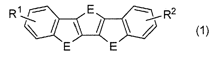
- substituted benzochalcogenoacene compound (1) represented by the formula (1) (hereinafter called “substituted benzochalcogenoacene compound (1) as the case may be") of the present invention will be explained in detail.
- Each of R 1 and R 2 independently represents a hydrogen atom, an optionally substituted C 4-30 alkyl group, an optionally substituted C 4-30 alkoxy group, an optionally substituted C 6-30 aryl group, an optionally substituted C 7-30 aralkyl group, an optionally substituted C 4-30 heteroaryl group, an optionally substituted C 5-30 heteroaralkyl group, or an optionally fluorinated C 3-30 trialkylsilyl group.
- at least one of R 1 and R 2 is not a hydrogen atom.
- the "C 4-30 alkyl group" in the "optionally substituted C 4-30 alkyl group” in R 1 and R 2 is any one of a linear, branched or cyclic alkyl group.
- the specific examples of the C 4-30 alkyl group include n-butyl, s-butyl, t-butyl, n-pentyl, neopentyl, n-hexyl, 2-ethylhexyl, n-heptyl, n-octyl, 2-hexyloctyl, n-nonyl, n-decyl, 2-hexyldecyl, n-undecyl, n-dodecyl, n-tridecyl, n-tetradecyl, n-pentadecyl, n-hexadecyl, n-heptadecyl, n-octadecy
- Examples of the substituent on the C 4-30 alkyl group include a halogen atom and a C 1-30 alkoxy group.
- Examples of the halogen atom include a fluorine atom, a chlorine atom and a bromine atom.
- Examples of the C 1-30 alkoxy group include methoxy, ethoxy, n-propoxy, n-butoxy, n-pentyloxy, n-hexyloxy, n-heptyloxy, n-octyloxy, n-nonyloxy, n-decyloxy, n-undecyloxy, n-dodecyloxy, n-tridecyloxy, n-tetradecyloxy, n-pentadecyloxy, n-hexadecyloxy, n-heptadecyloxy, n-octadecyloxy, n-nonadecy
- a fluorine atom is preferable as a substituent on the C 4-30 alkyl group.
- Examples of the fluorine atom-substituted C 4-30 alkyl group include perfluorohexyl, perfluorooctyl, perfluorodecyl, perfluorododecyl and perfluorotridecyl.
- Examples of the "C 4-30 alkoxy group" in the "optionally substituted C 4-30 alkoxy group” in R 1 and R 2 include n-butoxy, n-pentyloxy, n-hexyloxy, n-heptyloxy, n-octyloxy, n-nonyloxy, n-decyloxy, n-undecyloxy, n-dodecyloxy, n-tridecyloxy, n-tetradecyloxy, n-pentadecyloxy, n-hexadecyloxy, n-heptadecyloxy, n-octadecyloxy, n-nonadecyloxy, n-icosyloxy, n-henicosyloxy, n-docosyloxy, n-tricosyloxy, n-tetracosyloxy, n-pentacosyloxy, n
- C 4-20 alkoxy groups such as n-butoxy, n-pentyloxy, n-hexyloxy, n-heptyloxy, n-octyloxy, n-nonyloxy, n-decyloxy, n-undecyloxy, n-dodecyloxy, n-tridecyloxy, n-tetradecyloxy, n-pentadecyloxy, n-hexadecyloxy, n-heptadecyloxy, n-octadecyloxy, n-nonadecyloxy and n-icosyloxy are exemplified.
- substituent in the "optionally substituted C 4-30 alkoxy group” examples include halogen atoms such as a fluorine atom, a chlorine atom and a bromine atom, a C 1-30 alkoxy group, a C 6-30 aryl group, a C 7-30 aralkyl group, a C 4-30 heteroaryl group and a C 5-30 heteroaralkyl group.
- a hydrogen atom in the substituent may be substituted by a fluorine atom.
- the aryl group include phenyl, 1-naphthyl and 2-naphthyl.
- aralkyl group examples include the groups represented by the following formulae: wherein n1 represents an integer from 1 to 24, and each of n2 and n3 represents an integer from 1 to 20, respectively.
- the heteroaryl group means an aryl group in which at least one carbon atom among carbon atoms in the aromatic ring is replaced by a heteroatom such as a nitrogen atom, an oxygen atom, a sulfur atom or a selenium atom.
- heteroaryl group examples include thienyl, furyl, thiazolyl, thieno[3,2-b]thienyl, furoro[3,2-b]furyl, thieno[3,2-b]furyl, benzo[b]thienyl and benzo[b]furyl.
- heteroaryl group thienyl, thiazolyl, thieno[3,2-b]thienyl, benzo[b]thienyl and benzo[b]furyl are preferable.
- the heteroaralkyl group means a group in which at least one carbon atom in the aromatic ring in the aralkyl group is substituted by a heteroatom such as a nitrogen atom, an oxygen atom, a sulfur atom and a selenium atom.
- a heteroatom such as a nitrogen atom, an oxygen atom, a sulfur atom and a selenium atom.
- Examples of the heteroaralkyl group are represented by the following formulae: wherein n4 represents an integer from 1 to 26, n5 represents an integer from 1 to 24 and n6 represents an integer from 1 to 22. Further preferable examples are represented by the following formulae: wherein n4 represents an integer from 1 to 26, n5 represents an integer from 1 to 24 and n6 represents an integer from 1 to 22.
- a fluorine atom is preferable as a substituent in the C 4-30 alkoxy group.
- Examples of the substituted C 4-30 alkoxy group include perfluorohexyloxy, perfluorooctyloxy, perfluorodecyloxy, perfluorododecyloxy, perfluorotridecyloxy and methoxyethoxy.
- aryl group in the "optionally substituted C 6-30 aryl group” in R 1 and R 2 is, preferably, a monocyclic or bicyclic aryl group, and more preferably, phenyl, 1-naphtyl and 2-naphtyl.
- substituent in the "optionally substituted aryl group” examples include a halogen atom such as a fluorine atom, a chlorine atom and a bromine atom, a C 1-30 alkyl group, a C 1-30 alkoxy group, a C 6-30 aryl group, a C 7-30 aralkyl group, a C 4-30 heteroaryl group and a C 5-30 heteroaralkyl group.
- a hydrogen atom included in the substituent may be substituted by a fluorine atom.
- aryl group examples include phenyl, 1-naphtyl, 2-naphtyl, perfluorophenyl, 4-hexylphenyl and 4-hexyloxyphenyl.
- Examples of the C 1-30 alkyl group include methyl, ethyl, n-propyl, n-butyl, n-pentyl, n-hexyl, n-heptyl, n-octyl, n-nonyl, n-decyl, n-undecyl, n-dodecyl, n-tridecyl, n-tetradecyl, n-pentadecyl, n-hexadecyl, n-heptadecyl, n-octadecyl, n-nonadecyl, n-icosyl, n-henicosyl, n-docosyl, n-tricosyl, n-tetracosyl, n-pentacosyl, n-hexacosyl, n-heptacosyl, n-octacosyl,
- Examples of the substituent in the "optionally substituted C 7-30 aralkyl group" in R 1 and R 2 include a halogen atom such as a fluorine atom, a chlorine atom and a bromine atom, a C 1-30 alkyl group, a C 1-30 alkoxy group, a C 7-30 aralkyl group, a C 4-30 heteroaryl group and a C 5-30 heteroaralkyl group.
- the hydrogen atom in the substituent alkyl, alkoxy, aralkyl, heteroaryl or heteroaralkyl may be substituted by a fluorine atom.
- a fluorine atom is preferable.
- Examples of the "optionally substituted C 7-30 aralkyl group” include C 7-30 aralkyl groups represented by the following formulae: wherein n1 represents an integer from 1 to 24, and each of n2 and n3 represents an integer from 1 to 20, and substituted C 7-30 aralkyl groups represented by the following formulae: wherein each of n4 and n5 represents an integer from 1 to 24, and n6 represents an integer from 1 to 23.
- Examples of the "optionally substituted C 4-30 heteroaryl group" in R 1 and R 2 include thienyl, furyl, thiazolyl, thieno[3,2-b]thienyl, furolo[3,2-b]furyl, thieno[3,2-b]furyl, benzo[b]thienyl and benzo[b]furyl.
- the heteroaryl groups are exemplified by thienyl, thiazolyl, thieno[3,2-b]thienyl, benzo[b]thienyl and benzo[b]furyl, and more preferably exemplified by heteroaryl groups represented by the following formulae:
- substituent in the "optionally substituted heteroaryl group” examples include a halogen atom such as a fluorine atom, a chlorine atom or a bromine atom, a C 1-30 alkyl group, a C 1-30 alkoxy group, a C 6-30 aryl group, a C 7-30 aralkyl group, a C 4-30 heteroaryl group and a C 5-30 heteroaralkyl group.
- the hydrogen atom in the substituent may be substituted by a fluorine atom.
- heteroaryl groups are exemplified by 2-thienyl, 2-thieno[3,2-b]thienyl, 2-benzo[b]thienyl, 5-fuluoro-2-thienyl, 5-hexyl-2-thienyl and 4-hexyloxy-2-thienyl.
- substituent in the "optionally substituted C 5-30 heteroaralkyl group” examples include a halogen atom such as a fluorine atom, a chlorine atom and a bromine atom, a C 1-30 alkyl group, a C 1-30 alkoxy group, a C 7-30 aralkyl group, a C 4-30 heteroaryl group and a C 5-30 heteroaralkyl group.
- the hydrogen atom in the substituent may be substituted by a fluorine atom.
- a fluorine atom is preferable.
- Examples of the "optionally substituted C 5-30 heteroaralkyl group” include heteroaralkyl groups represented by the following formulae: wherein n4 represents an integer from 1 to 26, n5 represents an integer from 1 to 24 and n6 represents an integer from 1 to 22.
- the trialkylsilyl group in the "optionally fluorine atom-substituted C 3-30 trialkylsilyl group" in R 1 and R 2 is a silyl group in which the sum of the carbon atoms of alkyl groups connected to the silicon atom is 3 to 30.
- the maximum number of the carbon atoms in one alkyl group connected to the silicon atom is 28 and the alkyl group is an optionally fluorine atom-substituted C 1-30 alkyl group.
- the fluorine atom-substituted trialkylsilyl group means that a part or all of hydrogen atoms in the alkyl groups connected to the silicon atom are substituted by fluorine atoms.
- trialkylsilyl group examples include trimethylsilyl, triethylsilyl, tri(i-propyl)silyl, t-butyldimethylsilyl, dimethylhexylsilyl and dimethyldodecylsilyl.
- the bonding positions of R 1 and R 2 included in the substituted benzochalcogenoacene compound (1) of the present invention are preferably symmetrical.
- the symmetrical positions here can be illustrated using the following formula: wherein E, R 1 and R 2 have the same meanings as described above; that is, the symmetrical positions are explained as the cases in which R 1 is connected to a and R 2 is connected to a', R 1 is connected to b and R 2 is connected to b', R 1 is connected to c and R 2 is connected to c', and R 1 is connected to d and R 2 is connected to d'.
- Preferable case is exemplified by the case in which R 1 is connected to b and R 2 is connected to b', that is, a preferable compound is represented by the formula (2): wherein E, R 1 and R 2 have the same meanings as described above, or the case in which R 1 is connected to c and R 2 is connected to c', that is, a preferable compound is represented by the formula (3): wherein E, R 1 and R 2 have the same meanings as described above.
- Table 10-1 Compound No. E 1 E 2 E 3 R 1 R 2 166 S S S 167 S S S 168 S S S 169 S S S 170 S S S 171 S S S S 172 S S S 173 S S S 174 S S S 175 S S S S Dashed line indicates a chemical bond.
- Table 10-2 Compound No. E 1 E 2 E 3 R 1 R 2 176 S S S 177 S S S 178 S S S S 179 Se Se Se n-C 6 H 13 180 S S S 181 S S S 182 S Se S 183 S Se S 184 S Se S Dashed line indicates a chemical bond.
- substituted benzochalcogenoacene compounds (1) a compound is preferable in which three of E's in the benzochalcogenoacene compound (1) are all sulfur atoms.
- substituted benzochalcogenoacene compounds (1) having the following numbers in the above tables are preferably exemplified:
- the substituted benzochalcogenoacene compound (1) of the present invention is excellent in the solubility in the organic solvent, therefore, its handling is easy and its purification is easily carried out.
- a thin film can be also formed by dissolving the substituted benzochalcogenoacene compound (1) in the organic solvent, applying the solution and drying it.
- the thin film can be easily formed by the applying and film-forming process to be described hereinafter, since the substituted benzochalcogenoacene compound (1) is excellent in the solubility.
- the substituted benzochalcogenoacene compound (1) can provide a thin film showing high carrier mobility.
- a process for producing the substituted benzochalcogenoacene compound (1) is described below.
- a diacetylene compound which is represented, for example, by the formula (5-1) (hereinafter optionally described as a "compound (5-1)”): (wherein R 1 and R 2 represent the same meanings as described above, and X represents a halogen atom, preferably, a bromine atom), and subsequently, after dimetallation by a halogen-metal exchange reaction using an organometallic base (hereinafter, called a "present 1st reaction"), a dichalcogen-ene compound (optionally described as a "compound (4-1)") represented by the formula (4-1): (wherein E, R 1 and R 2 represent the same meanings as described above) is obtained by working of sulfur or selenium (hereinafter, optionally described as a "present 2nd reaction”).
- a mixture of the obtained compound (4-1) and a platinum compound such as biscyclooctadienyl platinum (Pt(COD) 2 ) or a copper compound such as a copper powder is heated in the absence of a solvent (hereinafter, optionally described as a "3rd-1 reaction"), or a mixture of the obtained compound (4-1), a nickel compound such as biscyclooctadienyl nickel (Ni(COD) 2 ) and a phosphine compound is heated and stirred in the presence of a solvent (optionally described as a "3rd-2 reaction").
- organometallic bases used in the present 1st reaction are exemplified by organolithium compounds such as methyllithium (MeLi), n-butyllithium (n-BuLi), sec-butyllithium (sec-BuLi) and tert-butyllithium (t-BuLi) and an organomagnesium compound such as an alkylgrignard compound.
- organolithium compound is preferable as the organometallic base.
- butyllithium (BuLi) can be used, and more preferably, t-butyl lithium (t-BuLi) can be used.
- the amount of the organometallic base to be used based on 1 mole of the compound (5-1) is, for example, in the range of 4 to 20 moles (in the range of 2 to 10 equivalents to 1 equivalent of a halogen atom), preferably in the range of 6 to 14 moles (in the range of 3 to 7 equivalents to 1 equivalent of a halogen atom), more preferably, in the range of 7 to 10 moles (in the range of 3.5 to 5 equivalents to 1 equivalent of the halogen atom).
- the amount of the organometallic base used is 4 moles or more, the unreacted amount of the compound (5-1) is reduced and the yield of the obtained compound (4-1) tends to increase.
- the amount used is 20 moles or less, a progress of a side reaction is suppressed and a purification of the compound (4-1) tends to become easy.
- the present 1st reaction and the succeeding 2nd reaction are preferable to be carried out in the presence of a solvent.
- the solvent used is selected from those which do not remarkably prevent the present 1st and 2nd reactions.
- aliphatic hydrocarbon solvents such as pentane, hexane and heptane, aromatic solvents such as benzene, toluene and xylene, ether solvents such as diethyl ether and tetrahydrofuran (THF) and the mixtures of 2 or more selected among them are used.
- a preferable solvent is the ether solvent.
- the present 1st reaction is carried out at temperatures of, for example, -20°C or lower, preferably, -40°C or lower, more preferably, -60°C or lower.
- the reaction time of the present 1st reaction can be controlled by the kind of organometallic bases or the solvents or by the reaction temperature, and the reaction time is in the range around from 10 minutes to 5 hours.
- the present second reaction is carried out.
- a sulfur (or selenium) may be used as purchased or may be added as a solution or a suspension dissolved or suspended in the solvent used in the present 1st reaction.
- the reaction temperature may be kept at a similar temperature to the present 1st reaction or may be heated in the temperature range which does not exceed the boiling point of the solvent used. Preferably, heating is carried out to reach the temperature range of 0 to 40°C, and subsequently, the temperature is kept in the same range.
- the reaction time is, for example, from 30 minutes to 72 hours.
- a crystalline, powder or colloidal sulfur (or selenium) can be used as the sulfur or selenium to be used in the present 2nd reaction.
- the amount of the sulfur or selenium used may be, for example, in the range of 4 to 20 moles, preferably, in the range of 6 to 14 moles, more preferably, in the range of 7 to 10 moles based on 1 mole of the compound (1-5). It is preferable to use the sulfur (or selenium) in the amount of 4 moles or more, since the yield of the compound (4-1) tends to increase in the molar range.
- the sulfur (or selenium) in the amount of 20 moles or less, since, in the molar range, a progress of a side reaction can be inhibited and a purification of the compound (4-1) tends to become easy.
- a solvent in the reaction mixture is optionally evaporated.
- an alkaline water solution such as a sodium hydroxide water solution or a potassium hydroxide water solution is added, and the obtained compound (4-1) is extracted.
- the solvent used in the present 1st and 2nd reactions is water, the solvent can be used directly as an extraction solvent.
- a halogenated hydrocarbon solvent such as dichloromethane or chloroform as the extraction solvent.
- the water phase is separated, then, to the water phase, a water solution of a hexacyanoferrate (III) salt such as potassium ferrycyanide is added, and subsequently, the compound (4-1) is extracted from the water phase by using an organic solvent such as said extraction solvent.
- a hexacyanoferrate (III) salt such as potassium ferrycyanide
- a copper compound or a platinum compound can be used in an amount of, for example, 0.5 to 20 moles, preferably 1 to 10 moles, more preferably 2 to 7 moles based on 1 mole of the compound (4-1).
- An example of the copper compound is a copper powder and an example of the platinum compound is biscyclooctadienyl platinum (Pt(COD) 2 ).
- a reaction temperature of the present 3rd-1 reaction is, for example, from 150 to 400°C, preferably, from 200 to 370°C.
- a reaction temperature of the present 3rd-1 reaction is within 1 hour, preferably, within 30 minutes.
- the reaction temperature is lowered to room temperature, and insoluble impurities are filtered off by using an organic solvent such as chloroform or dichloromethane which can dissolve the substituted benzochalcogenoacene compound (1).
- the filtrate is concentrated and optionally followed by application of column chromatography, recrystallization, etc. to result in the production of the substituted benzochalcogenoacene compound (1).
- a zero valent nickel compound such as biscyclooctadienyl nickel (Ni(COD) 2 ) is preferable as a nickel compound used in the present 3rd-1 reaction.
- the zero valent nickel compound may be formed in-situ by reduction of a two valent nickel compound such as bisacetylacetonato nickel (Ni(acac) 2 ) with a reducing agent such as diisobutylaluminum hydride.
- the amount of the nickel compound used is, for example, in a range of 0.5-5 moles, and preferably in a range of 0.7-3 moles based on 1 mole of the compound (4-1).
- Examples of a phosphine compound include triphenylphosphine, tricyclohexylphosphine, tri(o-tolyl)phosphine, trimethylphosphine, tri-t-butylphosphine, 1,2-(diphenylphosphino)ethane, 1,3-(diphenylphosphino)propane, 1,4-(diphenylphosphino)butane and 1,1-bis(diphenylphosphino)ferrocene.
- triphenylphosphine is preferable.
- the amount of the phosphine compound used is, for example, in a range of 0.5-20 moles of the phosphine compound, preferably, in a range of 0.7-10 moles based on 1 mole of the nickel compound.
- Examples of a solvent used in the present 3rd-2 reaction include an aliphatic hydrocarbon solvent such as pentane, hexane and heptane, an aromatic hydrocarbon solvent such as benzene, toluene and xylene, and a halogenated hydrocarbon solvent such as dichloromethane and chloroform. These solvents can be use alone or in a mixture of 2 or more of them.
- the aromatic hydrocarbon solvent is preferable, and toluene is more preferable as the solvent.
- the reaction temperature of the present 3rd-2 reaction is, for example, in a range from 10°C to a boiling point or lower of the solvent.
- the reaction time of the present 3rd-2 reaction is preferably within 72 hours depending on the reaction temperature.
- Table 47-1 Compound No. X 1 X 2 R 1 R 2 1306 Br Br 1307 Br Br 1308 Br Br 1309 Br Br 1310 Br Br 1311 Br Br 1312 Br Br 1313 Br Br 1314 Br Br 1315 Br Br Dashed line indicates a chemical bond.
- Table 47-2 Compound No. X 1 X 2 R 1 R 2 1316 Br Br 1317 Br Br 1318 Br Br 1319 Br Br Br n-C 6 H 13 1320 Br Br 1321 Br Br 1322 Br 1323 Br Br 1324 Br Dashed line indicates a chemical bond.
- Table 48-1 Compound No. X 1 X 2 R 1 R 2 1325 Br Br 1326 Br Br 1327 Br Br 1328 Br Br 1329 Br Br 1330 Br Br 1331 Br Br 1332 Br Br 1333 Br Br 1334 Br Br Dashed line indicates a chemical bond.
- Table 48-2 Compound No. X 1 X 2 R 1 R 2 1335 Br Br 1336 Br Br 1337 Br Br 1338 Br Br 1339 Br Br 1340 Br Br 1341 Br 1342 Br 1343 Br Br Dashed line indicates a chemical bond.
- Table 54-1 Compound No. X 1 X 2 R 1 R 2 1446 Br Br 1447 Br Br 1448 Br Br 1449 Br Br 1450 Br Br 1452 Br Br 1453 Br Br Dashed line indicates a chemical bond.
- Table 54-2 Compound No. X 1 X 2 R 1 R 2 1455 Br Br 1456 Br Br 1457 Br Br 1458 Br Br 1459 Br Br 1460 Br Br Dashed line indicates a chemical bond.
- Table 58-1 Compound No. X 1 X 2 R 1 R 2 1505 Br Br 1506 Br Br 1507 Br Br 1508 Br Br 1509 Br Br 1510 Br Br 1511 Br Br 1512 Br Br 1513 Br Br Dashed line indicates a chemical bond.
- Table 58-2 Compound No. X 1 X 2 R 1 R 2 1514 Br Br 1515 Br Br 1516 Br Br 1517 Br Br 1518 Br Br 1519 Br Br 1520 Br Br 1521 Br Dashed line indicates a chemical bond.
- Table 59-1 Compound No. X 1 X 2 R 1 R 2 1522 Br Br 1523 Br Br 1524 Br Br 1525 Br Br 1526 Br Br 1527 Br Br 1528 Br Br 1529 Br Br 1530 Br Br Dashed line indicates a chemical bond.
- Table 59-2 Compound No.
- Table 84-1 Compound No. E 1 E 2 E 3 R 1 R 2 736 S S S 737 S S S 738 S S S 739 S S S 740 S S S 741 S S S 742 S S S 743 S S S 744 S S S 745 S S S Dashed line indicates a chemical bond.
- Table 84-2 Compound No. E 1 E 2 E 3 R 1 R 2 746 S S S 747 S S S 748 S S S 749 Se Se Se n-C 6 H 13 750 S S S 751 S S S 752 S Se S 753 S Se S 754 Se S Se Dashed line indicates a chemical bond.
- Table 85-1 Compound No. E 1 E 2 E 3 R 1 R 2 755 S S S 756 S S S 757 S S S 758 S S S 759 S S S 760 S S S S 761 S S S 762 S S S 763 S S S 764 S S S Dashed line indicates a chemical bond.
- Table 85-2 Compound No. E 1 E 2 E 3 R 1 R 2 765 S S S 766 S S S 767 S S S 768 S S S 769 S S S S 770 S S S 771 S S S 772 S S S 773 S S S Dashed line indicates a chemical bond.
- the compound (5-1) used for the present 1st reaction is described for the case that R 1 and R 2 are the same kinds (hereinafter, optionally described as R) as follows. That is, the compound (5-1) can be produced by the so-called Glaser Reaction, the Eglinton Coupling or the Hay Coupling (preferably, the Hay Coupling utilizing a copper compound such as copper iodide) by using, for example, a compound represented by the formula (6-1): (wherein R represents the same meaning as R 1 and R 2 , and X represents a halogen atom, preferably, a bromine atom).
- the Hay Coupling can be carried out, for example, in the presence of N,N,N',N'-tetramethyethylnediamine (TMEDA) and a copper compound such as copper iodide according to the reaction formula below.
- TEDA N,N,N',N'-tetramethyethylnediamine
- a copper compound such as copper iodide according to the reaction formula below.
- the compound of the formula (6-1) can be produced, for example, by the process comprising steps of:
- Table 112 Compound No. X 1 R 1 1711 Br n-C 4 H 9 1712 Br s-C 4 H 9 1713 Br n-C 5 H 11 1714 Br 1715 Br n-C 6 H 13 1716 Br 1717 Br 1718 Br n-C 7 H 15 1719 Br n-C 8 H 17 1720 Br n-C 9 H 19 1721 Br n-C 10 H 21 1722 Br 1723 Br n-C 11 H 23 1724 Br n-C 12 H 25 1725 Br n-C 13 H 27 Dashed line indicates a chemical bond.
- Table 121-1 Compound No. X 1 R 1 1876 Br 1877 Br 1878 Br 1879 Br 1880 Br 1881 Br 1882 Br 1883 Br 1884 Br Dashed line indicates a chemical bond.
- Table 121-2 Compound No. X 1 R 1 1885 Br 1886 Br 1887 Br 1888 Br 1889 Br 1890 Br 1891 Br 1892 Br 1893 Br 1894 Br Dashed line indicates a chemical bond.
- Table 122-1 Compound No. X 1 R 1 1895 Br 1896 Br 1897 Br 1898 Br 1899 Br 1900 Br 1901 Br 1902 Br 1903 Br 1904 Br Dashed line indicates a chemical bond.
- Table 122-2 Compound No. X 1 R 1 1905 Br 1906 Br 1907 Br 1908 Br 1909 Br 1910 Br 1911 Br 1912 Br 1913 Br Dashed line indicates a chemical bond.
- Table 128-1 Compound No. X 1 R 1 2016 Br 2017 Br 2018 Br 2019 Br 2020 Br 2022 Br 2023 Br Dashed line indicates a chemical bond.
- Table 128-2 Compound No. X 1 R 1 2025 Br 2026 Br 2027 Br 2028 Br 2029 Br 2030 Br Dashed line indicates a chemical bond.
- Table 132-1 Compound No. X 1 R 1 2075 Br 2076 Br 2077 Br 2078 Br 2079 Br 2080 Br 2081 Br 2082 Br 2083 Br Dashed line indicates a chemical bond.
- Table 132-2 Compound No. X 1 R 1 2084 Br 2085 Br 2086 Br 2087 Br 2088 Br 2089 Br 2090 Br 2091 Br Dashed line indicates a chemical bond.
- Table 133-1 Compound No. X 1 R 1 2092 Br 2093 Br 2094 Br 2095 Br 2096 Br 2097 Br 2098 Br 2099 Br 2100 Br Dashed line indicates a chemical bond.
- Table 133-2 Compound No. X 1 R 1 2101 Br 2102 Br 2103 Br 2104 Br -Si(CH 3 ) 3 2105 Br -Si(C 2 H 5 ) 3 2106 Br -Si(i-C 3 H 7 ) 3 2107 Br -Si(CH 3 ) 2 (t-C 4 H 9 ) 2108 Br -Si(CH 3 ) 2 (n-C 6 H 13 ) 2109 Br -Si(CH 3 ) 2 (n-C 12 H 25 ) Dashed line indicates a chemical bond.
- a process for producing the substituted benzochalcogenoacene compound (1) in the case that R 1 and R 2 are the same or different kinds, is exemplified by a process according to the description of the non-patent literature 1 ( Advanced Materials, 19, 3008-3011 (2007 )). That is, the process comprises the sequential steps of:
- a thin film of the present invention comprises the substituted benzochalcogenoacene compound (1).
- the thin film shows high carrier mobility. Therefore, the thin film is suitable for a material for an organic semiconductor device having the thin film as an active organic semiconductor layer.
- the organic semiconductor device of the present invention comprises the thin film of the present invention.
- Examples of the organic semiconductor device of the present invention include an organic transistor, an electroluminescence device and a solar cell.
- the organic transistor of the present invention can be used, for example, in an electronic paper, a flexible display, an IC tag and a sensor.
- the formation process of the thin film of the present invention is exemplified by the applying and film-forming process.
- the applying and film-forming process means the film-forming process which comprises the steps of dissolving the substituted benzochalcogenoacene compound (1) in a solvent and applying the obtained solution composition on a substrate or an insulating layer.
- the coating process include a casting process, a dip coat process, a die coater process, a roll coater process, a bar coater process, an ink jet process, a screen printing process, an offset printing process and a microcontact printing process. These processes can be used alone or in combination of two or more of these processes.
- a relevant solvent which is used for the preparation of the above solution composition can be selected properly depending on the kind of the substituted benzochalcogenoacene compound to be applied.
- the solvent include an aromatic hydrocarbon solvent such as benzene, toluene, xylene, chlorobenzene and o-dichlorobenzene, a halogenated hydrocarbon solvent such as dichloromethane, chloroform, 1,2-dichloroethane, 1,1',2,2'-tetrachloroethane, tetrachlorocarbon, an ether solvent such as tetrahydrofuran and dioxane, and an aliphatic hydrocarbon solvent such as pentane, hexane, heptane, octane and cyclohexane.
- the concentration of the substituted benzochalcogenoacene compound (1) in the solution composition is 0.01-50 wt%, preferably, 0.01-10 wt%, more preferably, 0.1-5 wt%. Additionally, within the range where carrier mobility is not damaged remarkably, additives such as an antioxidant or a stabilizer can be contained in the solution composition.
- the solution composition can be obtained by dissolving the substituted benzochalcogenoacene compound (1) in the solvent at temperatures of, for example, 10-200°C, preferably, 20-150°C.
- a thin film can be formed on the substrate or the insulating layer by eliminating the solvent contained in the coated film.
- a naturally drying treatment, a heating treatment, a reduced pressure treatment, a draught drying treatment and a combination thereof can be adopted.
- the naturally drying treatment or the heating treatment are preferable from the point of easy operation.
- the operation condition for the treatment is described as still-standing under the atmosphere or heating of the substrate on a hot plate (for example, at 40-250°C, preferably, 50-250°C).
- the thin film of the present invention can be formed by the applying and film-forming process by using also a dispersion of the substituted benzochalcogenoacene compound (1) in the solvent, and in this case, the process can be easily carried out by reading the solution composition as the dispersion composition.
- the thin film of the present invention can be formed by a simple method such as the applying and film-forming process as described above.
- Another different example of the thin film forming process of the present invention is a thin film forming process under vacuum such as a vacuum deposition process, a sputtering process, a CVD process and a molecular beam epitaxial process.
- the substituted benzochalcogenoacene compound is heated in a crucible or a metal boat under vacuum, and the evaporated organic semiconductor material is deposited on the substrate or the insulating material.
- a degree of vacuum when deposition occurs is, generally, 1x10 -1 Pa or lower, preferably, 1x10 -3 Pa or lower.
- a substrate temperature when deposition occurs is, generally, 0°C -300°C, preferably, 20°C -200°C.
- a deposition speed is, for example, 0.001nm/sec - 10nm/sec, preferably, 0.01nm/sec - 1nm/sec.
- a thickness of the thin film comprising the substituted benzochalcogenoacene compound (1) obtained by the above applying and film-forming process or the above vacuum process is controllable, for example, depending on a device structure of the organic transistor, and the film thickness is preferably 1nm-10 ⁇ m, more preferably, 5nm-1 ⁇ m.
- An example of the organic transistor of the present invention is the organic field effect transistor (OFET).
- the structure of the organic field effect transistor is, for example, generally provided with a source electrode and a drain electrode close to the organic semiconductor active layer consisting of the thin film of the present invention, and further provided with a gate electrode across an insulator layer (a dielectric layer) close to the organic semiconductor active layer.
- Examples of the device structure include the followings:
- materials constituting the source electrode, the drain electrode and the gate electrode are not limited specifically as far as the materials are electrically conducting materials such as platinum, gold, silver, nickel, chromium, copper, iron, tin, lead antimony, tantalum, indium, palladium, tellurium, rhenium, iridium, aluminum, ruthenium, germanium, molybdenum, molybdenum oxide, tungsten, antimony tin oxide, indium tin oxide (ITO), zinc doped with fluorine, zinc, carbon, graphite, a glassy carbon, a silver paste and carbon paste, lithium, beryllium, sodium, magnesium, potassium, calcium, scandium, titanium, manganese, zirconium, gallium, niobium, sodium, a sodium-potassium alloy, magnesium, lithium, aluminum, a magnesium/ copper mixture, a magnesium/silver mixture, a magnesium/
- electrically conducting materials such as platinum, gold, silver, nickel, chromium, copper, iron,
- conductive polymers whose conductivity is improved by doping, etc. are also suitably used.
- conductive polymers include a conductive polyaniline, a conductive polypyrrole, a conductive polythiophene and a complex between polyethylenedioxythiophene and polystyrene sulfonic acid.
- the conductive materials which have a low electric resistance at the contact face with the semiconductor layer are preferable. These conductive materials may be used alone or in a mixture of two or more kinds.
- a film thickness of the electrode varies depending on the material, and the thickness is, preferably, 0.1nm-10 ⁇ m, further preferably, 0.5nm-5 ⁇ m, and more preferably, 1nm-3 ⁇ m.
- the film thickness may be larger than the above values.
- the source electrode and the drain electrode used in the organic transistor of the present invention may undergo a surface treatment.
- the surface treatment of the electrode surface contacting with the thin film (the organic semiconductor active layer) of the present invention is preferable, since the surface treatment tends to improve the transistor performances of the organic transistor comprising the thin film.
- An example of the surface treatment is a modification process of the electrode surfaces mentioned above by dipping the electrodes in an alcohol solution of, for example, a saturated hydrocarbon compound having a thiol group such as 1-octylthiol, 1-perfluorooctylthiol, 1-octadecylthiol and 1-perfluorooctadecylthiol, an aromatic compound having a thiol group such as benzenethiol and perfluorobenzenethiol, and a heteroaromatic compound having a thiol group such as thienylthiol and perfluoro-thienylthiol.
- a saturated hydrocarbon compound having a thiol group such as 1-octylthiol, 1-perfluorooctylthiol, 1-octadecylthiol and 1-perfluorooctadecylthiol, an aromatic compound having a thi
- the electrode can be manufactured by various methods using above raw materials. Specifically, a vacuum deposition method, a sputtering method, a coating method, a thermal transfer method, a printing method and a sol-gel method are exemplified. At or after the film-forming, it is preferable to carry out patterning, optionally.
- the patterning can be carried out by using various methods. Specifically, a photolithography method which combines a patterning and an etching of the photoresist is exemplified. In addition, soft-lithography methods such as an inkjet printing, a screen printing, an offset printing and an anastatic printing are exemplified. These methods can be used for the patterning, alone or in combination of two or more of them.
- Inorganic oxides, inorganic nitrides and organic compounds can be exemplified as materials for the insulating films.
- examples of inorganic oxides include silicon oxide, aluminum oxide, tantalum oxide, titanium oxide, tin oxide, vanadium oxide, strontium barium titanate, barium titanate zirconate, lead titanate zirconate, lanthanum lead titanate, strontium titanate, barium titanate, magnesium barium fluoride, bismuth titanate, bismuth strontium titanate, bismuth strontium tantalite, bismuth niobate tantalite and yttrium trioxide.
- Silicon oxide, aluminum oxide, tantalum oxide and titanium oxide are preferable.
- the organic compounds include polyimide, polyamide, polyester, polyacrylate, a photo-curable resin obtained by photo-radical polymerization or photo-cationic polymerization, a copolymer comprising an acrylonitrile component, polyvinylphenol, polyvinylalcohol, a novolak resin and cyanoethylpullulan.
- Polyimide, polyvinylphenol and polyvinylalcohol are preferable.
- These materials for the insulating layer can be used alone or in combination of two or more of them.
- a thickness of the insulating layer varies depending on the material, and the thickness is, preferably, 0.1nm-100 ⁇ m, further preferably, 0.5nm-50 ⁇ m, and more preferably, 5nm-10 ⁇ m.
- the insulating layer can be formed by various methods. Specifically, a spin coating, a spray coating, a dip coating, a cast, a bar coating, a blade coating, a screen printing, an offset printing, an inkjet and dry process methods such as a vacuum deposition, a molecular beam epitaxial growth method, an ion cluster beam method, an ion plating method, a sputtering method, an atmospheric plasma method and a CVD method are exemplified. In addition, a sol-gel method and a method in which an oxide film is formed on a metal substrate such as an alumite on aluminum or a thermal oxide film of silicon are exemplified.
- the materials of the substrate include glass, paper, quartz, ceramic and a resin sheet.
- materials for the resin sheet include polyethylene terephthalate (PET), polyethylene naphthalate (PEN), polyether sulfone (PES), polyetherimide, polyether ether ketone, polyphenylene sulfide, polyarylate, polyimide, polycarbonate (PC), cellulose triacetate (TAC) and cellulose acetate propionate (CAP).
- PET polyethylene terephthalate
- PEN polyethylene naphthalate
- PES polyether sulfone
- polyetherimide polyether ether ketone
- polyphenylene sulfide polyarylate
- polyimide polycarbonate
- PC cellulose triacetate
- CAP cellulose acetate propionate
- the thickness of the substrate is, preferably, 1 ⁇ m-10mm, more preferably, 5 ⁇ m-5mm.
- a surface treatment may be carried out on the insulating layer and the substrate.
- the transistor performance of the organic transistor can be improved.
- the surface treatment is exemplified specifically by a hydrophorbic treatment by hexamethyldisilazane, octadecyltrichlorosilane, octyltrichlorosilane and phenetyltrichlorosilane, an acid treatment by hydrochloric acid, sulfuric acid and an aqueous hydrogen peroxide solution, an alkaline treatment by sodium hydroxide, potassium hydroxide, calcium hydroxide and an aqueous ammonia, an ozone treatment, a hydrogen fluoride treatment, a plasma treatment such as oxygen and argon, a film-forming treatment of Langmuir-Brodgett film, a thin-film forming treatment of other insulator and semiconductor films, a mechanical treatment, an electric treatment such as corona discharge and a rubbing treatment using fibers.
- a hydrophorbic treatment by hexamethyldisilazane
- octadecyltrichlorosilane
- Processes for the surface treatment are exemplified by a vacuum deposition process, a sputtering process, a coating process, a printing process and a sol-gel process.
- a protective film consisting of resins or inorganic compounds may be laminated on the organic semiconductor active layer.
- the formation of the protective film inhibits influences from the outer circumstances to result in stabilization of the transistor drive.
- the thin film of the present application exhibits a high carrier-mobility, since it comprises the substituted benzochalcogenoacene compound (1). Therefore, the thin film of the present application is useful as the organic semiconductor active layer in the organic transistor, and the organic transistor having the organic semiconductor active layer comprising the thin film of the present invention exhibits excellent transistor performances and is useful for the organic semiconductor device.
- the organic phase was extracted and dried with sodium sulfate, followed by condensation by the evaporator to give an oil product.
- the oil product was purified by a silica gel column to give 2-bromo-4-hexylaniline (35.63g, 139.1mmol, yield 48.8%).
- reaction mixture was refluxed for 20 minutes by heating, and then cooled to the room temperature. Subsequently, the reaction mixture was poured into an aqueous solution (water 450mL) of sodium sulfite (22.5g, 216.2mmol). Ethyl acetate was added to the reaction mixture, then, the organic phase was extracted, dried with magnesium sulfate and condensed by the evaporator to result in the formation of a brown oil (28.15 g) which contains 2-bromo-4-hexyl-1-iodobenzene as a main component (76.7mmol, yield 76.7%).
- the compound [1145] (10.6g, 20mmol) obtained in the Preparation example 4 was dissolved in THF 200mL, and to this solution, under nitrogen atmosphere at -78°C, a 1.59M pentane solution (62.9mL, 100.0mmol) of t-BuLi was added in drops. After stirring at -78°C for 1 hour, a sulfur powder (3.2g, 100.0mmol) was added by small pieces, and subsequently, the temperature was slowly raised to room temperature and stirring was continued for 2 hours. A 1M sodium hydroxide solution (300mL) and K 3 Fe (CN) 6 (32.9g, 100.0mmol) were added, and after stirring for 1 hour at room temperature, chloroform was added to extract the organic phase.
- Example 3 Formation of a thin film consisting of the compound [5] by vacuum deposition method and manufacture of an organic transistor having the thin film>
- Electrodes of chromium in 3nm and gold in 50nm deposited in this order were formed by the vapor deposition method using a metal mask on the substrate laminated with hexamethyldisilazane by spin coating over n-doped silicon wafer having a thermally oxidized SiO 2 film.
- Each of a channel width and a channel length of the electrode formed was 2000 ⁇ m and 20 ⁇ m, respectively.
- the compound [5] synthesized in Example 1 and purified by sublimation was put into a quartz crucible, and the crucible was heated to form a thin film consisting of the compound [5] by the vacuum deposition method.
- the degree of vacuum in the apparatus chamber used for the vacuum deposition method was 1 ⁇ 10 -4 pascal or lower, and the temperature of the substrate was in a range from room temperature (24°) to 80°C or lower.
- the thickness of the thin film was about 200nm.
- each of L and W represents a channel length and a channel width of the organic transistor, respectively
- Ci represents an electrostatic capacitance per unit area of an insulating layer for the gate electrode (hereinafter, optionally described as a gate insulating film)
- Vg represents a gate voltage
- Vt represents a threshold value voltage of the gate voltage.
- the saturated field-effect mobility ⁇ of the carrier in the organic transistor having the thin film consisting of the compound [5] and manufactured was calculated by using the formula (a), and the following results were obtained. That is, the saturated field-effect mobility of the carrier (carrier mobility) in the organic transistor having the thin film consisting of the compound [5] and manufactured at a substrate temperature of 60°C was 1.6cm 2 /Vs. In addition, the ratio of the drain currents Ids at the gate voltages of 0 V and - 50 V (hereinafter, optionally described as on/of ratio) at the drain voltage Vd of -50 V was 10 7 .
- the solution composition containing the compound [5] in 0.5 wt% concentration was prepared by dissolving the compound [5] manufactured in Example 1 in tetrahydrofuran. This solution composition was applied on the n-doped silicon wafer having a thermally oxidized SiO 2 film treated with hexamethyldisilazane using a spin coat method, and thus, the thin film consisting of the compound [5] was formed. In addition, the formed thin film was kept at 80°C for 30 minutes. The thickness of the thin film was about 30nm.
- Example 5 On the thin film obtained in Example 5, a molybdenum oxide layer and successively a gold layer were formed using a metal mask by the vacuum deposition method, and thus, a source electrode and a drain electrode were formed.
- each of a channel width and a channel length of the organic TFT obtained by forming the source electrode and the drain electrode was 2000 ⁇ m and 20 ⁇ m, respectively.
- the organic transistor having the thin film comprising the compound [5] as shown in Fig. 2 was manufactured.
- Example 6 The electric performances of the organic transistor manufactured in Example 6 were also measured similarly to Example 4. The results showed that each of the field-effect mobility of the carrier (carrier mobility) and the on/off ratio was 0.3cm 2 /Vs and 10 7 , respectively.
- Example 8 Manufacture of the organic transistor having a thin film consisting of the compound [14] >
- a source electrode and a drain electrode in the sequence of chromium and gold starting from the thermally oxidized SiO 2 film having a channel width of 2000 ⁇ m and a channel length of 20 ⁇ m were formed.
- the substrate was washed with acetone in ultrasonic bath for 10 minutes and irradiated by an ozone UV for 20 minutes. Then, the substrate surface was silanized by dipping the substrate in the toluene diluent solution of phenylethyltrichlorosilane for 2 minutes.
- the surface of the Au electrode formed on the substrate was modified by dipping the substrate in the isopropyl alcohol diluent solution of perfluorobenzene thiol for 2 minutes, and thus, the transistor substrate was manufactured. Then, the compound [14] synthesized in Example 2 was put into the crucible, the crucible was heated, and thus, by the vacuum deposition method, a thin film consisting of the compound [14] was formed on the transistor substrate. A vacuum degree in the apparatus chamber used for the vacuum deposition was 1 ⁇ 10 -4 pascal or less and the substrate temperature was 80°C. A thickness of the thin film was about 100nm.
- a thin film was formed by the vacuum deposition method according to the same procedure as Example 3 except using the compound C-1 represented by the above formula and disclosed in the patent document 1, then followed by manufacturing the organic transistor having the thin film.
- the electric performances of the obtained organic transistor were measured according to Example 4, and the results showed that the carrier mobility and the on/off ratio of the obtained organic transistor were 10 -5 cm 2 /Vs and 10 3 , respectively.
- Example 12 Preparation of the compound [14], formation of a thin film consisting of the compound [14] by the applying and film-forming process, and manufacture and measurement of a transistor having the thin film>
- the compound [14] (which means the compound No. 41 in Table 2) can be obtained according to similar procedures to Preparation examples 7 and 8 and Example 2 except that 4-pentyloxyaniline is used instead of 4-dodecylaniline.
- a transistor substrate is prepared according to a similar procedure to Example 8
- an organic transistor having the thin film is produced according to a similar procedure to Example 10.
- a high value of the carrier mobility can be obtained.
- the compound [155] (which means the compound No. 155 in Table 9) can be obtained according to similar procedures to Preparation examples 7 and 8 and Example 2 except that 4-(4-phenylbutul)aniline is used instead of 4-dodecylaniline.
- a transistor substrate is prepared according to a similar procedure to Example 8
- an organic transistor having the thin film is produced according to a similar procedure to Example 10.
- a high value of the carrier mobility can be obtained.
- the compound [222] (which means the compound No. 222 in Table 13) can be obtained according to similar procedures to Preparation examples 7 and 8 and Example 2 except that 3-octylaniline is used instead of 3-octylaniline in Preparation example 1.
- a transistor substrate is prepared according to a similar procedure to Example 8
- an organic transistor having the thin film is produced according to a similar procedure to Example 10.
- a high value of the carrier mobility can be obtained.
- the compound [7] (which means the compound No. 7 in Table 1) can be obtained according to similar procedures to Preparation examples 7 and 8 and Example 2 except that 4-(2-ethylhexyl)aniline is used instead of 4-dodecylaniline.
- the compound [12] (which means the compound No. 12 in Table 1) can be obtained according to similar procedures to Preparation examples 7 and 8 and Example 2 except that 4-(2-hexyldecyl)aniline is used instead of 4-dodecylaniline.
- the compound [15] (which means the compound No. 15 in Table 1) can be obtained according to similar procedures to Preparation examples 7 and 8 and Example 2 except that 4-tridecylaniline is used instead of 4-dodecylaniline.
- the compound [18] (which means the compound No. 18 in Table 2) can be obtained according to similar procedures to Preparation examples 7 and 8 and Example 2 except that 4-hexadecylaniline is used instead of 4-dodecylaniline.
- the compound [42] (which means the compound No. 42 in Table 2) can be obtained according to similar procedures to Preparation examples 7 and 8 and Example 2 except that 4-(2-hexyloctyl)aniline is used instead of 4-dodecylaniline.
- the compound [84] (which means the compound No. 84 in Table 4) can be obtained according to similar procedures to Preparation examples 7 and 8 and Example 2 except that 4-(4'-hexylphenyl)aniline is used instead of 4-dodecylaniline.
- the compound [97] (which means the compound No. 97 in Table 5) can be obtained according to similar procedures to Preparation examples 7 and 8 and Example 2 except that 4-(2-(5-hexyl)thienyl) aniline is used instead of 4-dodecylaniline.
- the compound [205] (which means the compound No. 205 in Table 12) can be obtained according to similar procedures to Preparation examples 7 and 8 and Example 2 except that 4-[(2-benzo[b]thieno)octyl]aniline is used instead of 4-dodecylaniline.
- the compound [208] (which means the compound No. 208 in Table 12) can be obtained according to the following formula in the document: Advanced Materials, 19, 3008-3011 (2007 ):.
- the present invention can provide the new substituted benzochalcogenoacene compound, the thin film comprising the compound and the organic semiconductor device comprising the thin film.
Landscapes
- Chemical & Material Sciences (AREA)
- Organic Chemistry (AREA)
- Engineering & Computer Science (AREA)
- Materials Engineering (AREA)
- Physics & Mathematics (AREA)
- Spectroscopy & Molecular Physics (AREA)
- Thin Film Transistor (AREA)
- Heterocyclic Carbon Compounds Containing A Hetero Ring Having Oxygen Or Sulfur (AREA)
- Electroluminescent Light Sources (AREA)
Abstract
Description
- The present invention relates to a substituted benzochalcogenoacene compound, a thin film comprising the compound and an organic semiconductor device comprising the thin film.
- In the non patent document 1, is described dibenzo[d,d']thieno[3,2-b; 4,5'-b']dithiophene, and in the patent document 1, is described a dibenzochalcogenoacene compound represented by the following formula:

- Patent Document 1:
W02005/087780 [Formula 11] - Non-patent Document 1: Adv. Mater., 2007, 19, 3008-3011
- In the circumstances mentioned above, a suitable new compound as an organic semiconductor material has been investigated.
- In order to solve these problems, we, the inventors of the present application have made intensive studies on the substituted benzochalcogenoacene compounds, and have attained the following inventions.
That is, the present invention provides: - <1> A substituted benzochalcogenoacene compound represented by the formula (1):

- <2> The compound according to <1> wherein all E's in the formula (1) are sulfur atoms;
- <3> The compound according to <1> or <2> wherein each of R1 and R2 in the formula (1) independently represents a hydrogen atom, an optionally fluorinated C4-30 alkyl group, an optionally fluorinated C4-30 alkoxy group, an optionally alkylated or alkoxylated C6-30 aryl group which is optionally fluorinated, an optionally fluorinated C7-30 aralkyl group, an optionally alkylated or alkoxylated C4-30 heteroaryl group which is optionally fluorinated, or an optionally fluorinated C5-30 heteroaralkyl group;
- <4> The compound according to any one of <1> to <3> wherein the compound represented by the formula (1) is a compound represented by the formula (2):

- <5> The compound according to <4> wherein, in the formula (2), each E independently represents a sulfur or selenium atom, and each of R1 and R2 independently represents a hydrogen atom, an optionally fluorinated C4-30 alkyl group, or an optionally alkylated or fluorinated C3-30 trialkylsilyl group;
- <6> The compound according to <5> wherein each of R1 and R2 in the formula (2) independently represents a C4-30 alkyl group or a C3-30 trialkylsilyl group;
- <7> The compound according to <5> wherein R1 and R2 in the formula (2) represent C4-30 alkyl groups;
- <8> The compound according to <5> wherein R1 and R2 in the formula (2) are the same and represent C4-20 alkyl groups;
- <9> The compound according to <5> wherein R1 and R2 in the formula (2) represent C6-12 alkyl groups;
- <10> The compound according to <4> wherein each of R1 and R2 in the formula (2) independently represents a hydrogen atom, an optionally fluorinated C4-30 alkyl group, an optionally fluorinated C4-30 alkoxy group, an optionally alkylated C6-30 aryl group which is optionally fluorinated, or an optionally fluorinated C7-30 aralkyl group;
- <11> The compound according to <4> wherein R1 and R2 in the formula (2) are the same and represent C4-20 alkoxy groups;
- <12> The compound according to <4> wherein R1 and R2 in the formula (2) are the same and represent C6-10 aryl groups having C1-20 alkyl groups;
- < 13> The compound according to <4> wherein R1 and R2 in the formula (2) are the same and represent C7-20 aralkyl groups;
- < 14> The compound according to <5> wherein each of R1 and R2 in the formula (2) independently represents a C3-30 trialkylsilyl group;
- < 15> The compound according to <5> wherein each of R1 and R2 in the formula (2) independently represents a C3-14 trialkylsilyl group;
- <16> The compound according to <4> or <5> wherein R1 and R2 in the formula (2) are the same and represent hexyl or dodecyl;
- < 17> The compound according to any one of <4> to < 16> wherein all E's in the formula (2) represent sulfur atoms;
- < 18> The compound according to <4> wherein all E's in the formula (2) represent sulfur atoms, and R1 and R2 in the formula (2) are the same and represent hexyl;
- < 19> The compound according to <4> wherein all E's in the formula (2) represent sulfur atoms, and R1 and R2 in the formula (2) are the same and represent dodecyl;
- <20> The compound according to <4> wherein all E's in the formula (2) represent sulfur atoms, and each of R1 and R2 in the formula (2) independently represents a C6-12 alkyl group.
- <21> A compound represented by the formula [5], [7], [12], [15], [18] or [42] below:


- <22> The compound according to any one of <1> to <3> wherein the compound represented by the formula (1) is a compound represented by the formula (3):

- <23> The compound according to <22> wherein R1 and R2 in the formula (3) are the same and represent C4-20 alkyl groups;
- <24> A thin film comprising the compound according to any one of <1> to <23>;
- <25> A thin film consisting of the compound according to any one of <1> to <23>:
- <26> An organic semiconductor device comprising the thin film according to <24> or <25>;
- <27> An organic transistor comprising the thin film according to <24> or <25>.
- The present invention can provide novel substituted benzochalcogenoacene compounds.
-
-
Figure 1 is a cross-section diagram illustrating one embodiment of the organic transistor in the present invention. -
Figure 2 is a cross-section diagram illustrating one embodiment of the organic transistor in the present invention. - First of all, the substituted benzochalcogenoacene compound represented by the formula (1) (hereinafter called "substituted benzochalcogenoacene compound (1) as the case may be") of the present invention will be explained in detail.
Each E in the formulae (1), (2) and (3) independently represents a sulfur or selenium atom. Each of R1 and R2 independently represents a hydrogen atom, an optionally substituted C4-30 alkyl group, an optionally substituted C4-30 alkoxy group, an optionally substituted C6-30 aryl group, an optionally substituted C7-30 aralkyl group, an optionally substituted C4-30 heteroaryl group, an optionally substituted C5-30 heteroaralkyl group, or an optionally fluorinated C3-30 trialkylsilyl group. However, at least one of R1 and R2 is not a hydrogen atom. - The "C4-30 alkyl group" in the "optionally substituted C4-30 alkyl group" in R1 and R2 is any one of a linear, branched or cyclic alkyl group. The specific examples of the C4-30 alkyl group include n-butyl, s-butyl, t-butyl, n-pentyl, neopentyl, n-hexyl, 2-ethylhexyl, n-heptyl, n-octyl, 2-hexyloctyl, n-nonyl, n-decyl, 2-hexyldecyl, n-undecyl, n-dodecyl, n-tridecyl, n-tetradecyl, n-pentadecyl, n-hexadecyl, n-heptadecyl, n-octadecyl, n-nonadecyl, n-icosyl, n-henicosyl, n-docosyl, n-tricosyl, n-tetracosyl, n-pentacosyl, n-hexacosyl, n-pehptacosyl, n-octacosyl, n-nonacosyl, n-triacontyl, cyclopentyl, cyclohexyl and cycloheptyl, and preferably, n-butyl, s-butyl, t-butyl, n-pentyl, neopentyl, n-hexyl, 2-ethylhexyl, n-heptyl, n-octyl, n-nonyl, n-decyl, 2-hexyldecyl, n-undecyl, n-dodecyl, n-tridecyl, n-tetradecyl, n-pentadecyl, n-hexadecyl, n-heptadecyl, n-octadecyl, n-nonadecyl, n-icosyl, and more preferably, a C4-16 alkyl group such as n-butyl, n-pentyl, n-hexyl, cyclohexyl, 2-ethylhexyl, n-heptyl, n-octyl, n-nonyl, n-decyl, n-undecyl, n-dodecyl, n-tridecyl, 2-hexyloctyl, n-tetradecyl, n-pentadecyl, n-hexadecyl, cyclohexyl and cycloheptyl.
- Examples of the substituent on the C4-30 alkyl group include a halogen atom and a C1-30 alkoxy group.
Examples of the halogen atom include a fluorine atom, a chlorine atom and a bromine atom.
Examples of the C1-30 alkoxy group include methoxy, ethoxy, n-propoxy, n-butoxy, n-pentyloxy, n-hexyloxy, n-heptyloxy, n-octyloxy, n-nonyloxy, n-decyloxy, n-undecyloxy, n-dodecyloxy, n-tridecyloxy, n-tetradecyloxy, n-pentadecyloxy, n-hexadecyloxy, n-heptadecyloxy, n-octadecyloxy, n-nonadecyloxy, n-icosyloxy, n-henicosyloxy, n-docosyloxy, n-tricosyloxy, n-tetracosyloxy, n-pentacosyloxy, n-hexacosyloxy, n-heptacosyloxy, n-octacosyloxy, n-nonacosyloxy and n-triacontyloxy. - A fluorine atom is preferable as a substituent on the C4-30 alkyl group.
Examples of the fluorine atom-substituted C4-30 alkyl group include perfluorohexyl, perfluorooctyl, perfluorodecyl, perfluorododecyl and perfluorotridecyl. - Examples of the "C4-30 alkoxy group" in the "optionally substituted C4-30 alkoxy group" in R1 and R2 include n-butoxy, n-pentyloxy, n-hexyloxy, n-heptyloxy, n-octyloxy, n-nonyloxy, n-decyloxy, n-undecyloxy, n-dodecyloxy, n-tridecyloxy, n-tetradecyloxy, n-pentadecyloxy, n-hexadecyloxy, n-heptadecyloxy, n-octadecyloxy, n-nonadecyloxy, n-icosyloxy, n-henicosyloxy, n-docosyloxy, n-tricosyloxy, n-tetracosyloxy, n-pentacosyloxy, n-hexacosyloxy, n-heptacosyloxy, n-octacosyloxy, n-nonacosyloxy and n-triacontyloxy. Preferably, C4-20 alkoxy groups such as n-butoxy, n-pentyloxy, n-hexyloxy, n-heptyloxy, n-octyloxy, n-nonyloxy, n-decyloxy, n-undecyloxy, n-dodecyloxy, n-tridecyloxy, n-tetradecyloxy, n-pentadecyloxy, n-hexadecyloxy, n-heptadecyloxy, n-octadecyloxy, n-nonadecyloxy and n-icosyloxy are exemplified.
- Examples of the substituent in the "optionally substituted C4-30 alkoxy group" include halogen atoms such as a fluorine atom, a chlorine atom and a bromine atom, a C1-30 alkoxy group, a C6-30 aryl group, a C7-30 aralkyl group, a C4-30 heteroaryl group and a C5-30 heteroaralkyl group. A hydrogen atom in the substituent may be substituted by a fluorine atom. Examples of the aryl group include phenyl, 1-naphthyl and 2-naphthyl. Examples of aralkyl group include the groups represented by the following formulae:

The heteroaryl group means an aryl group in which at least one carbon atom among carbon atoms in the aromatic ring is replaced by a heteroatom such as a nitrogen atom, an oxygen atom, a sulfur atom or a selenium atom. Examples of the heteroaryl group include thienyl, furyl, thiazolyl, thieno[3,2-b]thienyl, furoro[3,2-b]furyl, thieno[3,2-b]furyl, benzo[b]thienyl and benzo[b]furyl. As the heteroaryl group, thienyl, thiazolyl, thieno[3,2-b]thienyl, benzo[b]thienyl and benzo[b]furyl are preferable.
The heteroaralkyl group means a group in which at least one carbon atom in the aromatic ring in the aralkyl group is substituted by a heteroatom such as a nitrogen atom, an oxygen atom, a sulfur atom and a selenium atom. Examples of the heteroaralkyl group are represented by the following formulae:


Further preferable examples are represented by the following formulae:
- A fluorine atom is preferable as a substituent in the C4-30 alkoxy group. Examples of the substituted C4-30 alkoxy group include perfluorohexyloxy, perfluorooctyloxy, perfluorodecyloxy, perfluorododecyloxy, perfluorotridecyloxy and methoxyethoxy.
- The "aryl group" in the "optionally substituted C6-30 aryl group" in R1 and R2 is, preferably, a monocyclic or bicyclic aryl group, and more preferably, phenyl, 1-naphtyl and 2-naphtyl.
- Examples of the substituent in the "optionally substituted aryl group" include a halogen atom such as a fluorine atom, a chlorine atom and a bromine atom, a C1-30 alkyl group, a C1-30 alkoxy group, a C6-30 aryl group, a C7-30 aralkyl group, a C4-30 heteroaryl group and a C5-30 heteroaralkyl group. A hydrogen atom included in the substituent may be substituted by a fluorine atom.
Examples of the "optionally substituted aryl group" include phenyl, 1-naphtyl, 2-naphtyl, perfluorophenyl, 4-hexylphenyl and 4-hexyloxyphenyl. - Examples of the C1-30 alkyl group include methyl, ethyl, n-propyl, n-butyl, n-pentyl, n-hexyl, n-heptyl, n-octyl, n-nonyl, n-decyl, n-undecyl, n-dodecyl, n-tridecyl, n-tetradecyl, n-pentadecyl, n-hexadecyl, n-heptadecyl, n-octadecyl, n-nonadecyl, n-icosyl, n-henicosyl, n-docosyl, n-tricosyl, n-tetracosyl, n-pentacosyl, n-hexacosyl, n-heptacosyl, n-octacosyl, n-nonacosyl and n-triacontyl.
- Examples of the substituent in the "optionally substituted C7-30 aralkyl group" in R1 and R2 include a halogen atom such as a fluorine atom, a chlorine atom and a bromine atom, a C1-30 alkyl group, a C1-30 alkoxy group, a C7-30 aralkyl group, a C4-30 heteroaryl group and a C5-30 heteroaralkyl group. The hydrogen atom in the substituent alkyl, alkoxy, aralkyl, heteroaryl or heteroaralkyl may be substituted by a fluorine atom. As the substituent in the "optionally substituted C7-30 aralkyl group", a fluorine atom is preferable.
Examples of the "optionally substituted C7-30 aralkyl group" include C7-30 aralkyl groups represented by the following formulae:
substituted C7-30 aralkyl groups represented by the following formulae:
- Examples of the "optionally substituted C4-30 heteroaryl group" in R1 and R2 include thienyl, furyl, thiazolyl, thieno[3,2-b]thienyl, furolo[3,2-b]furyl, thieno[3,2-b]furyl, benzo[b]thienyl and benzo[b]furyl. The heteroaryl groups are exemplified by thienyl, thiazolyl, thieno[3,2-b]thienyl, benzo[b]thienyl and benzo[b]furyl, and more preferably exemplified by heteroaryl groups represented by the following formulae:

- Examples of the substituent in the "optionally substituted heteroaryl group" include a halogen atom such as a fluorine atom, a chlorine atom or a bromine atom, a C1-30 alkyl group, a C1-30 alkoxy group, a C6-30 aryl group, a C7-30 aralkyl group, a C4-30 heteroaryl group and a C5-30 heteroaralkyl group. The hydrogen atom in the substituent may be substituted by a fluorine atom.
The "optionally substituted heteroaryl groups" are exemplified by 2-thienyl, 2-thieno[3,2-b]thienyl, 2-benzo[b]thienyl, 5-fuluoro-2-thienyl, 5-hexyl-2-thienyl and 4-hexyloxy-2-thienyl. - Examples of the substituent in the "optionally substituted C5-30 heteroaralkyl group" include a halogen atom such as a fluorine atom, a chlorine atom and a bromine atom, a C1-30 alkyl group, a C1-30 alkoxy group, a C7-30 aralkyl group, a C4-30 heteroaryl group and a C5-30 heteroaralkyl group. The hydrogen atom in the substituent may be substituted by a fluorine atom.
As the substituent in the "optionally substituted C5-30 heteroaralkyl group", a fluorine atom is preferable.
Examples of the "optionally substituted C5-30 heteroaralkyl group" include heteroaralkyl groups represented by the following formulae:



- The trialkylsilyl group in the "optionally fluorine atom-substituted C3-30 trialkylsilyl group" in R1 and R2 is a silyl group in which the sum of the carbon atoms of alkyl groups connected to the silicon atom is 3 to 30. The maximum number of the carbon atoms in one alkyl group connected to the silicon atom is 28 and the alkyl group is an optionally fluorine atom-substituted C1-30 alkyl group. And, the fluorine atom-substituted trialkylsilyl group means that a part or all of hydrogen atoms in the alkyl groups connected to the silicon atom are substituted by fluorine atoms. Specific examples of the trialkylsilyl group are trimethylsilyl, triethylsilyl, tri(i-propyl)silyl, t-butyldimethylsilyl, dimethylhexylsilyl and dimethyldodecylsilyl.
- The bonding positions of R1 and R2 included in the substituted benzochalcogenoacene compound (1) of the present invention are preferably symmetrical. The symmetrical positions here can be illustrated using the following formula:


- In particular, the following compounds are included in the compound of the present invention:
- a compound represented by the formula (1) wherein all E are sulfur atoms;
- a compound represented by the formula (1) wherein each of R1 and R2 independently represents a hydrogen atom, an optionally fluorinated C4-30 alkyl group, an optionally fluorinated C4-30 alkoxy group, an optionally alkylated or alkoxylated C6-30 aryl group which is optionally fluorinated, an optionally fluorinated C7-30 aralkyl group, an optionally alkylated or alkoxylated C4-30 heteroaryl group which is optionally fluorinated, or an optionally fluorinated C5-30 heteroaralkyl group, wherein at least any one of R1 and R2 is not a hydrogen atom;
- a compound represented by the formula (1) wherein each of R1 and R2 independently represents an optionally fluorinated C4-30 alkyl group, an optionally fluorinated C4-30 alkoxy group or an optionally alkylated or alkoxylated C6-30 aryl group which is optionally fluorinated;
- a compound represented by the formula (1) wherein each of R1 and R2 independently represents a C4-30 alkyl group or a C3-30 trialkylsilyl group;
- a compound represented by the formula (1) wherein each of R1 and R2 independently represents a C4-30 alkyl group;
- a compound represented by the formula (1) wherein R1 and R2 are the same and represent C4-20 alkyl groups;
- a compound represented by the formula (1) wherein each of R1 and R2 independently represents a C6-12 alkyl group;
- a compound represented by the formula (1) wherein R1 and R2 are the same and represent C4-20 alkoxy groups;
- a compound represented by the formula (1) wherein R1 and R2 are the same and represent C6-10 aryl groups having C4-20 alkyl groups;
- a compound represented by the formula (1) wherein R1 and R2 are the same and represent C7-20 aralkyl groups;
- a compound represented by the formula (1) wherein each of R1 and R2 independently represents a C3-30 trialkylsilyl group;
- a compound represented by the formula (1) wherein each of R1 and R2 independently represents a C3-14 trialkylsilyl group;
- a compound represented by the formula (1) wherein each of R1 and R2 independently represents hexyl or dodecyl;
- a compound represented by the formula (2) wherein each E independently represents a sulfur or selenium atom, and each of R1 and R2 independently represents a hydrogen atom, a C4-30 alkyl group, a C4-30 alkoxy group, an optionally alkylated or alkoxylated C6-30 aryl group, an optionally fluorinated C7-30 aralkyl group, an optionally alkylated or alkoxylated C4-30 heteroaryl group which is optionally fluorinated or an optionally fluorinated C5-30 heteroaralkyl group, wherein at least one of R1 and R2 is not a hydrogen atom;
- a compound represented by the formula (2) wherein each E independently represents a sulfur or selenium atom, and each of R1 and R2 independently represents a hydrogen atom, an optionally fluorinated C4-30 alkyl group, or an optionally fluorinated C3-30 trialkylsilyl group;
- a compound represented by the formula (2) wherein all E's represent sulfur atoms;
- a compound represented by the formula (1) wherein, among three E's, two of E's represent sulfur atoms and one of E's represents a selenium atom;
- a compound represented by the formula (2) wherein each of R1 and R2 independently represents a C4-30 alkyl group or a C3-30 trialkylsilyl group;
- a compound represented by the formula (2) wherein R1 and R2 represent C4-30 alkyl groups;
- a compound represented by the formula (2) wherein R1 and R2 are the same and represent C4-20 alkyl groups;
- a compound represented by the formula (2) wherein R1 and R2 represent C6-12 alkyl groups;
- a compound represented by the formula (2) wherein all E's represent sulfur atoms, and each of R1 and R2 independently represents a C6-12 alkyl group; a compound represented by the formula (2) wherein R1 and R2 are the same and represent C6-10 aryl groups having C1-20 alkyl groups;
- a compound represented by the formula (2) wherein R1 and R2 are the same and represent C7-20 aralkyl groups;
- a compound represented by the formula (2) wherein each of R1 and R2 independently represents a C3-30 trialkylsilyl group;
- a compound represented by the formula (2) wherein each of R1 and R2 independently represents a C3-14 trialkylsilyl group;
- a compound represented by the formula (2) wherein R1 and R2 are the same and represent hexyl or dodecyl;
- a compound represented by the formula (2) wherein all E's are sulfur atoms, and R1 and R2 are hexyl;
- a compound represented by the formula (2) wherein all E's are sulfur atoms, and R1 and R2 are hexyl; and
- a compound represented by the formula (3) wherein R1 and R2 are the same and represent C4-20 aralkyl groups;
- Specific Examples of the substituted benzochalcogenoacene compound (1) are shown in the following tables:
-

Table 1 Compound No. E1 E2 E3 R1 R2 1 S S S n-C4H9 n-C4H9 2 S S S s-C4H9 s-C4H9 3 S S S n-C5H11 n-C5H11 4 S S S 

5 S S S n-C6H13 n-C6H13 6 S S S 

7 S S S 

8 S S S n-C7H15 n-C7H15 9 S S S n-C8H17 n-C8H17 10 S S S n-C9H19 n-C9H19 11 S S S n-C10H21 n-C10H21 12 S S S 

13 S S S n-C11H23 n-C11H23 14 S S S n-C12H25 n-C12H25 15 S S S n-C13H27 n-C13H27 Dashed line indicates a chemical bond. -

Table 2 Compound No. E1 E2 E3 R1 R2 16 S S S n-C14H29 n-C14H29 17 S S S n-C15H31 n-C15H31 18 S S S n-C16H33 n-C16H33 19 S S S n-C17H35 n-C17H35 20 S S S n-C18H37 n-C18H37 21 S S S n-C19H39 n-C19H39 22 S S S n-C20H41 n-C20H41 23 S S S n-C21H43 n-C21H43 24 S S S n-C22H45 n-C22H45 25 S S S n-C23H47 n-C23H47 26 S S S n-C24H49 n-C24H49 27 S S S n-C25H51 n-C25H51 28 S S S n-C26H53 n-C26H53 29 S S S n-C27H55 n-C27H55 30 S S S n-C28H57 n-C28H57 31 S S S n-C29H59 n-C29H59 32 S S S n-C30H61 n-C30H61 33 S S S n-C6F13 n-C6F13 34 S S S n-C8F17 n-C8F17 35 S S S n-C12F25 n-C12F25 36 S Se S n-C6H13 n-C6H13 37 Se S Se n-C8H17 n-C8H17 38 S S S n-C6H13 H 39 S S S n-C12H25 H 40 S S S O(n-C4H9) O(n-C4H9) 41 S S S O(n-C5H11) O(n-C5H11) 42 S S S 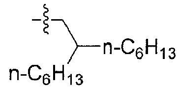

43 S S S O(n-C6H13) O(n-C6H13) 44 Se Se Se n-C6H13 n-C6H13 46 S S S O(n-C7H15) O(n-C7H15) 47 S S S O(n-C8H17) O(n-C8H17) 48 S S S O(n-C9H19) O(n-C9H19) 49 S S S O(n-C10H21) O(n-C10H21) Dashed line indicates a chemical bond. -

Table 3 Compound No. E1 E2 E3 R1 R2 51 S S S O(n-C11H23) O(n-C11H23) 52 S S S O(n-C12H25) O(n-C12H25) 53 S S S O(n-C13H27) O(n-C13H27) 54 S S S O(n-C14H29) O(n-C14H29) 55 S S S O(n-C15H31) O(n-C15H31) 56 S S S O(n-C16H33) O(n-C16H33) 57 S S S O(n-C17H35) O(n-C17H35) 58 S S S O(n-C18H37) O(n-C18H37) 59 S S S O(n-C19H39) O(n-C19H39) 60 S S S O(n-C20H41) O(n-C20H41) 61 S S S O(n-C21H43) O(n-C21H43) 62 S S S O(n-C22H45) O(n-C22H45) 63 S S S O(n-C23H47) O(n-C23H47) 64 S S S O(n-C24H49) O(n-C24H49) 65 S S S O(n-C25H51) O(n-C25H51) 66 S S S O(n-C26H53) O(n-C26H53) 67 S S S O(n-C27H55) O(n-C27H55) 68 S S S O(n-C28H57) O(n-C28H57) 69 S S S O(n-C29H59) O(n-C29H59) 70 S S S O(n-C30H61) O(n-C30H61) 71 S S S O(n-C6F13) O(n-C6F13) 72 S S S O(n-C8F17) O(n-C8F17) 73 S S S O(n-C12F25) O(n-C12F25) 74 S Se S O(n-C6H13) O(n-C6H13) 75 Se S Se O(n-C8H17) O(n-C8H17) 76 S S S O(n-C8H17) H 77 S S S O(n-C8H17) O(n-C12H25) 78 S S S 

79 S S S 

Dashed line indicates a chemical bond. -
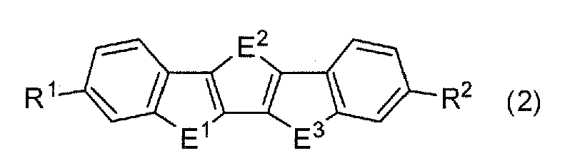
Table 4 Compound No. E1 E2 E3 R1 R2 80 S S S 

81 S S S 

82 S S S 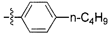

84 S S S 

86 S S S 

87 S S S 

89 S S S 

90 S S S 

91 S S S 

93 S S S 

94 S S S 

95 S S S 

Dashed line indicates a chemical bond. -

Table 5 Compound No. E1 E2 E3 R1 R2 96 S S S 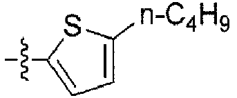

97 S S S 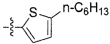

99 S S S 

100 S S S 

102 S S S 
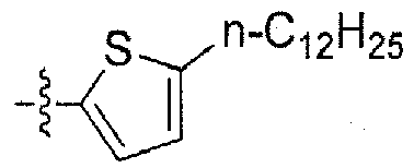
103 S S S 

104 S S S 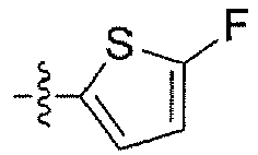

105 S S S 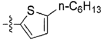
H 106 S S S 

107 S Se S 

108 S S S 

Dashed line indicates a chemical bond. -

Table 6 Compound No. E1 E2 E3 R1 R2 114 S S S 

117 S S S 

118 S S S 

119 S S S 

120 S S S 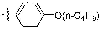
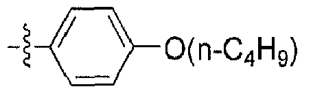
122 S S S 

124 S S S 

Dashed line indicates a chemical bond. -

Table 7 Compound No. E1 E2 E3 R1 R2 125 S S S 

127 S S S 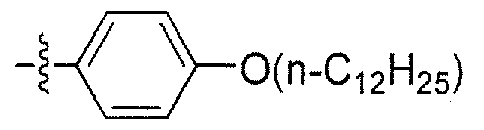

128 S S S 

129 S S S 

131 S S S 

132 S S S 

133 S S S 

135 S S S 

136 S S S 

138 S S S 

139 S S S 

Dashed line indicates a chemical bond. -

Table 8 Compound No. E1 E2 E3 R1 R2 140 S Se S 
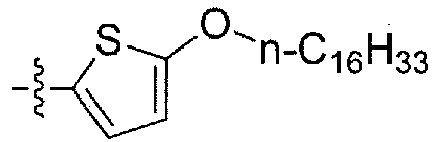
141 Se S Se 
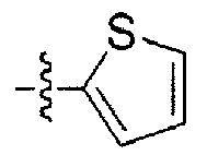
142 S S S 

143 S Se S 

144 S S S 

145 S S S -Si(CH3)2(n-C8H17) -Si(CH3)2(n-C8H17) 146 S S S -Si(CH3)2(n-C10H21) -Si(CH3)2(n-C10H21) Dashed line indicates a chemical bond. -

Table 9 Compound No. E1 E2 E3 R1 R2 152 S S S 

153 S S S 

154 S S S 

155 S S S 

156 S S S 

157 S S S 

158 S S S 

159 S S S 

160 S S S 

161 S S S 

162 S S S 

163 S S S 

164 S S S 

165 S S S 

Dashed line indicates a chemical bond. -

Table 10-1 Compound No. E1 E2 E3 R1 R2 166 S S S 
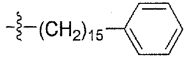
167 S S S 

168 S S S 

169 S S S 
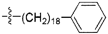
170 S S S 

171 S S S 

172 S S S 

173 S S S 

174 S S S 

175 S S S 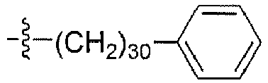

Dashed line indicates a chemical bond. 
Table 10-2 Compound No. E1 E2 E3 R1 R2 176 S S S 

177 S S S 

178 S S S 

179 Se Se Se 
n-C6H13 180 S S S 

181 S S S 

182 S Se S 
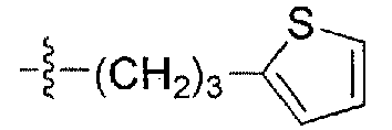
183 S Se S 

184 S Se S 

Dashed line indicates a chemical bond. -

Table 11-1 Compound No. E1 E2 E3 R1 R2 185 S S S 

186 S S S 

187 S S S 

188 S S S 
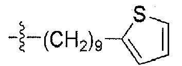
189 S S S 

190 S S S 

191 S S S 

192 S S S 

193 S S S 

194 S S S 

Dashed line indicates a chemical bond. 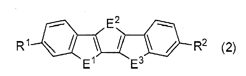
Table 11-2 Compound No. E1 E2 E3 R1 R2 195 S S S 

196 S S S 

197 S S S 

198 S S S 

199 S S S 

200 S S S 

201 S S S 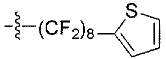

202 S S S 

203 S S S 
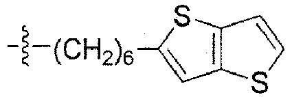
Dashed line indicates a chemical bond. -

Table 12 Compound No. E1 E2 E3 R1 R2 204 S S S 

205 S S S 
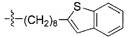
206 Se Se Se 

207 S S S 

208 S S S -Si(CH3)3 -Si(CH3)3 209 S S S -Si(C2H5)3 -Si(C2H5)3 210 S S S -Si(i-C3H7)3 -Si(i-C3H7)3 211 S S S -Si(CH3)2(t-C4H9) -Si(CH3)2(t-C4H9) 212 S S S -Si(CH3)2(n-C6H13) -Si(CH3)2(n-C6H13) 213 S S S -Si(CH3)2(n-C12H25) -Si(CH3)2(n-C12H25) Dashed line indicates a chemical bond. -

Table 13 Compound No. E1 E2 E3 R1 R2 214 S S S n-C4H9 n-C4H9 215 S S S s-C4H9 s-C4H9 216 S S S n-C5H11 n-C5H11 217 S S S 

218 S S S n-C6H13 n-C6H13 219 S S S 

220 S S S 

221 S S S n-C7H15 n-C7H15 222 S S S n-C8H17 n-C8H17 223 S S S n-C9H19 n-C9H19 224 S S S n-C10H21 n-C10H21 Dashed line indicates a chemical bond. -

Table 14 Compound No. E1 E2 E3 R1 R2 225 S S S 

226 S S S n-C11H23 n-C11H23 227 S S S n-C12H25 n-C12H25 228 S S S n-C13H27 n-C13H27 229 S S S n-C14H29 n-C14H29 230 S S S n-C15H31 n-C15H31 231 S S S n-C16H33 n-C16H33 232 S S S n-C17H35 n-C17H35 233 S S S n-C18H37 n-C18H37 234 S S S n-C19H39 n-C19H39 235 S S S n-C20H41 n-C20H41 236 S S S n-C21H43 n-C21H43 237 S S S n-C22H45 n-C22H45 238 S S S n-C23H47 n-C23H47 239 S S S n-C24H49 n-C24H49 240 S S S n-C25H51 n-C25H51 241 S S S n-C26H53 n-C26H53 242 S S S n-C27H55 n-C27H55 243 S S S n-C28H57 n-C28H57 244 S S S n-C29H59 n-C29H59 245 S S S n-C30H61 n-C30H61 246 S S S n-C6F13 n-C6F13 247 S S S n-C8F17 n-C8F17 248 S S S n-C12F25 n-C12F25 249 S S S n-C16F33 n-C16F33 250 S Se S n-C6H13 n-C6H13 251 Se S Se n-C8H17 n-C8H17 252 S S S n-C8H17 H 253 S S S O(n-C4H9) O(n-C4H9) 254 S S S O(n-C5H11) O(n-C5H11) Dashed line indicates a chemical bond. -

Table 15 Compound No. E1 E2 E3 R1 R2 256 S S S O(n-C6H13) O(n-C6H13) 259 S S S O(n-C7H15) O(n-C7H15) 260 S S S O(n-C8H17) O(n-C8H17) 261 S S S O(n-C9H19) O(n-C9H19) 262 S S S O(n-C10H21) O(n-C10H21) 264 S S S O(n-C11H23) O(n-C11H23) 265 S S S O(n-C12H25) O(n-C12H25) 266 S S S O(n-C13H27) O(n-C13H27) 267 S S S O(n-C14H29) O(n-C14H29) 268 S S S O(n-C15H31) O(n-C15H31) 269 S S S O(n-C16H33) O(n-C16H33) 270 S S S O(n-C17H35) O(n-C17H35) 271 S S S O(n-C18H37) O(n-C18H37) 272 S S S O(n-C19H39) O(n-C19H39) 273 S S S O(n-C20H41) O(n-C20H41) 274 S S S O(n-C21H43) O(n-C21H43) 275 S S S O(n-C22H45) O(n-C22H45) 276 S S S O(n-C23H47) O(n-C23H47) 277 S S S O(n-C24H49) O(n-C24H49) 278 S S S O(n-C25H51) O(n-C25H51) 279 S S S O(n-C26H53) O(n-C26H53) 280 S S S O(n-C27H55) O(n-C27H55) 281 S S S O(n-C28H57) O(n-C28H57) 282 S S S O(n-C29H59) O(n-C29H59) 283 S S S O(n-C30H61) O(n-C30H61) 284 S S S O(n-C6F13) O(n-C6F13) 285 S S S O(n-C8F17) O(n-C8F17) 286 S S S O(n-C12F25) O(n-C12F25) 287 S S S O(n-C16F33) O(n-C16F33) 288 S Se S O(n-C6H13) O(n-C6H13) 289 Se S Se O(n-C8H17) O(n-C8H17) Dashed line indicates a chemical bond. -

Table 16 Compound No. E1 E2 E3 R1 R2 290 S S S O(n-C8H17) O(n-C12H25) 291 S S S 
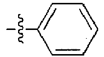
292 S S S 

293 S S S 

294 S S S 

295 S S S 

297 S S S 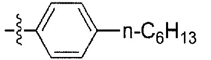

299 S S S 

300 S S S 

302 S S S 

303 S S S 

304 S S S 

Dashed line indicates a chemical bond. -

Table 17 Compound No. E1 E2 E3 R1 R2 306 S S S 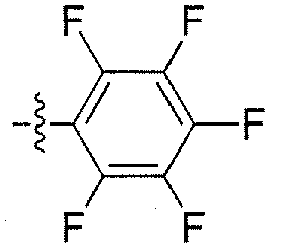

307 S S S 
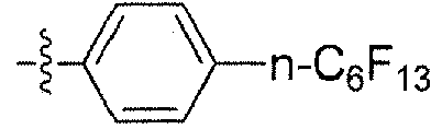
308 S S S 

309 S S S 

310 S S S 

312 S S S 

313 S S S 

315 S S S 

316 S S S 

317 S S S 

318 S S S 

319 S S S 

320 S Se S 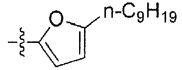

Dashed line indicates a chemical bond. -

Table 18 Compound No. E1 E2 E3 R1 R2 321 S S S 

327 S S S 

330 S S S 

331 S S S 

332 S S S 

333 S S S 

335 S S S 

Dashed line indicates a chemical bond. -

Table 19 Compound No. E1 E2 E3 R1 R2 337 S S S 

338 S S S 

340 S S S 

341 S S S 

342 S S S 

344 S S S 

345 S S S 

346 S S S 

348 S S S 

349 S S S 

Dashed line indicates a chemical bond. -

Table 20 Compound No. E1 E2 E3 R1 R2 351 S S S 

352 S S S 

353 S Se S 

354 Se S Se 

355 S S S 

356 S Se S 

357 S S S 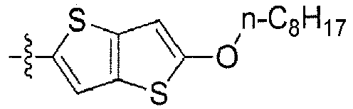
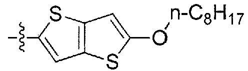
Dashed line indicates a chemical bond. -
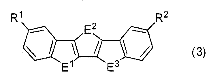
Table 21 Compound No. E1 E2 E3 R1 R2 365 S S S 

366 S S S 

367 S S S 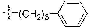

368 S S S 

369 S S S 

370 S S S 

371 S S S 

372 S S S 

373 S S S 

374 S S S 

375 S S S 

376 S Se S 

377 S S S 

378 S S S 

379 S S S 

380 Se S Se 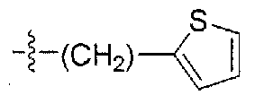

381 S S S 

Dashed line indicates a chemical bond. -

Table 22 Compound No. E1 E2 E3 R1 R2 382 S S S 

383 S Se S 

384 S S S 

385 S S S 

386 S S S 

387 S S S 

388 S S S 

389 S S S 

390 S S S 

391 S S S 

392 S S S 

393 Se Se Se 

394 S S S -Si(CH3)3 -Si(CH3)3 395 S S S -Si(C2H5)3 -Si(C2Hs)3 396 S S S -Si(i-C3H7)3 -Si(i-C3H7)3 397 S S S -Si(CH3)2(t-C4H9) -Si(CH3)2(t-C4H9) 398 S S S -Si(CH3)2(n-C6H13) -Si(CH3)2(n-C6H13) 399 S S S -Si(CH3)2(n-C12H25) -Si(CH3)2(n-C12H25) Dashed line indicates a chemical bond. -

Table 23 Compound No. E1 E2 E3 R1 R2 400 S S S n-C4H9 n-C4H9 401 S S S n-C5H11 n-C5H11 402 S S S 

403 S S S n-C6H13 n-C6H13 404 S S S 

405 S S S 
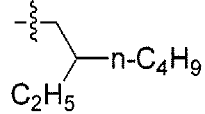
406 S S S n-C8H17 n-C8H17 407 S S S 

408 S S S n-C12H25 n-C12H25 409 S S S n-C13H27 n-C13H27 410 S S S n-C16H33 n-C16H33 411 S S S n-C18H37 n-C18H37 412 S S S n-C20H41 n-C20H41 413 S S S n-C25H51 n-C25H51 414 S S S n-C30H61 n-C30H61 415 S S S n-C6F13 n-C6F13 416 S Se S n-C6H13 n-C6H13 417 Se S Se n-C8H17 n-C8H17 418 S S S n-C6H13 n-C12H25 420 S S S O(n-C6H13) O(n-C6H13) 423 S S S O(n-C8H17) O(n-C8H17) 425 S S S O(n-C12H25) O(n-C12H25) Dashed line indicates a chemical bond. -

Table 24 Compound No. E1 E2 E3 R1 R2 426 S S S O(n-C8F17) O(n-C8F17) 427 S Se S O(n-C6H13) O(n-C6H13) 428 S S S O(n-C8H17) O(n-C12H25) 429 S S S 

431 S S S 

433 S S S 

434 S S S 

436 S S S 
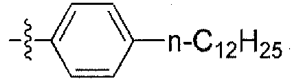
437 S S S 

439 S S S 

440 S S S 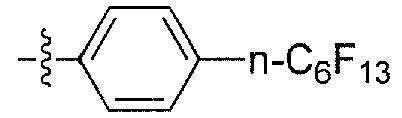

441 S S S 
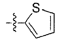
Dashed line indicates a chemical bond. -

Table 25 Compound No. E1 E2 E3 R1 R2 442 S S S 

443 S S S 

445 S S S 

446 S S S 

448 S S S 

449 S S S 

450 S S S 

451 S S S 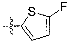

452 S S S 

456 S S S 

Dashed line indicates a chemical bond. -

Table 26 Compound No. E1 E2 E3 R1 R2 459 S S S 

461 S S S 

463 S S S 
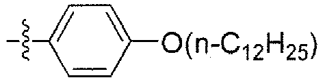
464 S S S 

466 S S S 

467 S S S 
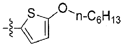
469 S S S 

470 S S S 

Dashed line indicates a chemical bond. -

Table 27 Compound No. E1 E2 E3 R1 R2 472 S S S 

473 S S S 

474 S Se S 

475 S S S 

479 S S S 

480 S S S 

481 S S S 

482 S S S 

483 S S S 

484 S S S 
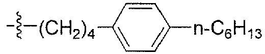
485 S S S 

Dashed line indicates a chemical bond. -

Table 28 Compound No. E1 E2 E3 R1 R2 486 Se S Se 

487 S S S 

488 S S S 

489 S S S 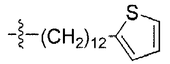

490 S S S 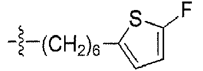

491 S S S 

492 S S S 

493 S S S 

494 S S S 

495 S S S 

496 S S S -Si(CH3)3 -Si(CH3)3 Dashed line indicates a chemical bond. -

Table 29 Compound No. E1 E2 E3 R1 R2 497 S S S n-C6H13 n-C6H13 498 S S S n-C12H25 n-C12H25 499 S S S n-C13H27 n-C13H27 500 S S S n-C6F13 n-C6F13 501 S S S O(n-C6H13) O(n-C6H13) 502 S S S 

503 S S S 

504 S S S 

505 S S S 

509 S S S 

513 S S S 

514 S S S 

Dashed line indicates a chemical bond. -

Table 30 Compound No. E1 E2 E3 R1 R2 515 Se S Se 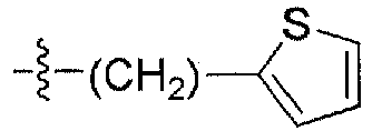

516 S S S 

517 S S S 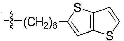

518 S S S 

519 S S S 

520 S S S -Si(CH3)3 -Si(CH3)3 Dashed line indicates a chemical bond. -

Table 31 Compound No. E1 E2 E3 R1 R2 521 S S S n-C6H13 n-C6H13 522 S S S O(n-C6H13) O(n-C6H13) 523 S S S 

524 S S S 

Dashed line indicates a chemical bond. -

Table 32 Compound No. E1 E2 E3 R1 R2 530 S S S 

531 S S S 
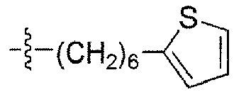
532 S S S 

533 S S S 

534 S S S -Si(CH3)3 -Si(CH3)3 Dashed line indicates a chemical bond. -

Table 33 Compound No. E1 E2 E3 R1 R2 535 S S S n-C6H13 n-C6H13) 536 S S S O(n-C6H13) O(n-C6H13) 537 S S S 
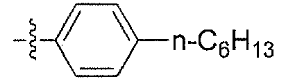
538 S S S 

Dashed line indicates a chemical bond. -

Table 34 Compound No. E1 E2 E3 R1 R2 545 S S S 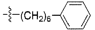

546 S S S 

547 S S S 

548 S S S 

549 S S S -Si(CH3)3 -Si(CH3)3 Dashed line indicates a chemical bond. -

Table 35 Compound No. E1 E2 E3 R1 R2 550 S S S n-C6H13 n-C6H13 551 S S S 

554 S S S 

555 S S S 

556 S S S -Si(CH3)3 -Si(CH3)3 Dashed line indicates a chemical bond. -

Table 36 Compound No. E1 E2 E3 R1 R2 557 S S S n-C6H13 n-C6H13 558 S S S 

561 S S S 

562 S S S 

563 S S S -Si(CH3)3 -Si(CH3)3 Dashed line indicates a chemical bond. -

Table 37 Compound No. E1 E2 E3 R1 R2 564 S S S n-C6H13 n-C6H13 565 S S S 

568 S S S 

569 S S S 

570 S S S -Si(CH3)3 -Si(CH3)3 Dashed line indicates a chemical bond. - Among the substituted benzochalcogenoacene compounds (1), a compound is preferable in which three of E's in the benzochalcogenoacene compound (1) are all sulfur atoms.
Especially, the substituted benzochalcogenoacene compounds (1) having the following numbers in the above tables are preferably exemplified: - 1, 3, 4, 5, 6, 7, 8, 9, 10, 11, 12, 13, 14, 15, 16, 17, 18, 19, 20, 21, 22, 33, 34, 35, 38, 39, 40, 41, 42, 43, 44, 46, 47, 48, 49, 51, 52, 53, 54, 55, 56, 57, 58, 59, 60, 76, 77, 78, 79, 80, 81, 82, 84, 86, 87, 89, 90, 91, 94, 95, 96, 97, 99, 100, 102, 103, 104, 105, 106, 108, 117, 118, 119, 120, 122, 124, 125, 127, 128, 129, 131, 132, 133, 135, 136, 138, 139, 142, 144, 152, 153, 154, 155, 156, 157, 158, 159, 160, 161, 162, 163, 164, 165, 166, 167, 168, 169, 170, 176, 180, 181, 182, 183, 184, 185, 186, 187, 188, 189, 202, 203, 204, 205, 206; 208, 209, 210, 211, 212, 213, 214, 215, 216, 217, 218, 219,220, 221, 222, 223, 224, 225, 226, 227, 228, 229, 230, 231, 232, 233, 234, 235, 246, 247, 248, 252, 253, 254, 256, 259, 260, 261, 262, 264, 265, 266, 267, 268, 269, 270, 271, 272, 273, 284, 285, 286, 291, 292, 293, 294, 295, 297, 299, 300, 302, 306, 307, 308, 309, 310, 312, 313, 315, 3I6, 317, 319, 321, 327, 330, 331, 332, 333, 335, 337, 338, 340, 341, 342, 344, 345, 346, 348, 349, 351, 352, 353, 354, 357, 365, 366, 367, 368, 369, 370, 371, 372, 373, 374, 375, 379, 380, 381, 382, 383, 384, 385, 386, 387, 388, 389, 390, 391, 392, 393, 394, 395, 396, 397, 398 and 399.
- The substituted benzochalcogenoacene compounds (1) having the following numbers in the above tables are exemplified as more preferable:
- 1, 3, 4, 5, 6, 7, 8, 9, 10, 11, 12, 15, 16, 17, 18, 38, 39, 40, 41, 42, 43, 46, 47, 48, 49, 51, 52, 53, 54, 55, 56, 76, 78, 80, 81, 82, 84, 86, 87, 89, 90, 91, 95, 96, 97, 99, 100, 102, 103, 108, 118, 119, 120, 122, 124, 125, 127, 128, 129, 132, 133, 135, 136, 138, 139, 144, 152, 153, 154, 155, 156, 157, 158, 159, 160, 161, 176, 180, 181, 182, 183, 184, 185, 186, 187, 188, 189, 202, 203, 205, 206, 208, 209, 211, 214, 215, 216, 217, 218, 219, 220, 221, 222, 223, 224, 225, 226, 227, 228, 229, 230, 231, 252, 253, 254, 256, 259, 260, 261, 262, 264, 265, 266, 267, 268, 269, 291, 293, 294, 295, 297, 299, 300, 302, 308, 309, 310, 312, 313, 315, 316, 317, 321, 327, 330, 331, 332, 333, 335, 337, 338, 340, 341, 344, 345, 346, 348, 349, 351, 352, 353, 354, 357, 365, 366, 367, 368, 369, 370, 371, 380, 381, 382, 383, 384, 385, 386, 389, 390, 392, 394, 395, 396 and 397.
- The substituted benzochalcogenoacene compound (1) of the present invention is excellent in the solubility in the organic solvent, therefore, its handling is easy and its purification is easily carried out.
A thin film can be also formed by dissolving the substituted benzochalcogenoacene compound (1) in the organic solvent, applying the solution and drying it. The thin film can be easily formed by the applying and film-forming process to be described hereinafter, since the substituted benzochalcogenoacene compound (1) is excellent in the solubility.
In addition, the substituted benzochalcogenoacene compound (1) can provide a thin film showing high carrier mobility. - A process for producing the substituted benzochalcogenoacene compound (1) is described below.
In the process for producing the compound (1), firstly a diacetylene compound is provided which is represented, for example, by the formula (5-1) (hereinafter optionally described as a "compound (5-1)"):

Then, a mixture of the obtained compound (4-1) and a platinum compound such as biscyclooctadienyl platinum (Pt(COD)2) or a copper compound such as a copper powder is heated in the absence of a solvent (hereinafter, optionally described as a "3rd-1 reaction"), or a mixture of the obtained compound (4-1), a nickel compound such as biscyclooctadienyl nickel (Ni(COD)2) and a phosphine compound is heated and stirred in the presence of a solvent (optionally described as a "3rd-2 reaction"). - The organometallic bases used in the present 1st reaction are exemplified by organolithium compounds such as methyllithium (MeLi), n-butyllithium (n-BuLi), sec-butyllithium (sec-BuLi) and tert-butyllithium (t-BuLi) and an organomagnesium compound such as an alkylgrignard compound. From the view point of a better reactivity in the halogen-metal exchange reaction, the organolithium compound is preferable as the organometallic base. For example, butyllithium (BuLi) can be used, and more preferably, t-butyl lithium (t-BuLi) can be used. (An expression in equivalent tends to be understood as unclear. Therefore, an expression based on the amount (moles) of the compound is also described side by side as below.)
The amount of the organometallic base to be used based on 1 mole of the compound (5-1) is, for example, in the range of 4 to 20 moles (in the range of 2 to 10 equivalents to 1 equivalent of a halogen atom), preferably in the range of 6 to 14 moles (in the range of 3 to 7 equivalents to 1 equivalent of a halogen atom), more preferably, in the range of 7 to 10 moles (in the range of 3.5 to 5 equivalents to 1 equivalent of the halogen atom). When the amount of the organometallic base used is 4 moles or more, the unreacted amount of the compound (5-1) is reduced and the yield of the obtained compound (4-1) tends to increase. When the amount used is 20 moles or less, a progress of a side reaction is suppressed and a purification of the compound (4-1) tends to become easy. - The present 1st reaction and the succeeding 2nd reaction are preferable to be carried out in the presence of a solvent.
The solvent used is selected from those which do not remarkably prevent the present 1st and 2nd reactions. For example, aliphatic hydrocarbon solvents such as pentane, hexane and heptane, aromatic solvents such as benzene, toluene and xylene, ether solvents such as diethyl ether and tetrahydrofuran (THF) and the mixtures of 2 or more selected among them are used. A preferable solvent is the ether solvent. - The present 1st reaction is carried out at temperatures of, for example, -20°C or lower, preferably, -40°C or lower, more preferably, -60°C or lower. The reaction time of the present 1st reaction can be controlled by the kind of organometallic bases or the solvents or by the reaction temperature, and the reaction time is in the range around from 10 minutes to 5 hours. Following the present 1st reaction, the present second reaction is carried out. A sulfur (or selenium) may be used as purchased or may be added as a solution or a suspension dissolved or suspended in the solvent used in the present 1st reaction. After addition of the sulfur (or selenium), the reaction temperature may be kept at a similar temperature to the present 1st reaction or may be heated in the temperature range which does not exceed the boiling point of the solvent used. Preferably, heating is carried out to reach the temperature range of 0 to 40°C, and subsequently, the temperature is kept in the same range. The reaction time is, for example, from 30 minutes to 72 hours.
- A crystalline, powder or colloidal sulfur (or selenium) can be used as the sulfur or selenium to be used in the present 2nd reaction. The amount of the sulfur or selenium used may be, for example, in the range of 4 to 20 moles, preferably, in the range of 6 to 14 moles, more preferably, in the range of 7 to 10 moles based on 1 mole of the compound (1-5). It is preferable to use the sulfur (or selenium) in the amount of 4 moles or more, since the yield of the compound (4-1) tends to increase in the molar range. It is also preferable to use the sulfur (or selenium) in the amount of 20 moles or less, since, in the molar range, a progress of a side reaction can be inhibited and a purification of the compound (4-1) tends to become easy.
- After completing the present 2nd reaction, a solvent in the reaction mixture is optionally evaporated. To the obtained reaction mixture, an alkaline water solution such as a sodium hydroxide water solution or a potassium hydroxide water solution is added, and the obtained compound (4-1) is extracted. When the solvent used in the present 1st and 2nd reactions is water, the solvent can be used directly as an extraction solvent. However, it is preferable to use a halogenated hydrocarbon solvent such as dichloromethane or chloroform as the extraction solvent. After obtaining two phases consisting of an organic phase and a water phase, the water phase is separated, then, to the water phase, a water solution of a hexacyanoferrate (III) salt such as potassium ferrycyanide is added, and subsequently, the compound (4-1) is extracted from the water phase by using an organic solvent such as said extraction solvent. The compound (4-1) thus obtained may be optionally purified further by the processes such as chromatography and recrystallization.
- In the present 3rd-1 reaction, a copper compound or a platinum compound can be used in an amount of, for example, 0.5 to 20 moles, preferably 1 to 10 moles, more preferably 2 to 7 moles based on 1 mole of the compound (4-1). An example of the copper compound is a copper powder and an example of the platinum compound is biscyclooctadienyl platinum (Pt(COD)2).
A reaction temperature of the present 3rd-1 reaction is, for example, from 150 to 400°C, preferably, from 200 to 370°C. A reaction temperature of the present 3rd-1 reaction is within 1 hour, preferably, within 30 minutes. After completing the reaction, the reaction temperature is lowered to room temperature, and insoluble impurities are filtered off by using an organic solvent such as chloroform or dichloromethane which can dissolve the substituted benzochalcogenoacene compound (1). The filtrate is concentrated and optionally followed by application of column chromatography, recrystallization, etc. to result in the production of the substituted benzochalcogenoacene compound (1). - A zero valent nickel compound such as biscyclooctadienyl nickel (Ni(COD)2) is preferable as a nickel compound used in the present 3rd-1 reaction. The zero valent nickel compound may be formed in-situ by reduction of a two valent nickel compound such as bisacetylacetonato nickel (Ni(acac)2) with a reducing agent such as diisobutylaluminum hydride.
The amount of the nickel compound used is, for example, in a range of 0.5-5 moles, and preferably in a range of 0.7-3 moles based on 1 mole of the compound (4-1).
Examples of a phosphine compound include triphenylphosphine, tricyclohexylphosphine, tri(o-tolyl)phosphine, trimethylphosphine, tri-t-butylphosphine, 1,2-(diphenylphosphino)ethane, 1,3-(diphenylphosphino)propane, 1,4-(diphenylphosphino)butane and 1,1-bis(diphenylphosphino)ferrocene. Among them, triphenylphosphine is preferable.
The amount of the phosphine compound used is, for example, in a range of 0.5-20 moles of the phosphine compound, preferably, in a range of 0.7-10 moles based on 1 mole of the nickel compound. - Examples of a solvent used in the present 3rd-2 reaction include an aliphatic hydrocarbon solvent such as pentane, hexane and heptane, an aromatic hydrocarbon solvent such as benzene, toluene and xylene, and a halogenated hydrocarbon solvent such as dichloromethane and chloroform. These solvents can be use alone or in a mixture of 2 or more of them. The aromatic hydrocarbon solvent is preferable, and toluene is more preferable as the solvent.
The reaction temperature of the present 3rd-2 reaction is, for example, in a range from 10°C to a boiling point or lower of the solvent.
The reaction time of the present 3rd-2 reaction is preferably within 72 hours depending on the reaction temperature.
After completing the present 3rd-2 reaction, insoluble impurities are filtered off optionally under heating. The filtrate is concentrated and optionally followed by purification using column chromatography, recrystallization, etc. to result in the production of the substituted benzochalcogenoacene compound (1). - Specific examples of the compound (5-1) used in the present 1st reaction are described in the following tables.
Table 38 
Compound No. X1 X2 R1 R2 1141 Br Br n-C4H9 n-C4H9 1142 Br Br S-C4H9 s-C4H9 1143 Br Br n-C5H11 n-C5H11 1144 Br Br 

1145 Br Br n-C6H13 n-C6H13 1146 Br Br 

1147 Br Br 

1148 Br Br n-C7H15 n-C7H15 1149 Br Br n-C8H17 n-C8H17 1150 Br Br n-C9H19 n-C9H19 1151 Br Br n-C10H21 n-C10H21 1152 Br Br 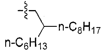

1153 Br Br n-C11H23 n-C11H23 1154 Br Br n-C12H25 n-C12H25 1155 Br Br n-C13H27 n-C13H27 Dashed line indicates a chemical bond. -
Table 39 
Compound No. X1 X2 R1 R2 1156 Br Br n-C14H29 n-C14H29 1157 Br Br n-C15H31 n-C15H31 1158 Br Br n-C16H33 n-C16H33 1159 Br Br n-C17H35 n-C17H35 1160 Br Br n-C18H37 n-C18H37 1161 Br Br n-C19H39 n-C19H39 1162 Br Br n-C20H41 n-C20H41 1163 Br Br n-C21H43 n-C21H43 1164 Br Br n-C22H45 n-C22H45 1165 Br Br n-C23H47 n-C23H47 1166 Br Br n-C24H49 n-C24H49 1167 Br Br n-C25H51 n-C25H51 1168 Br Br n-C26H53 n-C26H53 1169 Br Br n-C27H55 n-C27H55 1170 Br Br n-C28H57 n-C28H57 1171 Br Br n-C29H59 n-C29H59 1172 Br Br n-C30H61 n-C30H61 1173 Br Br n-C6F13 n-C6F13 1174 Br Br n-C8F17 n-C8F17 1175 Br Br n-C12F25 n-C12F25 1176 Br Br n-C16F33 n-C16F33 1177 I I n-C6H13 n-C6H13 1178 Br Br n-C8H17 H 1179 Br Br n-C6H13 n-C12H25 1180 Br Br O(n-C4H9) O(n-C4H9) 1181 Br Br O(n-C5H11) O(n-C5H11) 1183 Br Br O(n-C6H13) O(n-C6H13) 1186 Br Br O(n-C7H15) O(n-C7H15) 1187 Br Br O(n-C8H17) O(n-C8H17) 1188 Br Br O(n-C9H19) O(n-C9H19) 1189 Br Br O(n-C10H21) O(n-C10H21) Dashed line indicates a chemical bond. -
Table 40 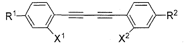
Compound No. X1 X2 R1 R2 1191 Br Br O(n-C11H23) O(n-G11H23) 1192 Br Br O(n-C12H25) O(n-C12H25) 1193 Br Br O(n-C13H27) O(n-C13H27) 1194 Br Br O(n-C14H29) O(n-C14H29) 1195 Br Br O(n-C15H31) O(n-C15H31) 1196 Br Br O(n-C16H33) O(n-C16H33) 1197 Br Br O(n-C17H35) O(n-C17H35) 1198 Br Br O(n-C18H37) O(n-C18H37) 1199 Br Br O(n-C19H39) O(n-C19H39) 1200 Br Br O(n-C20H41) O(n-C20H41) 1201 Br Br O(n-C21H43) O(n-C21H43) 1202 Br Br O(n-C22H45) O(n-C22H45) 1203 Br Br O(n-C23H47) O(n-C23H47) 1204 Br Br O(n-C24H49) O(n-C24H49) 1205 Br Br O(n-C25H51) O(n-C25H51) 1206 Br Br O(n-C26H53) O(n-C26H53) 1207 Br Br O(n-C27H55) O(n-C27H55) 1208 Br Br O(n-C28H57) O(n-C28H57) 1209 Br Br O(n-C29H59) O(n-C29H59) 1210 Br Br O(n-C30H61) O(n-C30H61) 1211 Br Br O(n-C6F13) O(n-C6F13) 1212 Br Br O(n-C8F17) O(n-C8F17) 1213 Br Br O(n-C12F25) O(n-C12F25) 1214 Br Br O(n-C16H13) O(n-C16F33) 1215 Br I O(n-C6H13) O(n-C6H13) 1216 I I O(n-C8H17) O(n-C8H17) 1217 Br Br O(n-C8H17) O(n-C12H25) 1218 Br Br 

1219 Br Br 

Dashed line indicates a chemical bond. -
Table 41 
Compound No. X1 X2 R1 R2 1220 Br Br 

1221 Br Br 

1222 Br Br 

1224 Br Br 

1226 Br Br 

1227 Br Br 

1229 Br Br 
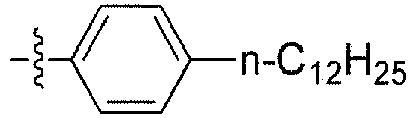
1230 Br Br 

1231 Br Br 

1233 Br Br 

1234 Br Br 

1235 Br Br 

Dashed line indicates a chemical bond. -
Table 42 
Compound No. X1 X2 R1 R2 1236 Br Br 

1237 Br Br 

1239 Br Br 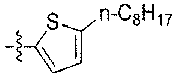
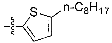
1240 Br Br 

1242 Br Br 

1243 Br Br 

1244 Br Br 

1245 Br Br 

1246 Br Br 

1247 Br Br 

1248 Br Br 

Dashed line indicates a chemical bond. -
Table 43 
Compound No. X1 X2 R1 R2 1254 Br Br 

1257 Br Br 

1258 Br Br 

1259 Br Br 

1260 Br Br 

1262 Br Br 

1264 Br Br 

Dashed line indicates a chemical bond. -
Table 44 
Compound No. X1 X2 R1 R2 1265 Br Br 

1267 Br Br 

1268 Br Br 

1269 Br Br 

1271 Br Br 

1272 Br Br 

1273 Br Br 

1275 Br Br 

1276 Br Br 
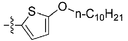
1278 Br Br 

1279 Br Br 

Dashed line indicates a chemical bond. -
Table 45 
Compound No. X1 X2 R1 R2 1280 Br Br 

1281 Br Br 
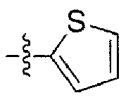
1282 Br Br 

1283 Br Br 

1284 Br Br 

Dashed line indicates a chemical bond. -
Table 46 
Compound No. X1 X2 R1 R2 1292 Br Br 

1293 Br Br 

1294 Br Br 

1295 Br Br 

1296 Br Br 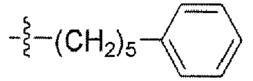

1297 Br Br 

1298 Br Br 

1299 Br Br 

1300 Br Br 

1301 Br Br 

1302 Br Br 

1303 Br Br 

1304 Br Br 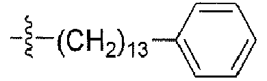

1305 Br Br 

Dashed line indicates a chemical bond. -
Table 47-1 
Compound No. X1 X2 R1 R2 1306 Br Br 

1307 Br Br 

1308 Br Br 
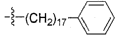
1309 Br Br 

1310 Br Br 

1311 Br Br 

1312 Br Br 

1313 Br Br 
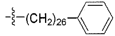
1314 Br Br 

1315 Br Br 

Dashed line indicates a chemical bond. Table 47-2 
Compound No. X1 X2 R1 R2 1316 Br Br 

1317 Br Br 

1318 Br Br 

1319 Br Br 
n-C6H13 1320 Br Br 

1321 Br Br 

1322 Br Br 

1323 Br Br 

1324 Br Br 

Dashed line indicates a chemical bond. -
Table 48-1 
Compound No. X1 X2 R1 R2 1325 Br Br 

1326 Br Br 

1327 Br Br 

1328 Br Br 

1329 Br Br 

1330 Br Br 

1331 Br Br 

1332 Br Br 

1333 Br Br 

1334 Br Br 

Dashed line indicates a chemical bond. Table 48-2 
Compound No. X1 X2 R1 R2 1335 Br Br 

1336 Br Br 

1337 Br Br 

1338 Br Br 

1339 Br Br 

1340 Br Br 

1341 Br Br 

1342 Br Br 

1343 Br Br 

Dashed line indicates a chemical bond. -
Table 49 
Compound No. X1 X2 R1 R2 1344 Br Br 
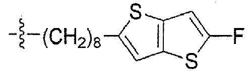
1345 Br Br 

1346 Br Br 

1347 Br Br 

1348 Br Br -Si(CH3)3 -Si(CH3)3 1349 Br Br -Si(C2H5)3 -Si(C2H5)3 1350 Br Br -Si(i-C3H7)3 -Si(i-C3H7)3 1351 Br Br -Si(CH3)2(t-C4H9) -Si(CH3)2(t-C4H9) 1352 Br Br -Si(CH3)2(n-C6H13) -Si(CH3)2(n-C6H13) 1353 Br Br -Si(CH3)2(n-C12H25) -Si(CH3)2(n-C12H25) Dashed line indicates a chemical bond. -
Table 50 
Compound No. X1 X2 R1 R2 1354 Br Br n-C4H9 n-C4H9 1355 Br Br s-C4H9 s-C4H9 1356 Br Br n-C5H11 n-C5H11 1357 Br Br 

1358 Br Br n-C6H13 n-C6H13 1359 Br Br 

1360 Br Br 

1361 Br Br n-C7H15 n-C7H15 1362 Br Br n-C8H17 n-C8H17 1363 Br Br n-C9H19 n-C9H19 1364 Br Br n-C10H21 n-C10H21 Dashed line indicates a chemical bond. -
Table 51 
Compound No. X1 X2 R1 R2 1365 Br Br 

1366 Br Br n-C11H23 n-C11H23 1367 Br Br n-C12H25 n-C12H25 1368 Br Br n-C13H27 n-C13H27 1369 Br Br n-C14H29 n-C14H29 1370 Br Br n-C15H31 n-C15H31 1371 Br Br n-C16H33 n-C16H33 1372 Br Br n-C17H35 n-C17H35 1373 Br Br n-C18H37 n-C18H37 1374 Br Br n-C19H39 n-C19H39 1375 Br Br n-C20H41 n-C20H41 1376 Br Br n-C21H43 n-C21H43 1377 Br Br n-C22H45 n-C22H45 1378 Br Br n-C23H47 n-C23H47 1379 Br Br n-C24H49 n-C24H49 1380 Br Br n-C25H51 n-C25H51 1381 Br Br n-C26H53 n-C26H53 1382 Br Br n-C27H55 n-C27H55 1383 Br Br n-C28H57 n-C28H57 1384 Br Br n-C29H59 n-C29H59 1385 Br Br n-C30H61 n-C30H61 1386 Br Br n-C6F13 n-C6F13 1387 Br Br n-C8F17 n-C8F17 1388 Br Br n-C12F25 n-C12F25 1389 Br Br n-C16F33 n-C16F33 1390 I I n-C6H13 n-C6H13 1391 Br Br n-C8H17 n-C8H17 1392 Br Br n-C6H13 n-C12H25 1393 Br Br O(n-C4H9) O(n-C4H9) 1394 Br Br O(n-C5H11) O(n-C5H11) Dashed line indicates a chemical bond. -
Table 52 
Compound No. X1 X2 R1 R2 1396 Br Br O(n-C6H13) O(n-C6H13) 1399 Br Br O(n-C7H15) O(n-C7H15) 1400 Br Br O(n-C8H17) O(n-C8H17) 1401 Br Br O(n-C9H19) O(n-C9H19) 1402 Br Br O(n-C10H21) O(n-C10H21) 1404 Br Br O(n-C11H23) O(n-C11H23) 1405 Br Br O(n-C12H25) O(n-C12H25) 1406 Br Br O(n-C13H27) O(n-C13H27) 1407 Br Br O(n-C14H29) O(n-C14H29) 1408 Br Br O(n-C15H31) O(n-C15H31) 1409 Br Br O(n-C16H33) O(n-C16H33) 1410 Br Br O(n-C17H35) O(n-C17H35) 1411 Br Br O(n-C18H37) O(n-C18H37) 1412 Br Br O(n-C19H39) O(n-C19H39) 1413 Br Br O(n-C20H41) O(n-C20H41) 1414 Br Br O(n-C21H43) O(n-C21H43) 1415 Br Br O(n-C22H45) O(n-C22H45) 1416 Br Br O(n-C23H47) O(n-C23H47) 1417 Br Br O(n-C24H49) O(n-C24H49) 1418 Br Br O(n-C25H51) O(n-C25H51) 1419 Br Br O(n-C26H53) O(n-C26H53) 1420 Br Br O(n-C27H55) O(n-C27H55) 1421 Br Br O(n-C28H57) O(n-C28H57) 1422 Br Br O(n-C29H59) O(n-C29H59) 1423 Br Br O(n-C30H61) O(n-C30H61) 1424 Br Br O(n-C6F13) O(n-C6F13) 1425 Br Br O(n-C8F17) O(n-C8F17) 1426 Br Br O(n-C12F25) O(n-C12F25) 1427 Br Br O(n-C16F33) O(n-C16F33) 1428 I I O(n-C6H13) O(n-C6H13) 1429 Cl Cl O(n-C8H17) O(n-C8H17) Dashed line indicates a chemical bond. -
Table 53 
Compound No. X1 X2 R1 R2 1430 Br Br O(n-C8H17) O(n-C12H25) 1431 Br Br 

1432 Br Br 

1433 Br Br 

1434 Br Br 
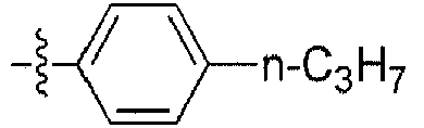
1435 Br Br 

1437 Br Br 

1439 Br Br 

1440 Br Br 

1442 Br Br 

1443 Br Br 

1444 Br Br 

Dashed line indicates a chemical bond. -
Table 54-1 
Compound No. X1 X2 R1 R2 1446 Br Br 

1447 Br Br 

1448 Br Br 

1449 Br Br 

1450 Br Br 

1452 Br Br 

1453 Br Br 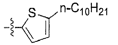

Dashed line indicates a chemical bond. Table 54-2 
Compound No. X1 X2 R1 R2 1455 Br Br 

1456 Br Br 

1457 Br Br 

1458 Br Br 

1459 Br Br 

1460 Br Br 

Dashed line indicates a chemical bond. -
Table 55 
Compound No. X1 X2 R1 R2 1461 Br Br 

1467 Br Br 

1470 Br Br 

1471 Br Br 

1472 Br Br 

1473 Br Br 

1475 Br Br 

Dashed line indicates a chemical bond. -
Table 56 
Compound No. X1 X2 R1 R2 1477 Br Br 
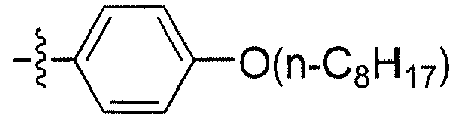
1478 Br Br 

1480 Br Br 

1481 Br Br 
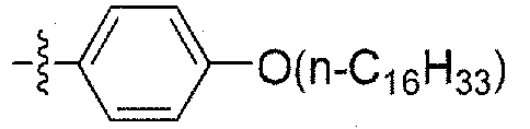
1482 Br Br 

1484 Br Br 

1485 Br Br 

1486 Br Br 

1488 Br Br 

1489 Br Br 

Dashed line indicates a chemical bond. -
Table 57 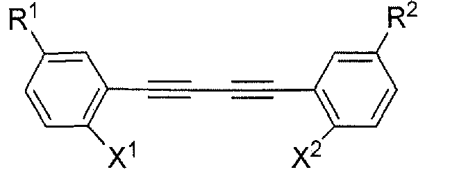
Compound No. X1 X2 R1 R2 1491 Br Br 

1492 Br Br 
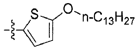
1493 Br Br 

1494 Br Br 

1495 Br Br 

1496 Br Br 

1497 Br Br 

Dashed line indicates a chemical bond. -
Table 58-1 
Compound No. X1 X2 R1 R2 1505 Br Br 

1506 Br Br 

1507 Br Br 

1508 Br Br 

1509 Br Br 

1510 Br Br 
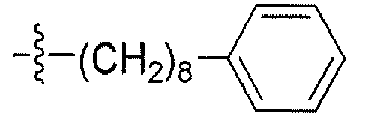
1511 Br Br 

1512 Br Br 

1513 Br Br 

Dashed line indicates a chemical bond. Table 58-2 
Compound No. X1 X2 R1 R2 1514 Br Br 
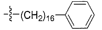
1515 Br Br 

1516 Br Br 

1517 Br Br 

1518 Br Br 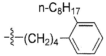

1519 Br Br 

1520 Br Br 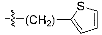

1521 Br Br 

Dashed line indicates a chemical bond. -
Table 59-1 
Compound No. X1 X2 R1 R2 1522 Br Br 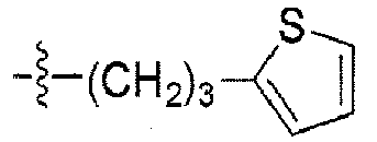

1523 Br Br 

1524 Br Br 

1525 Br Br 

1526 Br Br 

1527 Br Br 

1528 Br Br 

1529 Br Br 

1530 Br Br 

Dashed line indicates a chemical bond. Table 59-2 
Compound No. X1 X2 R1 R2 1531 Br Br 

1532 Br Br 

1533 Br Br 

1534 Br Br -Si(CH3)3 -Si(CH3)3 1535 Br Br -Si(C2Hs)3 -Si(C2Hs)3 1536 Br Br -Si(i-C3H7)3 -Si(i-C3H7)3 1537 Br Br -Si(CH3)2(t-C4H9) -Si(CH3)2(t-C4H9) 1538 Br Br -Si(CH3)2(n-C6H13) -Si(CH3)2(n-C6H13) 1539 Br Br -Si(CH3)2(n-C12H25) -Si(CH3)2(n-C12H25) Dashed line indicates a chemical bond. -
Table 60 
Compound No. X1 X2 R1 R2 1540 Br Br n-C4H9 n-C4H9 1541 Br Br n-C5H11 n-C5H11 1542 Br Br 

1543 Br Br n-C6H13 n-C6H13 1544 Br Br 
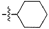
1545 Br Br 

1546 Br Br n-C8H17 n-C8H17 1547 Br Br 

1548 Br Br n-C12H25 n-C12H25 1549 Br Br n-C13H27 n-C13H27 1550 Br Br n-C16H33 n-C16H33 1551 Br Br n-C18H37 n-C18H37 1552 Br Br n-C20H41 n-C20H41 1553 Br Br n-C25H51 n-C25H51 1554 Br Br n-C30H61 n-C30H61 1555 Br Br n-C6F13 n-C6F13 1556 I I n-C6H13 n-C6H13 1557 Cl Cl n-C8H17 n-C8H17 1558 Br Br n-C6H13 n-C12H25 1560 Br Br O(n-C6H13) O(n-C6H13) 1563 Br Br O(n-C8H17) O(n-C8H17) 1565 Br Br O(n-C12H25) O(n-C12H25) Dashed line indicates a chemical bond. -
Table 61 
Compound No. X1 X2 R1 R2 1566 Br Br O(n-C8F17) O(n-C8F17) 1567 I I O(n-C6H13) O(n-C6H13) 1568 Br Br O(n-C8H17) O(n-C12H25) 1569 Br Br 

1571 Br Br 

1573 Br Br 

1574 Br Br 

1576 Br Br 

1577 Br Br 

1579 Br Br 

1580 Br Br 

1581 Br Br 

Dashed line indicates a chemical bond. -
Table 62 
Compound No. X1 X2 R1 R2 1582 Br Br 

1583 Br Br 

1585 Br Br 

1586 Br Br 

1588 Br Br 
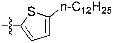
1589 Br Br 

1590 Br Br 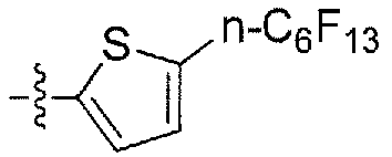

1591 Br Br 

1592 Br Br 
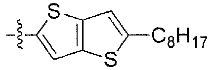
1596 Br Br 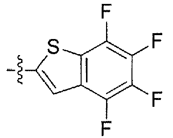

Dashed line indicates a chemical bond. -
Table 63 
Compound No. X1 X2 R1 R2 1599 Br Br 
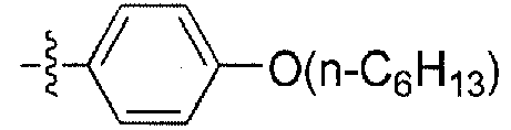
1601 Br Br 
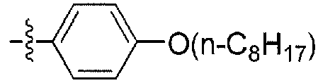
1603 Br Br 

1604 Br Br 

1606 Br Br 

1607 Br Br 

1609 Br Br 

1610 Br Br 

Dashed line indicates a chemical bond. -
Table 64 
Compound No. X1 X2 R1 R2 1612 Br Br 

1613 Br Br 

1614 Br Br 

1615 Br Br 

1619 Br Br 

1620 Br Br 

1621 Br Br 

1622 Br Br 

1623 Br Br 

1624 Br Br 

1625 Br Br 

Dashed line indicates a chemical bond. -
Table 65 
Compound No. X1 X2 R1 R2 1626 Br Br 

1627 Br Br 

1628 Br Br 

1629 Br Br 

1630 Br Br 

1631 Br Br 

1632 Br Br 

1633 Br Br 
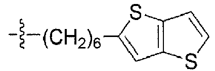
1634 Br Br 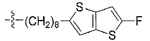

1635 Br Br 

1636 Br Br -Si(CH3)3 -Si(CH3)3 Dashed line indicates a chemical bond. -
Table 66 
Compound No. X1 X2 R1 R2 1637 Br Br n-C6H13 n-C6H13 1638 Br Br n-C12H25 n-C12H25 1639 Br Br n-C13H27 n-C13H27 1640 Br Br n-C6F13 n-C6F13 1641 Br Br O(n-C6H13) O(n-C6H13) 1642 Br Br 

1643 Br Br 

1644 Br Br 

1645 Br Br 

1649 Br Br 

1653 Br Br 

1654 Br Br 

Dashed line indicates a chemical bond. -
Table 67 
Compound No. X1 X2 R1 R2 1655 Br Br 

1656 Br Br 

1657 Br Br 

1658 Br Br 

1659 Br Br 

1660 Br Br -Si(CH3)3 -Si(CH3)3 Dashed line indicates a chemical bond. -
Table 68 
Compound No. X1 X2 R1 R2 1661 Br Br n-C6H13 n-C6H13 1662 Br Br O(n-C6H13) O(n-C6H13) 1663 Br Br 

1664 Br Br 

Dashed line indicates a chemical bond. -
Table 69 
Compound No. X1 X2 R1 R2 1670 Br Br 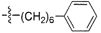

1671 Br Br 

1672 Br Br 

1673 Br Br 

1674 Br Br -Si(CH3)3 -Si(CH3)3 Dashed line indicates a chemical bond. -
Table 70 
Compound No. X1 X2 R1 R2 1675 Br Br n-C6H13 n-C6H13 1676 Br Br O(n-C6H13) O(n-C6H13) 1677 Br Br 

1678 Br Br 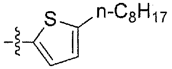

Dashed line indicates a chemical bond. -
Table 71 
Compound No. X1 X2 R1 R2 1685 Br Br 

1686 Br Br 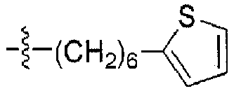

1687 Br Br 

1688 Br Br 

1689 Br Br -Si(CH3)3 -Si(CH3)3 Dashed line indicates a chemical bond. -
Table 72 
Compound No. X1 X2 R1 R2 1690 Br Br n-C6H13 n-C6H13 1691 Br Br 

1694 Br Br 

1695 Br Br 

1696 Br Br -Si(CH3)3 -Si(CH3)3 Dashed line indicates a chemical bond. -
Table 73 
Compound No. X1 X2 R1 R2 1697 Br Br n-C6H13 n-C6H13 1698 Br Br 

1701 Br Br 

1702 Br Br 

1703 Br Br -Si(CH3)3 -Si(CH3)3 Dashed line indicates a chemical bond. -
Table 74 
Compound No. X1 X2 R1 R2 1704 Br Br n-C6H13 n-C6H13 1705 Br Br 

1708 Br Br 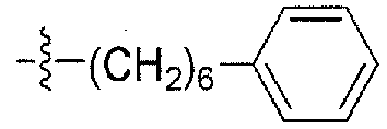
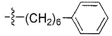
1709 Br Br 

1710 Br Br -Si(CH3)3 -Si(CH3)3 Dashed line indicates a chemical bond. - Specific examples of the compound (4-1) obtained in the present 2nd reaction are illustrated in the following tables.
Table 75 
Compound No. E1 E2 E3 R1 R2 571 S S S n-C4H9 n-C4H9 572 S S S s-C4H9 s-C4H9 573 S S S n-C5H11 n-C5H11 574 S S S 

575 S S S n-C6H13 n-C6H13 576 S S S 

577 S S S 

578 S S S n-C7H15 n-C7H15 579 S S S n-C8H17 n-C8H17 580 S S S n-C9H19 n-C9H19 581 S S S n-C10H21 n-C10H21 582 S S S 

583 S S S n-C11H23 n-C11H23 584 S S S n-C12H25 n-C12H25 585 S S S n-C13H27 n-C13H27 Dashed line indicates a chemical bond. -
Table 76 
Compound No. E1 E2 E3 R1 R2 586 S S S n-C14H29 n-C14H29 587 S S S n-C15H31 n-C15H31 588 S S S n-C16H33 n-C16H33 589 S S S n-C17H35 n-C17H35 590 S S S n-C18H37 n-C18H37 591 S S S n-C19H39 n-C19H39 592 S S S n-C20H41 n-C20H41 593 S S S n-C21H43 n-C21H43 594 S S S n-C22H45 n-C22H45 595 S S S n-C23H47 n-C23H47 596 S S S n-C24H49 n-C24H49 597 S S S n-C25H51 n-C25H51 598 S S S n-C26H53 n-C26H53 599 S S S n-C27H55 n-C27H55 600 S S S n-C28H57 n-C28H57 601 S S S n-C29H59 n-C29H59 602 S S S n-C30H61 n-C30H61 603 S S S n-C6F13 n-C6F13 604 S S S n-C8F17 n-C8F17 605 S S S n-C12F25 n-C12F25 606 S S S n-C6H13 H 607 S Se S n-C6H13 n-C6H13 608 Se S Se n-C8H17 n-C8H17 609 S S S n-C6H13 n-C12H25 610 S S S O(n-C4H9) O(n-C4H9) 611 S S S O(n-C5H11) O(n-C5H11) 613 S S S O(n-C6H13) O(n-C6H13) 616 S S S O(n-C7H15) O(n-C7H15) 617 S S S O(n-C8H17) O(n-C8H17) 618 S S S O(n-C9H19) O(n-C9H19) 619 S S S O(n-C10H21) O(n-C10H21) Dashed line indicates a chemical bond. -
Table 77 
Compound No. E1 E2 E3 R1 R2 621 S S S O(n-C11H23) O(n-C11H23) 622 S S S O(n-C12H25) 0(n-C12H25) 623 S S S O(n-C13H27) O(n-C13H27) 624 S S S O(n-C14H29) O(n-C14H29) 625 S S S O(n-C15H31) O(n-C15H31) 626 S S S O(n-C16H33) O(n-C16H33) 627 S S S O(n-C17H35) O(n-C17H35) 628 S S S O(n-C18H37) O(n-C18H37) 629 S S S O(n-C19H39) O(n-C19H39) 630 S S S O(n-C20H41) O(n-C20H41) 631 S S S O(n-C21H43) O(n-C21H43) 632 S S S O(n-C22H45) O(n-C22H45) 633 S S S O(n-C23H47) O(n-C23H47) 634 S S S O(n-C24H49) O(n-C24H49) 635 S S S O(n-C25H51) O(n-C25H51) 636 S S S O(n-C26H53) O(n-C26H53) 637 S S S O(n-C27H55) O(n-C27H55) 638 S S S O(n-C28H57) O(n-C28H57) 639 S S S O(n-C29H59) O(n-C29H59) 640 S S S O(n-C30H61) O(n-C30H61) 641 S S S O(n-C6F13) O(n-C6F13) 642 S S S O(n-C8F17) O(n-C8F17) 643 S S S O(n-C12F25) O(n-C12F25) 644 S S S O(n-C8H17) H 645 S Se S O(n-C6H13) O(n-C6H13) 646 Se S Se O(n-C8H17) O(n-C8H17) 647 S S S O(n-C8H17) O(n-C12H25) 648 S S S 

649 S S S 

Dashed line indicates a chemical bond. -
Table 78 
Compound No. E1 E2 E3 R1 R2 650 S S S 

651 S S S 

652 S S S 

654 S S S 

656 S S S 

657 S S S 

659 S S S 

660 S S S 

661 S S S 

663 S S S 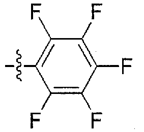

664 S S S 

665 S S S 

Dashed line indicates a chemical bond. -
Table 79 
Compound No. E1 E2 E3 R1 R2 666 S S S 

667 S S S 

669 S S S 

670 S S S 
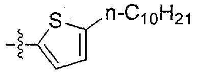
672 S S S 

673 S S S 

674 S S S 

675 S S S 

676 S S S 

677 S Se S 

678 S S S 

Dashed line indicates a chemical bond. -
Table 80 
Compound No. E1 E2 E3 R1 R2 684 S S S 

687 S S S 

688 S S S 

689 S S S 

690 S S S 

692 S S S 

694 S S S 

Dashed line indicates a chemical bond. -
Table 81 
Compound No. E1 E2 E3 R1 R2 695 S S S 

697 S S S 
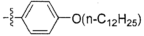
698 S S S 

699 S S S 

701 S S S 

702 S S S 
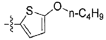
703 S S S 

705 S S S 

706 S S S 

708 S S S 

709 S S S 

Dashed line indicates a chemical bond. -
Table 82 
Compound No. E1 E2 E3 R1 R2 710 S Se S 

711 Se S Se 
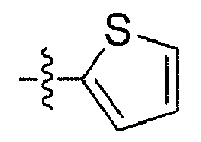
712 S S S 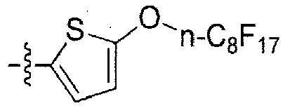

713 S Se S 

714 S S S 

Dashed line indicates a chemical bond. -
Table 83 
Compound No. E1 E2 E3 R1 R2 722 S S S 

723 S S S 

724 S S S 

725 S S S 

726 S S S 

727 S S S 

728 S S S 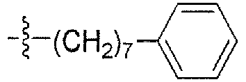

729 S S S 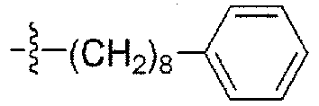

730 S S S 

731 S S S 

732 S S S 

733 S S S 

734 S S S 

735 S S S 

Dashed line indicates a chemical bond. -
Table 84-1 
Compound No. E1 E2 E3 R1 R2 736 S S S 

737 S S S 

738 S S S 

739 S S S 

740 S S S 

741 S S S 
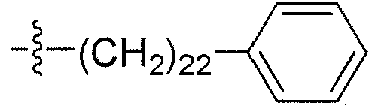
742 S S S 

743 S S S 

744 S S S 

745 S S S 

Dashed line indicates a chemical bond. Table 84-2 
Compound No. E1 E2 E3 R1 R2 746 S S S 

747 S S S 

748 S S S 

749 Se Se Se 
n-C6H13 750 S S S 

751 S S S 

752 S Se S 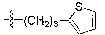

753 S Se S 

754 Se S Se 

Dashed line indicates a chemical bond. -
Table 85-1 
Compound No. E1 E2 E3 R1 R2 755 S S S 

756 S S S 

757 S S S 

758 S S S 

759 S S S 

760 S S S 

761 S S S 

762 S S S 

763 S S S 

764 S S S 

Dashed line indicates a chemical bond. Table 85-2 
Compound No. E1 E2 E3 R1 R2 765 S S S 

766 S S S 

767 S S S 

768 S S S 

769 S S S 

770 S S S 

771 S S S 

772 S S S 

773 S S S 

Dashed line indicates a chemical bond. -
Table 86 
Compound No. E1 E2 E3 R1 R2 774 S S S 

775 S S S 

776 Se Se Se 

777 S S S 

778 S S S -Si(CH3)3 -Si(CH3)3 779 S S S -Si(C2H5)3 -Si(C2H5)3 780 S S S -Si(i-C3H7)3 -Si(i-C3H7)3 781 S S S -Si(CH3)2(t-C4H9) -Si(CH3)2(t-C4H9) 782 S S S -Si(CH3)2(n-C6Hl3) -Si(CH3)2(n-C6H13) 783 S S S -Si(CH3)2(n-C12H25) -Si(CH3)2(n-C12H25) Dashed line indicates a chemical bond. -
Table 87 
Compound No. E1 E2 E3 R1 R2 784 S S S n-C4H9 n-C4H9 785 S S S s-C4H9 s-C4H9 786 S S S n-C5H11 n-C5H11 787 S S S 

788 S S S n-C6H13 n-C6H13 789 S S S 

790 S S S 

791 S S S n-C7H15 n-C7H15 792 S S S n-C8H17 n-C8H17 793 S S S n-C9H19 n-C9H19 794 S S S n-C10H21 n-C10H21 Dashed line indicates a chemical bond. -
Table 88 
Compound No. E1 E2 E3 R1 R2 795 S S S 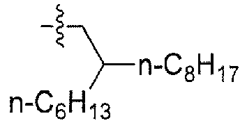

796 S S S n-C11H23 n-C11H23 797 S S S n-C12H25 n-C12H25 798 S S S n-C13H27 n-C13H27 799 S S S n-C14H29 n-C14H29 800 S S S n-C15H31 n-C15H31 801 S S S n-C16H33 n-C16H33 802 S S S n-C17H35 n-C17H35 803 S S S n-C18H37 n-C18H37 804 S S S n-C19H39 n-C19H39 805 S S S n-C20H41 n-C20H41 806 S S S n-C21H43 n-C21H43 807 S S S n-C22H45 n-C22H45 808 S S S n-C23H47 n-C23H47 809 S S S n-C24H49 n-C24H49 810 S S S n-C25H51 n-C25H51 811 S S S n-C26H53 n-C26H53 812 S S S n-C27H55 n-C27H55 813 S S S n-C28H57 n-C28H57 814 S S S n-C29H59 n-C29H59 815 S S S n-C30H61 n-C30H61 816 S S S n-C6F13 n-C6F13 817 S S S n-C8F17 n-C8F17 818 S S S n-C12F25 n-C12F25 819 S S S n-C6H13 H 820 S Se S n-C6H13 n-C6H13 821 Se S Se n-C8H17 n-C8H17 822 S S S n-C6H13 n-C12H25 823 S S S O(n-C4H9) O(n-C4H9) 824 S S S O(n-C5H11) O(n-CsH11) Dashed line indicates a chemical bond. -
Table 89 
Compound No. E1 E2 E3 R1 R2 826 S S S O(n-C6H13) O(n-C6H13) 829 S S S O(n-C7H15) O(n-C7H15) 830 S S S O(n-C8H17) O(n-C8H17) 831 S S S O(n-C9H19) O(n-C9H19) 832 S S S O(n-C10H21) O(n-C10H21) 834 S S S O(n-C11H23) O(n-C11H23) 835 S S S O(n-C12H25) O(n-C12H25) 836 S S S O(n-C13H27) O(n-C13H27) 837 S S S O(n-C14H29) O(n-C14H29) 838 S S S O(n-C15H31) O(n-C15H31) 839 S S S O(n-C16H33) O(n-C16H33) 840 S S S O(n-C17H35) O(n-C17H35) 841 S S S O(n-C18H37) O(n-C18H37) 842 S S S O(n-C19H39) O(n-C19H39) 843 S S S O(n-C20H41) O(n-C20H41) 844 S S S O(n-C21H43) O(n-C21H43) 845 S S S O(n-C22H45) O(n-C22H45) 846 S S S O(n-C23H47) O(n-C23H47) 847 S S S O(n-C24H49) O(n-C24H49) 848 S S S O(n-C25H51) O(n-C25H51) 849 S S S O(n-C26H53) O(n-C26H53) 850 S S S O(n-C27H55) O(n-C27H55) 851 S S S O(n-C28H57) O(n-C28H57) 852 S S S O(n-C29H59) O(n-C29Hs9) 853 S S S O(n-C30H61) O(n-C30H61) 854 S S S O(n-C6F13) O(n-C6F13) 855 S S S O(n-C8F17) O(n-C8F17) 856 S S S O(n-C12F25) O(n-C12F25) 857 S S S O(n-C16F33) O(n-C16F33) 858 S Se S O(n-C6H13) O(n-C6H13) 859 Se S Se O(n-C8H17) O(n-C8H17) Dashed line indicates a chemical bond. -
Table 90 
Compound No. E1 E2 E3 R1 R2 860 S S S O(n-C8H17) O(n-C12H25) 861 S S S 

862 S S S 
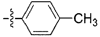
863 S S S 

864 S S S 

865 S S S 

867 S S S 
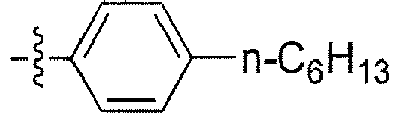
869 S S S 

870 S S S 

872 S S S 

873 S S S 

874 S S S 

Dashed line indicates a chemical bond. -
Table 91 
Compound No. E1 E2 E3 R1 R2 876 S S S 

877 S S S 

878 S S S 

879 S S S 

880 S S S 

882 S S S 

883 S S S 

885 S S S 

886 S S S 
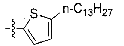
887 S S S 

888 S S S 

889 S S S 

890 S Se S 

Dashed line indicates a chemical bond. -
Table 92 
Compound No. E1 E2 E3 R1 R2 891 S S S 

897 S S S 

900 S S S 

901 S S S 

902 S S S 

903 S S S 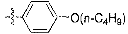

905 S S S 

Dashed line indicates a chemical bond. -
Table 93 
Compound No. E1 E2 E3 R1 R2 907 S S S 

908 S S S 

910 S S S 

911 S S S 

912 S S S 

914 S S S 

915 S S S 

916 S S S 

918 S S S 

919 S S S 

Dashed line indicates a chemical bond. -
Table 94 
Compound No. E1 E2 E3 R1 R2 921 S S S 

922 S S S 

923 S Se S 

924 Se S Se 

925 S S S 

927 S Se S 

928 S S S 

Dashed line indicates a chemical bond. -
Table 95 
Compound No. E1 E2 E3 R1 R2 936 S S S 

937 S S S 

938 S S S 

939 S S S 

940 S S S 

941 S S S 

942 S S S 

943 S S S 
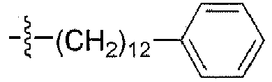
944 S S S 

945 S S S 

946 S S S 

947 S S S 

948 S S S 

950 Se S Se 

951 S S S 

Dashed line indicates a chemical bond. -
Table 96-1 
Compound No. E1 E2 E3 R1 R2 952 S S S 

953 S Se S 

954 S S S 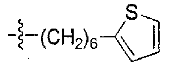

955 S S S 

956 S S S 

957 S S S 

958 S S S 

959 S S S 

960 S S S 

Dashed line indicates a chemical bond. Table 96-2 
Compound No. E1 E2 E3 R1 R2 961 S S S 

962 S S S 

963 Se Se Se 

964 S S S -Si(CH3)3 -Si(CH3)3 965 S S S -Si(C2H5)3 -Si(C2H5)3 966 S S S -Si(i-C3H7)3 -Si(i-C3H7)3 967 S S S -Si(CH3)2(t-C4H9) -Si(CH3)2(t-C4H9) 968 S S S -Si(CH3)2(n-C6H13) -Si(CH3)2(n-C6H13) 969 S S S -Si(CH3)2(n-C12H25) -Si(CH3)2(n-C12H25) Dashed line indicates a chemical bond. -
Table 97 
Compound No. E1 E2 E3 R1 R2 970 S S S n-C4H9 n-C4H9 971 S S S n-C5H11 n-C5H11 972 S S S 

973 S S S n-C6H13 n-C6H13 974 S S S 

975 S S S 

976 S S S n-C8H17 n-C8H17 977 S S S 

978 S S S n-C12H25 n-C12H25 979 S S S n-C13H27 n-C13H27 980 S S S n-C16H33 n-C16H33 981 S S S n-C18H37 n-C18H37 982 S S S n-C20H41 n-C20H41 983 S S S n-C25H51 n-C25H51 984 S S S n-C30H61 n-C30H61 985 S S S n-C6F13 n-C6F13 986 S Se S n-C6H13 n-C6H13 987 Se S Se n-C8H17 n-C8H17 988 S S S n-C6H13 n-C12H25 990 S S S O(n-C6H13) O(n-C6H13) 993 S S S O(n-C8H17) O(n-C8H17) 995 S S S O(n-C12H25) O(n-C12H25) Dashed line indicates a chemical bond. -
Table 98 
Compound No. E1 E2 E3 R1 R2 996 S S S O(n-C8F17) O(n-C8F17) 997 S Se S O(n-C6H13) O(n-C6H13) 998 S S S O(n-C8H17) O(n-C12H25) 999 S S S 

1001 S S S 

1003 S S S 

1004 S S S 

1006 S S S 

1007 S S S 

1009 S S S 

1010 S S S 

1011 S S S 

Dashed line indicates a chemical bond. -
Table 99 
Compound No. E1 E2 E3 R1 R2 1012 S S S 

1013 S S S 

1015 S S S 

1016 S S S 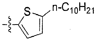

1018 S S S 

1019 S S S 

1020 S S S 

1021 S S S 

1022 S S S 

1026 S S S 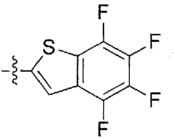

Dashed line indicates a chemical bond. -
Table 100 
Compound No. E1 E2 E3 R1 R2 1029 S S S 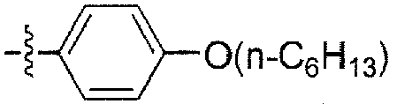

1031 S S S 

1033 S S S 

1034 S S S 

1036 S S S 

1037 S S S 

1039 S S S 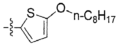

1040 S S S 

Dashed line indicates a chemical bond. -
Table 101 
Compound No. E1 E2 E3 R1 R2 1042 S S S 

1043 S S S 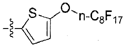
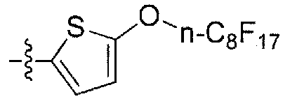
1044 S Se S 

1045 S S S 

1049 S S S 

1050 S S S 

1051 S S S 

1052 S S S 

1053 S S S 

1054 S S S 

1055 S S S 

Dashed line indicates a chemical bond. -
Table 102 
Compound No. E1 E2 E3 R1 R2 1056 Se S Se 

1057 S S S 

1058 S S S 

1059 S S S 

1060 S S S 

1061 S S S 

1062 S S S 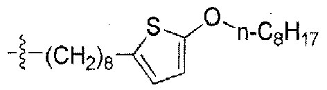

1063 S S S 

1064 S S S 

1065 S S S 

1066 S S S -Si(CH3)3 -Si(CH3)3 Dashed line indicates a chemical bond. -
Table 103 
Compound No. E1 E2 E3 R1 R2 1067 S S S n-C6H13 n-C6H13 1068 S S S n-C12H25 n-C12H25 1069 S S S n-C13H27 n-C13H27 1070 S S S n-C6F13 n-C6F13 1071 S S S O(n-C6H13) O(n-C6H13) 1072 S S S 

1073 S S S 

1074 S S S 

1075 S S S 

1079 S S S 

1083 S S S 
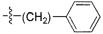
1084 S S S 

Dashed line indicates a chemical bond. -
Table 104 
Compound No. E1 E2 E3 R1 R2 1085 Se S Se 

1086 S S S 

1087 S S S 

1088 S S S 

1089 S S S 

1090 S S S -Si(CH3)3 -Si(CH3)3 Dashed line indicates a chemical bond. -
Table 105 
Compound No. E1 E2 E3 R1 R2 1091 S S S n-C6H13 n-C6H13 1092 S S S O(n-C6H13) O(n-C6H13) 1093 S S S 

1094 S S S 

Dashed line indicates a chemical bond. -
Table 106 
Compound No. E1 E2 E3 R1 R2 1100 S S S 

1101 S S S 

1102 S S S 
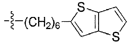
1103 S S S 

1104 S S S -Si(CH3)3 -Si(CH3)3 Dashed line indicates a chemical bond. -
Table 107 
Compound No. E1 E2 E3 R1 R2 1105 S S S n-C6H13 n-C6H13 1106 S S S O(n-C6H13) O(n-C6H13) 1107 S S S 

1108 S S S 

Dashed line indicates a chemical bond. -
Table 108 
Compound No. E1 E2 E3 R1 R2 1115 S S S 

1116 S S S 

1117 S S S 

1118 S S S 

1119 S S S -Si(CH3)3 -Si(CH3)3 Dashed line indicates a chemical bond. -
Table 109 
Compound No. E1 E2 E3 R1 R2 1120 S S S n-C6H13 n-C6H13 1121 S S S 

1124 S S S 

1125 S S S 

1126 S S S -Si(CH3)3 -Si(CH3)3 Dashed line indicates a chemical bond. -
Table 110 
Compound No. E1 E2 E3 R1 R2 1127 S S S n-C6H13 n-C6H13 1128 S S S 

1131 S S S 

1132 S S S 

1133 S S S -Si(CH3)3 -Si(CH3)3 Dashed line indicates a chemical bond. -
Table 111 
Compound No. E1 E2 E3 R1 R2 1134 S S S n-C6H13 n-C6H13 1135 S S S 

1138 S S S 

1139 S S S 

1140 S S S -Si(CH3)3 -Si(CH3)3 Dashed line indicates a chemical bond. - One example of a production process of the compound (5-1) used for the present 1st reaction is described for the case that R1 and R2 are the same kinds (hereinafter, optionally described as R) as follows. That is, the compound (5-1) can be produced by the so-called Glaser Reaction, the Eglinton Coupling or the Hay Coupling (preferably, the Hay Coupling utilizing a copper compound such as copper iodide) by using, for example, a compound represented by the formula (6-1):

The Hay Coupling can be carried out, for example, in the presence of N,N,N',N'-tetramethyethylnediamine (TMEDA) and a copper compound such as copper iodide according to the reaction formula below.
- brominating aniline having a substituent R with N-bromosuccinimide, etc. in the α-position of the amino group,
- converting the amino group of thus obtained compound into an iodine group by the Sandmeyer Reaction, and
- carrying out an ethynylation of the iodine group in thus obtained iodine-containing compound by the Sonogashira Cross-coupling Reaction, etc.
- The specific examples of the compound represented by the formula (6-1) are illustrated in the following tables.
Table 112 
Compound No. X1 R1 1711 Br n-C4H9 1712 Br s-C4H9 1713 Br n-C5H11 1714 Br 
1715 Br n-C6H13 1716 Br 
1717 Br 
1718 Br n-C7H15 1719 Br n-C8H17 1720 Br n-C9H19 1721 Br n-C10H21 1722 Br 
1723 Br n-C11H23 1724 Br n-C12H25 1725 Br n-C13H27 Dashed line indicates a chemical bond. -
Table 113 
Compound No. X1 R1 1726 Br n-C14H29 1727 Br n-C15H31 1728 Br n-C16H33 1729 Br n-C17H35 1730 Br n-C18H37 1731 Br n-C19H39 1732 Br n-C20H41 1733 Br n-C21H43 1734 Br n-C22H45 1735 Br n-C23H47 1736 Br n-C24H49 1737 Br n-C25H51 1738 Br n-C26H53 1739 Br n-C27H55 1740 Br n-C28H57 1741 Br n-C29H59 1742 Br n-C30H61 1743 Br n-C6F13 1744 Br n-C8F17 1745 Br n-C12F25 1746 Br H 1747 I n-C6H13 1748 I n-C8H17 1749 C1 n-C8H17 1750 Br O(n-C4H9) 1751 Br O(n-C5H11) 1753 Br O(n-C6H13) 1756 Br O(n-C7H15) 1757 Br O(n-C8H17) 1758 Br O(n-C9H19) 1759 Br O(n-C10H21) Dashed line indicates a chemical bond. -
Table 114 
Compound No. X1 R1 1761 Br O(n-C11H23) 1762 Br O(n-C12H25) 1763 Br O(n-C13H27) 1764 Br O(n-C14H29) 1765 Br O(n-C15H31) 1766 Br O(n-C16H33) 1767 Br O(n-C17H35) 1768 Br O(n-C18H37) 1769 Br O(n-C19H39) 1770 Br O(n-C20H41) 1771 Br O(n-C21H43) 1772 Br O(n-C22H45) 1773 Br O(n-C23H47) 1774 Br O(n-C24H49) 1775 Br O(n-C25H51) 1776 Br O(n-C26H53) 1777 Br O(n-C27H55) 1778 Br O(n-C28H57) 1779 Br O(n-C29H59) 1780 Br O(n-C30H61) 1781 Br O(n-C6F13) 1782 Br O(n-C8F17) 1783 Br O(n-C12F25) 1784 Br O(n-C16F33) 1785 I O(n-C6H13) 1786 I O(n-C8H17) 1787 C1 O(n-C8H17) 1788 Br 
1789 Br 
Dashed line indicates a chemical bond. -
Table 115 
Compound No. X1 R1 1790 Br 
1791 Br 
1792 Br 
1794 Br 
1796 Br 
1797 Br 
1799 Br 
1800 Br 
1801 Br 
1803 Br 
1804 Br 
1805 Br 
Dashed line indicates a chemical bond -
Table 116 
Compound No. X1 R1 1806 Br 
1807 Br 
1809 Br 
1810 Br 
1812 Br 
1813 Br 
1814 Br 
1815 Br 
1816 Br 
1817 Br 
1818 Br 
Dashed line indicates a chemical bond. -
Table 117 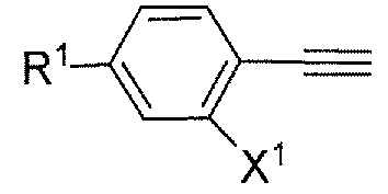
Compound No. X1 R1 1824 Br 
1827 Br 
1828 Br 
1829 Br 
1830 Br 
1832 Br 
1834 Br 
Dashed line indicates a chemical bond. -
Table 118 
Compound No. X1 R1 1835 Br 
1837 Br 
1838 Br 
1839 Br 
1841 Br 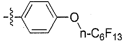
1842 Br 
1843 Br 
1845 Br 
1846 Br 
1848 Br 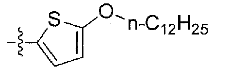
1849 Br 
-
Table 119 
Compound No. X1 R1 1850 Br 
1851 Br 
1852 Br 
1853 Br 
1854 Br 
Dashed line indicates a chemical bond. -
Table 120 
Compound No. X1 R1 1862 Br 
1863 Br 
1864 Br 
1865 Br 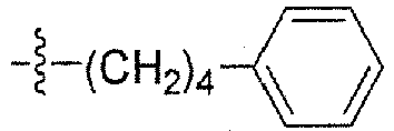
1866 Br 
1867 Br 
1868 Br 
1869 Br 
1870 Br 
1871 Br 
1872 Br 
1873 Br 
1874 Br 
1875 Br 
Dashed line indicates a chemical bond. -
Table 121-1 
Compound No. X1 R1 1876 Br 
1877 Br 
1878 Br 
1879 Br 
1880 Br 
1881 Br 
1882 Br 
1883 Br 
1884 Br 
Dashed line indicates a chemical bond. Table 121-2 
Compound No. X1 R1 1885 Br 
1886 Br 
1887 Br 
1888 Br 
1889 Br 
1890 Br 
1891 Br 
1892 Br 
1893 Br 
1894 Br 
Dashed line indicates a chemical bond. -
Table 122-1 
Compound No. X1 R1 1895 Br 
1896 Br 
1897 Br 
1898 Br 
1899 Br 
1900 Br 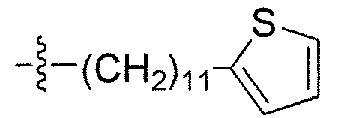
1901 Br 
1902 Br 
1903 Br 
1904 Br 
Dashed line indicates a chemical bond. Table 122-2 
Compound No. X1 R1 1905 Br 
1906 Br 
1907 Br 
1908 Br 
1909 Br 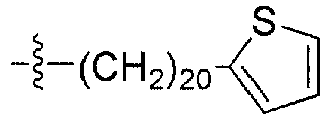
1910 Br 
1911 Br 
1912 Br 
1913 Br 
Dashed line indicates a chemical bond. -
Table 123 
Compound No. X1 R1 1914 Br 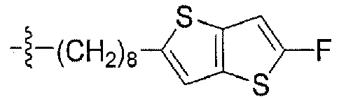
1915 Br 
1916 Br 
1917 Br 
1918 Br -Si(CH3)3 1919 Br -Si(C2H5)3 1920 Br -Si(i-C3H7)3 1921 Br -Si(CH3)2(t-C4H9) 1922 Br -Si(CH3)2(n-C6H13) 1923 Br -Si(CH3)2(n-C12H25) Dashed line indicates a chemical bond. -
Table 124 
Compound No. X1 R1 1924 Br n-C4H9 1925 Br s-C4H9 1926 Br n-C5H11 1927 Br 
1928 Br n-C6H13 1929 Br 
1930 Br 
1931 Br n-C7H15 1932 Br n-C8H17 1933 Br n-C9H19 1934 Br n-C10H21 1924 Br n-C4H9 1926 Br n-C5H11 1928 Br n-C6H13 1931 Br n-C7H15 1932 Br n-C8H17 1933 Br n-C9H19 1934 Br n-C10H21 Dashed line indicates a chemical bond. -
Table 125 
Compound No. X1 R1 1935 Br 
1936 Br n-C11H23 1937 Br n-C12H25 1938 Br n-C13H27 1939 Br n-C14H29 1940 Br n-C15H31 1941 Br n-C16H33 1942 Br n-C17H35 1943 Br n-C18H37 1944 Br n-C19H39 1945 Br n-C20H41 1946 Br n-C21H43 1947 Br n-C22H45 1948 Br n-C23H47 1949 Br n-C24H49 1950 Br n-C25H51 1951 Br n-C26H53 1952 Br n-C27H55 1953 Br n-C28H57 1954 Br n-C29H59 1955 Br n-C30H61 1956 Br n-C6F13 1957 Br n-C8F17 1958 Br n-C12F25 1959 Br n-C16F33 1960 I n-C6H13 1961 Cl n-C8H17 1962 Br n-C6H13 1963 Br O(n-C4H9) 1964 Br O(n-C5H11) Dashed line indicates a chemical bond. -
Table 126 
Compound No. X1 R1 1966 Br O(n-C6H13) 1969 Br O(n-C7H15) 1970 Br O(n-C8H17) 1971 Br O(n-C9H19) 1972 Br O(n-C10H21) 1974 Br O(n-C11H23) 1975 Br O(n-C12H25) 1976 Br O(n-C13H27) 1977 Br O(n-C14H29) 1978 Br O(n-C15H31) 1979 Br O(n-C16H33) 1980 Br O(n-C17H35) 1981 Br O(n-C18H37) 1982 Br O(n-C19H39) 1983 Br O(n-C20H41) 1984 Br O(n-C21H43) 1985 Br O(n-C22H45) 1986 Br O(n-C23H47) 1987 Br O(n-C24H49) 1988 Br O(n-C25H51) 1989 Br O(n-C26H53) 1990 Br O(n-C27H55) 1991 Br O(n-C28H57) 1992 Br O(n-C29H59) 1993 Br O(n-C30H61) 1994 Br O(n-C6F13) 1995 Br O(n-C8F17) 1996 Br O(n-C12F25) 1997 Br O(n-C16F33) 1998 I O(n-C6H13) 1999 Cl O(n-C8H17) Dashed line indicates a chemical bond. -
Table 127 
Compound No. X1 R1 2000 Br O(n-C8H17) 2001 Br 
2002 Br 
2003 Br 
2004 Br 
2005 Br 
2007 Br 
2009 Br 
2010 Br 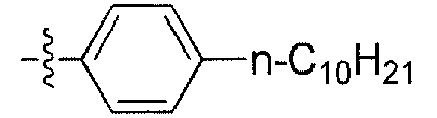
2012 Br 
2013 Br 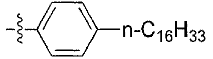
2014 Br 
Dashed line indicates a chemical bond. -
Table 128-1 
Compound No. X1 R1 2016 Br 
2017 Br 
2018 Br 
2019 Br 
2020 Br 
2022 Br 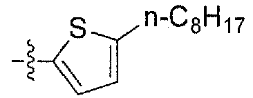
2023 Br 
Dashed line indicates a chemical bond. Table 128-2 
Compound No. X1 R1 2025 Br 
2026 Br 
2027 Br 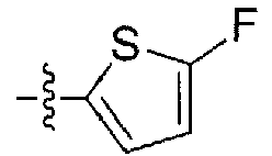
2028 Br 
2029 Br 
2030 Br 
Dashed line indicates a chemical bond. -
Table 129 
Compound No. X1 R1 2031 Br 
2037 Br 
2040 Br 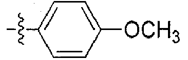
2041 Br 
2042 Br 
2043 Br 
2045 Br 
Dashed line indicates a chemical bond. -
Table 130 
Compound No. X1 R1 2047 Br 
2048 Br 
2050 Br 
2051 Br 
2052 Br 
2054 Br 
2055 Br 
2056 Br 
2058 Br 
2059 Br 
Dashed line indicates a chemical bond. -
Table 131 
Compound No. X1 R1 2061 Br 
2062 Br 
2063 Br 
2064 Br 
2065 Br 
2066 Br 
2067 Br 
Dashed line indicates a chemical bond. -
Table 132-1 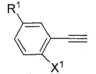
Compound No. X1 R1 2075 Br 
2076 Br 
2077 Br 
2078 Br 
2079 Br 
2080 Br 
2081 Br 
2082 Br 
2083 Br 
Dashed line indicates a chemical bond. Table 132-2 
Compound No. X1 R1 2084 Br 
2085 Br 
2086 Br 
2087 Br 
2088 Br 
2089 Br 
2090 Br 
2091 Br 
Dashed line indicates a chemical bond. -
Table 133-1 
Compound No. X1 R1 2092 Br 
2093 Br 
2094 Br 
2095 Br 
2096 Br 
2097 Br 
2098 Br 
2099 Br 
2100 Br 
Dashed line indicates a chemical bond. Table 133-2 
Compound No. X1 R1 2101 Br 
2102 Br 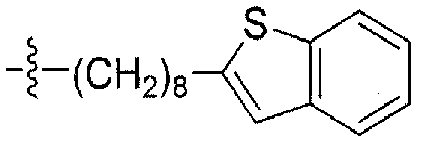
2103 Br 
2104 Br -Si(CH3)3 2105 Br -Si(C2H5)3 2106 Br -Si(i-C3H7)3 2107 Br -Si(CH3)2(t-C4H9) 2108 Br -Si(CH3)2(n-C6H13) 2109 Br -Si(CH3)2(n-C12H25) Dashed line indicates a chemical bond. -
Table 134 
Compound No. X1 R1 2110 Br n-C4H9 2111 Br n-C5H11 2112 Br 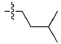
2113 Br n-C6H13 2114 Br 
2115 Br 
2116 Br n-C8H17 2117 Br 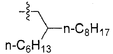
2118 Br n-C12H25 2119 Br n-C13H27 2120 Br n-C16H33 2121 Br n-C18H37 2122 Br n-C20H41 2123 Br n-C25H51 2124 Br n-C30H61 2125 Br n-C6F13 2126 I n-C6H13 2127 C1 n-C8H17 2128 Br O(n-C4H9) 2130 Br O(n-C6H13) 2133 Br O(n-C8H17) 2135 Br O(n-C12H25) Dashed line indicates a chemical bond. -
Table 135 
Compound No. X1 R1 2136 Br O(n-C8F17) 2137 I O(n-C6H13) 2138 Br O(n-C8H17) 2139 Br 
2141 Br 
2143 Br 
2144 Br 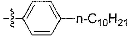
2146 Br 
2147 Br 
2149 Br 
2150 Br 
2151 Br 
Dashed line indicates a chemical bond. -
Table 136 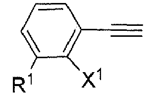
Compound No. X1 R1 2152 Br 
2153 Br 
2155 Br 
2156 Br 
2158 Br 
2159 Br 
2160 Br 
2161 Br 
2162 Br 
2166 Br 
Dashed line indicates a chemical bond. -
Table 137 
Compound No. X1 R1 2169 Br 
2171 Br 
2173 Br 
2174 Br 
2176 Br 
2177 Br 
2179 Br 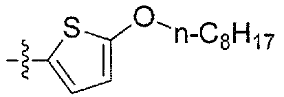
2180 Br 
Dashed line indicates a chemical bond. -
Table 138 
Compound No. X1 R1 2182 Br 
2183 Br 
2184 Br 
2185 Br 
2189 Br 
2190 Br 
2191 Br 
2192 Br 
2193 Br 
2194 Br 
2195 Br 
Dashed line indicates a chemical bond. -
Table 139 
Compound No. X1 R1 2196 Br 
2197 Br 
2198 Br 
2199 Br 
2200 Br 
2201 Br 
2202 Br 
2203 Br 
2204 Br 
2205 Br 
2206 Br -Si(CH3)3 Dashed line indicates a chemical bond. -
Table 140 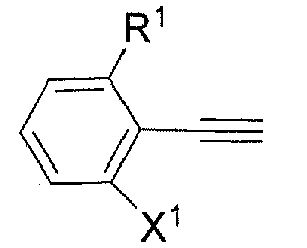
Compound No. X1 R1 2207 Br n-C6H13 2208 Br n-C12H25 2209 Br n-C13H27 2210 Br n-C6F13 2211 Br O(n-C6H13) 2212 Br 
2213 Br 
2214 Br 
2215 Br 
2219 Br 
2223 Br 
2224 Br 
Dashed line indicates a chemical bond. -
Table 141 
Compound No. X1 R1 2225 Br 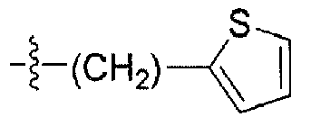
2226 Br 
2227 Br 
2228 Br 
2229 Br 
2230 Br -Si(CH3)3 Dashed line indicates a chemical bond. - A process for producing the substituted benzochalcogenoacene compound (1) in the case that R1 and R2 are the same or different kinds, is exemplified by a process according to the description of the non-patent literature 1 (Advanced Materials, 19, 3008-3011 (2007)). That is, the process comprises the sequential steps of:
- brominating the benzo[b]thiophene having R1 or R2 with bromine,
- working lithiumisopropylamide (LDA) on the brominated product thus obtained, then
- carrying out a coupling reaction using copper chloride, and
- working butyl lithium (BuLi) and bis(phenylsulfonyl)sulfide ((C6H5SO2)2S) on the coupling product thus obtained to produce the compound (1), as shown in the following reaction sequence scheme.
- An organic semiconductor device of the present invention will be explained as follows.
A thin film of the present invention comprises the substituted benzochalcogenoacene compound (1). The thin film shows high carrier mobility. Therefore, the thin film is suitable for a material for an organic semiconductor device having the thin film as an active organic semiconductor layer.
In addition, the organic semiconductor device of the present invention comprises the thin film of the present invention. Examples of the organic semiconductor device of the present invention include an organic transistor, an electroluminescence device and a solar cell. The organic transistor of the present invention can be used, for example, in an electronic paper, a flexible display, an IC tag and a sensor. - The formation process of the thin film of the present invention is exemplified by the applying and film-forming process. The applying and film-forming process means the film-forming process which comprises the steps of dissolving the substituted benzochalcogenoacene compound (1) in a solvent and applying the obtained solution composition on a substrate or an insulating layer.
Examples of the coating process include a casting process, a dip coat process, a die coater process, a roll coater process, a bar coater process, an ink jet process, a screen printing process, an offset printing process and a microcontact printing process. These processes can be used alone or in combination of two or more of these processes. - A relevant solvent which is used for the preparation of the above solution composition can be selected properly depending on the kind of the substituted benzochalcogenoacene compound to be applied. Preferable examples of the solvent include an aromatic hydrocarbon solvent such as benzene, toluene, xylene, chlorobenzene and o-dichlorobenzene, a halogenated hydrocarbon solvent such as dichloromethane, chloroform, 1,2-dichloroethane, 1,1',2,2'-tetrachloroethane, tetrachlorocarbon, an ether solvent such as tetrahydrofuran and dioxane, and an aliphatic hydrocarbon solvent such as pentane, hexane, heptane, octane and cyclohexane. Among them, toluene, xylene, o-dichlorobenzene, dichloromethane, chloroform, tetrahydrofuran and hexane are preferable. These solvents can be used also by mixing two or more of them. The concentration of the substituted benzochalcogenoacene compound (1) in the solution composition is 0.01-50 wt%, preferably, 0.01-10 wt%, more preferably, 0.1-5 wt%. Additionally, within the range where carrier mobility is not damaged remarkably, additives such as an antioxidant or a stabilizer can be contained in the solution composition. The solution composition can be obtained by dissolving the substituted benzochalcogenoacene compound (1) in the solvent at temperatures of, for example, 10-200°C, preferably, 20-150°C.
- After the solution composition thus obtained is applied to a substrate or an insulating layer to result in the formation of a coated film, a thin film can be formed on the substrate or the insulating layer by eliminating the solvent contained in the coated film. In order to eliminate the solvent, a naturally drying treatment, a heating treatment, a reduced pressure treatment, a draught drying treatment and a combination thereof can be adopted. Among them, the naturally drying treatment or the heating treatment are preferable from the point of easy operation. The operation condition for the treatment is described as still-standing under the atmosphere or heating of the substrate on a hot plate (for example, at 40-250°C, preferably, 50-250°C).
- The thin film of the present invention can be formed by the applying and film-forming process by using also a dispersion of the substituted benzochalcogenoacene compound (1) in the solvent, and in this case, the process can be easily carried out by reading the solution composition as the dispersion composition.
Thus, the thin film of the present invention can be formed by a simple method such as the applying and film-forming process as described above. - Another different example of the thin film forming process of the present invention is a thin film forming process under vacuum such as a vacuum deposition process, a sputtering process, a CVD process and a molecular beam epitaxial process.
- In the vacuum deposition process, the substituted benzochalcogenoacene compound is heated in a crucible or a metal boat under vacuum, and the evaporated organic semiconductor material is deposited on the substrate or the insulating material. A degree of vacuum when deposition occurs is, generally, 1x10⁻¹ Pa or lower, preferably, 1x10⁻³ Pa or lower. A substrate temperature when deposition occurs is, generally, 0°C -300°C, preferably, 20°C -200°C. A deposition speed is, for example, 0.001nm/sec - 10nm/sec, preferably, 0.01nm/sec - 1nm/sec.
- A thickness of the thin film comprising the substituted benzochalcogenoacene compound (1) obtained by the above applying and film-forming process or the above vacuum process is controllable, for example, depending on a device structure of the organic transistor, and the film thickness is preferably 1nm-10µm, more preferably, 5nm-1µm.
- An example of the organic transistor of the present invention is the organic field effect transistor (OFET).
The structure of the organic field effect transistor is, for example, generally provided with a source electrode and a drain electrode close to the organic semiconductor active layer consisting of the thin film of the present invention, and further provided with a gate electrode across an insulator layer (a dielectric layer) close to the organic semiconductor active layer.
Examples of the device structure include the followings: - (1) a structure of a substrate/a gate electrode/an insulating layer/a source electrode-a drain electrode/an organic semiconductor active layer (refer to
Fig. 1 ), - (2) a structure of a substrate/a gate electrode/an insulating layer/an organic semiconductor active layer/a source electrode-a drain electrode (refer to
Fig. 2 ), - (3) a structure of a substrate/an organic semiconductor active layer/a source electrode-a drain electrode/an insulating layer/a gate electrode,
- (4) a structure of a substrate/a source electrode (or a drain electrode) /an organic semiconductor active layer + an insulating layer + a gate electrode/a drain electrode (or a source electrode).
- The other components of the organic transistor will be explained by illustrating specific examples.
In manufacturing the organic transistor in the present invention, materials constituting the source electrode, the drain electrode and the gate electrode are not limited specifically as far as the materials are electrically conducting materials such as platinum, gold, silver, nickel, chromium, copper, iron, tin, lead antimony, tantalum, indium, palladium, tellurium, rhenium, iridium, aluminum, ruthenium, germanium, molybdenum, molybdenum oxide, tungsten, antimony tin oxide, indium tin oxide (ITO), zinc doped with fluorine, zinc, carbon, graphite, a glassy carbon, a silver paste and carbon paste, lithium, beryllium, sodium, magnesium, potassium, calcium, scandium, titanium, manganese, zirconium, gallium, niobium, sodium, a sodium-potassium alloy, magnesium, lithium, aluminum, a magnesium/ copper mixture, a magnesium/silver mixture, a magnesium/aluminum mixture, a magnesium/indium mixture, an aluminum/aluminum oxide mixture and a lithium/aluminum mixture. Especially, platinum, gold, silver, molybdenum oxide, indium, ITO and carbon are preferable. In addition, known conductive polymers whose conductivity is improved by doping, etc. are also suitably used. Examples of such conductive polymers include a conductive polyaniline, a conductive polypyrrole, a conductive polythiophene and a complex between polyethylenedioxythiophene and polystyrene sulfonic acid. Above all, the conductive materials which have a low electric resistance at the contact face with the semiconductor layer are preferable. These conductive materials may be used alone or in a mixture of two or more kinds. A film thickness of the electrode varies depending on the material, and the thickness is, preferably, 0.1nm-10µm, further preferably, 0.5nm-5µm, and more preferably, 1nm-3µm. In addition, when the gate electrode doubles with the substrate, the film thickness may be larger than the above values. - The source electrode and the drain electrode used in the organic transistor of the present invention may undergo a surface treatment. The surface treatment of the electrode surface contacting with the thin film (the organic semiconductor active layer) of the present invention is preferable, since the surface treatment tends to improve the transistor performances of the organic transistor comprising the thin film. An example of the surface treatment is a modification process of the electrode surfaces mentioned above by dipping the electrodes in an alcohol solution of, for example, a saturated hydrocarbon compound having a thiol group such as 1-octylthiol, 1-perfluorooctylthiol, 1-octadecylthiol and 1-perfluorooctadecylthiol, an aromatic compound having a thiol group such as benzenethiol and perfluorobenzenethiol, and a heteroaromatic compound having a thiol group such as thienylthiol and perfluoro-thienylthiol.
- The electrode can be manufactured by various methods using above raw materials. Specifically, a vacuum deposition method, a sputtering method, a coating method, a thermal transfer method, a printing method and a sol-gel method are exemplified. At or after the film-forming, it is preferable to carry out patterning, optionally. The patterning can be carried out by using various methods. Specifically, a photolithography method which combines a patterning and an etching of the photoresist is exemplified. In addition, soft-lithography methods such as an inkjet printing, a screen printing, an offset printing and an anastatic printing are exemplified. These methods can be used for the patterning, alone or in combination of two or more of them.
- Various insulating films can be used as the insulating layer. Inorganic oxides, inorganic nitrides and organic compounds can be exemplified as materials for the insulating films.
Examples of inorganic oxides include silicon oxide, aluminum oxide, tantalum oxide, titanium oxide, tin oxide, vanadium oxide, strontium barium titanate, barium titanate zirconate, lead titanate zirconate, lanthanum lead titanate, strontium titanate, barium titanate, magnesium barium fluoride, bismuth titanate, bismuth strontium titanate, bismuth strontium tantalite, bismuth niobate tantalite and yttrium trioxide. Silicon oxide, aluminum oxide, tantalum oxide and titanium oxide are preferable. Examples of the organic compounds include polyimide, polyamide, polyester, polyacrylate, a photo-curable resin obtained by photo-radical polymerization or photo-cationic polymerization, a copolymer comprising an acrylonitrile component, polyvinylphenol, polyvinylalcohol, a novolak resin and cyanoethylpullulan. Polyimide, polyvinylphenol and polyvinylalcohol are preferable. These materials for the insulating layer can be used alone or in combination of two or more of them. A thickness of the insulating layer varies depending on the material, and the thickness is, preferably, 0.1nm-100µm, further preferably, 0.5nm-50µm, and more preferably, 5nm-10µm. - The insulating layer can be formed by various methods. Specifically, a spin coating, a spray coating, a dip coating, a cast, a bar coating, a blade coating, a screen printing, an offset printing, an inkjet and dry process methods such as a vacuum deposition, a molecular beam epitaxial growth method, an ion cluster beam method, an ion plating method, a sputtering method, an atmospheric plasma method and a CVD method are exemplified. In addition, a sol-gel method and a method in which an oxide film is formed on a metal substrate such as an alumite on aluminum or a thermal oxide film of silicon are exemplified.
- Examples of the materials of the substrate include glass, paper, quartz, ceramic and a resin sheet. Specified examples of materials for the resin sheet include polyethylene terephthalate (PET), polyethylene naphthalate (PEN), polyether sulfone (PES), polyetherimide, polyether ether ketone, polyphenylene sulfide, polyarylate, polyimide, polycarbonate (PC), cellulose triacetate (TAC) and cellulose acetate propionate (CAP). The thickness of the substrate is, preferably, 1µm-10mm, more preferably, 5µm-5mm.
- In the contact parts of the insulating layer and the substrate with the thin film of the present invention (hereinafter, optionally described as the organic semiconductor active layer), a surface treatment may be carried out on the insulating layer and the substrate. By the surface treatment of the insulating layer on which the organic semiconductor active layer is laminated, the transistor performance of the organic transistor can be improved. The surface treatment is exemplified specifically by a hydrophorbic treatment by hexamethyldisilazane, octadecyltrichlorosilane, octyltrichlorosilane and phenetyltrichlorosilane, an acid treatment by hydrochloric acid, sulfuric acid and an aqueous hydrogen peroxide solution, an alkaline treatment by sodium hydroxide, potassium hydroxide, calcium hydroxide and an aqueous ammonia, an ozone treatment, a hydrogen fluoride treatment, a plasma treatment such as oxygen and argon, a film-forming treatment of Langmuir-Brodgett film, a thin-film forming treatment of other insulator and semiconductor films, a mechanical treatment, an electric treatment such as corona discharge and a rubbing treatment using fibers.
- Processes for the surface treatment are exemplified by a vacuum deposition process, a sputtering process, a coating process, a printing process and a sol-gel process.
- A protective film consisting of resins or inorganic compounds may be laminated on the organic semiconductor active layer. The formation of the protective film inhibits influences from the outer circumstances to result in stabilization of the transistor drive.
- The thin film of the present application exhibits a high carrier-mobility, since it comprises the substituted benzochalcogenoacene compound (1). Therefore, the thin film of the present application is useful as the organic semiconductor active layer in the organic transistor, and the organic transistor having the organic semiconductor active layer comprising the thin film of the present invention exhibits excellent transistor performances and is useful for the organic semiconductor device.
- The present invention is further explained in detail by the following examples.
-

- To a mixture solution of 4-hexylaniline (manufactured by Wako Pure Chemical Industries, Ltd.) (50.53g, 285mmol), ammonium acetate (AcONH4: 2.20g, 28.5mmol) and acetonitrile (MeCN: 855mmol) in a flask dipped in a water bath, N-bromosuccinimide (NBS: 53.26g, 299.3mmol) was added, and after the water bath was taken off, the reaction mixture was stirred for 3 hours. Then, the reaction solution was condensed by an evaporator, followed by addition of ethyl acetate and washing with water and brine. The organic phase was extracted and dried with sodium sulfate, followed by condensation by the evaporator to give an oil product. The oil product was purified by a silica gel column to give 2-bromo-4-hexylaniline (35.63g, 139.1mmol, yield 48.8%).
1H-NMR(CDCl3, δ ppm): 7.22 (d, J=1.9Hz, 1H), 6.91 (dd, J=8.1, 1.9Hz, 1H), 6.68 (d, J=8.1Hz, 1H), 3.93(s, 2H), 2.46(t, J=7.7Hz, 2H), 1.62-1.47 (m, 2H), 1.36-1.24 (m,6H), 0.88(t, J=6.8Hz, 3H) -

- To a mixture solution of 2-bromo-4-hexylaniline (25.62g, 100.0mmol) obtained in the Preparation example 1 and water 450mL, a concentrated sulfuric acid 50g was added in drops, and the mixture was cooled to 5°C. An aqueous solution (water 20mL) of sodium sulfite (NaSO3: 8.97g, 130.0mmol) was added in drops into the mixture and stirring was continued at 10°C for 2 hours, and subsequently, the reaction mixture was added to an aqueous solution (water 300ml) of potassium iodide (KI:132.8g, 0.80mol) at 5°C. Then, after stirring at room temperature (about 24°C) for 6 hours, the reaction mixture was refluxed for 20 minutes by heating, and then cooled to the room temperature. Subsequently, the reaction mixture was poured into an aqueous solution (water 450mL) of sodium sulfite (22.5g, 216.2mmol). Ethyl acetate was added to the reaction mixture, then, the organic phase was extracted, dried with magnesium sulfate and condensed by the evaporator to result in the formation of a brown oil (28.15 g) which contains 2-bromo-4-hexyl-1-iodobenzene as a main component (76.7mmol, yield 76.7%). 1H-NMR (CDCl3, δppm): 7.72 (d, J=8.1Hz, 1H), 7.45 (d, J=2.0Hz, 1H), 6.81 (dd, J=8.1, 2.0Hz, 1H), 2.52 (t, J=7.5Hz, 2H), 1.59-1.54 (m, 2H), 1.36-1.29 (m, 6H), 0.88(t, J=6.7Hz, 3H)
MS-EI 366, 368 (M+), 299, 297 (M-C5H11), 217(M-C5H11Br) -

- To a mixture of the oil 14.68g (40.0mmol) obtained in the Preparation example 2, tetrakis(triphenylphosphine)palladium (Pd(PPh3)4: 0.28g, 0.40mmol), copper iodide (CuI: 0.15g, 0.80mmol) and diisopropylamine ((i-Pr)2NH:53.6mL), a diisopropylamine (26.4mL) solution of trimethylsilylacetylene (Me3Si-C≡CH (TMS-C≡CH): 4.71g, 48.0mmol) was added in drops at room temperature, and stirring was continued for 2 hours. After cutting off a precipitated salt by a silica gel short column and condensing a filtrate, an oil was obtained in which 2-bromo-4-hexyl-1-(trimethylsilyl)ethynylbenzene is a main component. The obtained oil was diluted with tetrahydrofuran (THF: 80mL) and methanol (MeOH: 80mL), and subsequently, at room temperature, potassium carbonate (K2CO3:0.55g, 4.0mmol) was added thereto, followed by stirring for 3 hours. After the solvent was distilled off, a 1% aqueous solution of sodium ammonium and ether were added, and the organic phase was dried with magnesium sulfate, followed by condensation to result in a formation of light brown oil. Purification by a silica gel column using hexane as a developing solvent gave 2-bromo-1-ethynyl-4-hexylbenzene (hereinafter, optionally described as a compound [1715]) represented by the formula [1715] (7.56g, 28.5mmol, yield 71.2%).
1H-NMR (CDCl3, δppm): 7.42 (d, J=7.8Hz, 1H), 7.41 (d, J=1.8Hz, 1H), 7.07 (dd, J=7.8, 1.8Hz, 1H), 3.32 (s, 1H), 2.57 (t, J=7.7Hz, 2H), 1.67-1.51 (m, 2H), 1.37-1.22 (m, 6H), 0.88 (t, J=6.7Hz, 3H)
MS-EI 266, 264(M+), 195, 193(M-C5H11), 115(M-C5H11Br) -

- To an acetone solution (100mL) of copper iodide (CuI: 0.95g, 5.0mmol) and N,N,N',N'-tetramethylethylenediamine (TMEDA: 1.5mL, 10.0mmol), was added the compound [1715] (26.5g, 100.0mmol) obtained in the Preparation example 3, followed by stirring for 5 hours under air bubbling. Acetone was distilled off under vacuum, a 1N-hydrochloric acid was added to the residue, and then, the residue was extracted with chloroform and dried with magnesium sulfate, followed by condensation. Recrtstallization from toluene gave an orange powder of the compound represented by the formula [1145] 1,4-bis(2-bromo-4-hexylphenyl)-diacetylene (hereinafter, optionally described as the compound [1145]) (11.8g, 22.0mmol, yield 45.0%).
1H-NMR (CDCl3, δppm): 7.46 (d, J=7.8Hz, 2H), 7.42 (d, J=1.6Hz, 2H), 7.08 (dd, J=7.8, 1.6Hz, 2H), 2.58 (t, J=7.6Hz, 4H), 1.66-1.50 (m, 4H), 1.38-1.23 (m, 12H), 0.88 (t, J=6.7Hz, 6H)
MS-EI 528(M+), 457(M-C5H11), 386(M-C10H22) -

- The compound [1145] (10.6g, 20mmol) obtained in the Preparation example 4 was dissolved in THF 200mL, and to this solution, under nitrogen atmosphere at -78°C, a 1.59M pentane solution (62.9mL, 100.0mmol) of t-BuLi was added in drops. After stirring at -78°C for 1 hour, a sulfur powder (3.2g, 100.0mmol) was added by small pieces, and subsequently, the temperature was slowly raised to room temperature and stirring was continued for 2 hours. A 1M sodium hydroxide solution (300mL) and K3Fe (CN)6 (32.9g, 100.0mmol) were added, and after stirring for 1 hour at room temperature, chloroform was added to extract the organic phase. The organic phase was washed with saturated brine, dried with magnesium sulfate and condensed by an evaporator. By recrystallization from hexane, the compound represented by the formula [575] was obtained as a deep red solid (hereinafter, optionally described as the compound [575]) (3.07g, 6.22mmol, yield 30.9%).
1H-NMR(CDCl3, δppm):7.69 (d, J=8.1Hz, 2H), 7.63 (d, J=1.6Hz, 2H), 7.28 (dd, J=8.1, 1.6H, 2H), 2.74 (t, J=7.6Hz, 4H), 1.72-1.62 (m, 4H), 1.40-1.24 (m, 12H), 0.89 (t, J=6.8Hz, 6H) -

- Under nitrogen atmosphere, toluene was added to the compound [575] (4.79g, 9.65mmol) obtained in the Preparation example 5, bis(1,5-cyclooctadiene)nickel(0) (Ni(COD)2: 2.92g, 10.6mmol) and triphenylphosphine (PPhs:5.5'7g, 21.2mmol), followed by stirring at room temperature for 1 hour. Then, after stirring was continued at 110°C for 10 hours, the temperature was lowered to room temperature, and the reaction mixture was filtered with Celite®. The residue on the Celite® was extracted with a hot ortho-dichlorobenzene, and by half-condensation and cooling, the compound represented by the formula [5] (hereinafter, optionally described as the compound [5]) was obtained as a colorless plate crystal (1.82g, 3.92mmol, yield 40.6%). 1H-NMR (CDCl3, δppm): 7.65 (d, J=7.3Hz, 2H), 7.57 (d, J=1.0Hz, 2H), 7.19 (dd, J=7.3, 1.0Hz, 2H), 2.73 (t, J=7.0Hz, 4H), 1.73-1.63 (m, 4H), 1.40-1.29 (m, 12H), 0.90 (t, J=6.8Hz, 6H)
Elemental analysis: calculated value for C28H32S3: C72.36, H6.94; observed value: C72.34, H6.85
Melting point: 236°C -

- To a liquid mixture of 4-dodecylaniline (manufactured by Wako Pure Chemical Industries, Ltd.) (74.51g), ammonium acetate (AcONH4: 2.20g) and acetonitrile (MeCN: 855mL), was added N-bromosuccinimide (NBS: 53.26g) at room temperature, and stirring was continued for 3 hours. Then, the reaction solution was condensed by the evaporator and the residue was washed with water and brine. Sequentially, ethylacetate was added, the organic phase was extracted and the extract was dried with sodium sulfate. After condensation by the evaporator, a black oil was obtained. Through purification by the silica gel chromatography using a mixed solvent of hexane: ethylacetate=1:1 as a developing solvent, a brown oil (98.13g) which contains 2-bromo-4-dodecylaniline as a main component was obtained.
By using 96.97g of the above-obtained oil as a raw material and by using water (2.14L), concentrated sulfuric acid (142.5L), sodium sulfite (NaSO3: 25.57g) and potassium iodide (KI: 378.5g), a brown oil 104.72 g containing 2-bromo-4-dodecyl-1-iodobenzene as a main component was obtained by carrying out a similar procedure to the Preparation example 2 of 2-bromo-4-hexyl-1-iodobenzene.
By using 104.0g of the above-obtained oil as a raw material, and by using tetrakis(triphenylphosphine)palladium (Pd(PPh3)4 1.01g), copper iodide (CuI: 0.548g), diisopropylamine ((i-Pr)2NH: 88mL) and trimethylsilylacetylene (Me3Si-C≡CH (TMS-C≡CH): 15.5g), a light brown oil 76.34g containing 2-bromo-4-dodecyl-1-(trimethylsilyl)ethynylbenzene as a main component was obtained by carrying out a similar procedure to the Preparation example 3 of 2-bromo-4-hexyl-1-(trimethylsilyl)-ethynylbenzene.
By using 73.88g of the oil obtained above as a raw material, and by using tetrahydrofuran (220mL), methanol (220mL) and potassium carbonate (1.52g), a light brown oil 65.01g containing the compound represented by the formula [1724] as a main component was obtained by carrying out a similar procedure to the Preparation example 3 of 2-bromo-1-ethynyl-4-dodecylbenzene.
Sixty four (64.0) grams of the oil obtained above were added to an acetone solution (120mL) of copper iodide (CuI: 1.10g) and N,N,N',N'-tetramethylethylenediamine (TMEDA: 1.72mL), and the reaction mixture was stirred at room temperature for 11 hours. Sequentially, acetone was distilled off under vacuum, 1N-hydrochloric acid was added to the residue and the residue was extracted with chloroform. The chloroform extract was washed with water and brine, and then, dried with magnesium sulfate and condensed. The tar-like residue obtained was dissolved in hexane, and by condensing the solution, the compound represented by the formula [1154] (hereinafter, optionally described as the compound [1154]) was obtained as a yellow powder (22.27g, 32.97mmol, yield 12%).
1H-NMR (CDCl3, δppm): 7.46 (d, J=7.8Hz, 2H), 7.42 (d, J=1.6Hz,2 H), 7.09 (dd, J=7.8, 1.4Hz, 2H), 2.58 (t, J=8.1Hz, 4H), 1.64-1.52 (m, 4H), 1.35-1.21 (m,36H), 0.88 (t, J=7.0Hz, 6H) -

- By using the compound [1154] (17.0g, 24.4mmol) obtained in the Preparation example 7, tetrahydrofuran (340mL), a 1.59M pentane solution (67.6mL, 107.36mmol) of t-BuLi, a sulfur powder (3.45g, 107.36mmol), a 1M aqueous solution of sodium hydroxide (300mL) and K3Fe (CN)6 (35.4g, 107.36mmol), a similar procedure to the Preparation example 5 was carried out, and a compound represented by the formula [584] (hereinafter, optionally described as the compound [584]) was obtained (7.91g, 11.89mmol, yield 49%).
1H-NMR (CDCl3, δppm): 7.69 (d, J=8.4Hz, 2H), 7.62 (d, J=0.8Hz, 2H), 7.28 (dd, J=8.1, 1.4Hz, 2H), 2.74 (t, J=7.8Hz, 4H), 1.73-1.61 (m, 4H), 1.38-1.22 (m, 36H), 0.88(t, J=7.0Hz, 6H) -

- By using the compound [584] obtained in the Preparation example 8 (1.0g, 1.50mmol), bis(1,5-cyclooctadiene)nickel(0) (Ni(COD)2: 454mg, 1.65mmol), triphenylphosphine (PPh3: 866mg, 3.3mmol) and toluene (15mL), a similar procedure to Example 1 was carried out, and a compound represented by the formula [14] was obtained (the compound [14], 498mg, 0.787mmol, yield 52%).
1H-NMR (CDCl3, CS2 δppm): 7.75 (d, J=8.1Hz, 2H), 7.67 (d, J=0.8Hz, 2H), 7.26 (dd, J=8.1, 1.6Hz, 2H), 2.75 (t, J=7.6Hz, 4H), 1.73-1.65 (m, 4H), 1.40-1.22 (m, 36H), 0.88 (t, J=7.3Hz, 6H).
HRMS (EI): calculated value for C40H56S3: 632.3531(M+); observed value: 632.3544
Elemental analysis: calculated value for C40H56S3: C75.89, H8.92; observed value: C75.92, H8.94
Melting point: 194°C - Electrodes of chromium in 3nm and gold in 50nm deposited in this order were formed by the vapor deposition method using a metal mask on the substrate laminated with hexamethyldisilazane by spin coating over n-doped silicon wafer having a thermally oxidized SiO2 film.
Each of a channel width and a channel length of the electrode formed was 2000µm and 20µm, respectively. Then, the compound [5] synthesized in Example 1 and purified by sublimation was put into a quartz crucible, and the crucible was heated to form a thin film consisting of the compound [5] by the vacuum deposition method.
The degree of vacuum in the apparatus chamber used for the vacuum deposition method was 1 × 10⁻⁴ pascal or lower, and the temperature of the substrate was in a range from room temperature (24°) to 80°C or lower. The thickness of the thin film was about 200nm.
Thus, an organic transistor (refer toFig. 1 ) having the thin film consisting of the compound [5] purified by sublimation was manufactured. - Electric performances of the organic transistor having the thin film manufactured in Example 3 and consisting of the compound [5] were measured in vacuum using a parameter analyzer. The observed results showed that a minus drain current (Id) increased by increasing an applied minus gate voltage (Vg) on a gate electrode. Therefore, the organic transistor manufactured consisting of the thin film of the compound [5] was confirmed to be a p-type organic transistor. In a minus gate voltage (Vg), a change curve of the drain current (Id) vs. the drain voltage (Vd) was good and had a saturation area at a high drain voltage. In addition, a saturated field-effect mobility µ of the carrier in the organic transistor can be calculated by using the formula:

which represents a drain current Id in the saturation area of the electric performance of the organic transistor. In the equation (a), each of L and W represents a channel length and a channel width of the organic transistor, respectively, Ci represents an electrostatic capacitance per unit area of an insulating layer for the gate electrode (hereinafter, optionally described as a gate insulating film), Vg represents a gate voltage, Vt represents a threshold value voltage of the gate voltage. The saturated field-effect mobility µ of the carrier in the organic transistor having the thin film consisting of the compound [5] and manufactured was calculated by using the formula (a), and the following results were obtained. That is, the saturated field-effect mobility of the carrier (carrier mobility) in the organic transistor having the thin film consisting of the compound [5] and manufactured at a substrate temperature of 60°C was 1.6cm2/Vs. In addition, the ratio of the drain currents Ids at the gate voltages of 0 V and - 50 V (hereinafter, optionally described as on/of ratio) at the drain voltage Vd of -50 V was 107. - The solution composition containing the compound [5] in 0.5 wt% concentration was prepared by dissolving the compound [5] manufactured in Example 1 in tetrahydrofuran.
This solution composition was applied on the n-doped silicon wafer having a thermally oxidized SiO2 film treated with hexamethyldisilazane using a spin coat method, and thus, the thin film consisting of the compound [5] was formed. In addition, the formed thin film was kept at 80°C for 30 minutes. The thickness of the thin film was about 30nm. - On the thin film obtained in Example 5, a molybdenum oxide layer and successively a gold layer were formed using a metal mask by the vacuum deposition method, and thus, a source electrode and a drain electrode were formed. Here, each of a channel width and a channel length of the organic TFT obtained by forming the source electrode and the drain electrode was 2000µm and 20µm, respectively. Thus, the organic transistor having the thin film comprising the compound [5] as shown in
Fig. 2 was manufactured. - The electric performances of the organic transistor manufactured in Example 6 were also measured similarly to Example 4. The results showed that each of the field-effect mobility of the carrier (carrier mobility) and the on/off ratio was 0.3cm2/Vs and 107, respectively.
- On the n-doped silicon wafer having a thermally oxidized SiO2 film, a source electrode and a drain electrode (in the sequence of chromium and gold starting from the thermally oxidized SiO2 film) having a channel width of 2000µm and a channel length of 20µm were formed. The substrate was washed with acetone in ultrasonic bath for 10 minutes and irradiated by an ozone UV for 20 minutes. Then, the substrate surface was silanized by dipping the substrate in the toluene diluent solution of phenylethyltrichlorosilane for 2 minutes. In addition, the surface of the Au electrode formed on the substrate was modified by dipping the substrate in the isopropyl alcohol diluent solution of perfluorobenzene thiol for 2 minutes, and thus, the transistor substrate was manufactured. Then, the compound [14] synthesized in Example 2 was put into the crucible, the crucible was heated, and thus, by the vacuum deposition method, a thin film consisting of the compound [14] was formed on the transistor substrate. A vacuum degree in the apparatus chamber used for the vacuum deposition was 1×10⁻⁴ pascal or less and the substrate temperature was 80°C. A thickness of the thin film was about 100nm.
- On the proviso that a drain voltage (Vd) of the organic thin film transistor device obtained in Example 8 was fixed at -40V and a gate voltage (Vg) of the transistor was varied from 20 to -40V, the transistor performances were measured. The field-effect mobility (carrier mobility) was 0.4cm2/Vs and the on/off ratio was 107, both were calculated from the transmission performances obtained by the above measurements.
- On the substrate obtained by a similar procedure to Example 8, a 0.5wt% dichlorobenzene solution of the compound [14] heated at 100°C was applied by the spin coating method and dried on a hot plate of 120°C for 30 minutes to result in the formation of a thin film containing the compound and having a thickness of about 30nm.
- On the proviso that a drain voltage (Vd) of the organic thin film transistor device obtained above was fixed at -40V and a gate voltage (Vg) of the transistor was varied from 20 to -40V, the transistor performances were measured. The field-effect mobility (carrier mobility) was 0.5cm2/Vs and the on/off ratio was 107, both were calculated from the transmission performances obtained by the above measurements.
-

The electric performances of the obtained organic transistor were measured according to Example 4, and the results showed that the carrier mobility and the on/off ratio of the obtained organic transistor were 10-5cm2/Vs and 103, respectively. - The compound [14] (which means the compound No. 41 in Table 2) can be obtained according to similar procedures to Preparation examples 7 and 8 and Example 2 except that 4-pentyloxyaniline is used instead of 4-dodecylaniline.
Using the compound [41], a transistor substrate is prepared according to a similar procedure to Example 8, then, an organic transistor having the thin film is produced according to a similar procedure to Example 10. By the measurement of the organic transistor obtained according to a similar procedure to Example 9, a high value of the carrier mobility can be obtained. - The compound [155] (which means the compound No. 155 in Table 9) can be obtained according to similar procedures to Preparation examples 7 and 8 and Example 2 except that 4-(4-phenylbutul)aniline is used instead of 4-dodecylaniline.
Using the compound [155], a transistor substrate is prepared according to a similar procedure to Example 8, then, an organic transistor having the thin film is produced according to a similar procedure to Example 10. By the measurement of the organic transistor obtained according to a similar procedure to Example 9, a high value of the carrier mobility can be obtained. - The compound [222] (which means the compound No. 222 in Table 13) can be obtained according to similar procedures to Preparation examples 7 and 8 and Example 2 except that 3-octylaniline is used instead of 3-octylaniline in Preparation example 1.
Using the compound [222], a transistor substrate is prepared according to a similar procedure to Example 8, then, an organic transistor having the thin film is produced according to a similar procedure to Example 10. By the measurement of the organic transistor obtained according to a similar procedure to Example 9, a high value of the carrier mobility can be obtained. - The compound [7] (which means the compound No. 7 in Table 1) can be obtained according to similar procedures to Preparation examples 7 and 8 and Example 2 except that 4-(2-ethylhexyl)aniline is used instead of 4-dodecylaniline.
- The compound [12] (which means the compound No. 12 in Table 1) can be obtained according to similar procedures to Preparation examples 7 and 8 and Example 2 except that 4-(2-hexyldecyl)aniline is used instead of 4-dodecylaniline.
- The compound [15] (which means the compound No. 15 in Table 1) can be obtained according to similar procedures to Preparation examples 7 and 8 and Example 2 except that 4-tridecylaniline is used instead of 4-dodecylaniline.
- The compound [18] (which means the compound No. 18 in Table 2) can be obtained according to similar procedures to Preparation examples 7 and 8 and Example 2 except that 4-hexadecylaniline is used instead of 4-dodecylaniline.
- The compound [42] (which means the compound No. 42 in Table 2) can be obtained according to similar procedures to Preparation examples 7 and 8 and Example 2 except that 4-(2-hexyloctyl)aniline is used instead of 4-dodecylaniline.
- The compound [84] (which means the compound No. 84 in Table 4) can be obtained according to similar procedures to Preparation examples 7 and 8 and Example 2 except that 4-(4'-hexylphenyl)aniline is used instead of 4-dodecylaniline.
- The compound [97] (which means the compound No. 97 in Table 5) can be obtained according to similar procedures to Preparation examples 7 and 8 and Example 2 except that 4-(2-(5-hexyl)thienyl) aniline is used instead of 4-dodecylaniline.
- The compound [205] (which means the compound No. 205 in Table 12) can be obtained according to similar procedures to Preparation examples 7 and 8 and Example 2 except that 4-[(2-benzo[b]thieno)octyl]aniline is used instead of 4-dodecylaniline.
- The compound [208] (which means the compound No. 208 in Table 12) can be obtained according to the following formula in the document: Advanced Materials, 19, 3008-3011 (2007):.

- The present invention can provide the new substituted benzochalcogenoacene compound, the thin film comprising the compound and the organic semiconductor device comprising the thin film.
-
- 11:
- substrate
- 12:
- gate electrode
- 13:
- gate insulating film
- 14:
- source electrode
- 15:
- drain electrode
- 16:
- organic semiconductor active layer
- 21:
- substrate
- 22:
- gate electrode
- 23:
- gate insulating film
- 24:
- source electrode
- 25:
- drain electrode
- 26:
- organic semiconductor active layer

Claims (27)
- A substituted benzochalcogenoacene compound represented by the formula (1):
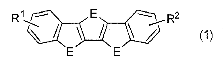
- The compound according to claim 1 wherein all E's in the formula (1) is sulfur atom.
- The compound according to claim 1 or 2 wherein each of R1 and R2 in the formula (1) independently represents a hydrogen atom, an optionally fluorinated C4-30 alkyl group, an optionally fluorinated C4-30 alkoxy group, an optionally alkylated or alkoxylated C6-30 aryl group which is optionally fluorinated, an optionally fluorinated C7-30 aralkyl group, an optionally alkylated or alkoxylated C4-30 heteroaryl group which is optionally fluorinated, or an optionally fluorinated C5-30 heteroaralkyl group.
- The compound according to any one of claims 1 to 3 wherein the compound represented by the formula (1) is a compound represented by the formula (2):

- The compound according to claim 4 wherein, in the formula (2), each E independently represents a sulfur or selenium atom, and each of R1 and R2 independently represents a hydrogen atom, an optionally fluorinated C4-30 alkyl group, or an optionally alkylated or fluorinated C3-30 trialkylsilyl group.
- The compound according to claim 5 wherein each of R1 and R2 in the formula (2) independently represents a C4-30 alkyl group or a C3-30 trialkylsilyl group.
- The compound according to claim 5 wherein R1 and R2 in the formula (2) are C4-30 alkyl groups.
- The compound according to claim 5 wherein R1 and R2 in the formula (2) are the same and represent C4-20 alkyl groups.
- The compound according to claim 5 wherein R1 and R2 in the formula (2) are C6-12 alkyl groups.
- The compound according to claim 4 wherein each of R1 and R2 in the formula (2) independently represents a hydrogen atom, an optionally fluorinated C4-30 alkyl group, an optionally fluorinated C4-30 alkoxy group, an optionally alkylated C6-30 aryl group which is optionally fluorinated, or an optionally fluorinated C7-30 aralkyl group.
- The compound according to claim 4 wherein R1 and R2 in the formula (2) are the same and represent C4-20 alkoxy groups.
- The compound according to claim 4 wherein R1 and R2 in the formula (2) are the same and represent C6-10 aryl groups having C1-20 alkyl groups.
- The compound according to claim 4 wherein R1 and R2 in the formula (2) are the same and represent C7-20 aralkyl groups.
- The compound according to claim 5 wherein each of R1 and R2 in the formula (2) independently represents a C3-30 trialkylsilyl group.
- The compound according to claim 5 wherein each R1 and R2 in the formula (2) independently represents a C3-14 trialkylsilyl group.
- The compound according to claim 4 or 5 wherein R1 and R2 in the formula (2) are the same and represent hexyl or dodecyl.
- The compound according to any one of claims 4 to 16 wherein all E's in the formula (2) are sulfur atoms.
- The compound according to claim 4 wherein all E's in the formula (2) represent sulfur atoms, and R1 and R2 in the formula (2) represent hexyl.
- The compound according to claim 4 wherein all E's in the formula (2) represent sulfur atoms, and R1 and R2 in the formula (2) are the same and represent dodecyl.
- The compound according to claim 4 wherein all E's in the formula (2) represent sulfur atoms, and each of R1 and R2 in the formula (2) independently represents a C6-12 alkyl group.
- A compound represented by the formula [5], [7], [12], [15], [18] or [42] below:


- The compound according to any one of claims 1 to 3 wherein the compound represented by the formula (1) is a compound represented by the formula (3):

- The compound according to claim 22 wherein R1 and R2 in the formula (3) are the same and represent C4-20 alkyl groups.
- A thin film comprising the compound according to any one of claims 1 to 23.
- A thin film consisting of the compound according to any one of claims 1 to 23.
- An organic semiconductor device comprising the thin film according to claim 24 or 25.
- An organic transistor comprising the thin film according to claim 24 or 25.
Applications Claiming Priority (2)
| Application Number | Priority Date | Filing Date | Title |
|---|---|---|---|
| JP2009163919 | 2009-07-10 | ||
| PCT/JP2010/061634 WO2011004869A1 (en) | 2009-07-10 | 2010-07-08 | Substituted benzochalcogenoacene compound, thin film comprising the compound, and organic semiconductor device including the thin film |
Publications (2)
| Publication Number | Publication Date |
|---|---|
| EP2452942A1 true EP2452942A1 (en) | 2012-05-16 |
| EP2452942A4 EP2452942A4 (en) | 2013-01-23 |
Family
ID=43429294
Family Applications (1)
| Application Number | Title | Priority Date | Filing Date |
|---|---|---|---|
| EP10797180A Withdrawn EP2452942A4 (en) | 2009-07-10 | 2010-07-08 | SUBSTITUTED BENZOCHALCOGENOACENE COMPOUND, THIN FILM COMPRISING THE COMPOUND, AND ORGANIC SEMICONDUCTOR DEVICE COMPRISING THE THIN FILM |
Country Status (8)
| Country | Link |
|---|---|
| US (1) | US20120190868A1 (en) |
| EP (1) | EP2452942A4 (en) |
| JP (1) | JP2011032268A (en) |
| KR (1) | KR20120090939A (en) |
| CN (1) | CN102574868B (en) |
| RU (1) | RU2012104635A (en) |
| TW (1) | TW201125871A (en) |
| WO (1) | WO2011004869A1 (en) |
Families Citing this family (15)
| Publication number | Priority date | Publication date | Assignee | Title |
|---|---|---|---|---|
| GB201013820D0 (en) * | 2010-08-18 | 2010-09-29 | Cambridge Display Tech Ltd | Low contact resistance organic thin film transistors |
| KR20140090979A (en) * | 2011-09-12 | 2014-07-18 | 폴리에라 코퍼레이션 | Compounds having semiconducting properties and related compositions and devices |
| GB201116251D0 (en) | 2011-09-20 | 2011-11-02 | Cambridge Display Tech Ltd | Organic semiconductor composition and organic transistor |
| US8372312B1 (en) * | 2011-10-17 | 2013-02-12 | Xerox Corporation | Non-symmetrical dibenzodithienothiophene compounds |
| KR101571590B1 (en) | 2012-11-21 | 2015-11-25 | 주식회사 두산 | Organic compounds and organic electro luminescence device using the same |
| JP2015122383A (en) * | 2013-12-20 | 2015-07-02 | 三星ディスプレイ株式會社Samsung Display Co.,Ltd. | Material for organic electroluminescence device and organic electroluminescence device using the same |
| JP6240544B2 (en) * | 2014-03-28 | 2017-11-29 | 富士フイルム株式会社 | Composition for forming an organic semiconductor film |
| JP2016113434A (en) * | 2014-12-18 | 2016-06-23 | 住友化学株式会社 | Compound, composition comprising the compound and polymer compound, and organic thin film and organic semiconductor element comprising the compound |
| JP6318452B2 (en) * | 2015-01-19 | 2018-05-09 | 富士フイルム株式会社 | Organic thin film transistor and manufacturing method thereof |
| CN104766802B (en) * | 2015-03-26 | 2019-05-03 | 深圳市华星光电技术有限公司 | Liquid crystal display panel, array substrate and manufacturing method of thin film transistor |
| JP6833475B2 (en) * | 2015-12-28 | 2021-02-24 | キヤノン株式会社 | Ink, ink cartridge, and inkjet recording method |
| WO2018061821A1 (en) | 2016-09-29 | 2018-04-05 | 富士フイルム株式会社 | Composition for forming organic semiconductor film, organic semiconductor film and method for producing same, and organic semiconductor element |
| DE102019107163B3 (en) * | 2019-03-20 | 2020-09-10 | Fraunhofer-Gesellschaft zur Förderung der angewandten Forschung e.V. | Thin film transistor and method of making a thin film transistor |
| CN110048025B (en) * | 2019-05-13 | 2022-06-24 | 京东方科技集团股份有限公司 | OLED display screen, display panel and self-assembly packaging method thereof |
| EP4116304A4 (en) * | 2020-03-04 | 2024-03-13 | Tosoh Corporation | AROMATIC COMPOUND, ORGANIC SEMICONDUCTOR LAYER AND ORGANIC THIN FILM TRANSISTOR |
Family Cites Families (7)
| Publication number | Priority date | Publication date | Assignee | Title |
|---|---|---|---|---|
| TWI393724B (en) * | 2004-03-10 | 2013-04-21 | Japan Science & Tech Agency | Condensed polycyclic organic material having chalcogen and method of manufacturing thereof |
| JP5499422B2 (en) * | 2006-06-28 | 2014-05-21 | コニカミノルタ株式会社 | Organic semiconductor material, organic semiconductor film, organic thin film transistor, and organic thin film transistor manufacturing method |
| JP4581062B2 (en) * | 2006-10-20 | 2010-11-17 | 日本化薬株式会社 | Field effect transistor, ink for manufacturing semiconductor device, method for producing field effect transistor, and organic heterocyclic compound |
| JP5134297B2 (en) * | 2007-07-12 | 2013-01-30 | 山本化成株式会社 | Organic transistor |
| JP5141154B2 (en) * | 2007-09-21 | 2013-02-13 | Jnc株式会社 | [1] Benzochalcogeno [3,2-b] [1] Compound having benzochalcogenophene skeleton and organic transistor using the same |
| JP2009152355A (en) * | 2007-12-20 | 2009-07-09 | Konica Minolta Holdings Inc | Organic thin film transistor manufacturing method and organic thin film transistor |
| JP5436811B2 (en) * | 2008-07-31 | 2014-03-05 | 山本化成株式会社 | Organic transistor |
-
2010
- 2010-07-08 RU RU2012104635/04A patent/RU2012104635A/en unknown
- 2010-07-08 WO PCT/JP2010/061634 patent/WO2011004869A1/en not_active Ceased
- 2010-07-08 US US13/382,821 patent/US20120190868A1/en not_active Abandoned
- 2010-07-08 KR KR1020127003557A patent/KR20120090939A/en not_active Withdrawn
- 2010-07-08 EP EP10797180A patent/EP2452942A4/en not_active Withdrawn
- 2010-07-08 JP JP2010156017A patent/JP2011032268A/en active Pending
- 2010-07-08 CN CN201080040263.5A patent/CN102574868B/en not_active Expired - Fee Related
- 2010-07-09 TW TW099122671A patent/TW201125871A/en unknown
Non-Patent Citations (2)
| Title |
|---|
| No further relevant documents disclosed * |
| See also references of WO2011004869A1 * |
Also Published As
| Publication number | Publication date |
|---|---|
| KR20120090939A (en) | 2012-08-17 |
| RU2012104635A (en) | 2013-08-20 |
| JP2011032268A (en) | 2011-02-17 |
| WO2011004869A1 (en) | 2011-01-13 |
| EP2452942A4 (en) | 2013-01-23 |
| CN102574868B (en) | 2015-01-14 |
| TW201125871A (en) | 2011-08-01 |
| US20120190868A1 (en) | 2012-07-26 |
| CN102574868A (en) | 2012-07-11 |
Similar Documents
| Publication | Publication Date | Title |
|---|---|---|
| US20120190868A1 (en) | Substituted benzochalcogenoacene compound, thin film comprising the compound, and organic semiconductor device including the thin film | |
| JP5581596B2 (en) | Organic semiconductor materials | |
| CN105102462B (en) | Organic compound containing oxygen group element, its production method and use | |
| CN104125951B (en) | Chalcogen-containing organic compound and method for producing same, organic semiconductor material, organic semiconductor film, and organic field-effect transistor | |
| US9133211B2 (en) | Dithienobenzodithiophene semiconductive material and electronic device using the same | |
| US7956199B2 (en) | Methods for preparing benzodithiophenes | |
| CN105837597B (en) | Fused polycyclic heteroaromatic compound, organic thin film comprising said compound, and electronic device comprising organic thin film | |
| TWI549327B (en) | Organic field effect transistor and organic semiconductor material | |
| WO2010027106A1 (en) | Novel compound and organic semiconductor material | |
| KR101890723B1 (en) | Semiconductor composition | |
| JP2013534213A (en) | Semiconductors based on substituted [1] benzothieno [3,2-b] [1] -benzothiophene | |
| EP3697780B1 (en) | New substituted benzonaphthathiophene compounds for organic electronics | |
| EP3902023B1 (en) | Composition containing organic semiconductor, solution for forming organic semiconductor layer, organic semiconductor layer, and organic thin film transistor | |
| WO2008120839A1 (en) | Novel organic semiconductor compound, and organic thin film transistor using the same | |
| EP2511278A1 (en) | Thienopyrazine compound and field effect transistor containing same | |
| US20230142592A1 (en) | Aromatic compound, organic semiconductor layer and organic thin film transistor | |
| JP4955918B2 (en) | Asymmetric linear organic oligomer and production method and use thereof | |
| KR100865703B1 (en) | Organic Semiconductor Compound of Arylacetylene Structure and Organic Thin Film Transistor Using the Same | |
| Choi et al. | Synthesis and characterization of a series of bis (dimethyl-n-octylsilyl) oligothiophenes for organic thin film transistor applications | |
| JP7317301B2 (en) | Organic semiconductor compound and its use | |
| EP3845525B1 (en) | Chalcogen-containing organic compound, organic semiconductor material, organic semiconductor film, and organic field-effect transistor | |
| JPWO2011071017A1 (en) | Diazaborol compound and field effect transistor containing the same | |
| KR20120078051A (en) | Organic semiconductor having asymmetric structure, and organic thin film transistor using the same | |
| WO2012111533A1 (en) | Compound for organic transistor | |
| WO2012096360A1 (en) | Substituted benzochalcogenoacene compound |
Legal Events
| Date | Code | Title | Description |
|---|---|---|---|
| PUAI | Public reference made under article 153(3) epc to a published international application that has entered the european phase |
Free format text: ORIGINAL CODE: 0009012 |
|
| 17P | Request for examination filed |
Effective date: 20120201 |
|
| AK | Designated contracting states |
Kind code of ref document: A1 Designated state(s): AL AT BE BG CH CY CZ DE DK EE ES FI FR GB GR HR HU IE IS IT LI LT LU LV MC MK MT NL NO PL PT RO SE SI SK SM TR |
|
| DAX | Request for extension of the european patent (deleted) | ||
| A4 | Supplementary search report drawn up and despatched |
Effective date: 20121220 |
|
| RIC1 | Information provided on ipc code assigned before grant |
Ipc: H01L 51/30 20060101ALI20121214BHEP Ipc: C07D 495/14 20060101AFI20121214BHEP Ipc: H01L 51/05 20060101ALI20121214BHEP Ipc: H01L 29/786 20060101ALI20121214BHEP |
|
| STAA | Information on the status of an ep patent application or granted ep patent |
Free format text: STATUS: THE APPLICATION IS DEEMED TO BE WITHDRAWN |
|
| 18D | Application deemed to be withdrawn |
Effective date: 20130719 |