EP2451071A1 - Control method for converting power, and electronic power converter adapted to carry out said method - Google Patents
Control method for converting power, and electronic power converter adapted to carry out said method Download PDFInfo
- Publication number
- EP2451071A1 EP2451071A1 EP11382315A EP11382315A EP2451071A1 EP 2451071 A1 EP2451071 A1 EP 2451071A1 EP 11382315 A EP11382315 A EP 11382315A EP 11382315 A EP11382315 A EP 11382315A EP 2451071 A1 EP2451071 A1 EP 2451071A1
- Authority
- EP
- European Patent Office
- Prior art keywords
- alternating voltage
- additional
- waves
- inverters
- voltage waveform
- Prior art date
- Legal status (The legal status is an assumption and is not a legal conclusion. Google has not performed a legal analysis and makes no representation as to the accuracy of the status listed.)
- Granted
Links
- 238000000034 method Methods 0.000 title claims abstract description 38
- 230000016507 interphase Effects 0.000 claims description 7
- 238000006243 chemical reaction Methods 0.000 claims description 4
- 230000008030 elimination Effects 0.000 claims description 3
- 238000003379 elimination reaction Methods 0.000 claims description 3
- 230000000903 blocking effect Effects 0.000 claims description 2
- 230000000116 mitigating effect Effects 0.000 claims 1
- 230000008878 coupling Effects 0.000 description 12
- 238000010168 coupling process Methods 0.000 description 12
- 238000005859 coupling reaction Methods 0.000 description 12
- 230000005540 biological transmission Effects 0.000 description 11
- 239000004065 semiconductor Substances 0.000 description 7
- 230000001965 increasing effect Effects 0.000 description 6
- 238000004804 winding Methods 0.000 description 4
- 238000005516 engineering process Methods 0.000 description 3
- 230000001939 inductive effect Effects 0.000 description 2
- 238000002623 insulin potentiation therapy Methods 0.000 description 2
- 230000003068 static effect Effects 0.000 description 2
- 239000003990 capacitor Substances 0.000 description 1
- 238000006073 displacement reaction Methods 0.000 description 1
- 238000002347 injection Methods 0.000 description 1
- 239000007924 injection Substances 0.000 description 1
- 238000004519 manufacturing process Methods 0.000 description 1
- 239000000243 solution Substances 0.000 description 1
- 230000001360 synchronised effect Effects 0.000 description 1
Images


Classifications
-
- H—ELECTRICITY
- H02—GENERATION; CONVERSION OR DISTRIBUTION OF ELECTRIC POWER
- H02M—APPARATUS FOR CONVERSION BETWEEN AC AND AC, BETWEEN AC AND DC, OR BETWEEN DC AND DC, AND FOR USE WITH MAINS OR SIMILAR POWER SUPPLY SYSTEMS; CONVERSION OF DC OR AC INPUT POWER INTO SURGE OUTPUT POWER; CONTROL OR REGULATION THEREOF
- H02M7/00—Conversion of ac power input into dc power output; Conversion of dc power input into ac power output
- H02M7/42—Conversion of dc power input into ac power output without possibility of reversal
- H02M7/44—Conversion of dc power input into ac power output without possibility of reversal by static converters
- H02M7/48—Conversion of dc power input into ac power output without possibility of reversal by static converters using discharge tubes with control electrode or semiconductor devices with control electrode
- H02M7/483—Converters with outputs that each can have more than two voltages levels
- H02M7/49—Combination of the output voltage waveforms of a plurality of converters
-
- H—ELECTRICITY
- H02—GENERATION; CONVERSION OR DISTRIBUTION OF ELECTRIC POWER
- H02M—APPARATUS FOR CONVERSION BETWEEN AC AND AC, BETWEEN AC AND DC, OR BETWEEN DC AND DC, AND FOR USE WITH MAINS OR SIMILAR POWER SUPPLY SYSTEMS; CONVERSION OF DC OR AC INPUT POWER INTO SURGE OUTPUT POWER; CONTROL OR REGULATION THEREOF
- H02M1/00—Details of apparatus for conversion
- H02M1/0083—Converters characterised by their input or output configuration
- H02M1/009—Converters characterised by their input or output configuration having two or more independently controlled outputs
-
- H—ELECTRICITY
- H02—GENERATION; CONVERSION OR DISTRIBUTION OF ELECTRIC POWER
- H02M—APPARATUS FOR CONVERSION BETWEEN AC AND AC, BETWEEN AC AND DC, OR BETWEEN DC AND DC, AND FOR USE WITH MAINS OR SIMILAR POWER SUPPLY SYSTEMS; CONVERSION OF DC OR AC INPUT POWER INTO SURGE OUTPUT POWER; CONTROL OR REGULATION THEREOF
- H02M7/00—Conversion of ac power input into dc power output; Conversion of dc power input into ac power output
- H02M7/42—Conversion of dc power input into ac power output without possibility of reversal
- H02M7/44—Conversion of dc power input into ac power output without possibility of reversal by static converters
- H02M7/48—Conversion of dc power input into ac power output without possibility of reversal by static converters using discharge tubes with control electrode or semiconductor devices with control electrode
- H02M7/483—Converters with outputs that each can have more than two voltages levels
- H02M7/487—Neutral point clamped inverters
Definitions
- This invention relates to control methods in high-power environments, and in particular to control methods for converting energy for transmission and/or distribution lines from a Dc voltage.
- the invention also relates to electronic power converters adapted to carry out said control methods.
- Electronic power converters are currently used in a wide range of applications where a DC/AC conversion is required, carried out by means of inverters comprised by said converters, such as variable-speed drives, variable-speed wind turbines, solar inverters, UPS systems (Uninterruptible Power Supplies) or FACTS devices (Flexible AC Transmission Systems).
- inverters comprised by said converters, such as variable-speed drives, variable-speed wind turbines, solar inverters, UPS systems (Uninterruptible Power Supplies) or FACTS devices (Flexible AC Transmission Systems).
- Inverters in electronic power converters comprise static semiconductor-type switches.
- the switching characteristics of the semiconductor devices currently available on the market enable the most suitable semiconductor for each type of application to be chosen.
- different families of semiconductors may be identified:
- the output voltage of the converter can be increased by increasing the number of levels of its output voltage, thereby increasing the power of the converter, which is achieved by using multi-level inverters.
- the quality of the waveform of the output voltage increases with the number of levels.
- a three-level inverter for example, it is possible to obtain a five-level output voltage waveform.
- the greater the number of levels the greater the complexity in implementing the converter (of the inverters), as a result of which, and generally speaking, industrial applications are usually based on inverters or branches of up to two or three levels at most.
- Document US 5889668 A discloses an electronic power converter.
- Dc voltage is converted into alternating voltage obtaining different alternating voltage waves by means of different inverters, a plurality of alternating output voltage waves being obtained.
- Said alternating output voltage waves are combined in parallel in twos, by means of interphase transformers or IPTs, until two resulting alternating voltage waves are obtained and which are handled for the elimination of at least some of their harmonics.
- the two resulting alternating voltage waves then reach two secondary windings of a coupling transformer by means of which the electronic power converter is coupled to the transmission and/or distribution line.
- the windings of one secondary are connected in wye and the windings of the other secondary in delta.
- a DC voltage is converted into alternating voltage for obtaining at least one first alternating voltage waveform by means of at least one inverter and a second alternating voltage waveform by means of at least one other inverter, and the alternating output voltage waves of both inverters are combined in parallel, a high-power resulting alternating voltage waveform thus being obtained.
- an additional resulting alternating voltage waveform is also generated, a third alternating voltage waveform by means of at least one additional inverter and a fourth alternating voltage waveform by means of at least one other inverter being obtained during the conversion, and the alternating output voltage waves of said additional inverters are combined in parallel.
- the additional resulting alternating voltage waveform is phase-shifted by approximately 180° in relation to the resulting alternating voltage waveform, so that thanks to the control method of the invention two voltage signals are generated and which are adapted to correspond with two output signals of the converter (voltage waves in two terminals of said converter), said terminals being used to couple the converter to a load (preferably the load corresponds with a transmission and/or distribution line).
- the voltage waves of the two terminals that are used to couple the converter to a load are substantially in opposition, the voltage of the output voltage waveform of said converter is also practically doubled, thereby providing a high-power converter in a simple and economic manner, without the need for additional elements that would make said converter more expensive.
- two voltage waves are obtained and are adapted to be supplied through two terminals of the converter, enabling a converter with two open poles on the output to be coupled to a load (preferably the load corresponds with a transmission and/or distribution line), generally by means of a specific magnetic component.
- said magnetic component can comprise a coupling transformer with a single coil on the secondary, where the two terminals of the converter are connected, so that an electronic power converter with less magnetic components than those necessary in the prior art is obtained and, therefore, a more economical converter, and also with a reduction in the associated high-voltage switchgear necessary, which would involve a very high cost. This implies a reduction in the size of the magnetic components that are used, which results in a smaller size of the converter, which can be advantageous in some situations.
- the common-mode voltages are also eliminated in an ordinary manner from at least one of the alternating voltage waves, as a result of which the quality of the voltage waveform applied in the load is optimal, the low number of inverters being used, which implies a reduction in the cost and the size of the resulting converter in relation to those used in the prior art.
- This also allows the use of modulation techniques that produce a zero-sequence voltage component, for the purposes of increasing the voltage of the output voltage waveform and, i. e. the power supplied by the converter, in a simple manner.
- the control method of the invention is adapted for its use in electronic power converters C, in particular of the VSC type (Voltage Source Converter), which convert DC voltage into alternating voltage preferably for transmission and/or distribution lines.
- VSC Voltage Source Converter
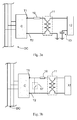
- FIG. 1 in the form of blocks, shows an embodiment of an electronic power converter C adapted to support the method of the invention.
- Said converter C comprises at least one first three-phase inverter 1 that is fed by DC voltage from a DC power supply, and at least one second three-phase inverter 2 that is also fed by said DC voltage, the DC voltage being converted into a first alternating voltage waveform AC1 by means of the first inverter 1, and in a second alternating voltage waveform AC2 by means of the second inverter 2.
- the converter C also comprises combination means 9 that preferably correspond with an interphase transformer or IPT (interphase transformer), to combine in parallel said alternating voltage waves AC1 and AC2 with each other, a resulting alternating voltage waveform AC12 being obtained.
- IPT interphase transformer
- said alternating voltage waves AC1 and AC2 of the inverters 1 and 2 are displaced in phase by a small angle ⁇ in relation to each other so that, by slightly sacrificing the amplitude of the resulting alternating output voltage waveform AC12, certain harmonics of said alternating voltage waveform AC12 are eliminated or reduced.
- Said angle ⁇ can be approximately 7.5°, for example, an angle at which the harmonics close to twenty-four in the resulting waveform are eliminated or reduced, in other words harmonics twenty-three and twenty-five are reduced to such an extent they can be considered eliminated, with an insignificant reduction of the amplitude of said resulting alternating output voltage waveform AC12.
- the converter C also comprises at least one third inverter 3 and one fourth inverter 4 fed by the DC voltage, a first additional alternating voltage waveform AC3 and a second additional alternating voltage waveform AC4 being obtained respectively as a result of the conversion.
- Said converter C comprises additional combination means 10, which preferably correspond with an interphase transformer or IPT, to combine in parallel said additional alternating voltage waves AC3 and AC4 with each other, with a resulting additional alternating voltage AC34 being obtained.
- Both resulting alternating voltage waves AC12 and AC34 are supplied to the output of the converter C by means of two terminals T1 and T2 of the converter C, thereby enabling a converter C with two poles or terminals T1 and T2 open at the output to be coupled to a load 12 (preferably the load corresponds with a transmission and/or distribution line), by means of a specific magnetic component 11 as shown in the embodiment of Figure 3a , referring to a parallel coupling to the load 12, and in the embodiment of Figure 3b , referring to a series coupling to the load 12.
- Said magnetic component 11 comprises a three-phase coupling transformer with a single coil in the secondary, where the two terminals T1 and T2 of the converter C are connected, so that the coupling in series to the load 12 is made easier and an electronic power converter C with less magnetic components than those necessary in the prior art is obtained and, therefore, a more economical converter.
- Said coupling transformer can also comprise an auxiliary delta winding that provides a low-impedance path for the zero-sequence currents. As a result, the zero-sequence currents that flow along the line do not flow through the converter and vice versa. Additionally, this involves a reduction of the size of the magnetic components that are used, which involves a smaller size of the unit formed by the converter C and said magnetic components.
- a capacitor bank 13 is generally used to increase the capacitive power, and an additional reactance 19 to increase the inductive power of the equipment and reduce short-circuit intensity through a secondary of the coupling transformer, whereas in the series coupling an additional reactance 18 is generally used to increase the inductive power of the equipment and reduce short-circuit intensity through a secondary of the coupling transformer, and a by-pass 17 to close it in the event of a fault in the load.
- the additional resulting alternating voltage waveform AC34 is displaced in phase approximately 180° in relation to the resulting alternating voltage waveform AC12, so that the output voltage waveform of the converter C is also increased when it is coupled to the load 12.
- the inverters 1, 2, 3 and 4 used are multi-level inverters, preferably of three levels such as the one shown in Figure 4 (hence the alternating voltage waves AC1 and AC2 shown in Figure 2 ), which enables the output power of the converter C to be increased.
- the system is three-phase, as a result of which the inverters used are also three-phase and generate three output phases F1, F2 and F3 (the alternating voltage waves AC1, AC2, AC3 and AC4 correspond with one of said phases F1, F2 or F3, for which reason, as commented above, only one phase is detailed in a single-wire manner for purposes of clarity).
- the converter C comprises filter means 7, 8, which preferably correspond with a zero-sequence blocking transformer or ZSBT.
- said common-mode voltages are eliminated once the resulting alternating voltage waves AC12 and AC34 have been obtained, a single ZSBT thus being used for each terminal T1 and T2 of the converter C as shown in the embodiment of Figure 1 , though they can also be eliminated in the step prior to the obtaining of said resulting alternating voltage waves AC12 and AC34, before the alternating voltage waves AC1 and AC2; AC3 and AC4 are combined with each other, as a result of which said voltages are eliminated directly from said alternating voltage waves AC1 and AC2; AC3 and AC4, a ZSBT being used for each of them.
- PWM modulation Pulse Width Modulation
- the shape of the output waveform is obtained by comparing an modulated output waveform (for instance at a frequency of 50Hz) with a high-frequency triangular waveform (for instance 600 - 10,000 Hz), an output voltage waveform of low harmonic content being obtained.
- Said PWM modulation may be carried out by using the respective modulating waves M1 and M2 displaced in phase in relation to each other, in both inverters 1 and 2; 3 and 4 whose alternating output voltage waves AC1 and AC2; AC3 and AC4 are combined in parallel, and the triangular waves 21 and 22 that are equal and in phase, as shown in Figure 5 , or with the modulating waves M1 and M2 in phase and the triangular waves 21 and 22 equal but displaced in phase in relation to each other, preferably by approximately 90°.
- a combination of the two can also be adopted, in other words, displaced in phase carrier and modulating waves.
- Similar output voltage waves can be obtained by alternative means, for example, by using vectorial modulation techniques of the SVPWM (Space Vector Pulse-Width Modulation) type.
- SVPWM Space Vector Pulse-Width Modulation
- This arrangement also enables the injection of zero-sequence harmonics, for example, the third, to increase the output voltage, as it is blocked by the ZSBT(s).
- a second embodiment of the method of the invention selective harmonic elimination or SHE modulation techniques are used, and by means of which the phase displacements of the switching signals to the semiconductors of the different inverters 1, 2, 3 and 4 are controlled, the two fundamental waves of the different inverters 1 and 2; 3 and 4 whose alternating output voltage waves AC1 and AC2; AC3 and AC4 are combined in parallel being in phase or otherwise.
- certain harmonics of the alternating voltage waves AC1, AC2, AC3 and AC4 are eliminated or reduced, which results in a reduction of the harmonic content of said alternating voltage waves AC1, AC2, AC3 and AC4.
Abstract
Description
- This invention relates to control methods in high-power environments, and in particular to control methods for converting energy for transmission and/or distribution lines from a Dc voltage. The invention also relates to electronic power converters adapted to carry out said control methods.
- Electronic power converters are currently used in a wide range of applications where a DC/AC conversion is required, carried out by means of inverters comprised by said converters, such as variable-speed drives, variable-speed wind turbines, solar inverters, UPS systems (Uninterruptible Power Supplies) or FACTS devices (Flexible AC Transmission Systems).
- Inverters in electronic power converters comprise static semiconductor-type switches. The switching characteristics of the semiconductor devices currently available on the market enable the most suitable semiconductor for each type of application to be chosen. As a result, depending on the power level required or demanded, different families of semiconductors may be identified:
- MOSFETs: These are FET-technology semiconductors, ideal for low power/voltage and high-frequency-switching applications, such as switched sources and photovoltaic inverters. They are the most widely used in mass-produced consumer appliances.
- IGBTs and IEGTs: Transistor-technology semiconductors. The IGBT has become the standard in low- and mid-power applications and in multi-MW applications with multi-level topologies. Mitsubishi has recently developed the IEGT with encapsulated press-pack for mid-voltage and high-power applications, as a result of which three-phase inverters of up to 10MVAs can now be made. These are used in industrial drives, electric rail traction and equipment for renewable-energy generators (solar and wind), for example.
- GTOs and IGCTs: Thyristor-technology semiconductors, provided with drivers that enable them to operate with forced switching. As with IEGTs, converters with power units of approximately 10MW can be developed, although the switching frequency is limited to frequencies in the region of 200Hz for GTOs and 1000Hz for IGCTs. They may be applied, for example, in high-power drives, FACTS devices, which may typically be SSSC (Static Series Synchronous Compensator) if connected in series with a transmission and/or distribution line, or STATCOM if connected in parallel with a transmission and/or distribution line, or UPFC (Universal Power Flow Controller), this being a combination of SSSC and STATCOM.
- The output voltage of the converter can be increased by increasing the number of levels of its output voltage, thereby increasing the power of the converter, which is achieved by using multi-level inverters. In addition, the quality of the waveform of the output voltage increases with the number of levels. As a result, with a three-level inverter, for example, it is possible to obtain a five-level output voltage waveform. The greater the number of levels, the greater the complexity in implementing the converter (of the inverters), as a result of which, and generally speaking, industrial applications are usually based on inverters or branches of up to two or three levels at most.
- The most commonly used solution in the manufacture of high-power converters for FACTS applications, for example, is the connection of three-phase inverters of two or three levels to each other by means of intermediate magnetic elements or transformers, so that thanks to said connection or combination, another increase in the output voltage, and, therefore, in the power of the converter, is achieved, also improving the quality of the output waveform. For example, document
US 3628123 A discloses the combination in parallel of two inverters by means of interphase transformers or IPTs ("Interphase transformer"). - Document
US 5889668 A discloses an electronic power converter. In said converter Dc voltage is converted into alternating voltage obtaining different alternating voltage waves by means of different inverters, a plurality of alternating output voltage waves being obtained. Said alternating output voltage waves are combined in parallel in twos, by means of interphase transformers or IPTs, until two resulting alternating voltage waves are obtained and which are handled for the elimination of at least some of their harmonics. The two resulting alternating voltage waves then reach two secondary windings of a coupling transformer by means of which the electronic power converter is coupled to the transmission and/or distribution line. To reduce the harmonic content of the voltage in the primary of the coupling transformer, the windings of one secondary are connected in wye and the windings of the other secondary in delta. - It is an object of the invention to provide a method for converting DC voltage into alternating voltage for transmission and/or distribution lines. It is another object of the invention to provide a converter adapted to carry out said method, in order that the power supplied to the transmission and/or distribution lines comprises a high voltage value while also presenting optimal waveform quality.
- In the method of the invention a DC voltage is converted into alternating voltage for obtaining at least one first alternating voltage waveform by means of at least one inverter and a second alternating voltage waveform by means of at least one other inverter, and the alternating output voltage waves of both inverters are combined in parallel, a high-power resulting alternating voltage waveform thus being obtained.
- In addition, thanks to the method of the invention, an additional resulting alternating voltage waveform is also generated, a third alternating voltage waveform by means of at least one additional inverter and a fourth alternating voltage waveform by means of at least one other inverter being obtained during the conversion, and the alternating output voltage waves of said additional inverters are combined in parallel.
- The additional resulting alternating voltage waveform is phase-shifted by approximately 180° in relation to the resulting alternating voltage waveform, so that thanks to the control method of the invention two voltage signals are generated and which are adapted to correspond with two output signals of the converter (voltage waves in two terminals of said converter), said terminals being used to couple the converter to a load (preferably the load corresponds with a transmission and/or distribution line). As a result, as the voltage waves of the two terminals that are used to couple the converter to a load are substantially in opposition, the voltage of the output voltage waveform of said converter is also practically doubled, thereby providing a high-power converter in a simple and economic manner, without the need for additional elements that would make said converter more expensive.
- Thanks to the control method of the invention two voltage waves are obtained and are adapted to be supplied through two terminals of the converter, enabling a converter with two open poles on the output to be coupled to a load (preferably the load corresponds with a transmission and/or distribution line), generally by means of a specific magnetic component. Thanks to the arrangement of converter allowed by the method of the invention, said magnetic component can comprise a coupling transformer with a single coil on the secondary, where the two terminals of the converter are connected, so that an electronic power converter with less magnetic components than those necessary in the prior art is obtained and, therefore, a more economical converter, and also with a reduction in the associated high-voltage switchgear necessary, which would involve a very high cost. This implies a reduction in the size of the magnetic components that are used, which results in a smaller size of the converter, which can be advantageous in some situations.
- With the method of the invention the common-mode voltages are also eliminated in an ordinary manner from at least one of the alternating voltage waves, as a result of which the quality of the voltage waveform applied in the load is optimal, the low number of inverters being used, which implies a reduction in the cost and the size of the resulting converter in relation to those used in the prior art. This also allows the use of modulation techniques that produce a zero-sequence voltage component, for the purposes of increasing the voltage of the output voltage waveform and, i. e. the power supplied by the converter, in a simple manner.
- The same advantages explained for the method can also be applied to the converter of the invention.
- These and other advantages and characteristics of the invention will be made evident in the light of the drawings and the detailed description thereof.
-
-
Figure 1 schematically shows an embodiment of an electronic power converter of the invention. -
Figure 2 shows the alternating output voltages of two inverters of the converter of -
Figure 1 , which are combined in parallel with each other. -
Figure 3a schematically shows a converter according toFigure 1 , coupled to a load in parallel by means of a magnetic component. -
Figure 3b schematically shows a converter according toFigure 1 , coupled to a load in series by means of a magnetic component. -
Figure 4 shows a multi-level inverter of the converter ofFigure 1 . -
Figure 5 shows waves used in a PWM-modulation embodiment, in an embodiment of the method of the invention implemented in the converter ofFigure 1 . - The control method of the invention is adapted for its use in electronic power converters C, in particular of the VSC type (Voltage Source Converter), which convert DC voltage into alternating voltage preferably for transmission and/or distribution lines. Although it is a three-phase system, the Figures and the description show and explain the invention in a single-wire manner for the purposes of clarity.
-
Figure 1 , in the form of blocks, shows an embodiment of an electronic power converter C adapted to support the method of the invention. Said converter C comprises at least one first three-phase inverter 1 that is fed by DC voltage from a DC power supply, and at least one second three-phase inverter 2 that is also fed by said DC voltage, the DC voltage being converted into a first alternating voltage waveform AC1 by means of thefirst inverter 1, and in a second alternating voltage waveform AC2 by means of thesecond inverter 2. The converter C also comprises combination means 9 that preferably correspond with an interphase transformer or IPT (interphase transformer), to combine in parallel said alternating voltage waves AC1 and AC2 with each other, a resulting alternating voltage waveform AC12 being obtained. Preferably, as shown inFigure 2 , said alternating voltage waves AC1 and AC2 of theinverters - In order to carry out the method of the invention, the converter C also comprises at least one
third inverter 3 and onefourth inverter 4 fed by the DC voltage, a first additional alternating voltage waveform AC3 and a second additional alternating voltage waveform AC4 being obtained respectively as a result of the conversion. Said converter C comprises additional combination means 10, which preferably correspond with an interphase transformer or IPT, to combine in parallel said additional alternating voltage waves AC3 and AC4 with each other, with a resulting additional alternating voltage AC34 being obtained. Both resulting alternating voltage waves AC12 and AC34 are supplied to the output of the converter C by means of two terminals T1 and T2 of the converter C, thereby enabling a converter C with two poles or terminals T1 and T2 open at the output to be coupled to a load 12 (preferably the load corresponds with a transmission and/or distribution line), by means of a specificmagnetic component 11 as shown in the embodiment ofFigure 3a , referring to a parallel coupling to theload 12, and in the embodiment ofFigure 3b , referring to a series coupling to theload 12. Saidmagnetic component 11 comprises a three-phase coupling transformer with a single coil in the secondary, where the two terminals T1 and T2 of the converter C are connected, so that the coupling in series to theload 12 is made easier and an electronic power converter C with less magnetic components than those necessary in the prior art is obtained and, therefore, a more economical converter. Said coupling transformer can also comprise an auxiliary delta winding that provides a low-impedance path for the zero-sequence currents. As a result, the zero-sequence currents that flow along the line do not flow through the converter and vice versa. Additionally, this involves a reduction of the size of the magnetic components that are used, which involves a smaller size of the unit formed by the converter C and said magnetic components. In the parallel coupling acapacitor bank 13 is generally used to increase the capacitive power, and anadditional reactance 19 to increase the inductive power of the equipment and reduce short-circuit intensity through a secondary of the coupling transformer, whereas in the series coupling anadditional reactance 18 is generally used to increase the inductive power of the equipment and reduce short-circuit intensity through a secondary of the coupling transformer, and a by-pass 17 to close it in the event of a fault in the load. - In the embodiment of
Figure 1 and throughout the description mention is made of the use of fourinverters Figure 1 and the description. - The additional resulting alternating voltage waveform AC34 is displaced in phase approximately 180° in relation to the resulting alternating voltage waveform AC12, so that the output voltage waveform of the converter C is also increased when it is coupled to the
load 12. Theinverters Figure 4 (hence the alternating voltage waves AC1 and AC2 shown inFigure 2 ), which enables the output power of the converter C to be increased. As commented, the system is three-phase, as a result of which the inverters used are also three-phase and generate three output phases F1, F2 and F3 (the alternating voltage waves AC1, AC2, AC3 and AC4 correspond with one of said phases F1, F2 or F3, for which reason, as commented above, only one phase is detailed in a single-wire manner for purposes of clarity). - Thanks to the method the common-mode voltages of at least one of the alternating voltage waves AC1, AC2, AC3, AC4, AC12 or AC34 are also eliminated, which involves a reduction in the harmonic content of the output voltage waveform of the converter C, as a result of which the quality of the voltage and/or power supplied to the
load 12 is optimal. For this purpose the converter C comprises filter means 7, 8, which preferably correspond with a zero-sequence blocking transformer or ZSBT. Preferably, said common-mode voltages are eliminated once the resulting alternating voltage waves AC12 and AC34 have been obtained, a single ZSBT thus being used for each terminal T1 and T2 of the converter C as shown in the embodiment ofFigure 1 , though they can also be eliminated in the step prior to the obtaining of said resulting alternating voltage waves AC12 and AC34, before the alternating voltage waves AC1 and AC2; AC3 and AC4 are combined with each other, as a result of which said voltages are eliminated directly from said alternating voltage waves AC1 and AC2; AC3 and AC4, a ZSBT being used for each of them. Only one ZSBT can also be used for one of the resulting voltage waves AC12 or AC34 of one of said terminals T1 or T2, and none used in the other terminal T2 or T1. Instead of one of these alternative proposals a combination of them can also be adopted, provided that it is used to eliminate the common-mode voltages. As a result, and in addition, thanks to the method of the invention, as a few number ofinverters - To reduce the harmonic content of the output voltage to be supplied to the
load 12, in a first embodiment of the method of the invention PWM modulation (Pulse Width Modulation) type techniques are used, in which the shape of the output waveform is obtained by comparing an modulated output waveform (for instance at a frequency of 50Hz) with a high-frequency triangular waveform (for instance 600 - 10,000 Hz), an output voltage waveform of low harmonic content being obtained. Said PWM modulation may be carried out by using the respective modulating waves M1 and M2 displaced in phase in relation to each other, in bothinverters triangular waves Figure 5 , or with the modulating waves M1 and M2 in phase and thetriangular waves - To reduce the harmonic content of the output voltage, in a second embodiment of the method of the invention selective harmonic elimination or SHE modulation techniques are used, and by means of which the phase displacements of the switching signals to the semiconductors of the
different inverters different inverters
Claims (15)
- Control method for converting power, wherein
DC voltage is converted into alternating voltage, at least one first alternating voltage waveform (AC1) being obtained by means of at least one multi-level inverter (1), and one second alternating voltage waveform (AC2) being obtained by means of at least one other multi-level inverter (2), and wherein
the alternating voltage waves (AC1, AC2) of the different inverters (1, 2) are combined in parallel a resulting alternating voltage waveform (AC12) being obtained,
characterised in that
during the conversion of DC voltage into alternating voltage an additional alternating voltage waveform (AC3) is obtained by means of at least one additional multi-level inverter (3) and a second additional alternating voltage waveform (AC4) is obtained by means of at least one other additional multi-level inverter (4), said additional alternating voltage waves (AC3, AC4) being combined in parallel an additional resulting alternating voltage waveform (AC34) being obtained as a result of the combination, the additional resulting alternating voltage waveform (AC34) being displaced in phase by approximately 180° in relation to the resulting alternating voltage waveform (AC12), and
the common-mode voltages are eliminated from at least one of the alternating voltage waves (AC1, AC2; AC12; AC3, AC4; AC34). - Method according to claim 1, wherein the alternating voltage waves (AC1, AC2; AC3, AC4) that are combined in parallel with each other to obtain the corresponding resulting alternating voltage waveform (AC12; AC34) comprise different instantaneous values.
- Method according to claim 2, wherein in order to convert DC voltage into alternating voltage for obtaining the alternating voltage waves (AC1, AC2; AC3, AC4), the inverters (1, 2; 3, 4) use a PWM modulation with modulating signals in both inverters (1, 2; 3, 4) displaced in phase in respect to each other, and triangular carrier signals that are in phase.
- Method according to claim 2, wherein in order to convert DC voltage into alternating voltage for obtaining the alternating voltage waves (AC1, AC2; AC3, AC4), the inverters (1, 2; 3, 4) use a PWM modulation with modulating signals in both inverters (1, 2; 3, 4) in phase, and triangular carrier signals that are equal but displaced in phase in relation to each other.
- Method according to claim 2, wherein in order to convert DC voltage into alternating voltage for obtaining the alternating voltage waves (AC1, AC2; AC3, AC4), the inverters (1, 2; 3, 4) use a PWM modulation with modulating signals in both inverters (1, 2; 3, 4) displaced in phase a certain angle in relation to each other, and triangular carrier signals that are equal but displaced in phase in relation to each other.
- Method according to claim 2, wherein in order to convert DC voltage (DC1; DC2) into alternating voltage for obtaining the alternating voltage waves (AC1; AC2) a selective harmonic elimination or mitigation modulation is used.
- Method according to any of the preceding claims, wherein the common-mode voltages are eliminated from at least one of the alternating voltage waves (AC1, AC2; AC12) and/or one of the additional alternating voltage waves (AC3, AC4; AC34).
- Method according to any of the preceding claims, wherein the common-mode voltages are eliminated from the alternating voltage waves (AC1, AC2; AC3, AC4) once said alternating voltage waves (AC1, AC2; AC3, AC4) have been combined.
- Method according to any of claims 1 to 6, wherein the common-mode voltage is eliminated from each alternating voltage waveform (AC1, AC2; AC3, AC4), said alternating voltage waves (AC1, AC2; AC3, AC4) subsequently being combined with each other.
- Electronic power converter adapted to carry out the control method according to any of the preceding claims, comprising
a block (B1) of inverters that comprises at least two multi-level inverters (1, 2) to convert DC voltage into alternating voltage at least two alternating voltage waveform (AC1, AC2) being obtained, and
combination means (9) for combining in parallel both alternating voltage waves (AC1, AC2), a resulting alternating voltage waveform (AC12) being obtained as a result of the combination,
characterised in that
the converter also comprises an additional block (B2) of inverters that comprises at least two additional multi-level inverters (3, 4) to convert Dc voltage(DC) into alternating voltage at least two additional alternating voltage waves (AC3, AC4),
additional combination means (10) to combine in parallel both additional alternating voltage waves (AC3, AC4), an additional resulting alternating voltage waveform (AC34) displaced in phase by approximately 180° with the resulting alternating voltage waveform (AC12) being generated, and
filter means (7; 8) to eliminate the common-mode voltages from the alternating voltage waves (AC1, AC2; AC12; AC2, AC3; AC34). - Converter according to claim 10, comprising filter means (8) to eliminate the common-mode voltages from the resulting alternating voltage waveform (AC12), and additional filter means (7) to eliminate the common-mode voltages from the resulting alternating voltage waveform (AC34).
- Converter according to claim 10, wherein it comprises filter means (7; 8) to eliminate the common-mode voltages from each alternating voltage waveform (AC1, AC2, AC3, AC4).
- Converter according to any of claims 10 to 12, wherein the inverters (1, 2, 3, 4) are three-level inverters.
- Converter according to any of claims 10 to 13, wherein each combination means (9, 10) corresponds with an interphase transformer.
- Converter according to any of claims 10 to 14, wherein the filter means (7, 8) correspond with a zero-sequence blocking transformer.
Applications Claiming Priority (1)
| Application Number | Priority Date | Filing Date | Title |
|---|---|---|---|
| ES201031637A ES2402462B1 (en) | 2010-11-08 | 2010-11-08 | Control method for energy conversion, and electronic power converter adapted to carry out said method |
Publications (2)
| Publication Number | Publication Date |
|---|---|
| EP2451071A1 true EP2451071A1 (en) | 2012-05-09 |
| EP2451071B1 EP2451071B1 (en) | 2016-04-06 |
Family
ID=44799947
Family Applications (1)
| Application Number | Title | Priority Date | Filing Date |
|---|---|---|---|
| EP11382315.7A Active EP2451071B1 (en) | 2010-11-08 | 2011-10-06 | Control method for converting power, and electronic power converter adapted to carry out said method |
Country Status (4)
| Country | Link |
|---|---|
| US (1) | US8787049B2 (en) |
| EP (1) | EP2451071B1 (en) |
| BR (1) | BRPI1104341A2 (en) |
| ES (2) | ES2402462B1 (en) |
Families Citing this family (14)
| Publication number | Priority date | Publication date | Assignee | Title |
|---|---|---|---|---|
| CN102422501B (en) * | 2009-05-07 | 2015-06-17 | 西门子公司 | Method of adapting a configuration of a voltage converting device and voltage converting unit for a voltage converting device |
| US8937822B2 (en) | 2011-05-08 | 2015-01-20 | Paul Wilkinson Dent | Solar energy conversion and utilization system |
| US11901810B2 (en) | 2011-05-08 | 2024-02-13 | Koolbridge Solar, Inc. | Adaptive electrical power distribution panel |
| US11460488B2 (en) | 2017-08-14 | 2022-10-04 | Koolbridge Solar, Inc. | AC electrical power measurements |
| US9007789B2 (en) * | 2011-12-12 | 2015-04-14 | Chen Na | Electric circuit for high voltage power conversion |
| JP6178433B2 (en) * | 2014-01-06 | 2017-08-09 | 東芝三菱電機産業システム株式会社 | Power converter |
| US11223233B2 (en) | 2014-02-21 | 2022-01-11 | Auckland Uniservices Limited | Multilevel converter |
| US9484826B2 (en) * | 2014-03-25 | 2016-11-01 | Huazhong University Of Science And Technology | Multiport DC-DC autotransformer and methods for controlling and using the same |
| US9831800B2 (en) * | 2016-04-21 | 2017-11-28 | The Florida State University Research Foundation, Inc. | Self-balanced modulation and magnetic rebalancing method for parallel multilevel inverters |
| CN105871239B (en) * | 2016-04-29 | 2019-09-20 | 阳光电源股份有限公司 | A kind of method and inverter inhibiting cascaded multilevel inverter leakage current |
| CN110168852B (en) * | 2016-11-09 | 2023-12-12 | Abb瑞士股份有限公司 | Three-wire multiphase UPS with bypass |
| US20190319549A1 (en) | 2016-11-16 | 2019-10-17 | Schneider Electric Solar Inverters Usa, Inc. | Interleaved parallel inverters with integrated filter inductor and interphase transformer |
| US10886741B1 (en) * | 2017-12-05 | 2021-01-05 | Smart Wires Inc. | Power line oscillation damping using distributed FACTS devices that are voltage/impedance injection modules attached to the HV power lines |
| CN109861622B (en) * | 2019-04-08 | 2020-09-29 | 浙江大学 | Low switching frequency control strategy of common direct current bus open winding permanent magnet synchronous motor system |
Citations (4)
| Publication number | Priority date | Publication date | Assignee | Title |
|---|---|---|---|---|
| US3628123A (en) | 1970-03-11 | 1971-12-14 | Westinghouse Electric Corp | Apparatus for harmonic neutralization of inverters |
| US4870557A (en) * | 1988-09-23 | 1989-09-26 | Westinghouse Electric Corp. | Simplified quasi-harmonic neutralized high power inverters |
| US5889668A (en) | 1997-09-05 | 1999-03-30 | Electric Power Research Institute, Inc. | Three-phase DC-to-AC power inverter with three-level poles |
| US6101109A (en) * | 1998-03-23 | 2000-08-08 | Duba; Greg A. | Static power converter multilevel phase driver containing power semiconductors and additional power semiconductor to attenuate ripple voltage |
Family Cites Families (6)
| Publication number | Priority date | Publication date | Assignee | Title |
|---|---|---|---|---|
| JP3080012B2 (en) * | 1996-10-31 | 2000-08-21 | 日本電気株式会社 | Video display device |
| DE19736613A1 (en) * | 1997-08-22 | 1999-02-25 | Asea Brown Boveri | Inverter |
| US6411530B2 (en) * | 2000-04-06 | 2002-06-25 | Robicon Corporation | Drive and power supply with phase shifted carriers |
| US7808125B1 (en) * | 2006-07-31 | 2010-10-05 | Sustainable Energy Technologies | Scheme for operation of step wave power converter |
| US7893669B2 (en) * | 2007-09-10 | 2011-02-22 | Analog Devices, Inc. | Efficient voltage converter methods and structures |
| US8649195B2 (en) * | 2010-04-08 | 2014-02-11 | Arizona Board Of Regents For And On Behalf Of Arizona State University | Hybrid space vector PWM schemes for interleaved three-phase converters |
-
2010
- 2010-11-08 ES ES201031637A patent/ES2402462B1/en not_active Expired - Fee Related
-
2011
- 2011-10-06 ES ES11382315.7T patent/ES2567794T3/en active Active
- 2011-10-06 EP EP11382315.7A patent/EP2451071B1/en active Active
- 2011-11-01 BR BRPI1104341-5A patent/BRPI1104341A2/en not_active IP Right Cessation
- 2011-11-08 US US13/291,589 patent/US8787049B2/en active Active
Patent Citations (4)
| Publication number | Priority date | Publication date | Assignee | Title |
|---|---|---|---|---|
| US3628123A (en) | 1970-03-11 | 1971-12-14 | Westinghouse Electric Corp | Apparatus for harmonic neutralization of inverters |
| US4870557A (en) * | 1988-09-23 | 1989-09-26 | Westinghouse Electric Corp. | Simplified quasi-harmonic neutralized high power inverters |
| US5889668A (en) | 1997-09-05 | 1999-03-30 | Electric Power Research Institute, Inc. | Three-phase DC-to-AC power inverter with three-level poles |
| US6101109A (en) * | 1998-03-23 | 2000-08-08 | Duba; Greg A. | Static power converter multilevel phase driver containing power semiconductors and additional power semiconductor to attenuate ripple voltage |
Non-Patent Citations (2)
| Title |
|---|
| SIRISUKPRASERT S ET AL: "Optimum harmonic reduction with a wide range of modulation indexes for multilevel converters", INDUSTRY APPLICATIONS CONFERENCE, 2000. CONFERENCE RECORD OF THE 2000 IEEE 8-12 OCTOBER 2000, PISCATAWAY, NJ, USA,IEEE, vol. 4, 8 October 2000 (2000-10-08), pages 2094 - 2099, XP010522547, ISBN: 978-0-7803-6401-1 * |
| YI HUANG ET AL: "Source Inverter for Residential Photovoltaic Systems", IEEE TRANSACTIONS ON POWER ELECTRONICS, IEEE SERVICE CENTER, PISCATAWAY, NJ, US, vol. 20, no. 6, 1 November 2006 (2006-11-01), pages 1776 - 1782, XP011150078, ISSN: 0885-8993 * |
Also Published As
| Publication number | Publication date |
|---|---|
| US8787049B2 (en) | 2014-07-22 |
| ES2402462R1 (en) | 2013-05-14 |
| ES2402462A2 (en) | 2013-05-03 |
| ES2402462B1 (en) | 2014-03-28 |
| ES2567794T3 (en) | 2016-04-26 |
| US20120113695A1 (en) | 2012-05-10 |
| EP2451071B1 (en) | 2016-04-06 |
| BRPI1104341A2 (en) | 2013-02-26 |
Similar Documents
| Publication | Publication Date | Title |
|---|---|---|
| EP2451071B1 (en) | Control method for converting power, and electronic power converter adapted to carry out said method | |
| CA2795315C (en) | Hybrid 2-level and multilevel hvdc converter | |
| US7050311B2 (en) | Multilevel converter based intelligent universal transformer | |
| US9722505B2 (en) | Wind power conversion system with plural first converting circuits and a second converting circuit | |
| US9611836B2 (en) | Wind turbine power conversion system | |
| EP2304858B1 (en) | A plant for transmitting electric power | |
| US10177684B2 (en) | Converter for an AC system | |
| Abarzadeh et al. | A static ground power unit based on the improved hybrid active neutral-point-clamped converter | |
| EP2564496A1 (en) | Converter | |
| Kumar et al. | A quad two-level inverter configuration for four-pole induction-motor drive with single DC link | |
| Kang et al. | High power matrix converter for wind power generation applications | |
| Tripathi et al. | A three-phase three winding topology for Dual Active Bridge and its DQ mode control | |
| Naik et al. | A new two-phase five-level converter for three-phase isolated grid-tied systems with inherent capacitor balancing and reduced component count | |
| EP2536018B1 (en) | DC-AC converter with a plurality of inverters connected in parallel, and method | |
| Shahbazi et al. | Power electronic converters in microgrid applications | |
| Liu et al. | Multi-level voltage sourced conversion by voltage reinjection at six times the fundamental frequency | |
| Sahoo et al. | Modulation and control of a single-stage hvdc/ac solid state transformer using modular multilevel converter | |
| Fukuda et al. | Control strategies of a hybrid multilevel converter for expanding adjustable output voltage range | |
| Laka et al. | Voltage source converter topology for high-power applications serializing three-phase converters and H-bridges | |
| Kang et al. | A carrier-based pwm method with the double frequency voltage injection for three-level neutral-point clamped (NPC) converters | |
| Iyer et al. | Multi-level converter to interface low voltage dc to 3-phase high voltage grid with medium frequency transformer isolation | |
| Barrios et al. | DC-AC-AC converter for PV plant in medium voltage grid-connected systems | |
| Moussa et al. | Design and control of a diode clamped multilevel wind energy system using a stand-alone AC-DC-AC converter | |
| da Silva et al. | Hybrid three-phase multilevel inverter based ON NPC cascaded to half-bridge cells | |
| Bahman et al. | Comparison between 9-level hybrid asymmetric and conventional multi-level inverters for medium voltage application |
Legal Events
| Date | Code | Title | Description |
|---|---|---|---|
| PUAI | Public reference made under article 153(3) epc to a published international application that has entered the european phase |
Free format text: ORIGINAL CODE: 0009012 |
|
| AK | Designated contracting states |
Kind code of ref document: A1 Designated state(s): AL AT BE BG CH CY CZ DE DK EE ES FI FR GB GR HR HU IE IS IT LI LT LU LV MC MK MT NL NO PL PT RO RS SE SI SK SM TR |
|
| AX | Request for extension of the european patent |
Extension state: BA ME |
|
| 17P | Request for examination filed |
Effective date: 20121109 |
|
| RIC1 | Information provided on ipc code assigned before grant |
Ipc: H02M 7/487 20070101ALN20151023BHEP Ipc: H02M 7/49 20070101AFI20151023BHEP Ipc: H02M 1/00 20070101ALN20151023BHEP |
|
| GRAP | Despatch of communication of intention to grant a patent |
Free format text: ORIGINAL CODE: EPIDOSNIGR1 |
|
| RIC1 | Information provided on ipc code assigned before grant |
Ipc: H02M 1/00 20070101ALN20151111BHEP Ipc: H02M 7/49 20070101AFI20151111BHEP Ipc: H02M 7/487 20070101ALN20151111BHEP |
|
| INTG | Intention to grant announced |
Effective date: 20151204 |
|
| RAP1 | Party data changed (applicant data changed or rights of an application transferred) |
Owner name: INGETEAM POWER TECHNOLOGY, S.A. |
|
| GRAS | Grant fee paid |
Free format text: ORIGINAL CODE: EPIDOSNIGR3 |
|
| GRAA | (expected) grant |
Free format text: ORIGINAL CODE: 0009210 |
|
| AK | Designated contracting states |
Kind code of ref document: B1 Designated state(s): AL AT BE BG CH CY CZ DE DK EE ES FI FR GB GR HR HU IE IS IT LI LT LU LV MC MK MT NL NO PL PT RO RS SE SI SK SM TR |
|
| REG | Reference to a national code |
Ref country code: GB Ref legal event code: FG4D |
|
| REG | Reference to a national code |
Ref country code: AT Ref legal event code: REF Ref document number: 788741 Country of ref document: AT Kind code of ref document: T Effective date: 20160415 Ref country code: CH Ref legal event code: EP |
|
| REG | Reference to a national code |
Ref country code: ES Ref legal event code: FG2A Ref document number: 2567794 Country of ref document: ES Kind code of ref document: T3 Effective date: 20160426 |
|
| REG | Reference to a national code |
Ref country code: IE Ref legal event code: FG4D |
|
| REG | Reference to a national code |
Ref country code: DE Ref legal event code: R096 Ref document number: 602011024855 Country of ref document: DE |
|
| REG | Reference to a national code |
Ref country code: LT Ref legal event code: MG4D Ref country code: NL Ref legal event code: MP Effective date: 20160406 |
|
| REG | Reference to a national code |
Ref country code: AT Ref legal event code: MK05 Ref document number: 788741 Country of ref document: AT Kind code of ref document: T Effective date: 20160406 |
|
| PG25 | Lapsed in a contracting state [announced via postgrant information from national office to epo] |
Ref country code: NL Free format text: LAPSE BECAUSE OF FAILURE TO SUBMIT A TRANSLATION OF THE DESCRIPTION OR TO PAY THE FEE WITHIN THE PRESCRIBED TIME-LIMIT Effective date: 20160406 |
|
| PG25 | Lapsed in a contracting state [announced via postgrant information from national office to epo] |
Ref country code: LT Free format text: LAPSE BECAUSE OF FAILURE TO SUBMIT A TRANSLATION OF THE DESCRIPTION OR TO PAY THE FEE WITHIN THE PRESCRIBED TIME-LIMIT Effective date: 20160406 Ref country code: IS Free format text: LAPSE BECAUSE OF FAILURE TO SUBMIT A TRANSLATION OF THE DESCRIPTION OR TO PAY THE FEE WITHIN THE PRESCRIBED TIME-LIMIT Effective date: 20160806 Ref country code: NO Free format text: LAPSE BECAUSE OF FAILURE TO SUBMIT A TRANSLATION OF THE DESCRIPTION OR TO PAY THE FEE WITHIN THE PRESCRIBED TIME-LIMIT Effective date: 20160706 Ref country code: FI Free format text: LAPSE BECAUSE OF FAILURE TO SUBMIT A TRANSLATION OF THE DESCRIPTION OR TO PAY THE FEE WITHIN THE PRESCRIBED TIME-LIMIT Effective date: 20160406 Ref country code: PL Free format text: LAPSE BECAUSE OF FAILURE TO SUBMIT A TRANSLATION OF THE DESCRIPTION OR TO PAY THE FEE WITHIN THE PRESCRIBED TIME-LIMIT Effective date: 20160406 |
|
| PG25 | Lapsed in a contracting state [announced via postgrant information from national office to epo] |
Ref country code: PT Free format text: LAPSE BECAUSE OF FAILURE TO SUBMIT A TRANSLATION OF THE DESCRIPTION OR TO PAY THE FEE WITHIN THE PRESCRIBED TIME-LIMIT Effective date: 20160808 Ref country code: AT Free format text: LAPSE BECAUSE OF FAILURE TO SUBMIT A TRANSLATION OF THE DESCRIPTION OR TO PAY THE FEE WITHIN THE PRESCRIBED TIME-LIMIT Effective date: 20160406 Ref country code: GR Free format text: LAPSE BECAUSE OF FAILURE TO SUBMIT A TRANSLATION OF THE DESCRIPTION OR TO PAY THE FEE WITHIN THE PRESCRIBED TIME-LIMIT Effective date: 20160707 Ref country code: LV Free format text: LAPSE BECAUSE OF FAILURE TO SUBMIT A TRANSLATION OF THE DESCRIPTION OR TO PAY THE FEE WITHIN THE PRESCRIBED TIME-LIMIT Effective date: 20160406 Ref country code: RS Free format text: LAPSE BECAUSE OF FAILURE TO SUBMIT A TRANSLATION OF THE DESCRIPTION OR TO PAY THE FEE WITHIN THE PRESCRIBED TIME-LIMIT Effective date: 20160406 Ref country code: SE Free format text: LAPSE BECAUSE OF FAILURE TO SUBMIT A TRANSLATION OF THE DESCRIPTION OR TO PAY THE FEE WITHIN THE PRESCRIBED TIME-LIMIT Effective date: 20160406 Ref country code: HR Free format text: LAPSE BECAUSE OF FAILURE TO SUBMIT A TRANSLATION OF THE DESCRIPTION OR TO PAY THE FEE WITHIN THE PRESCRIBED TIME-LIMIT Effective date: 20160406 |
|
| PG25 | Lapsed in a contracting state [announced via postgrant information from national office to epo] |
Ref country code: BE Free format text: LAPSE BECAUSE OF FAILURE TO SUBMIT A TRANSLATION OF THE DESCRIPTION OR TO PAY THE FEE WITHIN THE PRESCRIBED TIME-LIMIT Effective date: 20160406 Ref country code: IT Free format text: LAPSE BECAUSE OF FAILURE TO SUBMIT A TRANSLATION OF THE DESCRIPTION OR TO PAY THE FEE WITHIN THE PRESCRIBED TIME-LIMIT Effective date: 20160406 |
|
| REG | Reference to a national code |
Ref country code: DE Ref legal event code: R097 Ref document number: 602011024855 Country of ref document: DE |
|
| PG25 | Lapsed in a contracting state [announced via postgrant information from national office to epo] |
Ref country code: RO Free format text: LAPSE BECAUSE OF FAILURE TO SUBMIT A TRANSLATION OF THE DESCRIPTION OR TO PAY THE FEE WITHIN THE PRESCRIBED TIME-LIMIT Effective date: 20160406 Ref country code: SK Free format text: LAPSE BECAUSE OF FAILURE TO SUBMIT A TRANSLATION OF THE DESCRIPTION OR TO PAY THE FEE WITHIN THE PRESCRIBED TIME-LIMIT Effective date: 20160406 Ref country code: DK Free format text: LAPSE BECAUSE OF FAILURE TO SUBMIT A TRANSLATION OF THE DESCRIPTION OR TO PAY THE FEE WITHIN THE PRESCRIBED TIME-LIMIT Effective date: 20160406 Ref country code: CZ Free format text: LAPSE BECAUSE OF FAILURE TO SUBMIT A TRANSLATION OF THE DESCRIPTION OR TO PAY THE FEE WITHIN THE PRESCRIBED TIME-LIMIT Effective date: 20160406 Ref country code: EE Free format text: LAPSE BECAUSE OF FAILURE TO SUBMIT A TRANSLATION OF THE DESCRIPTION OR TO PAY THE FEE WITHIN THE PRESCRIBED TIME-LIMIT Effective date: 20160406 |
|
| PLBE | No opposition filed within time limit |
Free format text: ORIGINAL CODE: 0009261 |
|
| STAA | Information on the status of an ep patent application or granted ep patent |
Free format text: STATUS: NO OPPOSITION FILED WITHIN TIME LIMIT |
|
| PG25 | Lapsed in a contracting state [announced via postgrant information from national office to epo] |
Ref country code: SM Free format text: LAPSE BECAUSE OF FAILURE TO SUBMIT A TRANSLATION OF THE DESCRIPTION OR TO PAY THE FEE WITHIN THE PRESCRIBED TIME-LIMIT Effective date: 20160406 |
|
| 26N | No opposition filed |
Effective date: 20170110 |
|
| REG | Reference to a national code |
Ref country code: DE Ref legal event code: R119 Ref document number: 602011024855 Country of ref document: DE |
|
| PG25 | Lapsed in a contracting state [announced via postgrant information from national office to epo] |
Ref country code: SI Free format text: LAPSE BECAUSE OF FAILURE TO SUBMIT A TRANSLATION OF THE DESCRIPTION OR TO PAY THE FEE WITHIN THE PRESCRIBED TIME-LIMIT Effective date: 20160406 |
|
| REG | Reference to a national code |
Ref country code: CH Ref legal event code: PL |
|
| GBPC | Gb: european patent ceased through non-payment of renewal fee |
Effective date: 20161006 |
|
| REG | Reference to a national code |
Ref country code: IE Ref legal event code: MM4A |
|
| REG | Reference to a national code |
Ref country code: FR Ref legal event code: ST Effective date: 20170630 |
|
| PG25 | Lapsed in a contracting state [announced via postgrant information from national office to epo] |
Ref country code: DE Free format text: LAPSE BECAUSE OF NON-PAYMENT OF DUE FEES Effective date: 20170503 Ref country code: FR Free format text: LAPSE BECAUSE OF NON-PAYMENT OF DUE FEES Effective date: 20161102 Ref country code: LI Free format text: LAPSE BECAUSE OF NON-PAYMENT OF DUE FEES Effective date: 20161031 Ref country code: CH Free format text: LAPSE BECAUSE OF NON-PAYMENT OF DUE FEES Effective date: 20161031 Ref country code: GB Free format text: LAPSE BECAUSE OF NON-PAYMENT OF DUE FEES Effective date: 20161006 |
|
| PG25 | Lapsed in a contracting state [announced via postgrant information from national office to epo] |
Ref country code: LU Free format text: LAPSE BECAUSE OF NON-PAYMENT OF DUE FEES Effective date: 20161006 |
|
| PG25 | Lapsed in a contracting state [announced via postgrant information from national office to epo] |
Ref country code: IE Free format text: LAPSE BECAUSE OF NON-PAYMENT OF DUE FEES Effective date: 20161006 |
|
| PG25 | Lapsed in a contracting state [announced via postgrant information from national office to epo] |
Ref country code: HU Free format text: LAPSE BECAUSE OF FAILURE TO SUBMIT A TRANSLATION OF THE DESCRIPTION OR TO PAY THE FEE WITHIN THE PRESCRIBED TIME-LIMIT; INVALID AB INITIO Effective date: 20111006 Ref country code: CY Free format text: LAPSE BECAUSE OF FAILURE TO SUBMIT A TRANSLATION OF THE DESCRIPTION OR TO PAY THE FEE WITHIN THE PRESCRIBED TIME-LIMIT Effective date: 20160406 |
|
| PG25 | Lapsed in a contracting state [announced via postgrant information from national office to epo] |
Ref country code: MK Free format text: LAPSE BECAUSE OF FAILURE TO SUBMIT A TRANSLATION OF THE DESCRIPTION OR TO PAY THE FEE WITHIN THE PRESCRIBED TIME-LIMIT Effective date: 20160406 Ref country code: TR Free format text: LAPSE BECAUSE OF FAILURE TO SUBMIT A TRANSLATION OF THE DESCRIPTION OR TO PAY THE FEE WITHIN THE PRESCRIBED TIME-LIMIT Effective date: 20160406 Ref country code: MC Free format text: LAPSE BECAUSE OF FAILURE TO SUBMIT A TRANSLATION OF THE DESCRIPTION OR TO PAY THE FEE WITHIN THE PRESCRIBED TIME-LIMIT Effective date: 20160406 Ref country code: MT Free format text: LAPSE BECAUSE OF NON-PAYMENT OF DUE FEES Effective date: 20161031 |
|
| PG25 | Lapsed in a contracting state [announced via postgrant information from national office to epo] |
Ref country code: BG Free format text: LAPSE BECAUSE OF FAILURE TO SUBMIT A TRANSLATION OF THE DESCRIPTION OR TO PAY THE FEE WITHIN THE PRESCRIBED TIME-LIMIT Effective date: 20160406 |
|
| PG25 | Lapsed in a contracting state [announced via postgrant information from national office to epo] |
Ref country code: AL Free format text: LAPSE BECAUSE OF FAILURE TO SUBMIT A TRANSLATION OF THE DESCRIPTION OR TO PAY THE FEE WITHIN THE PRESCRIBED TIME-LIMIT Effective date: 20160406 |
|
| PGFP | Annual fee paid to national office [announced via postgrant information from national office to epo] |
Ref country code: ES Payment date: 20231103 Year of fee payment: 13 |