EP2448077A1 - A limiter circuit and a method for limiting voltages - Google Patents
A limiter circuit and a method for limiting voltages Download PDFInfo
- Publication number
- EP2448077A1 EP2448077A1 EP10189055A EP10189055A EP2448077A1 EP 2448077 A1 EP2448077 A1 EP 2448077A1 EP 10189055 A EP10189055 A EP 10189055A EP 10189055 A EP10189055 A EP 10189055A EP 2448077 A1 EP2448077 A1 EP 2448077A1
- Authority
- EP
- European Patent Office
- Prior art keywords
- circuit
- voltage
- common mode
- connection circuitry
- connection
- Prior art date
- Legal status (The legal status is an assumption and is not a legal conclusion. Google has not performed a legal analysis and makes no representation as to the accuracy of the status listed.)
- Granted
Links
Images


Classifications
-
- H—ELECTRICITY
- H02—GENERATION; CONVERSION OR DISTRIBUTION OF ELECTRIC POWER
- H02H—EMERGENCY PROTECTIVE CIRCUIT ARRANGEMENTS
- H02H9/00—Emergency protective circuit arrangements for limiting excess current or voltage without disconnection
- H02H9/005—Emergency protective circuit arrangements for limiting excess current or voltage without disconnection avoiding undesired transient conditions
-
- H—ELECTRICITY
- H02—GENERATION; CONVERSION OR DISTRIBUTION OF ELECTRIC POWER
- H02H—EMERGENCY PROTECTIVE CIRCUIT ARRANGEMENTS
- H02H9/00—Emergency protective circuit arrangements for limiting excess current or voltage without disconnection
- H02H9/04—Emergency protective circuit arrangements for limiting excess current or voltage without disconnection responsive to excess voltage
-
- H—ELECTRICITY
- H05—ELECTRIC TECHNIQUES NOT OTHERWISE PROVIDED FOR
- H05B—ELECTRIC HEATING; ELECTRIC LIGHT SOURCES NOT OTHERWISE PROVIDED FOR; CIRCUIT ARRANGEMENTS FOR ELECTRIC LIGHT SOURCES, IN GENERAL
- H05B41/00—Circuit arrangements or apparatus for igniting or operating discharge lamps
- H05B41/14—Circuit arrangements
- H05B41/26—Circuit arrangements in which the lamp is fed by power derived from DC by means of a converter, e.g. by high-voltage DC
- H05B41/28—Circuit arrangements in which the lamp is fed by power derived from DC by means of a converter, e.g. by high-voltage DC using static converters
- H05B41/282—Circuit arrangements in which the lamp is fed by power derived from DC by means of a converter, e.g. by high-voltage DC using static converters with semiconductor devices
- H05B41/285—Arrangements for protecting lamps or circuits against abnormal operating conditions
- H05B41/2858—Arrangements for protecting lamps or circuits against abnormal operating conditions for protecting the lamp against abnormal operating conditions
Definitions
- connection circuitry between a power source and the electrical device.
- connection circuitry i.e. a connection device, connects a power source and a load so that electrical energy from the power source is provided in a form suitable to the load using said electrical energy.
- the load is an electrical device, for example a lighting unit.
- An important function of the connection circuitry is to prevent different kinds of electrical interferences and disturbances from causing device and/or operational failures.
- a common mode surge produces a voltage between the ground potential and the conductors. The potential difference is the same between each conductor and the ground.
- a differential mode surge produces a voltage between the two conductors. The potential difference induced by the surge is carried between the two conductors.
- FIG 1 is presented a prior art connection circuitry between a power source 100, i.e. a voltage source, and a load 102, i.e. an electrical device that uses electrical energy provided by the voltage source.
- a power source 100 i.e. a voltage source
- a load 102 i.e. an electrical device that uses electrical energy provided by the voltage source.
- Such a circuitry is known, for example, from " Lighting Control - Technology and Applications” by Robert S. Simpson (Focal Press, 2003), page 220 .
- the connector circuitry comprises a common mode choke L EMI , X-capacitors C x1 and C x2 , and a Y-capacitor C y .
- differential mode voltage interferences are filtered by said common mode choke L EMI and X-capacitors C x1 and C x2 , and common mode interferences by common mode choke L EMI , and the Y-capacitor C y .
- the power source 100 is a mains voltage from an electrical network.
- a rectifier bridge 122 rectifies alternating voltage provided by the electrical network.
- surge voltages there are requirements concerning surge voltages the connection circuitry must tolerate.
- standard IEC61000-4-5 requires that the connection circuitry must tolerate a 2 kV common mode surge voltage without damages. This is tested by producing a common mode test surge to the connection circuitry using a surge voltage source.
- the surge voltage source is denoted by Vsurge in the following description and in figures 2-5 .
- FIG 2 a simplified schematic of the block diagram of figure 1 during a common mode voltage surge is presented.
- a surge voltage source Vsurge replaces the mains voltage source.
- the X-capacitors C x1 and C x2 can be considered as short circuits, because their capacitances are about 100-fold compared to the capacitance of the Y-capacitor Cy.
- the diodes in the rectifier bridge also form a short circuit during a voltage surge. Therefore, the common mode choke and the Y-capacitor form a series resonance circuit as shown in figure 2 . Due to the common mode surge voltage, the voltage of the Y-capacitor may be up to twice the peak value of the surge voltage.
- the common mode choke may saturate, and, therefore, the resonance current or voltage is not sinusoidal.
- the high, oscillating voltage over the Y-capacitor may cause breakthroughs, damages to sensitive parts of the device, or operational failures.
- the object of the invention is to achieve, with reasonable costs, safe operating conditions for an electrical device by preventing high voltage values from arising in a connection circuitry and thus effectively preventing both damages to the electrical device and operational errors in the operation of the electrical device.
- a limiter circuit for limiting substantially high voltage values from arising in a connection circuitry, the connection circuitry making a connection from a power source to a load, said connection circuitry comprising a common mode choke, a first circuit connecting the power source and the common mode choke, and a second circuit connecting the common mode choke and the load.
- the limiter circuit comprises a voltage dependent element for decreasing resistivity of said element according to an increase in voltage in said element, said voltage dependent element comprising at least two terminals, the first terminal being connected to the first circuit and the second terminal being connected to the second circuit bypassing the common mode choke, a serial connection of at least two diodes being connected to the second circuit, and the second terminal of the voltage dependent element being connected in between said at least two diodes.
- the object of the invention is also a method for limiting substantially high voltage values from arising in a connection circuitry, the connection circuitry connecting a power source and a load, which connection circuitry comprises a first circuit connecting the power source and a common mode choke, and a second circuit connecting the common mode choke and the load.
- the voltages in the connection circuitry are limited by a voltage dependent element comprising at least two terminals, where the first terminal is connected to the first circuit and the second terminal is connected to the second circuit bypassing the common mode choke, and the resistivity of the voltage dependent element is arranged to decrease according to an increase in voltage in said element, a serial connection of at least two diodes is connected to the second circuit, and the second terminal of the voltage dependent element is connected in between said at least two diodes.
- the voltage dependent element is a voltage dependent resistor.
- the power source is a mains voltage source. Alternating mains voltage from the mains voltage source is rectified in the second circuit using a diode bridge.
- the serial connection of the at least two diodes is connected to said rectified voltage in the second circuit.
- the capacitance of the serial connection of the at least two diodes is substantially lower than the capacitance of the voltage dependent element in order to decrease the capacitance of the limiter circuit.
- the capacitance of the limiter circuit is at most of the same order of magnitude as the capacitance of the common mode choke.
- the invention is based on the utilization of a voltage dependent element in a limiter circuit for a connection circuitry for decreasing resistivity of said element according to an increase of voltage in said element, which limiter circuit bypasses a common mode choke, the first terminal of the voltage dependent element being connected to the power source side in relation to the common mode choke.
- a serial connection of at least two diodes is connected to the load side in relation to the common mode choke, and the second terminal of the voltage dependent element is connected in between said at least two diodes, which are reverse-biased.
- the limiter circuit limits substantially high voltage values from arising in the connection circuitry.
- the benefit of the invention is that it provides a practical and relatively low cost arrangement for preventing high voltage values from arising in a connection circuitry, and thus damages to an electrical device and operational errors due to the high voltage values are avoided.
- a limiter circuit comprising damping components is connected to the connection circuitry.
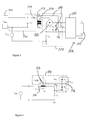
- FIG 3 is presented a preferred embodiment according to the invention, showing a limiter circuit 110 for a connection circuitry making a connection from a power source 100 to a load 102.
- the connection circuitry comprises a common mode choke 104, a first circuit 106 connecting the power source 100 and the common mode choke 104, and a second circuit 108 connecting the common mode choke 104 and the load 102.
- the power source 100 is a mains voltage source
- the load 102 is a lamp 103 together with the control circuitry 105 of the lamp.
- the lamp 103 can be a gas discharge lamp, such as a fluorescent lamp or a high-intensity discharge lamp, or it can be a LED-lamp.
- the control circuitry 105 may comprise the ballast of the lamp, comprising, for example, means for dimming the lamp, or means for preheating the lamp cathodes.
- the load 102 can be any other electrical device that can be connected to a power source 100 using a connection circuitry.
- the limiter circuit 110 comprises a voltage dependent element 112 for decreasing resistivity of said element according to an increase of voltage in said element.
- the voltage dependent element 112 comprises at least two terminals 114, 116, the first terminal 114 being connected to the first circuit 106 and the second terminal 116 being connected to the second circuit 108 bypassing the common mode choke 104.
- the voltage dependent element 112 is a voltage dependent resistor (VDR), which is also known as a varistor. Any other kind of voltage dependent element can be used, such as a silicon controlled rectifier (SCR), also known as a thyristor.
- the connection circuitry also comprises a diode bridge 122 for rectifying alternating mains voltage from the mains voltage source 100 to rectified voltage in the second circuit 108.
- Power source 100 can also be a DC power source, in which case the diode bridge is not needed.
- FIG 4 is presented a simplified schematic of the present invention.
- the voltage dependent resistor 112 is non-conductive until the voltage exceeds the threshold voltage of the voltage dependent resistor.
- the threshold voltage is of the order of 400 V.
- the voltage dependent resistor 112 Once the voltage dependent resistor 112 is conducting, it introduces losses to the circuitry, and thus attenuates the oscillation caused by the surge voltage.
- the voltage dependent resistor prevents high voltages over the Y-capacitor and attenuates the oscillation of the resonance circuit, thus preventing damages and operational failures. After the surge voltage has been attenuated, the voltage dependent element return to non-conductive state.
- voltage dependent resistors 112 typically have large internal capacitance (C S1 in figure 4 ) compared to the internal capacitance (C S2 ) of the common mode choke 104.
- the capacitance of the voltage dependent resistor can be of the order of 100 pF. If the voltage dependent resistor is simply connected in parallel with the common mode choke, during normal operation of the circuitry, interferences intended to be filtered by the common mode choke 104 would be able to bypass the common mode choke via the voltage dependent resistor.
- the limiter circuit also comprises a serial connection of at least two diodes D1, D2 connected to the second circuit 108.
- the second terminal 116 of said voltage dependent resistor 116 is connected in between the at least two diodes D1, D2.
- the serial connection of the at least two diodes D1, D2 is connected to the DC voltage, i.e. to the rectified voltage in the second circuit 108.
- the anode side of the lower serial connected diode D2 is connected to a node between the common mode choke 104 and the Y-capacitor. This way, the serial connected diodes D1, D2 are reverse-biased and are not conductive during normal operation of the circuitry.
- the internal capacitance of the diodes D1, D2 (C SD1 and C SD2 in figure 4 ) is considerably lower than the internal capacitance of the voltage dependent resistor 112.
- the capacitances of the diodes are typically in the range of 2-20 pF, depending on the reverse voltage.
- the capacitance of the serial connection of the at least two diodes needs to be selected to be substantially lower than the capacitance of the voltage dependent resistor in order to decrease the overall capacitance of the limiter circuit 110.
- a low total capacitance of the limiter circuit can be obtained by connecting more than two diodes in series.
- the capacitance of the limiter circuit 110 is of the same order of magnitude as the capacitance of the common mode choke 104, or even lower.
- the capacitance of the limiter circuit 110 is lower than the capacitance of the common mode choke 104, for example, 1% - 30% of the capacitance of the common mode choke.
- the limiter circuit 110 In normal operating conditions, there is preferably no current passing through the limiter circuit 110 according to the invention. As described, the limiter circuit becomes active when the threshold voltage of the voltage dependent element 112 is exceeded.
- FIG 5 is presented with dashed lines alternative locations for the X-capacitor(s) and the Y-capacitor(s) in embodiments according to the invention.
- Y-capacitor can be connected to the ground potential also from the positive rectified voltage, i.e. from the other terminal of the C x2 .
- Figure 5 also shows an alternative location for X-capacitor C x , where it is connected between the common mode choke 104 and the diode bridge 122.
Landscapes
- Rectifiers (AREA)
- Emergency Protection Circuit Devices (AREA)
Abstract
Description
- Many kinds of electrical devices, such as different kinds of lighting devices, need a connection circuitry between a power source and the electrical device.
- A connection circuitry, i.e. a connection device, connects a power source and a load so that electrical energy from the power source is provided in a form suitable to the load using said electrical energy. The load is an electrical device, for example a lighting unit. An important function of the connection circuitry is to prevent different kinds of electrical interferences and disturbances from causing device and/or operational failures.
- There are two main modes of transmission of an electrical surge via cables: a common mode surge and a differential mode surge. A common mode surge produces a voltage between the ground potential and the conductors. The potential difference is the same between each conductor and the ground. A differential mode surge produces a voltage between the two conductors. The potential difference induced by the surge is carried between the two conductors.
- In
figure 1 is presented a prior art connection circuitry between apower source 100, i.e. a voltage source, and aload 102, i.e. an electrical device that uses electrical energy provided by the voltage source. Such a circuitry is known, for example, from "Lighting Control - Technology and Applications" by Robert S. Simpson (Focal Press, 2003), page 220. The connector circuitry comprises a common mode choke LEMI, X-capacitors Cx1 and Cx2, and a Y-capacitor Cy. To some extent, differential mode voltage interferences are filtered by said common mode choke LEMI and X-capacitors Cx1 and Cx2, and common mode interferences by common mode choke LEMI , and the Y-capacitor Cy. - In the prior art arrangement of
figure 1 , thepower source 100 is a mains voltage from an electrical network. Arectifier bridge 122 rectifies alternating voltage provided by the electrical network. Typically, there are requirements concerning surge voltages the connection circuitry must tolerate. For example, in the case of electronic ballasts, standard IEC61000-4-5 requires that the connection circuitry must tolerate a 2 kV common mode surge voltage without damages. This is tested by producing a common mode test surge to the connection circuitry using a surge voltage source. The surge voltage source is denoted by Vsurge in the following description and infigures 2-5 . - In
figure 2 , a simplified schematic of the block diagram offigure 1 during a common mode voltage surge is presented. A surge voltage source Vsurge replaces the mains voltage source. The X-capacitors Cx1 and Cx2 can be considered as short circuits, because their capacitances are about 100-fold compared to the capacitance of the Y-capacitor Cy. The diodes in the rectifier bridge also form a short circuit during a voltage surge. Therefore, the common mode choke and the Y-capacitor form a series resonance circuit as shown infigure 2 . Due to the common mode surge voltage, the voltage of the Y-capacitor may be up to twice the peak value of the surge voltage. A voltage oscillation arises in the resonance frequency of the common mode choke LEMI and the Y-capacitor. In this situation, the common mode choke may saturate, and, therefore, the resonance current or voltage is not sinusoidal. The high, oscillating voltage over the Y-capacitor may cause breakthroughs, damages to sensitive parts of the device, or operational failures. - The object of the invention is to achieve, with reasonable costs, safe operating conditions for an electrical device by preventing high voltage values from arising in a connection circuitry and thus effectively preventing both damages to the electrical device and operational errors in the operation of the electrical device. This is achieved by a limiter circuit for limiting substantially high voltage values from arising in a connection circuitry, the connection circuitry making a connection from a power source to a load, said connection circuitry comprising a common mode choke, a first circuit connecting the power source and the common mode choke, and a second circuit connecting the common mode choke and the load. The limiter circuit comprises a voltage dependent element for decreasing resistivity of said element according to an increase in voltage in said element, said voltage dependent element comprising at least two terminals, the first terminal being connected to the first circuit and the second terminal being connected to the second circuit bypassing the common mode choke, a serial connection of at least two diodes being connected to the second circuit, and the second terminal of the voltage dependent element being connected in between said at least two diodes.
- The object of the invention is also a method for limiting substantially high voltage values from arising in a connection circuitry, the connection circuitry connecting a power source and a load, which connection circuitry comprises a first circuit connecting the power source and a common mode choke, and a second circuit connecting the common mode choke and the load. The voltages in the connection circuitry are limited by a voltage dependent element comprising at least two terminals, where the first terminal is connected to the first circuit and the second terminal is connected to the second circuit bypassing the common mode choke, and the resistivity of the voltage dependent element is arranged to decrease according to an increase in voltage in said element, a serial connection of at least two diodes is connected to the second circuit, and the second terminal of the voltage dependent element is connected in between said at least two diodes.
- According to an embodiment of the invention the voltage dependent element is a voltage dependent resistor.
- In one embodiment of the invention, the power source is a mains voltage source. Alternating mains voltage from the mains voltage source is rectified in the second circuit using a diode bridge.
- In one embodiment of the invention, the serial connection of the at least two diodes is connected to said rectified voltage in the second circuit.
- According to an embodiment of the invention, the capacitance of the serial connection of the at least two diodes is substantially lower than the capacitance of the voltage dependent element in order to decrease the capacitance of the limiter circuit. In a preferred embodiment, the capacitance of the limiter circuit is at most of the same order of magnitude as the capacitance of the common mode choke.
- The invention is based on the utilization of a voltage dependent element in a limiter circuit for a connection circuitry for decreasing resistivity of said element according to an increase of voltage in said element, which limiter circuit bypasses a common mode choke, the first terminal of the voltage dependent element being connected to the power source side in relation to the common mode choke. A serial connection of at least two diodes is connected to the load side in relation to the common mode choke, and the second terminal of the voltage dependent element is connected in between said at least two diodes, which are reverse-biased. The limiter circuit limits substantially high voltage values from arising in the connection circuitry. The benefit of the invention is that it provides a practical and relatively low cost arrangement for preventing high voltage values from arising in a connection circuitry, and thus damages to an electrical device and operational errors due to the high voltage values are avoided.
-
- Figure 1
- presents a block diagram of a prior art connection circuitry.
- Figure 2
- presents a simplified schematic of the block diagram presented in
figure 1 . - Figure 3
- presents a preferred embodiment according to the invention.
- Figure 4
- presents a simplified schematic of the present invention.
- Figure 5
- presents examples of alternative capacitor locations in embodiments according to the invention.
- In order to prevent high, oscillating voltages from arising in the connection circuitry, a limiter circuit comprising damping components is connected to the connection circuitry. In
figure 3 is presented a preferred embodiment according to the invention, showing alimiter circuit 110 for a connection circuitry making a connection from apower source 100 to aload 102. The connection circuitry comprises a common mode choke 104, a first circuit 106 connecting thepower source 100 and the common mode choke 104, and a second circuit 108 connecting the common mode choke 104 and theload 102. In the embodiment offigure 3 , thepower source 100 is a mains voltage source, and theload 102 is alamp 103 together with thecontrol circuitry 105 of the lamp. Thelamp 103 can be a gas discharge lamp, such as a fluorescent lamp or a high-intensity discharge lamp, or it can be a LED-lamp. Thecontrol circuitry 105 may comprise the ballast of the lamp, comprising, for example, means for dimming the lamp, or means for preheating the lamp cathodes. However, theload 102 can be any other electrical device that can be connected to apower source 100 using a connection circuitry. Thelimiter circuit 110 comprises a voltagedependent element 112 for decreasing resistivity of said element according to an increase of voltage in said element. The voltagedependent element 112 comprises at least twoterminals 114, 116, thefirst terminal 114 being connected to the first circuit 106 and the second terminal 116 being connected to the second circuit 108 bypassing the common mode choke 104. In this preferred embodiment, the voltagedependent element 112 is a voltage dependent resistor (VDR), which is also known as a varistor. Any other kind of voltage dependent element can be used, such as a silicon controlled rectifier (SCR), also known as a thyristor. The connection circuitry also comprises adiode bridge 122 for rectifying alternating mains voltage from themains voltage source 100 to rectified voltage in the second circuit 108.Power source 100 can also be a DC power source, in which case the diode bridge is not needed. - In
figure 4 is presented a simplified schematic of the present invention.
The voltagedependent resistor 112 is non-conductive until the voltage exceeds the threshold voltage of the voltage dependent resistor. For a typical voltage dependent resistor to be used, the threshold voltage is of the order of 400 V. Once the voltagedependent resistor 112 is conducting, it introduces losses to the circuitry, and thus attenuates the oscillation caused by the surge voltage. The voltage dependent resistor prevents high voltages over the Y-capacitor and attenuates the oscillation of the resonance circuit, thus preventing damages and operational failures. After the surge voltage has been attenuated, the voltage dependent element return to non-conductive state. - However, voltage
dependent resistors 112 typically have large internal capacitance (CS1 infigure 4 ) compared to the internal capacitance (CS2) of the common mode choke 104. The capacitance of the voltage dependent resistor can be of the order of 100 pF. If the voltage dependent resistor is simply connected in parallel with the common mode choke, during normal operation of the circuitry, interferences intended to be filtered by the common mode choke 104 would be able to bypass the common mode choke via the voltage dependent resistor. - Therefore, according to the present invention, the limiter circuit also comprises a serial connection of at least two diodes D1, D2 connected to the second circuit 108. The second terminal 116 of said voltage dependent resistor 116 is connected in between the at least two diodes D1, D2. As presented in
figures 3 and 4 , the serial connection of the at least two diodes D1, D2 is connected to the DC voltage, i.e. to the rectified voltage in the second circuit 108. The anode side of the lower serial connected diode D2 is connected to a node between the common mode choke 104 and the Y-capacitor. This way, the serial connected diodes D1, D2 are reverse-biased and are not conductive during normal operation of the circuitry. - The internal capacitance of the diodes D1, D2 (CSD1 and CSD2 in
figure 4 ) is considerably lower than the internal capacitance of the voltagedependent resistor 112. The capacitances of the diodes are typically in the range of 2-20 pF, depending on the reverse voltage. The capacitance of the serial connection of the at least two diodes needs to be selected to be substantially lower than the capacitance of the voltage dependent resistor in order to decrease the overall capacitance of thelimiter circuit 110. The total capacitance of the limiter circuit is calculated according to the following equation
- , where Ctot is the total capacitance of the limiter circuit 11
- CSD1 is the internal capacitance of the first diode D1,
- CSD2 is the internal capacitance of the second diode D2, and
- CS1 is the internal capacitance of the voltage
dependent resistor 112. - If diodes with sufficiently low capacitance values are not available, a low total capacitance of the limiter circuit can be obtained by connecting more than two diodes in series.
- When the overall capacitance of the
limiter circuit 110 is low, interference attenuation characteristics of the common mode choke 104 are not compromised during normal operation of the circuitry. Advantageously, the capacitance of thelimiter circuit 110 is of the same order of magnitude as the capacitance of the common mode choke 104, or even lower. Preferably the capacitance of thelimiter circuit 110 is lower than the capacitance of the common mode choke 104, for example, 1% - 30% of the capacitance of the common mode choke. - In normal operating conditions, there is preferably no current passing through the
limiter circuit 110 according to the invention. As described, the limiter circuit becomes active when the threshold voltage of the voltagedependent element 112 is exceeded. - In
figure 5 is presented with dashed lines alternative locations for the X-capacitor(s) and the Y-capacitor(s) in embodiments according to the invention. Y-capacitor can be connected to the ground potential also from the positive rectified voltage, i.e. from the other terminal of the Cx2. There can also be two Y-capacitors, one connected from the negative rectified voltage to the ground potential, and the other one connected from the positive rectified voltage to the ground potential.Figure 5 also shows an alternative location for X-capacitor Cx, where it is connected between the common mode choke 104 and thediode bridge 122. - Although the invention has been presented in reference to the attached figures and specification, the invention is by no means limited to those, as the invention is subject to variations within the scope allowed for by the claims.
Claims (14)
- A limiter circuit (110) for limiting substantially high voltage values from arising in a connection circuitry, the connection circuitry making a connection from a power source (100) to a load (102), said connection circuitry comprising a common mode choke (104), a first circuit (106) connecting the power source (100) and the common mode choke (104), and a second circuit (108) connecting the common mode choke (104) and the load (102), characterized in that the limiter circuit (110) comprises a voltage dependent element (112) for decreasing resistivity of said element (112) according to an increase in voltage in said element (112), said voltage dependent element comprising at least two terminals (114, 116), the first terminal (114) being connected to the first circuit (106) and the second terminal (116) being connected to the second circuit (108) bypassing the common mode choke (104), a serial connection of at least two diodes (D1, D2) being connected to the second circuit (108), and the second terminal (116) of the voltage dependent element (112) being connected in between said at least two diodes (D1, D2).
- A limiter circuit (110) for a connection circuitry in accordance with claim 1, characterized in that the voltage dependent element (112) between the first circuit (106) and the second circuit (108) comprises a voltage dependent resistor (112).
- A limiter circuit (110) for a connection circuitry in accordance with claim 1, characterized in that the power source (100) is a mains voltage source (100).
- A limiter circuit (110) for a connection circuitry in accordance with claim 3, characterized in that the connection circuitry comprises a diode bridge (122) for rectifying alternating mains voltage from the mains voltage source (100) to rectified voltage in the second circuit (108).
- A limiter circuit (110) for a connection circuitry in accordance with claim 4, characterized by the serial connection of the at least two diodes (D1, D2) being connected to said rectified voltage in the second circuit (108).
- A limiter circuit (110) for a connection circuitry in accordance with claim 1, characterized in that the capacitance of the serial connection of the at least two diodes (D1, D2) is substantially lower than the capacitance of the voltage dependent element (112) in order to decrease the capacitance of the limiter circuit (110).
- A limiter circuit (110) for a connection circuitry in accordance with claim 6, characterized in that the capacitance of the limiter circuit (110) is at most of the same order of magnitude as the capacitance of the common mode choke (104).
- A method for limiting substantially high voltage values from arising in a connection circuitry, the connection circuitry connecting a power source (100) and a load (102), which connection circuitry comprises a first circuit (106) connecting the power source (100) and a common mode choke (104), and a second circuit (108) connecting the common mode choke (104) and the load (102), characterized in that the voltages in the connection circuitry are limited by a voltage dependent element (112) comprising at least two terminals (114, 116), where the first terminal (114) is connected to the first circuit (106) and the second terminal (116) is connected to the second circuit (108) bypassing the common mode choke (104), and the resistivity of the voltage dependent element (112) is arranged to decrease according to an increase in voltage in said element (112), a serial connection of at least two diodes (D1, D2) is connected to the second circuit (108), and the second terminal (116) of the voltage dependent element (112) is connected in between said at least two diodes (D1, D2).
- A method for limiting substantially high voltage values from arising in a connection circuitry in accordance with claim 8, characterized in that as the voltage dependent element (112) between the first circuit (106) and the second circuit (108) is utilized a voltage dependent resistor (112).
- A method for limiting substantially high voltage values from arising in a connection circuitry in accordance with claim 8, characterized in that the power source (100) is a mains voltage source (100).
- A method for limiting substantially high voltage values from arising in a connection circuitry in accordance with claim 10, characterized in that alternating mains voltage from the mains voltage source (100) is rectified in the second circuit (108).
- A method for limiting substantially high voltage values from arising in a connection circuitry in accordance with claim 11, characterized in that the serial connection of the at least two diodes (D1, D2) is connected to said rectified voltage in the second circuit (108).
- A method for limiting substantially high voltage values from arising in a connection circuitry in accordance with claim 8, characterized in that the capacitance of the serial connection of the at least two diodes (D1, D2) is arranged to be substantially lower than the capacitance of the voltage dependent element (112) in order to decrease the capacitance of the limiter circuit (110).
- A method limiting substantially high voltage values from arising in a connection circuitry in accordance with claim 13, characterized in that the capacitance of the limiter circuit (110) is arranged to be at most of the same order of magnitude as the capacitance of the common mode choke (104).
Priority Applications (1)
| Application Number | Priority Date | Filing Date | Title |
|---|---|---|---|
| EP10189055.6A EP2448077B1 (en) | 2010-10-27 | 2010-10-27 | A limiter circuit for limiting voltages |
Applications Claiming Priority (1)
| Application Number | Priority Date | Filing Date | Title |
|---|---|---|---|
| EP10189055.6A EP2448077B1 (en) | 2010-10-27 | 2010-10-27 | A limiter circuit for limiting voltages |
Publications (2)
| Publication Number | Publication Date |
|---|---|
| EP2448077A1 true EP2448077A1 (en) | 2012-05-02 |
| EP2448077B1 EP2448077B1 (en) | 2016-06-22 |
Family
ID=43706421
Family Applications (1)
| Application Number | Title | Priority Date | Filing Date |
|---|---|---|---|
| EP10189055.6A Active EP2448077B1 (en) | 2010-10-27 | 2010-10-27 | A limiter circuit for limiting voltages |
Country Status (1)
| Country | Link |
|---|---|
| EP (1) | EP2448077B1 (en) |
Citations (3)
| Publication number | Priority date | Publication date | Assignee | Title |
|---|---|---|---|---|
| US5313358A (en) * | 1991-12-13 | 1994-05-17 | Premier Power, Inc. | Multiphase common mode transient suppressor |
| JPH10191557A (en) * | 1996-12-25 | 1998-07-21 | Canon Inc | Power line filter device |
| US20070081289A1 (en) * | 2005-10-11 | 2007-04-12 | Jason Pierce | System for EMI filter surge voltage clamping |
-
2010
- 2010-10-27 EP EP10189055.6A patent/EP2448077B1/en active Active
Patent Citations (3)
| Publication number | Priority date | Publication date | Assignee | Title |
|---|---|---|---|---|
| US5313358A (en) * | 1991-12-13 | 1994-05-17 | Premier Power, Inc. | Multiphase common mode transient suppressor |
| JPH10191557A (en) * | 1996-12-25 | 1998-07-21 | Canon Inc | Power line filter device |
| US20070081289A1 (en) * | 2005-10-11 | 2007-04-12 | Jason Pierce | System for EMI filter surge voltage clamping |
Also Published As
| Publication number | Publication date |
|---|---|
| EP2448077B1 (en) | 2016-06-22 |
Similar Documents
| Publication | Publication Date | Title |
|---|---|---|
| CN213275752U (en) | Connection system for voltage absence detector | |
| US9735725B2 (en) | Methods and systems for transient voltage protection | |
| US8520355B2 (en) | Methods and systems for transient voltage protection | |
| US10219334B2 (en) | Circuit arrangement for operating semiconductor light sources | |
| US20120014144A1 (en) | Power supplying apparatus | |
| CN110676827B (en) | Power electronic device | |
| JP4983677B2 (en) | Surge absorption circuit | |
| WO2017114114A1 (en) | Led device protection circuit and method thereof | |
| CN109494702A (en) | A kind of capacitance protection circuit and power protecting circuit | |
| CN109245508B (en) | Electronic device | |
| EP2966745B1 (en) | Transient voltage protection for bridge rectifier | |
| EP1782516A2 (en) | Resistor dropper power supply with surge protection | |
| JP6317539B2 (en) | Voltage change device for electric meters | |
| CN108767829A (en) | A kind of surging protection circuit | |
| US8129982B2 (en) | Voltage sensing circuits and methods for inverters | |
| US9379533B1 (en) | Input surge protection circuit and method for an LED load | |
| EP2448077B1 (en) | A limiter circuit for limiting voltages | |
| US7643260B2 (en) | System for EMI filter surge voltage clamping | |
| JP2012095446A (en) | Power supply unit and withstand voltage test method therefor | |
| NZ243218A (en) | Power supply for fluorescent lamp has capacitor bank connected between rectifier input and output to reduce harmonic distortion of ac supply current | |
| CN209748190U (en) | Protection circuit and electronic equipment | |
| CN208638022U (en) | A kind of surging protection circuit | |
| CN220042989U (en) | Surge protection circuit and switching power supply | |
| US20260136441A1 (en) | High-compatibility multifunctional lighting device | |
| JP7087439B2 (en) | Lighting equipment, lighting fixtures and lighting systems |
Legal Events
| Date | Code | Title | Description |
|---|---|---|---|
| PUAI | Public reference made under article 153(3) epc to a published international application that has entered the european phase |
Free format text: ORIGINAL CODE: 0009012 |
|
| AK | Designated contracting states |
Kind code of ref document: A1 Designated state(s): AL AT BE BG CH CY CZ DE DK EE ES FI FR GB GR HR HU IE IS IT LI LT LU LV MC MK MT NL NO PL PT RO RS SE SI SK SM TR |
|
| AX | Request for extension of the european patent |
Extension state: BA ME |
|
| 17P | Request for examination filed |
Effective date: 20121102 |
|
| 17Q | First examination report despatched |
Effective date: 20151014 |
|
| GRAP | Despatch of communication of intention to grant a patent |
Free format text: ORIGINAL CODE: EPIDOSNIGR1 |
|
| RIC1 | Information provided on ipc code assigned before grant |
Ipc: H05B 41/285 20060101ALI20160229BHEP Ipc: H02H 9/04 20060101ALI20160229BHEP Ipc: H02H 9/00 20060101AFI20160229BHEP |
|
| INTG | Intention to grant announced |
Effective date: 20160329 |
|
| GRAS | Grant fee paid |
Free format text: ORIGINAL CODE: EPIDOSNIGR3 |
|
| GRAA | (expected) grant |
Free format text: ORIGINAL CODE: 0009210 |
|
| AK | Designated contracting states |
Kind code of ref document: B1 Designated state(s): AL AT BE BG CH CY CZ DE DK EE ES FI FR GB GR HR HU IE IS IT LI LT LU LV MC MK MT NL NO PL PT RO RS SE SI SK SM TR |
|
| RAP1 | Party data changed (applicant data changed or rights of an application transferred) |
Owner name: HELVAR OY AB |
|
| REG | Reference to a national code |
Ref country code: GB Ref legal event code: FG4D |
|
| RIN1 | Information on inventor provided before grant (corrected) |
Inventor name: PERKIOE, TUOMAS Inventor name: VIHINEN, HANNU |
|
| REG | Reference to a national code |
Ref country code: CH Ref legal event code: EP |
|
| REG | Reference to a national code |
Ref country code: IE Ref legal event code: FG4D |
|
| REG | Reference to a national code |
Ref country code: AT Ref legal event code: REF Ref document number: 808162 Country of ref document: AT Kind code of ref document: T Effective date: 20160715 |
|
| REG | Reference to a national code |
Ref country code: DE Ref legal event code: R096 Ref document number: 602010034138 Country of ref document: DE |
|
| REG | Reference to a national code |
Ref country code: LT Ref legal event code: MG4D |
|
| REG | Reference to a national code |
Ref country code: NL Ref legal event code: MP Effective date: 20160622 |
|
| PG25 | Lapsed in a contracting state [announced via postgrant information from national office to epo] |
Ref country code: NO Free format text: LAPSE BECAUSE OF FAILURE TO SUBMIT A TRANSLATION OF THE DESCRIPTION OR TO PAY THE FEE WITHIN THE PRESCRIBED TIME-LIMIT Effective date: 20160922 Ref country code: LT Free format text: LAPSE BECAUSE OF FAILURE TO SUBMIT A TRANSLATION OF THE DESCRIPTION OR TO PAY THE FEE WITHIN THE PRESCRIBED TIME-LIMIT Effective date: 20160622 Ref country code: FI Free format text: LAPSE BECAUSE OF FAILURE TO SUBMIT A TRANSLATION OF THE DESCRIPTION OR TO PAY THE FEE WITHIN THE PRESCRIBED TIME-LIMIT Effective date: 20160622 |
|
| REG | Reference to a national code |
Ref country code: AT Ref legal event code: MK05 Ref document number: 808162 Country of ref document: AT Kind code of ref document: T Effective date: 20160622 |
|
| PG25 | Lapsed in a contracting state [announced via postgrant information from national office to epo] |
Ref country code: RS Free format text: LAPSE BECAUSE OF FAILURE TO SUBMIT A TRANSLATION OF THE DESCRIPTION OR TO PAY THE FEE WITHIN THE PRESCRIBED TIME-LIMIT Effective date: 20160622 Ref country code: GR Free format text: LAPSE BECAUSE OF FAILURE TO SUBMIT A TRANSLATION OF THE DESCRIPTION OR TO PAY THE FEE WITHIN THE PRESCRIBED TIME-LIMIT Effective date: 20160923 Ref country code: LV Free format text: LAPSE BECAUSE OF FAILURE TO SUBMIT A TRANSLATION OF THE DESCRIPTION OR TO PAY THE FEE WITHIN THE PRESCRIBED TIME-LIMIT Effective date: 20160622 Ref country code: SE Free format text: LAPSE BECAUSE OF FAILURE TO SUBMIT A TRANSLATION OF THE DESCRIPTION OR TO PAY THE FEE WITHIN THE PRESCRIBED TIME-LIMIT Effective date: 20160622 Ref country code: HR Free format text: LAPSE BECAUSE OF FAILURE TO SUBMIT A TRANSLATION OF THE DESCRIPTION OR TO PAY THE FEE WITHIN THE PRESCRIBED TIME-LIMIT Effective date: 20160622 Ref country code: NL Free format text: LAPSE BECAUSE OF FAILURE TO SUBMIT A TRANSLATION OF THE DESCRIPTION OR TO PAY THE FEE WITHIN THE PRESCRIBED TIME-LIMIT Effective date: 20160622 |
|
| PG25 | Lapsed in a contracting state [announced via postgrant information from national office to epo] |
Ref country code: SK Free format text: LAPSE BECAUSE OF FAILURE TO SUBMIT A TRANSLATION OF THE DESCRIPTION OR TO PAY THE FEE WITHIN THE PRESCRIBED TIME-LIMIT Effective date: 20160622 Ref country code: IS Free format text: LAPSE BECAUSE OF FAILURE TO SUBMIT A TRANSLATION OF THE DESCRIPTION OR TO PAY THE FEE WITHIN THE PRESCRIBED TIME-LIMIT Effective date: 20161022 Ref country code: RO Free format text: LAPSE BECAUSE OF FAILURE TO SUBMIT A TRANSLATION OF THE DESCRIPTION OR TO PAY THE FEE WITHIN THE PRESCRIBED TIME-LIMIT Effective date: 20160622 Ref country code: IT Free format text: LAPSE BECAUSE OF FAILURE TO SUBMIT A TRANSLATION OF THE DESCRIPTION OR TO PAY THE FEE WITHIN THE PRESCRIBED TIME-LIMIT Effective date: 20160622 Ref country code: CZ Free format text: LAPSE BECAUSE OF FAILURE TO SUBMIT A TRANSLATION OF THE DESCRIPTION OR TO PAY THE FEE WITHIN THE PRESCRIBED TIME-LIMIT Effective date: 20160622 Ref country code: EE Free format text: LAPSE BECAUSE OF FAILURE TO SUBMIT A TRANSLATION OF THE DESCRIPTION OR TO PAY THE FEE WITHIN THE PRESCRIBED TIME-LIMIT Effective date: 20160622 |
|
| PG25 | Lapsed in a contracting state [announced via postgrant information from national office to epo] |
Ref country code: PL Free format text: LAPSE BECAUSE OF FAILURE TO SUBMIT A TRANSLATION OF THE DESCRIPTION OR TO PAY THE FEE WITHIN THE PRESCRIBED TIME-LIMIT Effective date: 20160622 Ref country code: ES Free format text: LAPSE BECAUSE OF FAILURE TO SUBMIT A TRANSLATION OF THE DESCRIPTION OR TO PAY THE FEE WITHIN THE PRESCRIBED TIME-LIMIT Effective date: 20160622 Ref country code: BE Free format text: LAPSE BECAUSE OF NON-PAYMENT OF DUE FEES Effective date: 20160622 Ref country code: PT Free format text: LAPSE BECAUSE OF FAILURE TO SUBMIT A TRANSLATION OF THE DESCRIPTION OR TO PAY THE FEE WITHIN THE PRESCRIBED TIME-LIMIT Effective date: 20161024 Ref country code: SM Free format text: LAPSE BECAUSE OF FAILURE TO SUBMIT A TRANSLATION OF THE DESCRIPTION OR TO PAY THE FEE WITHIN THE PRESCRIBED TIME-LIMIT Effective date: 20160622 Ref country code: AT Free format text: LAPSE BECAUSE OF FAILURE TO SUBMIT A TRANSLATION OF THE DESCRIPTION OR TO PAY THE FEE WITHIN THE PRESCRIBED TIME-LIMIT Effective date: 20160622 |
|
| REG | Reference to a national code |
Ref country code: DE Ref legal event code: R097 Ref document number: 602010034138 Country of ref document: DE |
|
| PLBE | No opposition filed within time limit |
Free format text: ORIGINAL CODE: 0009261 |
|
| STAA | Information on the status of an ep patent application or granted ep patent |
Free format text: STATUS: NO OPPOSITION FILED WITHIN TIME LIMIT |
|
| 26N | No opposition filed |
Effective date: 20170323 |
|
| PG25 | Lapsed in a contracting state [announced via postgrant information from national office to epo] |
Ref country code: DK Free format text: LAPSE BECAUSE OF FAILURE TO SUBMIT A TRANSLATION OF THE DESCRIPTION OR TO PAY THE FEE WITHIN THE PRESCRIBED TIME-LIMIT Effective date: 20160622 |
|
| REG | Reference to a national code |
Ref country code: CH Ref legal event code: PL |
|
| GBPC | Gb: european patent ceased through non-payment of renewal fee |
Effective date: 20161027 |
|
| REG | Reference to a national code |
Ref country code: IE Ref legal event code: MM4A |
|
| REG | Reference to a national code |
Ref country code: FR Ref legal event code: ST Effective date: 20170630 |
|
| PG25 | Lapsed in a contracting state [announced via postgrant information from national office to epo] |
Ref country code: CH Free format text: LAPSE BECAUSE OF NON-PAYMENT OF DUE FEES Effective date: 20161031 Ref country code: GB Free format text: LAPSE BECAUSE OF NON-PAYMENT OF DUE FEES Effective date: 20161027 Ref country code: LI Free format text: LAPSE BECAUSE OF NON-PAYMENT OF DUE FEES Effective date: 20161031 Ref country code: FR Free format text: LAPSE BECAUSE OF NON-PAYMENT OF DUE FEES Effective date: 20161102 |
|
| PG25 | Lapsed in a contracting state [announced via postgrant information from national office to epo] |
Ref country code: LU Free format text: LAPSE BECAUSE OF NON-PAYMENT OF DUE FEES Effective date: 20161027 Ref country code: SI Free format text: LAPSE BECAUSE OF FAILURE TO SUBMIT A TRANSLATION OF THE DESCRIPTION OR TO PAY THE FEE WITHIN THE PRESCRIBED TIME-LIMIT Effective date: 20160622 |
|
| PG25 | Lapsed in a contracting state [announced via postgrant information from national office to epo] |
Ref country code: IE Free format text: LAPSE BECAUSE OF NON-PAYMENT OF DUE FEES Effective date: 20161027 |
|
| PG25 | Lapsed in a contracting state [announced via postgrant information from national office to epo] |
Ref country code: CY Free format text: LAPSE BECAUSE OF FAILURE TO SUBMIT A TRANSLATION OF THE DESCRIPTION OR TO PAY THE FEE WITHIN THE PRESCRIBED TIME-LIMIT Effective date: 20160622 Ref country code: HU Free format text: LAPSE BECAUSE OF FAILURE TO SUBMIT A TRANSLATION OF THE DESCRIPTION OR TO PAY THE FEE WITHIN THE PRESCRIBED TIME-LIMIT; INVALID AB INITIO Effective date: 20101027 |
|
| PG25 | Lapsed in a contracting state [announced via postgrant information from national office to epo] |
Ref country code: TR Free format text: LAPSE BECAUSE OF FAILURE TO SUBMIT A TRANSLATION OF THE DESCRIPTION OR TO PAY THE FEE WITHIN THE PRESCRIBED TIME-LIMIT Effective date: 20160622 Ref country code: MT Free format text: LAPSE BECAUSE OF NON-PAYMENT OF DUE FEES Effective date: 20161031 Ref country code: MK Free format text: LAPSE BECAUSE OF FAILURE TO SUBMIT A TRANSLATION OF THE DESCRIPTION OR TO PAY THE FEE WITHIN THE PRESCRIBED TIME-LIMIT Effective date: 20160622 Ref country code: MC Free format text: LAPSE BECAUSE OF FAILURE TO SUBMIT A TRANSLATION OF THE DESCRIPTION OR TO PAY THE FEE WITHIN THE PRESCRIBED TIME-LIMIT Effective date: 20160622 |
|
| PG25 | Lapsed in a contracting state [announced via postgrant information from national office to epo] |
Ref country code: BG Free format text: LAPSE BECAUSE OF FAILURE TO SUBMIT A TRANSLATION OF THE DESCRIPTION OR TO PAY THE FEE WITHIN THE PRESCRIBED TIME-LIMIT Effective date: 20160622 |
|
| PG25 | Lapsed in a contracting state [announced via postgrant information from national office to epo] |
Ref country code: AL Free format text: LAPSE BECAUSE OF FAILURE TO SUBMIT A TRANSLATION OF THE DESCRIPTION OR TO PAY THE FEE WITHIN THE PRESCRIBED TIME-LIMIT Effective date: 20160622 |
|
| PGFP | Annual fee paid to national office [announced via postgrant information from national office to epo] |
Ref country code: DE Payment date: 20251029 Year of fee payment: 16 |
|
| REG | Reference to a national code |
Ref country code: DE Ref legal event code: R081 Ref document number: 602010034138 Country of ref document: DE Owner name: HELVAR COMPONENTS OY AB, FI Free format text: FORMER OWNER: HELVAR OY AB, ESPOO, FI Ref country code: DE Ref legal event code: R082 Ref document number: 602010034138 Country of ref document: DE Representative=s name: DENNEMEYER & ASSOCIATES RECHTSANWALTSGESELLSCH, DE |