EP2445104A2 - Very high efficiency flexible travelling wave amplifier - Google Patents
Very high efficiency flexible travelling wave amplifier Download PDFInfo
- Publication number
- EP2445104A2 EP2445104A2 EP11186209A EP11186209A EP2445104A2 EP 2445104 A2 EP2445104 A2 EP 2445104A2 EP 11186209 A EP11186209 A EP 11186209A EP 11186209 A EP11186209 A EP 11186209A EP 2445104 A2 EP2445104 A2 EP 2445104A2
- Authority
- EP
- European Patent Office
- Prior art keywords
- helix
- travelling wave
- voltage
- wave tube
- cathode
- Prior art date
- Legal status (The legal status is an assumption and is not a legal conclusion. Google has not performed a legal analysis and makes no representation as to the accuracy of the status listed.)
- Granted
Links
- 230000010287 polarization Effects 0.000 claims abstract description 4
- 238000010894 electron beam technology Methods 0.000 description 10
- 230000008901 benefit Effects 0.000 description 9
- 230000033228 biological regulation Effects 0.000 description 9
- 238000010586 diagram Methods 0.000 description 8
- 239000003990 capacitor Substances 0.000 description 4
- 238000004891 communication Methods 0.000 description 3
- 238000000034 method Methods 0.000 description 3
- 238000007493 shaping process Methods 0.000 description 3
- 238000012546 transfer Methods 0.000 description 3
- 230000006978 adaptation Effects 0.000 description 2
- 238000005516 engineering process Methods 0.000 description 2
- 238000001914 filtration Methods 0.000 description 2
- 238000005259 measurement Methods 0.000 description 2
- 206010063344 microscopic polyangiitis Diseases 0.000 description 2
- 239000007787 solid Substances 0.000 description 2
- 238000004804 winding Methods 0.000 description 2
- 230000003321 amplification Effects 0.000 description 1
- 230000005540 biological transmission Effects 0.000 description 1
- 230000015556 catabolic process Effects 0.000 description 1
- 230000003750 conditioning effect Effects 0.000 description 1
- 238000012937 correction Methods 0.000 description 1
- 238000006731 degradation reaction Methods 0.000 description 1
- 230000001419 dependent effect Effects 0.000 description 1
- 238000013461 design Methods 0.000 description 1
- 238000011161 development Methods 0.000 description 1
- 230000000694 effects Effects 0.000 description 1
- 230000005672 electromagnetic field Effects 0.000 description 1
- 239000012212 insulator Substances 0.000 description 1
- 230000010354 integration Effects 0.000 description 1
- 230000003993 interaction Effects 0.000 description 1
- 238000002955 isolation Methods 0.000 description 1
- 238000004519 manufacturing process Methods 0.000 description 1
- 238000003199 nucleic acid amplification method Methods 0.000 description 1
- 238000005457 optimization Methods 0.000 description 1
- 238000004064 recycling Methods 0.000 description 1
- 239000011347 resin Substances 0.000 description 1
- 229920005989 resin Polymers 0.000 description 1
- 238000012360 testing method Methods 0.000 description 1
- 230000001052 transient effect Effects 0.000 description 1
Images


Classifications
-
- H—ELECTRICITY
- H03—ELECTRONIC CIRCUITRY
- H03F—AMPLIFIERS
- H03F3/00—Amplifiers with only discharge tubes or only semiconductor devices as amplifying elements
- H03F3/54—Amplifiers using transit-time effect in tubes or semiconductor devices
- H03F3/58—Amplifiers using transit-time effect in tubes or semiconductor devices using travelling-wave tubes
Definitions
- the current invention relates to a very high efficiency flexible travelling wave amplifier. It notably applies to telecommunication satellites.
- Telecommunication satellites usually comprise a platform and a payload, the latter being comprising all equipments, notably all devices intended for generating and transmitting high power radiofrequency signals - hereinafter referred to as RF signals - toward the ground.
- RF signals radiofrequency signals
- Different known techniques are resorted to for transmitting high power RF signals.
- a first technique is based on the solid state technology, and involves Solid State Power Amplifiers, usually referred to as SSPAs.
- SSPAs notably have the drawback of not being in a position to manage usually requested levels of RF power.
- TWTAs notably comprise a Travelling Wave Tube, hereinafter referred to as TWT.
- TWTAs are particularly efficient devices for high power RF transmission channels, and allow for managing very high levels of transmitted RF power.
- TWTA relies on a tube-based technology which requests a very precise tuning, not only on the manufacturing level, but also as regard to the accuracy of electrical interfaces.
- a TWT is described in much detail below in reference to Figure 1 , and basically comprises an RF input and an RF output, a helix, and electrodes comprising a cathode emitting electrons forming an electron beam, an anode, usually referred to as "Anode Zero” or “Anode 0", focussing the electron beam, and a plurality of collectors.
- each produced TWTA is unique, and optimized for the purpose of a unique application, in terms of transmitted frequency, level of transmitted power and efficiency.
- a TWTA and its associated control equipment have to keep operating the same way all through a satellite's assembly, integration and testing, and the in-flight mission of the satellite they are set in. That is: once the telecommunication satellite has been assembled, these equipments shall be operated under the specific conditions they have been designed for.
- the efficiency performance of TWTAs is frequency-dependent. Therefore, in parallel, a satellite intended for transmitting through a plurality of channels, shall be containing as many TWTAs, with related consequences in terms of cost, weight and bulk.
- one TWTA being usually destined to transmit through one given channel over a typical mission duration of more than 15 years makes the payload design and the TWTA procurement very constraining and induces severe constraints in terms of risk management.
- Wide-band TWTAs are known in the prior art, but existing devices typically suffer an efficiency degradation of about 2 percents compared to analogue TWTAs optimized in a narrower RF band.
- One aim of the current invention is to palliate at least the above-mentioned drawbacks, by proposing a TWTA presenting an efficiency similar to that of known tuned narrow band TWTAs, while being able to be operated over a large variety of frequencies, as a wide band TWTA.
- TWTA offers the ability of being easily controlled not only on ground, but also during in-flight operations over a satellite mission.
- TWTA uses control electronics that can be adaptable for any existing high voltage electronic circuitry.
- One further advantage of the current invention is that it alleviates resorting to redundancy of onboard TWTs for given applications, as all TWTs controlled within TWTAs following embodiments of the current invention, can be operated over a wide band.
- One further advantage of the current invention is that it allows mission profile adaptation throughout the satellite payload life, without affecting the global payload efficiency.
- One further advantage of the current invention is that it offers a phase flexibility affording the opportunity to replace phase shifter dedicated hardware in certain applications.
- the current invention proposes a travelling wave tube amplifier comprising at least a travelling wave tube comprising a cathode, a helix, an RF input, an RF output, and a plurality of collectors C i ; an electronic power conditioner providing power supply and electrode polarization to said travelling wave tube; the travelling wave tube amplifier being characterized in that said electronic power conditioner comprises flexibility control means allowing to adjust, via control commands, the helix to cathode voltage, so as to allow adjusting the TWT operating frequency within a determined range with an optimal efficiency.
- the flexibility control means can also be configured to adjust the collector C i voltages, the ratio between the helix to cathode voltage and collector C i voltages remaining constant.
- control commands can be sent through a databus.
- the electronic power conditioner can comprise primary control means comprising a power cell driving a high voltage generation and control means comprising a multistage high voltage transformer whose primary side is controlled by said power cell and generating the high voltages requested by said at least one collector, cathode and helix, said flexibility control means comprising means for adjusting a voltage reference driving a voltage control loop, said voltage control loop being driving the power cell through pulse width modulation.
- the high voltage generation and control means can comprise a regulator attached to the secondary side of said multistage high voltage transformer and supplying a helix to cathode voltage, being adjusted to a helix to cathode voltage reference comprised in said flexibility control means.
- the flexibility control means can further comprise a decoder issuing signal control words from said control commands, and said helix to cathode voltage reference can comprise a first digital-to-analog converter converting binary output words generated by a decoder based upon input binary words sent via said databus.
- said means for adjusting the voltage reference can comprise a second digital-to-analog converter converting binary output words generated by the decoder based upon input binary words sent via said databus.
- said decoder can generate n-bit output words towards the helix to cathode voltage reference, and m-bit output words, m being lower than n, towards the means for adjusting the voltage reference, based upon n-bit input words received from the databus.
- the number m of bits of the output words towards the means for adjusting the voltage reference can be chosen so as to allow adjusting the RF signal phase.
- the high voltage generation and control means can be implemented within a high voltage generation and control module comprising at its input the secondary side of the high voltage transformer also connected to a helix voltage accuracy controller formed by a bipolar transistor driven by the regulator, and whose emitter is attached to the ground through a dissipating element.
- FIG. 1 presents a perspective view depicting a typical TWT known in the prior art.
- a TWT is one of the key elements comprised in a TWTA.
- a TWT 10 is basically an elongated vacuum tube comprising a radiofrequency input 12 and a radiofrequency output 14, a cathode 15 forming an electron gun generating an electron beam 17 focused and adjusted by an Anode Zero 13 passing through a helix 18 up to a plurality of collectors 19.
- the cathode 15 is heated and emits electrons at one of its ends.
- a magnetic field is generated substantially around the helix 18 so as to contain the electrons as the focused electron beam 17.
- the electron beam passes through along the middle axis of the helix 18.
- the helix 18 is extending from the RF input 12 to the RF output 14.
- the electron beam 17 is finally striking the collectors 19.
- the RF signal travels along the helix 18 at a speed that is close to that of the electron beam 17.
- the amplification effect is due to the interaction between the electromagnetic field induced by the RF signal in the helix 18, and the electron beam 17 through a quantum phenomenon.
- a plurality of collectors 19, typically: four or five, may be employed.
- a TWTA usually comprises a TWT, associated with an additional Electronic Power Conditioner, hereinafter referred to as EPC, whose purpose is to supply the TWT with requested electrical operational conditions.
- the EPC is usually a DC-DC converter supplied in energy through a bus, and generating the voltage supply levels requested on each of the electrodes comprised in the TWT, with an accuracy level allowing to ensure the TWT performances, that is: the efficiency and the stability of the power transfer.
- the high voltage between helix 18 and cathode 15 shall be enough accurate, as it is determining the TWT performance.
- the helix - cathode voltage accuracies on the order of 1 Volt are required, for voltages ranking up to several kilovolts; for instance, the required voltages between the helix and the cathode for applications within the Ku band is typically on the order of 6 kilovolts to 7.5 kilovolts. Control of said voltage levels is managed by the EPC.
- Anode Zero 13 allows controlling the electron beam 17 generated by the cathode 15.
- LTWTA One particular type of TWTA is commonly referred to as LTWTA, standing for "Linearized TWTA".
- LTWTAs comprise an additional linearized preamplifier aiming at conditioning the RF signal level with the RF input 12 and providing compensation to spurious nonlinearity phenomena notably brought by the TWT.
- the embodiments of the current invention described hereinafter may notably apply to both types of TWTAs.
- the TWT manufacturers specify polarization parameters to the EPC according to the tuning parameters of the tube.
- the helix voltage fixes the frequency operating point, while collector voltages are tuned so as to optimize the global TWT efficiency.
- the TWTA operating point is fixed, the TWTA cannot be operated in safe and efficient conditions at another frequency than one for which the operating point has been tuned.
- the present invention proposes to confer flexibility to the TWTA by controlling the helix voltage value within a range fixed by the awaited frequency excursion, together with the relevant correction of the collector voltages in order to maintain the optimum of efficiency. Controlling may for instance be done on ground level, prior to the launch of a mission, but also throughout the satellite in-flight mission, remotely, for example through the satellite onboard communication databus.
- the control of the helix voltage over the full range of flexibility allows for instance to transfer the TWT operating frequency from the lower part of the allowed RF band to the higher part - or inversely - the resolution of the control also allows to provide small variations of the RF signal phase resulting from the relevant voltage variation.
- the proposed flexibility also offers the opportunity to correct the TWT output phase, which is a feature that may be especially useful in Multi Port Amplifiers, commonly referred to under the acronym MPA, where parallelized TWTAs require very accurate phase tuning, which usually resorts to costly phase shifter devices.
- MPAs allow generating more powerful signals by adding phase-coherent signals generated by a plurality of parallelized TWTAs.
- the current invention it is possible to adapt the helix to cathode voltage so as to allow an optimal efficiency, regardless of possible variations of the TWT operating frequency and proposes to control the collector voltages simultaneously with controlling the helix to cathode voltage through dedicated controls, in order to keep the amplifier efficiency optimal.
- the present invention can be realized through appropriate means implemented within the EPC of a TWTA.
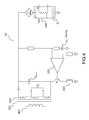
- FIG. 2 presents a functional block diagram depicting an electronic power conditioner or EPC comprised in a flexible travelling wave tube amplifier, or TWTA, according to an exemplary embodiment of the current invention.
- a flexible TWTA comprises primary power control means 20 driving high-voltage generation and control means 22, and interfacing with flexibility control means 24.
- the primary power control means 20 receive primary power from a primary power bus, and comprise a power cell 200 ensuring the control of the primary side of a high voltage transformer 220 described hereafter, and thus manage the power regulation, for example through two nested loops, one current control loop 204 driving the power cell through pulse width modulation, the current control loop 204 being driven by current sensing means 202, and by a voltage control loop 206. It is one specificity of the current invention that the voltage control loop 206 can be driven by an adjustable voltage reference 208. The means for adjusting the voltage reference 208 are comprised in the flexibility control means 24 and described further hereinafter. The primary power control means 20 then drive the high-voltage generation and control means 22. An exemplary embodiment of a high voltage generation and control module is described hereinafter by reference to Figure 4 .
- the high-voltage generation and control means 22 comprise a multistage high voltage transformer 220.
- the multistage high voltage transformer 220 can further comprise rectifiers and filters.
- the multistage high voltage transformer 220 generates the high voltages requested by a travelling wave tube 226; notably, the multistage high voltage transformer 220 can generate a plurality i of voltages for the plurality i of collectors C i ; besides, the high voltage transformer 220 can as well generate the "Anode 0" electrode voltage A0, and possibly an "Anode 1 " electrode voltage A1 allowing adjusting the emitted power, through regulators not shown on the figure.
- the helix to cathode voltage V KH can be supplied through a regulator 222 attached to the secondary side of the multistage high voltage transformer 220, and driven by a helix to cathode voltage setting module 224.
- the helix to cathode voltage V KH setting module 224 is adjusted to a helix to cathode voltage reference 244 that is comprised in the flexibility control means 24.
- the helix to cathode voltage reference 244 can for instance comprise a DAC, and an exemplary embodiment thereof is described further below in reference to Figure 5 .
- the flexibility control means 24 further comprises an n-bit decoder 240 receiving binary words from a data bus.
- the data bus can for instance be the communication data bus that is usually present onboard telecommunication satellites.
- the decoder 240 can generate a n-bit binary word output towards the helix to cathode voltage reference 244, as well as an m-bit (m being lower than n) word towards the voltage reference 208 referred to above, through a grounding isolation module 242.
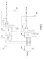
- Figure 3 presents a simplified electrical diagram depicting an EPC that is part of a flexible linearized travelling wave amplifier according to an exemplary embodiment of the current invention.
- An EPC 300 comprises an input filter 302 that interfaces with the power bus of the satellite, presenting a voltage V Bus .
- the input filter 302 is then attached to an inverter 306 through a Buck type regulator 304 forming part of the power cell 200 described above in reference to Figure 2 .
- the Buck type regulator 304 for example implements typical components such as a buck switching cell comprising a switching transistor 3041 and a free wheel diode 3042, an output filter based on a buck inductance 3044 associated to an output capacitor 3045.
- a dedicated current measurement for example based on a resistor 3043, can be used for the purpose of a back current control loop 3055.
- the buck type regulator power cell formed by the switching transistor 3041 and the free wheel diode 3042 may be driven by a dedicated regulation electronics comprised in a regulation module 305.
- control signals from the regulation loop can be digitalized, for example by a comparator 3052 comparing the signal with a dedicated sawtooth signal 3053, and providing the pulse width modulation command to the buck transistor 3041 grid through a dedicated driver 3051, then possibly through a grid resistor 3059.
- the regulation module 305 implements the nested voltage control loop 206 and current control loop 204 cited below by reference to Figure 2 .
- Regulation electronics comprised in the module 305 can be based on a back current control loop 3055 driven by an output voltage loop.
- the voltage loop may comprise a resistor bridge 3057, 3058 providing the measurement of the buck output voltage, that can be compared to the setting voltage V KCI , for example through an error amplifier comprised in a voltage control loop block 3056.
- the gain of the voltage control loop can be controlled by a dedicated gain control block K v 3054.
- the voltage control loop output signal may be used as a reference for the current control loop.
- a Zener diode V limit comprised in the voltage control loop may provide adequate clamping of the voltage control loop signal output and consequently fix the maximum value allowed by the current control loop.
- the regulation module 305 can further comprise voltage control adjustment means 3056, operating of which is described in details hereafter by reference to Figure 5 .
- the inverter 306 is attached to a high voltage transformer 308 that forms or is part of the multistage high voltage transformer 220 cited below in reference to Figure 2 .
- a high voltage signal reshaping module 310 is attached to the high voltage transformer 308, and aims at providing high DC voltages requested by a TWT 312.
- the high voltage signal reshaping module 310 can for example contain high voltage capacitors and bridge diodes.
- the TWT 312 comprises an RF signal input, and outputs an output RF signal to an RF load 314.
- Figure 4 presents a simplified electrical diagram depicting part of the high voltage stage of an EPC that is part of a flexible linearized travelling wave amplifier according to an exemplary embodiment of the current invention.
- a high voltage generation and control module 40 implementing high voltage generation and control means 22 by reference to Figure 2 comprises at its input the secondary side 402 of the high voltage transformer 220. Specific outputs of the secondary side 402 can be directly routed to the collectors C i of the TWT after rectifying and filtering. Each collector is associated with its dedicated winding, as well as notably its filtering capacitor. The sum of the capacitances of the capacitors dedicated to all collectors C i is represented on the figure as an equivalent capacitance C equiv . Also, a rectifying diode D is represented on the figure in series with the secondary side 402 of the high voltage transformer 220, and in parallel with the equivalent capacitance C equiv branch.
- the secondary side 402 can also be connected to a helix voltage accuracy controller V3, driven by the regulator 222.
- the helix voltage controller V3 is attached to a dissipating element 403, itself for example attached to the ground.
- the regulator 222 is driven by the helix to cathode voltage V KH setting.
- the helix voltage accuracy controller V3 can be formed by a bipolar transistor, whose emitter is attached to the dissipating element 403, which can itself be formed by a resistance.
- the collector of the bipolar transistor is then attached to the secondary side 402 of the high voltage transformer 220.
- the helix to cathode voltage V KH setting can for example be done through adjusting the voltage of a Zener diode through appropriate voltage adjustment means.
- the current invention proposes to transfer a part of the flexibility range directly to the primary side 401 of the high voltage transformer 220, through the control of the primary power converter 20, for example through the Buck type regulator 304, by reference to Figure 3 .
- directly providing the full range of flexibility to the helix voltage through the regulator 222 imposes a high stress on the helix voltage controller V3, and induces excessive dissipations.
- the high voltage components are usually enclosed in an isolating resin aiming at preventing any risks of burst that may occur due to arking phenomena.
- This can be alleviated thanks to the lowering of the voltage at the primary side 401 of the high voltage transformer 220, which can for example be achieved through adjusting the primary power converter 20, for example through the Buck type regulator 304.
- Adjusting the primary power converter 20 can be done through the regulation module 305, by reference to Figure 3 , and more specifically a reference voltage V KCI adjusting means, for example formed by a Zener diode whose voltage can be adjusted through appropriate means.
- the buck regulator setting voltage V KCI is acting on the primary side 401, and subsequently on all collector C i voltages, through their dedicated windings.
- the high voltage transformer 220 output voltages can be changed in the same proportion, provided a ratio V KH /V KCi between the helix to cathode voltage and the collector voltages constant, while reducing the level of stress on the helix series regulator 222.
- a constant ratio V KH /V KCi between the helix to cathode voltage and the collector voltages allows ensuring stability of the TWT and is particularly advantageous for an operation over a wide range of helix to cathode voltages, for instance over a range higher than 50 Volts with a TWT operating in the Ku band.
- Another advantage of keeping this ratio constant lies in the fact it allows keeping the output of the TWT (that is: the ratio between the RF power and the consumed power) essentially constant over the whole range of operation.
- Figure 5 presents a simplified electrical diagram depicting a flexibility control module, comprised in a flexible linearized travelling wave amplifier according to an exemplary embodiment of the current invention.
- a flexibility control module 50 can in an exemplary embodiment comprise the decoder 240 receiving control data through the data bus, and outputting two binary words.
- Input control binary words can be n-bit words, and the decoder 240 can forward one V KH setting control word to a first DAC 504 attached to a first shaping circuit 505, so as to generate an analog setting value for the helix to cathode reference voltage V KH ; in parallel, the decoder 240 can issue one V KCI setting control word to a second DAC 506, for example through a galvanic insulator 503, the second DAC 506 being also attached to a second shaping circuit 507, generating an analog setting value for the Buck regulator reference voltage V KCI .
- the first and second shaping circuits 505, 507 can for example comprise amplifiers and filters.
- the data bus may input 8-bit control words to the decoder 240.
- the decoder can for example forward the 8-bit control words to the first DAC 504, and send 4-bit words, for example consisting of the four most significant bits of the 8-bit word, to the second DAC 506.
- the Buck type regulator reference voltage is set proportionally and with a lower resolution, compared to the helix to cathode reference voltage V KH .
- the set point can be forced, when switching on the EPC, to the middle value of the flexibility range, in order to avoid any stress on the TWT 226 during the transient phase.
- an EPC 300 may provide control of the helix voltage up to 8 kilovolts through remote commands via the onboard communication databus of the satellite, together with simultaneous control of the collector high voltages, ranging from 500 to 3500 Volts, while keeping the TWT efficient.
- the helix voltage can for example be set flexible within a range of 0 to 550 Volts around the nominal operating point, with a resolution lower than 2.5 Volts as afforded by an 8-bit control word. It shall be observed here that the nominal set operating point can be typically varied between 2.5 and 7.7 kilovolts, depending upon the frequency band requested by the intended application - for example in C-band, Ku-band Ka-band, etc.
- the fine resolution thus achieved for adjusting the helix to cathode voltage allows a fine adaptation of the TWT phase response, typically in the order of about 1 degree per volt, and hence provides the opportunity of a fine tuning of the output RF signal phase.
Abstract
Description
- The current invention relates to a very high efficiency flexible travelling wave amplifier. It notably applies to telecommunication satellites.
- Telecommunication satellites usually comprise a platform and a payload, the latter being comprising all equipments, notably all devices intended for generating and transmitting high power radiofrequency signals - hereinafter referred to as RF signals - toward the ground. Different known techniques are resorted to for transmitting high power RF signals.
- A first technique is based on the solid state technology, and involves Solid State Power Amplifiers, usually referred to as SSPAs. SSPAs notably have the drawback of not being in a position to manage usually requested levels of RF power.
- A second technique is based on the use of Travelling Wave Tube Amplifiers, hereinafter referred to as TWTAs. TWTAs notably comprise a Travelling Wave Tube, hereinafter referred to as TWT. Telecommunication satellite payloads nowadays extensively use TWTAs. TWTAs are particularly efficient devices for high power RF transmission channels, and allow for managing very high levels of transmitted RF power. However, TWTA relies on a tube-based technology which requests a very precise tuning, not only on the manufacturing level, but also as regard to the accuracy of electrical interfaces. A TWT is described in much detail below in reference to
Figure 1 , and basically comprises an RF input and an RF output, a helix, and electrodes comprising a cathode emitting electrons forming an electron beam, an anode, usually referred to as "Anode Zero" or "Anode 0", focussing the electron beam, and a plurality of collectors. - Moreover, each produced TWTA is unique, and optimized for the purpose of a unique application, in terms of transmitted frequency, level of transmitted power and efficiency. Once designed, manufactured and possibly optimized, a TWTA and its associated control equipment have to keep operating the same way all through a satellite's assembly, integration and testing, and the in-flight mission of the satellite they are set in. That is: once the telecommunication satellite has been assembled, these equipments shall be operated under the specific conditions they have been designed for. Besides, the efficiency performance of TWTAs is frequency-dependent. Therefore, in parallel, a satellite intended for transmitting through a plurality of channels, shall be containing as many TWTAs, with related consequences in terms of cost, weight and bulk. Also, one TWTA being usually destined to transmit through one given channel over a typical mission duration of more than 15 years makes the payload design and the TWTA procurement very constraining and induces severe constraints in terms of risk management.
- Wide-band TWTAs are known in the prior art, but existing devices typically suffer an efficiency degradation of about 2 percents compared to analogue TWTAs optimized in a narrower RF band.
- For all above-mentioned reasons, a very long and costly part of a telecommunication satellite payload development is to propose a technical answer to the final customer needs, in terms of number of channels, frequency and power allocation, minimizing the power demand to the platform and within given reliability requirements.
- One aim of the current invention is to palliate at least the above-mentioned drawbacks, by proposing a TWTA presenting an efficiency similar to that of known tuned narrow band TWTAs, while being able to be operated over a large variety of frequencies, as a wide band TWTA.
- One further advantage of the current invention is that the TWTA offers the ability of being easily controlled not only on ground, but also during in-flight operations over a satellite mission.
- One further advantage of the current invention is that a TWTA according to one of the described embodiments uses control electronics that can be adaptable for any existing high voltage electronic circuitry.
- One further advantage of the current invention is that it alleviates resorting to redundancy of onboard TWTs for given applications, as all TWTs controlled within TWTAs following embodiments of the current invention, can be operated over a wide band.
- One further advantage of the current invention is that it allows mission profile adaptation throughout the satellite payload life, without affecting the global payload efficiency.
- One further advantage of the current invention is that it offers a phase flexibility affording the opportunity to replace phase shifter dedicated hardware in certain applications.
- All the advantages cited below do present benefits in terms of schedule, weight, cost and optimization of failure management.
- For that purpose, the current invention proposes a travelling wave tube amplifier comprising at least a travelling wave tube comprising a cathode, a helix, an RF input, an RF output, and a plurality of collectors Ci; an electronic power conditioner providing power supply and electrode polarization to said travelling wave tube; the travelling wave tube amplifier being characterized in that said electronic power conditioner comprises flexibility control means allowing to adjust, via control commands, the helix to cathode voltage, so as to allow adjusting the TWT operating frequency within a determined range with an optimal efficiency.
- In an exemplary embodiment of the present invention, the flexibility control means can also be configured to adjust the collector Ci voltages, the ratio between the helix to cathode voltage and collector Ci voltages remaining constant.
- In an exemplary embodiment of the present invention, the control commands can be sent through a databus.
- In an exemplary embodiment of the present invention, the electronic power conditioner can comprise primary control means comprising a power cell driving a high voltage generation and control means comprising a multistage high voltage transformer whose primary side is controlled by said power cell and generating the high voltages requested by said at least one collector, cathode and helix, said flexibility control means comprising means for adjusting a voltage reference driving a voltage control loop, said voltage control loop being driving the power cell through pulse width modulation.
- In an exemplary embodiment of the present invention, the high voltage generation and control means can comprise a regulator attached to the secondary side of said multistage high voltage transformer and supplying a helix to cathode voltage, being adjusted to a helix to cathode voltage reference comprised in said flexibility control means.
- In an exemplary embodiment of the present invention, the flexibility control means can further comprise a decoder issuing signal control words from said control commands, and said helix to cathode voltage reference can comprise a first digital-to-analog converter converting binary output words generated by a decoder based upon input binary words sent via said databus.
- In an exemplary embodiment of the present invention, said means for adjusting the voltage reference can comprise a second digital-to-analog converter converting binary output words generated by the decoder based upon input binary words sent via said databus.
- In an exemplary embodiment of the present invention, said decoder can generate n-bit output words towards the helix to cathode voltage reference, and m-bit output words, m being lower than n, towards the means for adjusting the voltage reference, based upon n-bit input words received from the databus.
- In an exemplary embodiment of the present invention, the number m of bits of the output words towards the means for adjusting the voltage reference can be chosen so as to allow adjusting the RF signal phase.
- In an exemplary embodiment of the present invention, the high voltage generation and control means can be implemented within a high voltage generation and control module comprising at its input the secondary side of the high voltage transformer also connected to a helix voltage accuracy controller formed by a bipolar transistor driven by the regulator, and whose emitter is attached to the ground through a dissipating element.
- These and other characteristics and advantages of the invention will be made clearer in view of the detailed description given below of a preferred embodiment, provided by way of an illustrative and non-limiting example only, as well as the accompanying drawings which represent:
-
Figure 1 , a perspective view depicting a typical TWT known in the prior art; -
Figure 2 , a functional block diagram depicting an electronic power conditioner or EPC comprised in a flexible travelling wave tube amplifier, or TWTA, according to an exemplary embodiment of the current invention; -
Figure 3 , a simplified electrical diagram depicting an EPC that is part of a flexible travelling wave amplifier according to an exemplary embodiment of the current invention; -
Figure 4 , a simplified electrical diagram depicting part of the high voltage stage of an EPC that is part of a flexible TWTA according to an exemplary embodiment of the current invention; -
Figure 5 , a simplified electrical diagram depicting a flexibility control module, comprised in a flexible TWTA according to an exemplary embodiment of the current invention. -
Figure 1 presents a perspective view depicting a typical TWT known in the prior art. A TWT is one of the key elements comprised in a TWTA. - A TWT 10 is basically an elongated vacuum tube comprising a radiofrequency input 12 and a radiofrequency output 14, a cathode 15 forming an electron gun generating an electron beam 17 focused and adjusted by an Anode Zero 13 passing through a helix 18 up to a plurality of collectors 19.
- The cathode 15 is heated and emits electrons at one of its ends. A magnetic field is generated substantially around the helix 18 so as to contain the electrons as the focused electron beam 17. The electron beam passes through along the middle axis of the helix 18. The helix 18 is extending from the RF input 12 to the RF output 14. The electron beam 17 is finally striking the collectors 19. The RF signal travels along the helix 18 at a speed that is close to that of the electron beam 17. The amplification effect is due to the interaction between the electromagnetic field induced by the RF signal in the helix 18, and the electron beam 17 through a quantum phenomenon. For the purpose of improving the TWT yield in terms of energy, that is: optimizing recycling of the energy still available at the end of the electron beam 17, a plurality of collectors 19, typically: four or five, may be employed.
- A TWTA usually comprises a TWT, associated with an additional Electronic Power Conditioner, hereinafter referred to as EPC, whose purpose is to supply the TWT with requested electrical operational conditions. The EPC is usually a DC-DC converter supplied in energy through a bus, and generating the voltage supply levels requested on each of the electrodes comprised in the TWT, with an accuracy level allowing to ensure the TWT performances, that is: the efficiency and the stability of the power transfer. Particularly, the high voltage between helix 18 and cathode 15 shall be enough accurate, as it is determining the TWT performance. Indeed, as for the helix - cathode voltage: accuracies on the order of 1 Volt are required, for voltages ranking up to several kilovolts; for instance, the required voltages between the helix and the cathode for applications within the Ku band is typically on the order of 6 kilovolts to 7.5 kilovolts. Control of said voltage levels is managed by the EPC.
- The electrode referred to as Anode Zero 13 or "Anode 0", allows controlling the electron beam 17 generated by the cathode 15.
- One particular type of TWTA is commonly referred to as LTWTA, standing for "Linearized TWTA". LTWTAs comprise an additional linearized preamplifier aiming at conditioning the RF signal level with the RF input 12 and providing compensation to spurious nonlinearity phenomena notably brought by the TWT. The embodiments of the current invention described hereinafter may notably apply to both types of TWTAs.
- Usually, for TWTs already known in the prior art, the TWT manufacturers specify polarization parameters to the EPC according to the tuning parameters of the tube. Especially the helix voltage fixes the frequency operating point, while collector voltages are tuned so as to optimize the global TWT efficiency. As soon as the TWTA operating point is fixed, the TWTA cannot be operated in safe and efficient conditions at another frequency than one for which the operating point has been tuned. The present invention proposes to confer flexibility to the TWTA by controlling the helix voltage value within a range fixed by the awaited frequency excursion, together with the relevant correction of the collector voltages in order to maintain the optimum of efficiency. Controlling may for instance be done on ground level, prior to the launch of a mission, but also throughout the satellite in-flight mission, remotely, for example through the satellite onboard communication databus.
- While the control of the helix voltage over the full range of flexibility allows for instance to transfer the TWT operating frequency from the lower part of the allowed RF band to the higher part - or inversely - the resolution of the control also allows to provide small variations of the RF signal phase resulting from the relevant voltage variation. Hence the proposed flexibility also offers the opportunity to correct the TWT output phase, which is a feature that may be especially useful in Multi Port Amplifiers, commonly referred to under the acronym MPA, where parallelized TWTAs require very accurate phase tuning, which usually resorts to costly phase shifter devices. MPAs allow generating more powerful signals by adding phase-coherent signals generated by a plurality of parallelized TWTAs.
- According to the current invention, it is possible to adapt the helix to cathode voltage so as to allow an optimal efficiency, regardless of possible variations of the TWT operating frequency and proposes to control the collector voltages simultaneously with controlling the helix to cathode voltage through dedicated controls, in order to keep the amplifier efficiency optimal.
- The present invention can be realized through appropriate means implemented within the EPC of a TWTA.
-
Figure 2 presents a functional block diagram depicting an electronic power conditioner or EPC comprised in a flexible travelling wave tube amplifier, or TWTA, according to an exemplary embodiment of the current invention. - In a non-limitative example illustrated by the figure, a flexible TWTA comprises primary power control means 20 driving high-voltage generation and control means 22, and interfacing with flexibility control means 24.
- The primary power control means 20 receive primary power from a primary power bus, and comprise a power cell 200 ensuring the control of the primary side of a high voltage transformer 220 described hereafter, and thus manage the power regulation, for example through two nested loops, one current control loop 204 driving the power cell through pulse width modulation, the current control loop 204 being driven by current sensing means 202, and by a voltage control loop 206. It is one specificity of the current invention that the voltage control loop 206 can be driven by an adjustable voltage reference 208. The means for adjusting the voltage reference 208 are comprised in the flexibility control means 24 and described further hereinafter. The primary power control means 20 then drive the high-voltage generation and control means 22. An exemplary embodiment of a high voltage generation and control module is described hereinafter by reference to
Figure 4 . - At its input level, the high-voltage generation and control means 22 comprise a multistage high voltage transformer 220. The multistage high voltage transformer 220 can further comprise rectifiers and filters. The multistage high voltage transformer 220 generates the high voltages requested by a travelling wave tube 226; notably, the multistage high voltage transformer 220 can generate a plurality i of voltages for the plurality i of collectors Ci; besides, the high voltage transformer 220 can as well generate the "Anode 0" electrode voltage A0, and possibly an "Anode 1 " electrode voltage A1 allowing adjusting the emitted power, through regulators not shown on the figure. It is one other specificity of the current invention, that the helix to cathode voltage VKH can be supplied through a regulator 222 attached to the secondary side of the multistage high voltage transformer 220, and driven by a helix to cathode voltage setting module 224. The helix to cathode voltage VKH setting module 224 is adjusted to a helix to cathode voltage reference 244 that is comprised in the flexibility control means 24. The helix to cathode voltage reference 244 can for instance comprise a DAC, and an exemplary embodiment thereof is described further below in reference to
Figure 5 . - The flexibility control means 24 further comprises an n-bit decoder 240 receiving binary words from a data bus. The data bus can for instance be the communication data bus that is usually present onboard telecommunication satellites. The decoder 240 can generate a n-bit binary word output towards the helix to cathode voltage reference 244, as well as an m-bit (m being lower than n) word towards the voltage reference 208 referred to above, through a grounding isolation module 242.
-
Figure 3 presents a simplified electrical diagram depicting an EPC that is part of a flexible linearized travelling wave amplifier according to an exemplary embodiment of the current invention. - An EPC 300 comprises an input filter 302 that interfaces with the power bus of the satellite, presenting a voltage VBus. The input filter 302 is then attached to an inverter 306 through a Buck type regulator 304 forming part of the power cell 200 described above in reference to
Figure 2 . The Buck type regulator 304 for example implements typical components such as a buck switching cell comprising a switching transistor 3041 and a free wheel diode 3042, an output filter based on a buck inductance 3044 associated to an output capacitor 3045. A dedicated current measurement, for example based on a resistor 3043, can be used for the purpose of a back current control loop 3055. The buck type regulator power cell formed by the switching transistor 3041 and the free wheel diode 3042 may be driven by a dedicated regulation electronics comprised in a regulation module 305. In the regulation module 305, control signals from the regulation loop can be digitalized, for example by a comparator 3052 comparing the signal with a dedicated sawtooth signal 3053, and providing the pulse width modulation command to the buck transistor 3041 grid through a dedicated driver 3051, then possibly through a grid resistor 3059. The regulation module 305 implements the nested voltage control loop 206 and current control loop 204 cited below by reference toFigure 2 . - Regulation electronics comprised in the module 305 can be based on a back current control loop 3055 driven by an output voltage loop. The voltage loop may comprise a resistor bridge 3057, 3058 providing the measurement of the buck output voltage, that can be compared to the setting voltage VKCI, for example through an error amplifier comprised in a voltage control loop block 3056. The gain of the voltage control loop can be controlled by a dedicated gain control block Kv 3054. The voltage control loop output signal may be used as a reference for the current control loop. A Zener diode Vlimit comprised in the voltage control loop may provide adequate clamping of the voltage control loop signal output and consequently fix the maximum value allowed by the current control loop.
- According to one specificity of the current invention, the regulation module 305 can further comprise voltage control adjustment means 3056, operating of which is described in details hereafter by reference to
Figure 5 . - The inverter 306 is attached to a high voltage transformer 308 that forms or is part of the multistage high voltage transformer 220 cited below in reference to
Figure 2 . A high voltage signal reshaping module 310 is attached to the high voltage transformer 308, and aims at providing high DC voltages requested by a TWT 312. The high voltage signal reshaping module 310 can for example contain high voltage capacitors and bridge diodes. The TWT 312 comprises an RF signal input, and outputs an output RF signal to an RF load 314. -
Figure 4 presents a simplified electrical diagram depicting part of the high voltage stage of an EPC that is part of a flexible linearized travelling wave amplifier according to an exemplary embodiment of the current invention. - A high voltage generation and control module 40 implementing high voltage generation and control means 22 by reference to
Figure 2 , comprises at its input the secondary side 402 of the high voltage transformer 220. Specific outputs of the secondary side 402 can be directly routed to the collectors Ci of the TWT after rectifying and filtering. Each collector is associated with its dedicated winding, as well as notably its filtering capacitor. The sum of the capacitances of the capacitors dedicated to all collectors Ci is represented on the figure as an equivalent capacitance Cequiv. Also, a rectifying diode D is represented on the figure in series with the secondary side 402 of the high voltage transformer 220, and in parallel with the equivalent capacitance Cequiv branch. The secondary side 402 can also be connected to a helix voltage accuracy controller V3, driven by the regulator 222. The helix voltage controller V3 is attached to a dissipating element 403, itself for example attached to the ground. The regulator 222 is driven by the helix to cathode voltage VKH setting. The helix voltage accuracy controller V3 can be formed by a bipolar transistor, whose emitter is attached to the dissipating element 403, which can itself be formed by a resistance. The collector of the bipolar transistor is then attached to the secondary side 402 of the high voltage transformer 220. The helix to cathode voltage VKH setting can for example be done through adjusting the voltage of a Zener diode through appropriate voltage adjustment means. - The current invention proposes to transfer a part of the flexibility range directly to the primary side 401 of the high voltage transformer 220, through the control of the primary power converter 20, for example through the Buck type regulator 304, by reference to
Figure 3 . Indeed, directly providing the full range of flexibility to the helix voltage through the regulator 222 imposes a high stress on the helix voltage controller V3, and induces excessive dissipations. It shall be observed here that the high voltage components are usually enclosed in an isolating resin aiming at preventing any risks of burst that may occur due to arking phenomena. For instance, if the helix to cathode voltage has to be controlled over a very large range, that would impose too much thermal energy to be dissipated, then the stress on the helix voltage controller V3. This can be alleviated thanks to the lowering of the voltage at the primary side 401 of the high voltage transformer 220, which can for example be achieved through adjusting the primary power converter 20, for example through the Buck type regulator 304. Adjusting the primary power converter 20 can be done through the regulation module 305, by reference toFigure 3 , and more specifically a reference voltage VKCI adjusting means, for example formed by a Zener diode whose voltage can be adjusted through appropriate means. In other words, the buck regulator setting voltage VKCI is acting on the primary side 401, and subsequently on all collector Ci voltages, through their dedicated windings. - Advantageously, the high voltage transformer 220 output voltages can be changed in the same proportion, provided a ratio VKH/VKCi between the helix to cathode voltage and the collector voltages constant, while reducing the level of stress on the helix series regulator 222. Keeping a constant ratio VKH/VKCi between the helix to cathode voltage and the collector voltages allows ensuring stability of the TWT and is particularly advantageous for an operation over a wide range of helix to cathode voltages, for instance over a range higher than 50 Volts with a TWT operating in the Ku band. Another advantage of keeping this ratio constant lies in the fact it allows keeping the output of the TWT (that is: the ratio between the RF power and the consumed power) essentially constant over the whole range of operation.
-
Figure 5 presents a simplified electrical diagram depicting a flexibility control module, comprised in a flexible linearized travelling wave amplifier according to an exemplary embodiment of the current invention. - A flexibility control module 50, implementing flexibility control means 24 as described below by reference to
Figure 2 , can in an exemplary embodiment comprise the decoder 240 receiving control data through the data bus, and outputting two binary words. Input control binary words can be n-bit words, and the decoder 240 can forward one VKH setting control word to a first DAC 504 attached to a first shaping circuit 505, so as to generate an analog setting value for the helix to cathode reference voltage VKH; in parallel, the decoder 240 can issue one VKCI setting control word to a second DAC 506, for example through a galvanic insulator 503, the second DAC 506 being also attached to a second shaping circuit 507, generating an analog setting value for the Buck regulator reference voltage VKCI. The first and second shaping circuits 505, 507 can for example comprise amplifiers and filters. - As a more specific example, the data bus may input 8-bit control words to the decoder 240. The decoder can for example forward the 8-bit control words to the first DAC 504, and send 4-bit words, for example consisting of the four most significant bits of the 8-bit word, to the second DAC 506. Thus, the Buck type regulator reference voltage is set proportionally and with a lower resolution, compared to the helix to cathode reference voltage VKH.
- Advantageously, the set point can be forced, when switching on the EPC, to the middle value of the flexibility range, in order to avoid any stress on the TWT 226 during the transient phase.
- For example, an EPC 300 may provide control of the helix voltage up to 8 kilovolts through remote commands via the onboard communication databus of the satellite, together with simultaneous control of the collector high voltages, ranging from 500 to 3500 Volts, while keeping the TWT efficient. The helix voltage can for example be set flexible within a range of 0 to 550 Volts around the nominal operating point, with a resolution lower than 2.5 Volts as afforded by an 8-bit control word. It shall be observed here that the nominal set operating point can be typically varied between 2.5 and 7.7 kilovolts, depending upon the frequency band requested by the intended application - for example in C-band, Ku-band Ka-band, etc. It shall be observed that the fine resolution thus achieved for adjusting the helix to cathode voltage allows a fine adaptation of the TWT phase response, typically in the order of about 1 degree per volt, and hence provides the opportunity of a fine tuning of the output RF signal phase.
Claims (10)
- Travelling wave tube amplifier comprising at least:• a travelling wave tube (10, 226) comprising a cathode (15), a helix (18), an RF input (12), an RF output (14), and a plurality of collectors Ci (19),• an electronic power conditioner (300) providing power supply and electrode polarization to said travelling wave tube (10, 226),characterized in that said electronic power conditioner (300) comprises flexibility control means (24) adjusting, via control commands, the helix to cathode voltage so as to allow adjusting the travelling wave tube (10, 226) operating frequency range.
- Travelling wave tube amplifier following claim 1, wherein said flexibility control means are also configured to adjust the collector Ci voltages, the ratio between the helix to cathode voltage and collector C; voltages remaining constant.
- Travelling wave tube amplifier following any of preceding claims, wherein said control commands are sent through a databus.
- Travelling wave tube amplifier following any of preceding claims, wherein the electronic power conditioner (300) comprises primary control means (20) comprising a power cell (200) driving a high voltage generation and control means (22) comprising a multistage high voltage transformer (220), whose primary side is controlled by said power cell (200) and generating the high voltages requested by said at least one collector (19), cathode (15) and helix (18), said flexibility control means (24) comprising means for adjusting a voltage reference (208) driving a voltage control loop (206), said voltage control loop (206) being driving the power cell (200) through pulse width modulation.
- Travelling wave tube amplifier following Claim 4, wherein the high voltage generation and control means (22) comprise a regulator (222) attached to the secondary side (402) of said multistage high voltage transformer (220) and supplying a helix to cathode voltage (VKH), being adjusted to a helix to cathode voltage reference (244) comprised in said flexibility control means (24).
- Travelling wave tube amplifier following Claim 5, wherein flexibility control means (24) further comprise a decoder (240) issuing signal control words from said control commands, said helix to cathode voltage reference (244) comprising a first digital-to-analog converter (504) converting binary output words generated by the decoder (240) into an analog signal controlling the helix to cathode voltage (VKH).
- Travelling wave tube amplifier following Claim 4, wherein said means for adjusting the voltage reference (208) comprises a second digital-to-analog converter (506) converting binary output words generated by the decoder (240) based upon input binary words sent via said databus.
- Travelling wave tube amplifier following any of preceding Claims 6 and 7, wherein said decoder (240) generates n-bit output words towards the helix to cathode voltage reference (244), and m-bit output words, m being lower than n, towards the means for adjusting the voltage reference (208), based upon n-bit input words received from the databus.
- Travelling wave tube amplifier following Claim 8, wherein the number m of bits of the output words towards the means for adjusting the voltage reference (208) is chosen so as to allow adjusting the RF signal phase.
- Travelling wave tube amplifier following any of preceding Claims 5 to 9, wherein high voltage generation and control means (22) are implemented within a high voltage generation and control module (40) comprising at its input the secondary side (402) of the high voltage transformer (220) also connected to a helix voltage accuracy controller (V3) formed by a bipolar transistor driven by the regulator (222), and whose emitter is attached to the ground through a dissipating element (403).
Priority Applications (1)
| Application Number | Priority Date | Filing Date | Title |
|---|---|---|---|
| EP11186209.0A EP2445104B2 (en) | 2010-10-22 | 2011-10-21 | Very high efficiency flexible travelling wave amplifier |
Applications Claiming Priority (2)
| Application Number | Priority Date | Filing Date | Title |
|---|---|---|---|
| EP10290571A EP2445102A1 (en) | 2010-10-22 | 2010-10-22 | Very high efficiency flexible travelling wave amplifier |
| EP11186209.0A EP2445104B2 (en) | 2010-10-22 | 2011-10-21 | Very high efficiency flexible travelling wave amplifier |
Publications (4)
| Publication Number | Publication Date |
|---|---|
| EP2445104A2 true EP2445104A2 (en) | 2012-04-25 |
| EP2445104A3 EP2445104A3 (en) | 2012-10-10 |
| EP2445104B1 EP2445104B1 (en) | 2013-08-21 |
| EP2445104B2 EP2445104B2 (en) | 2017-02-01 |
Family
ID=43858193
Family Applications (2)
| Application Number | Title | Priority Date | Filing Date |
|---|---|---|---|
| EP10290571A Withdrawn EP2445102A1 (en) | 2010-10-22 | 2010-10-22 | Very high efficiency flexible travelling wave amplifier |
| EP11186209.0A Active EP2445104B2 (en) | 2010-10-22 | 2011-10-21 | Very high efficiency flexible travelling wave amplifier |
Family Applications Before (1)
| Application Number | Title | Priority Date | Filing Date |
|---|---|---|---|
| EP10290571A Withdrawn EP2445102A1 (en) | 2010-10-22 | 2010-10-22 | Very high efficiency flexible travelling wave amplifier |
Country Status (6)
| Country | Link |
|---|---|
| US (1) | US8742840B2 (en) |
| EP (2) | EP2445102A1 (en) |
| JP (1) | JP5877422B2 (en) |
| CN (1) | CN102571008B (en) |
| ES (1) | ES2432101T5 (en) |
| RU (1) | RU2564632C2 (en) |
Families Citing this family (5)
| Publication number | Priority date | Publication date | Assignee | Title |
|---|---|---|---|---|
| DE102013002477B4 (en) * | 2013-02-14 | 2019-01-10 | Tesat-Spacecom Gmbh & Co.Kg | Control device for a transmission amplifier element |
| GB201518859D0 (en) | 2015-10-23 | 2015-12-09 | Airbus Defence & Space Ltd | High-efficiency amplifier |
| CN109302065A (en) * | 2018-09-12 | 2019-02-01 | 合肥雷科电子科技有限公司 | A kind of millimeter wave traveling wave tube MPM power module |
| CN109995334B (en) * | 2019-03-29 | 2024-02-09 | 成都四威功率电子科技有限公司 | Overshoot eliminating device for output radio frequency pulse signal of traveling wave tube pulse power amplifier |
| KR102088041B1 (en) * | 2019-10-11 | 2020-03-11 | 엘아이지넥스원 주식회사 | Output control device and method of adaptive traveling-wave tube amplifier for external operation environment |
Family Cites Families (14)
| Publication number | Priority date | Publication date | Assignee | Title |
|---|---|---|---|---|
| US5A (en) * | 1836-08-10 | Thomas blancharjq | ||
| US2A (en) * | 1826-12-15 | 1836-07-29 | mode of manufacturing wool or other fibrous materials | |
| US2619543A (en) * | 1950-07-11 | 1952-11-25 | Bell Telephone Labor Inc | Frequency changing pulse repeater employing phase modulation |
| US2811664A (en) * | 1952-10-31 | 1957-10-29 | Kazan Benjamin | Traveling wave thermionic tube |
| SU1107284A1 (en) * | 1982-03-01 | 1984-08-07 | Предприятие П/Я А-7162 | Pulse power amplifier based on travelling wave tube |
| RU2085022C1 (en) * | 1992-11-27 | 1997-07-20 | Научно-производственная фирма "Комкон" | Travelling wave tube power amplifier |
| US5500621A (en) * | 1995-04-03 | 1996-03-19 | Martin Marietta Corp. | Travelling-wave tube protection arrangement |
| JP3011127B2 (en) * | 1997-03-27 | 2000-02-21 | 日本電気株式会社 | Cold cathode electron gun and microwave tube for microwave tube |
| FR2837997B1 (en) | 2002-03-29 | 2005-03-04 | Thales Sa | METHOD FOR MEASURING MICROFREQUENCY TUBE AMPLIFIER POWER AND DEVICE FOR IMPLEMENTING THE METHOD |
| AU2003274497A1 (en) * | 2002-11-19 | 2004-06-15 | Koninklijke Philips Electronics N.V. | Travelling-wave amplifier |
| AU2004218611B2 (en) * | 2003-10-10 | 2007-03-08 | The Directv Group, Inc. | Coherent averaging for measuring traveling wave tube amplifier nonlinearity |
| US20090219087A1 (en) * | 2004-04-21 | 2009-09-03 | Francis Auvray | Travelling wave amplifier |
| US7579778B2 (en) * | 2006-07-11 | 2009-08-25 | L-3 Communications Electron Technologies, Inc. | Traveling-wave tube with integrated ion trap power supply |
| CN100596017C (en) * | 2007-01-31 | 2010-03-24 | 北京中科新微特科技开发有限公司 | Step travel wave amplifier circuit |
-
2010
- 2010-10-22 EP EP10290571A patent/EP2445102A1/en not_active Withdrawn
-
2011
- 2011-10-20 US US13/278,039 patent/US8742840B2/en active Active
- 2011-10-21 RU RU2011142691/08A patent/RU2564632C2/en active
- 2011-10-21 ES ES11186209.0T patent/ES2432101T5/en active Active
- 2011-10-21 EP EP11186209.0A patent/EP2445104B2/en active Active
- 2011-10-24 CN CN201110393414.1A patent/CN102571008B/en active Active
- 2011-10-24 JP JP2011232927A patent/JP5877422B2/en active Active
Non-Patent Citations (1)
| Title |
|---|
| None |
Also Published As
| Publication number | Publication date |
|---|---|
| US20120268201A1 (en) | 2012-10-25 |
| RU2564632C2 (en) | 2015-10-10 |
| RU2011142691A (en) | 2013-04-27 |
| CN102571008B (en) | 2016-04-20 |
| EP2445104A3 (en) | 2012-10-10 |
| CN102571008A (en) | 2012-07-11 |
| US8742840B2 (en) | 2014-06-03 |
| JP2012094517A (en) | 2012-05-17 |
| EP2445104B2 (en) | 2017-02-01 |
| ES2432101T5 (en) | 2017-07-12 |
| EP2445104B1 (en) | 2013-08-21 |
| EP2445102A1 (en) | 2012-04-25 |
| ES2432101T3 (en) | 2013-11-29 |
| JP5877422B2 (en) | 2016-03-08 |
Similar Documents
| Publication | Publication Date | Title |
|---|---|---|
| US8742840B2 (en) | Very high efficiency flexible travelling wave amplifier | |
| EP2445105B1 (en) | Power management system for dual travelling wave tube amplifier | |
| US5500621A (en) | Travelling-wave tube protection arrangement | |
| US7368874B2 (en) | Dynamic depressed collector | |
| US5781456A (en) | Software select and test | |
| US8488349B2 (en) | Method and apparatus for tracking power supplies | |
| US5469026A (en) | Method and apparatus for VF tube power supply | |
| US20060103460A1 (en) | System and Method for Envelope Modulation | |
| JP6267765B2 (en) | Power supply stage and method for generating output supply signal | |
| US9178475B2 (en) | Method for operating an amplifier module of a satellite | |
| JP2014158264A (en) | Control device of transmission amplifying element | |
| JP5743654B2 (en) | High frequency circuit system | |
| Jaumann | Improved flexibility by in-orbit-adjustable saturation output power of TWTs | |
| US20160182099A1 (en) | Systems and methods for efficient multi-channel satcom with dynamic power supply and digital pre-distortion | |
| KR102659157B1 (en) | Beamforming system and calibration method thereof | |
| US4727292A (en) | High voltage power supply fault isolation system | |
| US20180027641A1 (en) | X-Ray Source Controller | |
| Palz | Advanced space TWTA's for communications direct broadcast and earth remote sensing | |
| Kourmish et al. | High-power units for GALS R16 transponders | |
| Pelletier et al. | Ku-band modern TWTA's for satellite transponders |
Legal Events
| Date | Code | Title | Description |
|---|---|---|---|
| AK | Designated contracting states |
Kind code of ref document: A2 Designated state(s): AL AT BE BG CH CY CZ DE DK EE ES FI FR GB GR HR HU IE IS IT LI LT LU LV MC MK MT NL NO PL PT RO RS SE SI SK SM TR |
|
| AX | Request for extension of the european patent |
Extension state: BA ME |
|
| PUAI | Public reference made under article 153(3) epc to a published international application that has entered the european phase |
Free format text: ORIGINAL CODE: 0009012 |
|
| PUAL | Search report despatched |
Free format text: ORIGINAL CODE: 0009013 |
|
| AK | Designated contracting states |
Kind code of ref document: A3 Designated state(s): AL AT BE BG CH CY CZ DE DK EE ES FI FR GB GR HR HU IE IS IT LI LT LU LV MC MK MT NL NO PL PT RO RS SE SI SK SM TR |
|
| AX | Request for extension of the european patent |
Extension state: BA ME |
|
| RIC1 | Information provided on ipc code assigned before grant |
Ipc: H03F 3/58 20060101AFI20120906BHEP |
|
| GRAP | Despatch of communication of intention to grant a patent |
Free format text: ORIGINAL CODE: EPIDOSNIGR1 |
|
| 17P | Request for examination filed |
Effective date: 20130308 |
|
| INTG | Intention to grant announced |
Effective date: 20130416 |
|
| GRAS | Grant fee paid |
Free format text: ORIGINAL CODE: EPIDOSNIGR3 |
|
| GRAA | (expected) grant |
Free format text: ORIGINAL CODE: 0009210 |
|
| AK | Designated contracting states |
Kind code of ref document: B1 Designated state(s): AL AT BE BG CH CY CZ DE DK EE ES FI FR GB GR HR HU IE IS IT LI LT LU LV MC MK MT NL NO PL PT RO RS SE SI SK SM TR |
|
| REG | Reference to a national code |
Ref country code: GB Ref legal event code: FG4D |
|
| REG | Reference to a national code |
Ref country code: CH Ref legal event code: EP |
|
| REG | Reference to a national code |
Ref country code: AT Ref legal event code: REF Ref document number: 628594 Country of ref document: AT Kind code of ref document: T Effective date: 20130915 |
|
| REG | Reference to a national code |
Ref country code: IE Ref legal event code: FG4D |
|
| REG | Reference to a national code |
Ref country code: DE Ref legal event code: R096 Ref document number: 602011002690 Country of ref document: DE Effective date: 20131024 |
|
| REG | Reference to a national code |
Ref country code: NL Ref legal event code: VDEP Effective date: 20130821 Ref country code: AT Ref legal event code: MK05 Ref document number: 628594 Country of ref document: AT Kind code of ref document: T Effective date: 20130821 |
|
| REG | Reference to a national code |
Ref country code: LT Ref legal event code: MG4D |
|
| PG25 | Lapsed in a contracting state [announced via postgrant information from national office to epo] |
Ref country code: HR Free format text: LAPSE BECAUSE OF FAILURE TO SUBMIT A TRANSLATION OF THE DESCRIPTION OR TO PAY THE FEE WITHIN THE PRESCRIBED TIME-LIMIT Effective date: 20130821 Ref country code: PT Free format text: LAPSE BECAUSE OF FAILURE TO SUBMIT A TRANSLATION OF THE DESCRIPTION OR TO PAY THE FEE WITHIN THE PRESCRIBED TIME-LIMIT Effective date: 20131223 Ref country code: NO Free format text: LAPSE BECAUSE OF FAILURE TO SUBMIT A TRANSLATION OF THE DESCRIPTION OR TO PAY THE FEE WITHIN THE PRESCRIBED TIME-LIMIT Effective date: 20131121 Ref country code: LT Free format text: LAPSE BECAUSE OF FAILURE TO SUBMIT A TRANSLATION OF THE DESCRIPTION OR TO PAY THE FEE WITHIN THE PRESCRIBED TIME-LIMIT Effective date: 20130821 Ref country code: SE Free format text: LAPSE BECAUSE OF FAILURE TO SUBMIT A TRANSLATION OF THE DESCRIPTION OR TO PAY THE FEE WITHIN THE PRESCRIBED TIME-LIMIT Effective date: 20130821 Ref country code: IS Free format text: LAPSE BECAUSE OF FAILURE TO SUBMIT A TRANSLATION OF THE DESCRIPTION OR TO PAY THE FEE WITHIN THE PRESCRIBED TIME-LIMIT Effective date: 20131221 Ref country code: CY Free format text: LAPSE BECAUSE OF FAILURE TO SUBMIT A TRANSLATION OF THE DESCRIPTION OR TO PAY THE FEE WITHIN THE PRESCRIBED TIME-LIMIT Effective date: 20130821 Ref country code: AT Free format text: LAPSE BECAUSE OF FAILURE TO SUBMIT A TRANSLATION OF THE DESCRIPTION OR TO PAY THE FEE WITHIN THE PRESCRIBED TIME-LIMIT Effective date: 20130821 |
|
| PG25 | Lapsed in a contracting state [announced via postgrant information from national office to epo] |
Ref country code: FI Free format text: LAPSE BECAUSE OF FAILURE TO SUBMIT A TRANSLATION OF THE DESCRIPTION OR TO PAY THE FEE WITHIN THE PRESCRIBED TIME-LIMIT Effective date: 20130821 Ref country code: LV Free format text: LAPSE BECAUSE OF FAILURE TO SUBMIT A TRANSLATION OF THE DESCRIPTION OR TO PAY THE FEE WITHIN THE PRESCRIBED TIME-LIMIT Effective date: 20130821 Ref country code: PL Free format text: LAPSE BECAUSE OF FAILURE TO SUBMIT A TRANSLATION OF THE DESCRIPTION OR TO PAY THE FEE WITHIN THE PRESCRIBED TIME-LIMIT Effective date: 20130821 Ref country code: SI Free format text: LAPSE BECAUSE OF FAILURE TO SUBMIT A TRANSLATION OF THE DESCRIPTION OR TO PAY THE FEE WITHIN THE PRESCRIBED TIME-LIMIT Effective date: 20130821 |
|
| PG25 | Lapsed in a contracting state [announced via postgrant information from national office to epo] |
Ref country code: SK Free format text: LAPSE BECAUSE OF FAILURE TO SUBMIT A TRANSLATION OF THE DESCRIPTION OR TO PAY THE FEE WITHIN THE PRESCRIBED TIME-LIMIT Effective date: 20130821 Ref country code: RO Free format text: LAPSE BECAUSE OF FAILURE TO SUBMIT A TRANSLATION OF THE DESCRIPTION OR TO PAY THE FEE WITHIN THE PRESCRIBED TIME-LIMIT Effective date: 20130821 Ref country code: NL Free format text: LAPSE BECAUSE OF FAILURE TO SUBMIT A TRANSLATION OF THE DESCRIPTION OR TO PAY THE FEE WITHIN THE PRESCRIBED TIME-LIMIT Effective date: 20130821 Ref country code: CZ Free format text: LAPSE BECAUSE OF FAILURE TO SUBMIT A TRANSLATION OF THE DESCRIPTION OR TO PAY THE FEE WITHIN THE PRESCRIBED TIME-LIMIT Effective date: 20130821 Ref country code: EE Free format text: LAPSE BECAUSE OF FAILURE TO SUBMIT A TRANSLATION OF THE DESCRIPTION OR TO PAY THE FEE WITHIN THE PRESCRIBED TIME-LIMIT Effective date: 20130821 Ref country code: DK Free format text: LAPSE BECAUSE OF FAILURE TO SUBMIT A TRANSLATION OF THE DESCRIPTION OR TO PAY THE FEE WITHIN THE PRESCRIBED TIME-LIMIT Effective date: 20130821 |
|
| PLBI | Opposition filed |
Free format text: ORIGINAL CODE: 0009260 |
|
| PG25 | Lapsed in a contracting state [announced via postgrant information from national office to epo] |
Ref country code: MC Free format text: LAPSE BECAUSE OF FAILURE TO SUBMIT A TRANSLATION OF THE DESCRIPTION OR TO PAY THE FEE WITHIN THE PRESCRIBED TIME-LIMIT Effective date: 20130821 |
|
| 26 | Opposition filed |
Opponent name: TESAT-SPACECOM GMBH & CO. KG Effective date: 20140520 |
|
| PLAX | Notice of opposition and request to file observation + time limit sent |
Free format text: ORIGINAL CODE: EPIDOSNOBS2 |
|
| REG | Reference to a national code |
Ref country code: IE Ref legal event code: MM4A |
|
| REG | Reference to a national code |
Ref country code: DE Ref legal event code: R026 Ref document number: 602011002690 Country of ref document: DE Effective date: 20140520 |
|
| PLBB | Reply of patent proprietor to notice(s) of opposition received |
Free format text: ORIGINAL CODE: EPIDOSNOBS3 |
|
| PG25 | Lapsed in a contracting state [announced via postgrant information from national office to epo] |
Ref country code: IE Free format text: LAPSE BECAUSE OF NON-PAYMENT OF DUE FEES Effective date: 20131021 |
|
| PG25 | Lapsed in a contracting state [announced via postgrant information from national office to epo] |
Ref country code: SM Free format text: LAPSE BECAUSE OF FAILURE TO SUBMIT A TRANSLATION OF THE DESCRIPTION OR TO PAY THE FEE WITHIN THE PRESCRIBED TIME-LIMIT Effective date: 20130821 |
|
| REG | Reference to a national code |
Ref country code: CH Ref legal event code: PL |
|
| PG25 | Lapsed in a contracting state [announced via postgrant information from national office to epo] |
Ref country code: TR Free format text: LAPSE BECAUSE OF FAILURE TO SUBMIT A TRANSLATION OF THE DESCRIPTION OR TO PAY THE FEE WITHIN THE PRESCRIBED TIME-LIMIT Effective date: 20130821 |
|
| PG25 | Lapsed in a contracting state [announced via postgrant information from national office to epo] |
Ref country code: BG Free format text: LAPSE BECAUSE OF FAILURE TO SUBMIT A TRANSLATION OF THE DESCRIPTION OR TO PAY THE FEE WITHIN THE PRESCRIBED TIME-LIMIT Effective date: 20130821 Ref country code: LU Free format text: LAPSE BECAUSE OF NON-PAYMENT OF DUE FEES Effective date: 20131021 Ref country code: CH Free format text: LAPSE BECAUSE OF NON-PAYMENT OF DUE FEES Effective date: 20141031 Ref country code: LI Free format text: LAPSE BECAUSE OF NON-PAYMENT OF DUE FEES Effective date: 20141031 Ref country code: MK Free format text: LAPSE BECAUSE OF FAILURE TO SUBMIT A TRANSLATION OF THE DESCRIPTION OR TO PAY THE FEE WITHIN THE PRESCRIBED TIME-LIMIT Effective date: 20130821 Ref country code: HU Free format text: LAPSE BECAUSE OF FAILURE TO SUBMIT A TRANSLATION OF THE DESCRIPTION OR TO PAY THE FEE WITHIN THE PRESCRIBED TIME-LIMIT; INVALID AB INITIO Effective date: 20111021 Ref country code: RS Free format text: LAPSE BECAUSE OF FAILURE TO SUBMIT A TRANSLATION OF THE DESCRIPTION OR TO PAY THE FEE WITHIN THE PRESCRIBED TIME-LIMIT Effective date: 20131121 |
|
| PG25 | Lapsed in a contracting state [announced via postgrant information from national office to epo] |
Ref country code: MT Free format text: LAPSE BECAUSE OF FAILURE TO SUBMIT A TRANSLATION OF THE DESCRIPTION OR TO PAY THE FEE WITHIN THE PRESCRIBED TIME-LIMIT Effective date: 20130821 Ref country code: GR Free format text: LAPSE BECAUSE OF NON-PAYMENT OF DUE FEES Effective date: 20130821 |
|
| REG | Reference to a national code |
Ref country code: FR Ref legal event code: PLFP Year of fee payment: 5 |
|
| PLAB | Opposition data, opponent's data or that of the opponent's representative modified |
Free format text: ORIGINAL CODE: 0009299OPPO |
|
| R26 | Opposition filed (corrected) |
Opponent name: TESAT-SPACECOM GMBH & CO. KG Effective date: 20140520 |
|
| REG | Reference to a national code |
Ref country code: FR Ref legal event code: PLFP Year of fee payment: 6 |
|
| PG25 | Lapsed in a contracting state [announced via postgrant information from national office to epo] |
Ref country code: BE Free format text: THE PATENT HAS BEEN ANNULLED BY A DECISION OF A NATIONAL AUTHORITY Effective date: 20130821 |
|
| PUAH | Patent maintained in amended form |
Free format text: ORIGINAL CODE: 0009272 |
|
| STAA | Information on the status of an ep patent application or granted ep patent |
Free format text: STATUS: PATENT MAINTAINED AS AMENDED |
|
| 27A | Patent maintained in amended form |
Effective date: 20170201 |
|
| AK | Designated contracting states |
Kind code of ref document: B2 Designated state(s): AL AT BE BG CH CY CZ DE DK EE ES FI FR GB GR HR HU IE IS IT LI LT LU LV MC MK MT NL NO PL PT RO RS SE SI SK SM TR |
|
| REG | Reference to a national code |
Ref country code: DE Ref legal event code: R102 Ref document number: 602011002690 Country of ref document: DE |
|
| REG | Reference to a national code |
Ref country code: ES Ref legal event code: DC2A Ref document number: 2432101 Country of ref document: ES Kind code of ref document: T5 Effective date: 20170712 |
|
| REG | Reference to a national code |
Ref country code: FR Ref legal event code: PLFP Year of fee payment: 7 |
|
| REG | Reference to a national code |
Ref country code: BE Ref legal event code: NE Effective date: 20161216 |
|
| REG | Reference to a national code |
Ref country code: BE Ref legal event code: NG |
|
| REG | Reference to a national code |
Ref country code: FR Ref legal event code: PLFP Year of fee payment: 8 |
|
| PG25 | Lapsed in a contracting state [announced via postgrant information from national office to epo] |
Ref country code: AL Free format text: LAPSE BECAUSE OF FAILURE TO SUBMIT A TRANSLATION OF THE DESCRIPTION OR TO PAY THE FEE WITHIN THE PRESCRIBED TIME-LIMIT Effective date: 20130821 |
|
| PGFP | Annual fee paid to national office [announced via postgrant information from national office to epo] |
Ref country code: GB Payment date: 20230914 Year of fee payment: 13 |
|
| PGFP | Annual fee paid to national office [announced via postgrant information from national office to epo] |
Ref country code: FR Payment date: 20230921 Year of fee payment: 13 Ref country code: BE Payment date: 20230918 Year of fee payment: 13 |
|
| PGFP | Annual fee paid to national office [announced via postgrant information from national office to epo] |
Ref country code: ES Payment date: 20231103 Year of fee payment: 13 |
|
| PGFP | Annual fee paid to national office [announced via postgrant information from national office to epo] |
Ref country code: IT Payment date: 20230926 Year of fee payment: 13 Ref country code: DE Payment date: 20230919 Year of fee payment: 13 |