EP2444850A2 - Image forming apparatus and program - Google Patents
Image forming apparatus and program Download PDFInfo
- Publication number
- EP2444850A2 EP2444850A2 EP11181321A EP11181321A EP2444850A2 EP 2444850 A2 EP2444850 A2 EP 2444850A2 EP 11181321 A EP11181321 A EP 11181321A EP 11181321 A EP11181321 A EP 11181321A EP 2444850 A2 EP2444850 A2 EP 2444850A2
- Authority
- EP
- European Patent Office
- Prior art keywords
- light emitting
- test pattern
- emitting elements
- image forming
- turned
- Prior art date
- Legal status (The legal status is an assumption and is not a legal conclusion. Google has not performed a legal analysis and makes no representation as to the accuracy of the status listed.)
- Granted
Links
- 238000012360 testing method Methods 0.000 claims abstract description 120
- 230000007704 transition Effects 0.000 claims abstract description 4
- 230000008859 change Effects 0.000 claims description 11
- 238000001514 detection method Methods 0.000 claims description 11
- 230000003287 optical effect Effects 0.000 claims description 6
- 238000004590 computer program Methods 0.000 claims 1
- 238000010586 diagram Methods 0.000 description 26
- 238000000034 method Methods 0.000 description 10
- 238000012545 processing Methods 0.000 description 5
- 230000008569 process Effects 0.000 description 4
- 238000004140 cleaning Methods 0.000 description 3
- 238000012546 transfer Methods 0.000 description 3
- 239000006185 dispersion Substances 0.000 description 2
- 230000003472 neutralizing effect Effects 0.000 description 2
- 238000000926 separation method Methods 0.000 description 2
- 230000005540 biological transmission Effects 0.000 description 1
- 238000010276 construction Methods 0.000 description 1
- 230000003247 decreasing effect Effects 0.000 description 1
- 230000001934 delay Effects 0.000 description 1
- 238000011161 development Methods 0.000 description 1
- 238000005516 engineering process Methods 0.000 description 1
- 238000012986 modification Methods 0.000 description 1
- 230000004048 modification Effects 0.000 description 1
- 239000007787 solid Substances 0.000 description 1
Images





Classifications
-
- G—PHYSICS
- G03—PHOTOGRAPHY; CINEMATOGRAPHY; ANALOGOUS TECHNIQUES USING WAVES OTHER THAN OPTICAL WAVES; ELECTROGRAPHY; HOLOGRAPHY
- G03G—ELECTROGRAPHY; ELECTROPHOTOGRAPHY; MAGNETOGRAPHY
- G03G15/00—Apparatus for electrographic processes using a charge pattern
- G03G15/50—Machine control of apparatus for electrographic processes using a charge pattern, e.g. regulating differents parts of the machine, multimode copiers, microprocessor control
- G03G15/5033—Machine control of apparatus for electrographic processes using a charge pattern, e.g. regulating differents parts of the machine, multimode copiers, microprocessor control by measuring the photoconductor characteristics, e.g. temperature, or the characteristics of an image on the photoconductor
- G03G15/5041—Detecting a toner image, e.g. density, toner coverage, using a test patch
-
- B—PERFORMING OPERATIONS; TRANSPORTING
- B41—PRINTING; LINING MACHINES; TYPEWRITERS; STAMPS
- B41J—TYPEWRITERS; SELECTIVE PRINTING MECHANISMS, i.e. MECHANISMS PRINTING OTHERWISE THAN FROM A FORME; CORRECTION OF TYPOGRAPHICAL ERRORS
- B41J2/00—Typewriters or selective printing mechanisms characterised by the printing or marking process for which they are designed
- B41J2/435—Typewriters or selective printing mechanisms characterised by the printing or marking process for which they are designed characterised by selective application of radiation to a printing material or impression-transfer material
- B41J2/447—Typewriters or selective printing mechanisms characterised by the printing or marking process for which they are designed characterised by selective application of radiation to a printing material or impression-transfer material using arrays of radiation sources
- B41J2/45—Typewriters or selective printing mechanisms characterised by the printing or marking process for which they are designed characterised by selective application of radiation to a printing material or impression-transfer material using arrays of radiation sources using light-emitting diode [LED] or laser arrays
Definitions
- the present invention relates to an image forming apparatus, and a program for the image forming apparatus.
- an inexpensive light-emitting element array unit having a width of A3 or A4 size, for example, an optical writer having a plurality of light-emitting diode print heads, in which a light emitting diode (LED) serves as a light-emitting element and which are arranged in a main-scanning direction, to performs divisional exposure to thereby deal with wide-format writing.
- LED light emitting diode
- LED print heads adjacent to each other in a main scanning direction are located at different positions in a sub scanning direction and are arranged such that ends of the LED print heads overlap each other in the main scanning direction, and predetermined light emitting elements disposed at the ends of the LED print heads are used as joints, so that images formed by the LED print heads are combined to each other in the main scanning direction.
- a first LED print head and a second LED print head are arranged to be adjacent to each other in this order from a start end of the main scanning direction, and 10 pixels of each LED print head overlap; for example, a fifth pixel from the start end in the main scanning direction among overlap pixels of the first LED print head and a sixth pixel from the start end in the main scanning direction among overlap pixels of the second LED print head are used as joints to combine the images.
- a light emitting element array position detection device capable of adjusting a joint position in a manner such that a light-receiving element such as a CCD camera detects outputs of light emission of LED print heads arranged in a staggered manner in the main scanning direction, a computer processes the detected outputs to compute deviated amount of the joint position of LED print heads, and a dot lighting position of either one LED print head of the adjacent LED print heads is moved by the deviated amount (see Japanese Patent Application Laid-open No. 2005-88371 ).
- an image forming apparatus including an optical writer in which positions of a plurality of light emitting element array units are different in a sub scanning direction, ends of the light emitting element array units overlap each other in a main scanning direction and the light emitting elements in the ends are used as joints.
- the image forming apparatus includes: a print head control unit configured to sequentially form latent images of a plurality of test patterns on a photosensitive element by sequentially writing a plurality of test pattern data onto at least the light emitting elements in the ends of the two light emitting element array units adjacent to each other in the main scanning direction; a test pattern image forming unit configured to sequentially form a plurality of test pattern images on the photosensitive element by operating a developing device to develop the latent images of the plurality of test patterns; a density detection unit configured to operate a density sensor so as to detect density of the plurality of test pattern images; a number-of-overlap-pixels determination unit configured to determine number of the light emitting elements overlapping at the ends based on transition of the density in the plurality of test pattern images; and a joint pixel determination unit configured to determine joint pixels of the two light emitting element array units depending on a result of determination of the number-of-overlap-pixels determination unit.
- the plurality of test pattern data are configured to cause the light emitting elements of one of the two light emitting element array units to operate such that a predetermined number of the turned on light emitting elements and the predetermined number of the turned off light emitting elements are alternately and repeatedly arranged, and cause the light emitting elements of another of the two light emitting element array units to operate such that the predetermined number of the turned on light emitting elements and the predetermined number of the turned off light emitting elements are alternately and repeatedly arranged, and positions of the turned on light emitting elements and the turned off light emitting elements of the another of the two light emitting element array units are sequentially shifted for each of the plurality of test patterns.
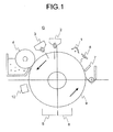
- Fig. 1 is a schematic diagram showing main units of an image forming apparatus according to an embodiment of the present invention.
- the image forming apparatus G includes, as shown in Fig. 1 , a photosensitive drum 9 which is a photosensitive element formed in a drum shape and a rotation driving device (not shown) that rotates the photosensitive drum 9 around an axis line at a predetermined speed.
- the image forming apparatus G includes an electrostatic charger 1, a first print head 2, a second print head 3, a developing device 4, a density sensor 10 which is the density detection unit, a transfer charger 5, a separation charger 6, a cleaning unit 7, and a neutralizing lamp 8, all of which are sequentially arranged in a rotation direction of the photosensitive drum 9 (sub scanning direction: see an arrow) to surround the photosensitive drum 9.
- the separation charger 6 separates transfer paper from the photosensitive drum 9.
- the cleaning unit 7 cleans up a toner remaining on a surface of the photosensitive drum 9 after transfer.
- the neutralizing lamp 8 neutralizes potential remaining on the photosensitive drum 9 after cleaning so as to uniformly eliminate the potential.
- the density sensor 10 is a sensor used to measure (detect) density (toner density) of an image formed on the photosensitive drum 9, such as a reflection type photo sensor, and is used when density of a test pattern image formed on the photosensitive drum 9 is detected in order to determine number of overlap pixels of the first and second print heads 2 and 3, as described below.
- the first and second print heads 2 and 3 are arranged along a width direction (main scanning direction) of the photosensitive drum 9 and are arranged at a predetermined interval in a rotation direction (sub scanning direction) of the photosensitive drum 9.
- the first and second print heads 2 and 3 are arranged in different ranges of the main scanning direction, those ranges being set to the photosensitive drum 9, and ends of the first and second print heads 2 and 3 overlap with each other in the main scanning direction at a boundary between the arrangement ranges thereof such that the arrangement ranges partially overlap each other.
- the first and second print heads 2 and 3 are arranged in the ranges obtained by dividing the photosensitive drum 9 in the width direction while overlapping at a joint of the first and second print heads 2 and 3 (boundary between the arrangement ranges) along the main scanning direction of the photosensitive drum 9.
- Combination of the first and second print heads 2 and 3 is arranged over an entire photosensitive range of the main scanning direction of the photosensitive drum 9 while overlapping parts (ends) thereof in the main scanning direction.
- the first and second print heads 2 and 3 include a plurality of light emitting elements one-dimensionally arranged to form an array (a line) of the light emitting elements.
- the first and second print heads 2 and 3 are each composed of an LED print head including LEDs as the light emitting elements are included.
- the first and second print heads 2 and 3 irradiate light generated when the light emitting element is turned on onto the photosensitive drum 9 so as to form an electrostatic latent image on the surface of the photosensitive drum 9.
- the image forming apparatus G performs divisional exposure, in which two areas obtained by dividing the surface of the photosensitive drum 9 in the main scanning direction are each exposed by one of the first and second print heads 2 and 3, by the first and second print heads 2 and 3 and combines parts of electrostatic latent image each formed on one of the two areas in the main scanning directions so as to form one electrostatic latent image and then develops the electrostatic latent image using a toner of the developing device 4.
- Fig. 2 is a block diagram showing the schematic configuration of the image forming apparatus G and Fig. 3 is a block diagram showing the internal configuration of a control device included in the image forming apparatus G.
- a print head is denoted by LPH in the figure.
- the image forming apparatus G includes, as shown in Fig. 2 , a reading unit 100 that reads an original, an image processing unit 200 that performs image processing on an image (image information) obtained by reading the original, and a writing unit 500 that writes an image when the original is duplicated.
- the image forming apparatus G includes a control device 300 that controls the overall apparatus, and an operation unit 400 with which key input to the control device 300, etc. is performed.
- the abovementioned density sensor 10 is connected to the control device 300.
- the control device 300 includes, as shown in Fig. 3 , a computer including a Central Processing Unit (CPU) 301 configured to execute various arithmetic processing, a Read Only Memory (ROM) 302 that stores various setting information, programs, data, etc. used by the CPU 301, and a Random Access Memory (RAM) 303 that temporarily stores data directly accessed by the CPU 301.
- CPU Central Processing Unit
- ROM Read Only Memory
- RAM Random Access Memory
- the writing unit 500 converts an image data signal transmitted from the image processing unit 200 into bits each corresponding to one pixel using a print head control circuit 501, converts the bits into light (here, infrared light) using the first and second print heads 2 and 3 to output the light.
- the print head control circuit 501 divides an image in a direction corresponding to the width direction of the photosensitive drum 9 and transmits data of the divided images to the first print head 2 and the second print head 3 in parallel with each other.
- the second print head 3 is arranged downstream of the first print head 2 in the rotation direction of the photosensitive drum 9.
- the print head control circuit 501 delays transmission of data to the second print head 3 by a delay time determined by an interval between the first print head 2 and the second print head 3 in the sub scanning direction and a circumferential velocity of the photosensitive drum 9 through a delay circuit. Thereby, an image written by the second print head 3 is synthesized with an image written by the first print head 2 to form a synthesized image along one line on the photosensitive drum 9.
- the image forming apparatus G if the positions of the print heads in the main scanning direction are deviated due to assembling precision or physical dispersion of the first and second print heads 2 and 3, the number of overlap pixels is increased or decreased from a predetermined number and a joint position may be deviated from an expected position (theoretical position) and thus the images may overlap each other in the main scanning direction or, conversely, the images may be separated.
- overlap portions 21 and 31 of the ends of the first and second print heads 2 and 3 are driven by test pattern data so as to form a test pattern image 11, used to detect the number of overlap pixels, on the photosensitive drum 9, density of the test pattern image 11 is detected by the density sensor 10 so as to determine the number N of overlap pixels, and the joint position of the first and second print heads 2 and 3 are determined using a result of determination of the number N.
- the test pattern image 11 is formed only in the overlap portions in order to suppress toner consumption in Fig. 4
- the test pattern image 11 may be formed in a range wider than the overlap portions, for example, in a whole of the first and second print heads 2 and 3 in the main scanning direction.
- a detection range of the density sensor 10 is set to only the overlap portions.
- a method (algorithm) of detecting the number N of overlap pixels will be described.
- a detection example of a case where the number of overlap pixels is 100 will be described. Even when theoretical number of overlap pixels is set to 100, if a deviation of about ⁇ 0.2 mm occurs due to attachment precision error, etc., it is expected that a deviation of about ⁇ 5 pixels (in 600 dpi) may occur and the number of overlap pixels ranges approximately between 95 to 105 pixels. In the present example, it is assumed that a range of deviation is less than or equal to the above value. In the present embodiment, it is assumed that the positions of the dots of the first and second print heads 2 and 3 are aligned by a known dot position misalignment correcting method which is not described in the present embodiment.
- Figs. 5A to 9 are diagrams showing different test pattern images formed on the photosensitive drum 9 and outputs obtained by detecting those test pattern images using the density sensor 10 in the case where the number of overlap pixels is 100. Hereinafter, these will be sequentially described.
- Fig. 5A shows a first test pattern image and Fig. 5B shows an output obtained by detecting that test pattern image using the density sensor 10.
- 100 pixels (overlap pixels) of the overlap portion 21 of the first print head 2 are sequentially denoted by reference numerals "n” to "n-99" from a right end and 100 pixels (overlap pixels) of the overlap portion 31 of the second print head 3 are sequentially denoted by reference numerals "1" to "100” from a left end.
- Test pattern data changing at intervals of 10 dots is written in the overlap pixels of the first print head 2 from an n-th pixel. That is, 10 turned on dots and 10 turned off dots are alternately repeated from the right end.
- Test pattern data changing at intervals of 10 dots is written in the overlap pixels of the second print head 3 from a first pixel. That is, 10 turned on dots and 10 turned off dots are alternately repeated from the left end.
- a black dot denotes the turned on dot and a white dot denotes the turned off dot.
- a test pattern image (first test pattern image) 11_1 formed by developing a latent image of the test pattern formed on the photosensitive drum 9 by both the first print head 2 and the second print head 3 becomes a black solid image.
- an output value of the density sensor 10 at this time becomes a value Vmin.
- This output value Vmin is stored in the RAM 303, etc. Since an amount of reflected light becomes a maximum when the density sensor 10 detects a portion of the photosensitive drum 9, to which a toner is not attached, the output value (drum surface density of Fig. 5B ) of the density sensor 10 at this time is a maximum value.
- a second test pattern image 11_2 is formed on the photosensitive drum 9 by writing second test pattern data onto the first print head 2 and the second print head 3.
- the second test pattern data includes data written onto the first print head 2 that is the same as the first test pattern data, and data written onto the second print head 3 that is obtained by right (in a direction toward a terminal end of main scanning) shifting corresponding data in the first test pattern data by one pixel.
- the second test pattern image 11_2 becomes an image having a portion 11_2a having a width of one dot to which the toner is not attached and, as shown in Fig. 6B , an output value of the density sensor 10 at this time becomes Va (Va > Vmin).
- the output value Va of the density sensor at this time is stored in the RAM 303, etc.
- a third test pattern image 11_3 is formed on the photosensitive drum 9 by writing third test pattern data onto the first print head 2 and the second print head 3.
- the third test pattern data includes data written onto the first print head 2 that is the same as the first test pattern data, and data written onto the second print head 3 that is obtained by right shifting the corresponding data in the first test pattern data by two pixels.
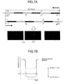
- the third test pattern image 11_3 becomes an image having a portion 11_3a having a width of two dots to which the toner is not attached and, as shown in Fig. 7B , an output value of the density sensor at this time becomes Vb (Vb > Va).
- fourth to eleventh test pattern data are sequentially written onto the first print head 2 and the second print head 3 so as to form fourth to eleventh test pattern images on the photosensitive drum 9.
- the fourth to eleventh test pattern data include data written onto the first print head 2 that is the same as the first test pattern data, and data written onto the second print head 3 that is obtained by right shifting the corresponding data in the first test pattern data by 3 to 10 pixels, respectively.
- Fig. 8A shows an eleventh test pattern image 11_11.
- the eleventh test pattern image 11_11 becomes a lowest-density image having a portion 11_11a having a width of 10 dots to which the toner is not attached and, as shown in Fig. 8B , an output value of the density sensor 10 at this time becomes a maximum value Vmax.
- Output values when the fourth to eleventh test pattern images 11 to 11_11 are detected by the density sensor 10 are stored in the RAM 303, etc.
- Fig. 10A 99 pixels (overlap pixels) of the overlap portion 21 of the first print head 2 are sequentially denoted by reference numerals "n” to "n-98" from the right end and 99 pixels (overlap pixels) of the overlap portion 31 of the second print head 3 are sequentially denoted by reference numerals "1" to "99” from the left end.
- Test pattern data changing at intervals of 10 dots is written in the overlap portion 21 of the first print head 2 from an n-th pixel. That is, 10 turned on dots and 10 turned off dots are alternately repeated from the right end.
- Test pattern data changing at intervals of 10 dots is written in the overlap portion 31 of the second print head 3 from a first pixel. That is, 10 turned on dots and 10 turned off dots are alternately repeated from the left end.
- a black dot denotes the turned on dot and a white dot denotes the turned off dot.
- a test pattern image (first test pattern image) 12_1 formed by developing a latent image of the test pattern formed on the photosensitive drum 9 by both the first print head 2 and the second print head 3 becomes an image having a portion 12_1a having a width of one dot to which the toner is not attached.
- an output value of the density sensor 10 at this time becomes a value Va.
- the output value Va of the density sensor at this time is stored in the RAM 303, etc.
- a second test pattern image 12_2 is formed on the photosensitive drum 9 by writing second test pattern data onto the first print head 2 and the second print head 3.
- the second test pattern data includes data written onto the first print head 2 that is the same as the first test pattern data, and data written onto the second print head 3 that is obtained by right shifting corresponding data in the first test pattern data by one pixel.
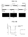
- the second test pattern image 12_2 becomes an image having a portion 12_2a having a width of two dots to which the toner is not attached and, as shown in Fig. 11B , an output value of the density sensor at this time becomes Vb (Vb > Va). This output value Vb of the density sensor at this time is stored in the RAM 303, etc.
- third to eleventh test pattern data are sequentially written onto the first print head 2 and the second print head 3 so as to form third to eleventh test pattern images on the photosensitive drum 9.
- the third to eleventh test pattern data includes data written onto the first print head 2 that is the same as the first test pattern data, and data written onto the second print head 3 that is obtained by right shifting corresponding data in the first test pattern data by 2 to 10 pixels, respectively.
- Fig. 12A shows an eleventh test pattern image 12_11.
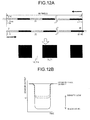
- the images formed by the first print head 2 and the second print head 3 overlap each other so that the eleventh test pattern image 12_11 has a portion 12_11a having a width of 9 dots to which the toner is not attached.
- An output value of the density sensor at this time becomes a value Vi (Vi > Vb).
- the output values when the third to eleventh test pattern images 12_3 to 12_11 are detected by the density sensor 10 are stored in the RAM 303, etc.
- Fig. 14 Some of patterns of the change of the outputs of the density sensor 10 of Table 3 are shown in Fig. 14 .
- the patterns of the change of the outputs when the number of overlap pixels is 95 to 105 are sequentially shown from the left side of the figure.
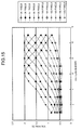
- Fig. 15 is a graph showing a relation between the first to eleventh test pattern images when the number of overlap pixels is 95 to 105 and the outputs detected by the density sensor in Table 3.
- step S1 the photosensitive drum 9 is rotated, the density of the photosensitive drum 9 is read by the density sensor 10, and Vsg adjustment (calibration) is executed.
- n-th test pattern data is written onto the first print head 2 and the second print head 3.
- the first test pattern data is written, that is, data in which 10 turned on dots are repeated at intervals of 10 dots from the right end of the overlap portion 21 is written onto the first print head 2 and data in which 10 turned on dots are repeated at intervals of 10 dots from the left end of the overlap portion 31 is written onto the second print head 3.
- a latent image of the first test pattern is formed on the photosensitive drum 9.
- This latent image is developed by the developing device 4 so that the first test pattern image is formed on the photosensitive drum 9.
- step S4 image density of the n-th test pattern is measured by the density sensor 10 and is stored in the RAM 303.
- step S5 it is determined whether or not all predetermined test pattern data (here, first to eleventh test pattern data) are written onto the first print head 2 and the second print head 3.
- step S5 When it is determined that all data are not written (No in step S5), the pattern number n is incremented by 1 (step S8) and process returns to step S3. In contrast, if the writing up to the eleventh test pattern data is finished (Yes in step S5), the process proceeds to step S6.
- step S6 the density data of each test pattern image stored in the RAM 303 is read, this data is compared by the CPU 301, and the number of overlap pixels is determined from a result of checking transition of change in the data.
- the joint position is determined depending on the number of overlap pixels determined in step S6. That is, for example, if the number of overlap pixels is 100, a joint pixel of the first print head 2 is set to an "n-50"th pixel and a joint pixel of the second print head 3 is set to a 51st pixel.
- the image forming apparatus of the present embodiment it is possible to easily adjust the joint position even in market after shipment by mounting simple and cheap unit (density sensor 10, a program for executing the procedure shown in Fig. 16 , etc.) in a main body of the apparatus.
- the overlap portion may be configured to be wider than the detection range of the density sensor 10 (the detection range of the density sensor 10 may be narrower than the overlap portion). Thereby, it is possible to read the density of the test pattern image in the overlap portion without influence of an attachment error of the density sensor 10.
- test pattern image formed on the photosensitive drum 9 is made thicker by development with the toner, it is preferable to adjust a line width of the test pattern image by adjusting (suppressing) an amount of light of the first print head 2 and the second print head 3, thereby improving output characteristics of the density sensor 10.
- the above-described embodiment relates to an image forming apparatus for performing the divisional exposure in the main scanning direction by two print heads, even in an image forming apparatus that performs the divisional exposure in the main scanning direction by three or more print heads, the joint position of each overlap portion in each two adjacent print heads among the three or more print heads can be adjusted by sequentially or simultaneously executing the procedure shown in Fig. 16 for the each two adjacent print heads.
- the joint position may be roughly determined by shifting data in units of plural pixels and data may be then shifted one pixel by one pixel. Thereby, it is possible to reduce a wasteful toner amount, for example, in a case where a wasteful toner amount becomes large when shifting data one pixel by one pixel since the variation is large.
- an image forming apparatus including an optical writer in which the positions of a plurality of light emitting element array units are different in the sub scanning direction, ends of the light emitting element array units overlap each other in the main scanning direction and the light emitting elements in the ends are used as joints, it is possible to easily adjust the joint position even in the market after shipment by mounting a simple and cheap unit in a main body of the image forming apparatus.
Landscapes
- Physics & Mathematics (AREA)
- Engineering & Computer Science (AREA)
- Microelectronics & Electronic Packaging (AREA)
- General Physics & Mathematics (AREA)
- Optics & Photonics (AREA)
- Health & Medical Sciences (AREA)
- General Health & Medical Sciences (AREA)
- Toxicology (AREA)
- Printers Or Recording Devices Using Electromagnetic And Radiation Means (AREA)
- Facsimile Heads (AREA)
- Control Or Security For Electrophotography (AREA)
- Exposure Or Original Feeding In Electrophotography (AREA)
Abstract
Description
- The present application claims priority to and incorporates by reference the entire contents of Japanese Patent Application No.
2010-207230 - The present invention relates to an image forming apparatus, and a program for the image forming apparatus.
- In an image forming apparatus such as a wide format copier or a wide format printer using electrophotography, there is used an inexpensive light-emitting element array unit having a width of A3 or A4 size, for example, an optical writer having a plurality of light-emitting diode print heads, in which a light emitting diode (LED) serves as a light-emitting element and which are arranged in a main-scanning direction, to performs divisional exposure to thereby deal with wide-format writing.
- In that optical writer, LED print heads adjacent to each other in a main scanning direction are located at different positions in a sub scanning direction and are arranged such that ends of the LED print heads overlap each other in the main scanning direction, and predetermined light emitting elements disposed at the ends of the LED print heads are used as joints, so that images formed by the LED print heads are combined to each other in the main scanning direction.
- For example, if a first LED print head and a second LED print head are arranged to be adjacent to each other in this order from a start end of the main scanning direction, and 10 pixels of each LED print head overlap; for example, a fifth pixel from the start end in the main scanning direction among overlap pixels of the first LED print head and a sixth pixel from the start end in the main scanning direction among overlap pixels of the second LED print head are used as joints to combine the images.
- Accordingly, if misalignment occurs in a positional relationship between adjacent LED print heads due to poor assembling precision of the LED print heads or physical dispersion, number of pixels that overlap may vary, which results in an actual joint position differing from an expected position (theoretical position), hence leading to the images overlapping in the main scanning direction or, conversely being separated.
- As an apparatus intended to solve this problem, there is known a light emitting element array position detection device capable of adjusting a joint position in a manner such that a light-receiving element such as a CCD camera detects outputs of light emission of LED print heads arranged in a staggered manner in the main scanning direction, a computer processes the detected outputs to compute deviated amount of the joint position of LED print heads, and a dot lighting position of either one LED print head of the adjacent LED print heads is moved by the deviated amount (see Japanese Patent Application Laid-open No.
2005-88371 - However, in this light emitting element array position detection device, since adjustment is performed by an external device (jig) other than the optical writer, when the joints are shifted with time or due to the replacement of a part of the LED print heads caused by failure after shipment, the joints must be adjusted on the market. Accordingly, the adjustment is difficult and requires great man hours.
- It is an object of the present invention to at least partially solve the problems in the conventional technology.
- According to an aspect of the present invention, there is provided an image forming apparatus including an optical writer in which positions of a plurality of light emitting element array units are different in a sub scanning direction, ends of the light emitting element array units overlap each other in a main scanning direction and the light emitting elements in the ends are used as joints. The image forming apparatus includes: a print head control unit configured to sequentially form latent images of a plurality of test patterns on a photosensitive element by sequentially writing a plurality of test pattern data onto at least the light emitting elements in the ends of the two light emitting element array units adjacent to each other in the main scanning direction; a test pattern image forming unit configured to sequentially form a plurality of test pattern images on the photosensitive element by operating a developing device to develop the latent images of the plurality of test patterns; a density detection unit configured to operate a density sensor so as to detect density of the plurality of test pattern images; a number-of-overlap-pixels determination unit configured to determine number of the light emitting elements overlapping at the ends based on transition of the density in the plurality of test pattern images; and a joint pixel determination unit configured to determine joint pixels of the two light emitting element array units depending on a result of determination of the number-of-overlap-pixels determination unit. The plurality of test pattern data are configured to cause the light emitting elements of one of the two light emitting element array units to operate such that a predetermined number of the turned on light emitting elements and the predetermined number of the turned off light emitting elements are alternately and repeatedly arranged, and cause the light emitting elements of another of the two light emitting element array units to operate such that the predetermined number of the turned on light emitting elements and the predetermined number of the turned off light emitting elements are alternately and repeatedly arranged, and positions of the turned on light emitting elements and the turned off light emitting elements of the another of the two light emitting element array units are sequentially shifted for each of the plurality of test patterns.
- The above and other objects, features, advantages and technical and industrial significance of this invention will be better understood by reading the following detailed description of presently preferred embodiments of the invention, when considered in connection with the accompanying drawings.
-
-
Fig. 1 is a schematic diagram showing main units of an image forming apparatus according to an embodiment of the present invention; -
Fig. 2 is a block diagram showing a schematic configuration of an image forming apparatus according to an embodiment of the present invention; -
Fig. 3 is a block diagram showing an internal configuration of a control device included in an image forming apparatus according to an embodiment of the present invention; -
Fig. 4 is a diagram showing a relation among two print heads adjacent to each other in a main scanning direction, a test pattern formed on a photosensitive drum, and a density sensor in an image forming apparatus according to an embodiment of the present invention; -
Fig. 5A is a diagram showing a first test pattern image formed on a photosensitive drum if number of overlap pixels is 100; -
Fig. 5B is a diagram showing an output obtained by detecting the first test pattern image using the density sensor; -
Fig. 6A is a diagram showing a second test pattern image formed on a photosensitive drum if the number of overlap pixels is 100; -
Fig. 6B is a diagram showing an output obtained by detecting the second test pattern image using the density sensor; -
Fig. 7A is a diagram showing a third test pattern image formed on a photosensitive drum if the number of overlap pixels is 100; - and
Fig. 7B is a diagram showing an output obtained by detecting the third test pattern image using the density sensor; -
Fig. 8A is a diagram showing an eleventh test pattern image formed on a photosensitive drum if the number of overlap pixels is 100; -
Fig. 8B is a diagram showing an output obtained by detecting the eleventh test pattern image using the density sensor; -
Fig. 9 is a diagram showing a relation between the first to eleventh test pattern images and outputs detected by the density sensor if the number of overlap pixels is 100; -
Fig. 10A is a diagram showing the first test pattern image formed on a photosensitive drum if the number of overlap pixels is 99; -
Fig. 10B is a diagram showing an output obtained by detecting the first test pattern image using the density sensor; -
Fig. 11A is a diagram showing the second test pattern image formed on a photosensitive drum if the number of overlap pixels is 99; -
Fig. 11B is a diagram showing an output obtained by detecting the second test pattern image using the density sensor; -
Fig. 12A is a diagram showing the eleventh test pattern image formed on a photosensitive drum if the number of overlap pixels is 99; -
Fig. 12B is a diagram showing an output obtained by detecting the eleventh test pattern image using the density sensor; -
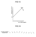
Fig. 13 is a diagram showing a relation between the first to eleventh test pattern images and outputs detected by the density sensor if the number of overlap pixels is 99; -
Fig. 14 is a diagram showing an example of a pattern of an output change of the density sensor as the number of overlap pixels of Table 3 changes from 95 to 105; -
Fig. 15 is a diagram showing a relation between the first to eleventh test pattern images and outputs detected by the density sensor as the number of overlap pixels of table 3 changes from 95 to 105; and -
Fig. 16 is a flowchart illustrating a procedure of determining the number of overlap pixels and performing adjustment of a joint position in an image forming apparatus according to an embodiment of the present invention. -
Fig. 1 is a schematic diagram showing main units of an image forming apparatus according to an embodiment of the present invention. The image forming apparatus G includes, as shown inFig. 1 , aphotosensitive drum 9 which is a photosensitive element formed in a drum shape and a rotation driving device (not shown) that rotates thephotosensitive drum 9 around an axis line at a predetermined speed. The image forming apparatus G includes anelectrostatic charger 1, afirst print head 2, asecond print head 3, a developingdevice 4, adensity sensor 10 which is the density detection unit, atransfer charger 5, aseparation charger 6, acleaning unit 7, and a neutralizinglamp 8, all of which are sequentially arranged in a rotation direction of the photosensitive drum 9 (sub scanning direction: see an arrow) to surround thephotosensitive drum 9. - The
separation charger 6 separates transfer paper from thephotosensitive drum 9. Thecleaning unit 7 cleans up a toner remaining on a surface of thephotosensitive drum 9 after transfer. The neutralizinglamp 8 neutralizes potential remaining on thephotosensitive drum 9 after cleaning so as to uniformly eliminate the potential. Thedensity sensor 10 is a sensor used to measure (detect) density (toner density) of an image formed on thephotosensitive drum 9, such as a reflection type photo sensor, and is used when density of a test pattern image formed on thephotosensitive drum 9 is detected in order to determine number of overlap pixels of the first andsecond print heads - The first and
second print heads photosensitive drum 9 and are arranged at a predetermined interval in a rotation direction (sub scanning direction) of thephotosensitive drum 9. The first andsecond print heads photosensitive drum 9, and ends of the first andsecond print heads second print heads photosensitive drum 9 in the width direction while overlapping at a joint of the first andsecond print heads 2 and 3 (boundary between the arrangement ranges) along the main scanning direction of thephotosensitive drum 9. Combination of the first andsecond print heads photosensitive drum 9 while overlapping parts (ends) thereof in the main scanning direction. - The first and
second print heads second print heads second print heads photosensitive drum 9 so as to form an electrostatic latent image on the surface of thephotosensitive drum 9. At this time, the image forming apparatus G performs divisional exposure, in which two areas obtained by dividing the surface of thephotosensitive drum 9 in the main scanning direction are each exposed by one of the first andsecond print heads second print heads device 4. -
Fig. 2 is a block diagram showing the schematic configuration of the image forming apparatus G andFig. 3 is a block diagram showing the internal configuration of a control device included in the image forming apparatus G. Incidentally, a print head is denoted by LPH in the figure. - The image forming apparatus G includes, as shown in
Fig. 2 , areading unit 100 that reads an original, animage processing unit 200 that performs image processing on an image (image information) obtained by reading the original, and awriting unit 500 that writes an image when the original is duplicated. The image forming apparatus G includes acontrol device 300 that controls the overall apparatus, and anoperation unit 400 with which key input to thecontrol device 300, etc. is performed. Theabovementioned density sensor 10 is connected to thecontrol device 300. - The
control device 300 includes, as shown inFig. 3 , a computer including a Central Processing Unit (CPU) 301 configured to execute various arithmetic processing, a Read Only Memory (ROM) 302 that stores various setting information, programs, data, etc. used by theCPU 301, and a Random Access Memory (RAM) 303 that temporarily stores data directly accessed by theCPU 301. In the present embodiment, each unit of the present invention is realized by executing a program using the computer. - The writing unit 500 (see
Fig. 2 ) converts an image data signal transmitted from theimage processing unit 200 into bits each corresponding to one pixel using a print head control circuit 501, converts the bits into light (here, infrared light) using the first andsecond print heads photosensitive drum 9 and transmits data of the divided images to thefirst print head 2 and thesecond print head 3 in parallel with each other. Thesecond print head 3 is arranged downstream of thefirst print head 2 in the rotation direction of thephotosensitive drum 9. The print head control circuit 501 delays transmission of data to thesecond print head 3 by a delay time determined by an interval between thefirst print head 2 and thesecond print head 3 in the sub scanning direction and a circumferential velocity of thephotosensitive drum 9 through a delay circuit. Thereby, an image written by thesecond print head 3 is synthesized with an image written by thefirst print head 2 to form a synthesized image along one line on thephotosensitive drum 9. - In the image forming apparatus G, if the positions of the print heads in the main scanning direction are deviated due to assembling precision or physical dispersion of the first and
second print heads - If the number of overlap pixels is determined, it is possible to determine the joint position. In the present embodiment, as shown in
Fig. 4 ,overlap portions second print heads test pattern image 11, used to detect the number of overlap pixels, on thephotosensitive drum 9, density of thetest pattern image 11 is detected by thedensity sensor 10 so as to determine the number N of overlap pixels, and the joint position of the first andsecond print heads test pattern image 11 is formed only in the overlap portions in order to suppress toner consumption inFig. 4 , thetest pattern image 11 may be formed in a range wider than the overlap portions, for example, in a whole of the first andsecond print heads density sensor 10 is set to only the overlap portions. - Hereinafter, a method (algorithm) of detecting the number N of overlap pixels will be described. First, a detection example of a case where the number of overlap pixels is 100 will be described. Even when theoretical number of overlap pixels is set to 100, if a deviation of about ±0.2 mm occurs due to attachment precision error, etc., it is expected that a deviation of about ±5 pixels (in 600 dpi) may occur and the number of overlap pixels ranges approximately between 95 to 105 pixels. In the present example, it is assumed that a range of deviation is less than or equal to the above value. In the present embodiment, it is assumed that the positions of the dots of the first and
second print heads -
Figs. 5A to 9 are diagrams showing different test pattern images formed on thephotosensitive drum 9 and outputs obtained by detecting those test pattern images using thedensity sensor 10 in the case where the number of overlap pixels is 100. Hereinafter, these will be sequentially described. - First,
Fig. 5A shows a first test pattern image andFig. 5B shows an output obtained by detecting that test pattern image using thedensity sensor 10. InFig. 5A , 100 pixels (overlap pixels) of theoverlap portion 21 of thefirst print head 2 are sequentially denoted by reference numerals "n" to "n-99" from a right end and 100 pixels (overlap pixels) of theoverlap portion 31 of thesecond print head 3 are sequentially denoted by reference numerals "1" to "100" from a left end. Test pattern data changing at intervals of 10 dots is written in the overlap pixels of thefirst print head 2 from an n-th pixel. That is, 10 turned on dots and 10 turned off dots are alternately repeated from the right end. Test pattern data changing at intervals of 10 dots is written in the overlap pixels of thesecond print head 3 from a first pixel. That is, 10 turned on dots and 10 turned off dots are alternately repeated from the left end. In the figure, a black dot denotes the turned on dot and a white dot denotes the turned off dot. These define the first test pattern data. - At this time, a test pattern image (first test pattern image) 11_1 formed by developing a latent image of the test pattern formed on the
photosensitive drum 9 by both thefirst print head 2 and thesecond print head 3 becomes a black solid image. As shown inFig. 5B , an output value of thedensity sensor 10 at this time becomes a value Vmin. This output value Vmin is stored in theRAM 303, etc. Since an amount of reflected light becomes a maximum when thedensity sensor 10 detects a portion of thephotosensitive drum 9, to which a toner is not attached, the output value (drum surface density ofFig. 5B ) of thedensity sensor 10 at this time is a maximum value. - Next, as shown in
Fig. 6A , a second test pattern image 11_2 is formed on thephotosensitive drum 9 by writing second test pattern data onto thefirst print head 2 and thesecond print head 3. The second test pattern data includes data written onto thefirst print head 2 that is the same as the first test pattern data, and data written onto thesecond print head 3 that is obtained by right (in a direction toward a terminal end of main scanning) shifting corresponding data in the first test pattern data by one pixel. The second test pattern image 11_2 becomes an image having a portion 11_2a having a width of one dot to which the toner is not attached and, as shown inFig. 6B , an output value of thedensity sensor 10 at this time becomes Va (Va > Vmin). The output value Va of the density sensor at this time is stored in theRAM 303, etc. - Next, as shown in
Fig. 7A , a third test pattern image 11_3 is formed on thephotosensitive drum 9 by writing third test pattern data onto thefirst print head 2 and thesecond print head 3. The third test pattern data includes data written onto thefirst print head 2 that is the same as the first test pattern data, and data written onto thesecond print head 3 that is obtained by right shifting the corresponding data in the first test pattern data by two pixels. The third test pattern image 11_3 becomes an image having a portion 11_3a having a width of two dots to which the toner is not attached and, as shown inFig. 7B , an output value of the density sensor at this time becomes Vb (Vb > Va). - Thereafter, fourth to eleventh test pattern data are sequentially written onto the
first print head 2 and thesecond print head 3 so as to form fourth to eleventh test pattern images on thephotosensitive drum 9. The fourth to eleventh test pattern data include data written onto thefirst print head 2 that is the same as the first test pattern data, and data written onto thesecond print head 3 that is obtained by right shifting the corresponding data in the first test pattern data by 3 to 10 pixels, respectively.Fig. 8A shows an eleventh test pattern image 11_11. The eleventh test pattern image 11_11 becomes a lowest-density image having a portion 11_11a having a width of 10 dots to which the toner is not attached and, as shown inFig. 8B , an output value of thedensity sensor 10 at this time becomes a maximum value Vmax. Output values when the fourth to eleventhtest pattern images 11 to 11_11 are detected by thedensity sensor 10 are stored in theRAM 303, etc. - As described above, the outputs of the density sensor when the test pattern data written onto the
second print head 3 are sequentially changed are shown in Table 1 below. In this table, "Vmin < Va < Vb < Vc < Vd < Ve < Vf < Vg < Vh < Vi < Vmax" is satisfied.Table 1 Pattern number Output value of density sensor 1 Vmin 2 Va 3 Vb 4 Vc 5 Vd 6 Ve 7 Vf 8 Vg 9 Vh 10 Vi 11 Vmax - It can be seen from this table that, in the case where the number N of overlap pixels is 100, the outputs of the density sensor constantly increases from Vmin to Vmax as the test pattern data written onto the
second print head 3 are sequentially right shifted by 1 to 10 pixels, as shown inFig. 9 . - Next, different test pattern images formed on the
photosensitive drum 9 and outputs obtained by detecting the test pattern images using thedensity sensor 10 in a case where the number N of overlap pixels is 99 will be described. - In
Fig. 10A , 99 pixels (overlap pixels) of theoverlap portion 21 of thefirst print head 2 are sequentially denoted by reference numerals "n" to "n-98" from the right end and 99 pixels (overlap pixels) of theoverlap portion 31 of thesecond print head 3 are sequentially denoted by reference numerals "1" to "99" from the left end. Test pattern data changing at intervals of 10 dots is written in theoverlap portion 21 of thefirst print head 2 from an n-th pixel. That is, 10 turned on dots and 10 turned off dots are alternately repeated from the right end. Test pattern data changing at intervals of 10 dots is written in theoverlap portion 31 of thesecond print head 3 from a first pixel. That is, 10 turned on dots and 10 turned off dots are alternately repeated from the left end. In the figure, a black dot denotes the turned on dot and a white dot denotes the turned off dot. These define the first test pattern data. - At this time, a test pattern image (first test pattern image) 12_1 formed by developing a latent image of the test pattern formed on the
photosensitive drum 9 by both thefirst print head 2 and thesecond print head 3 becomes an image having a portion 12_1a having a width of one dot to which the toner is not attached. As shown inFig. 10B , an output value of thedensity sensor 10 at this time becomes a value Va. The output value Va of the density sensor at this time is stored in theRAM 303, etc. - Next, as shown in
Fig. 11A , a second test pattern image 12_2 is formed on thephotosensitive drum 9 by writing second test pattern data onto thefirst print head 2 and thesecond print head 3. The second test pattern data includes data written onto thefirst print head 2 that is the same as the first test pattern data, and data written onto thesecond print head 3 that is obtained by right shifting corresponding data in the first test pattern data by one pixel. The second test pattern image 12_2 becomes an image having a portion 12_2a having a width of two dots to which the toner is not attached and, as shown inFig. 11B , an output value of the density sensor at this time becomes Vb (Vb > Va). This output value Vb of the density sensor at this time is stored in theRAM 303, etc. - Thereafter, third to eleventh test pattern data are sequentially written onto the
first print head 2 and thesecond print head 3 so as to form third to eleventh test pattern images on thephotosensitive drum 9. The third to eleventh test pattern data includes data written onto thefirst print head 2 that is the same as the first test pattern data, and data written onto thesecond print head 3 that is obtained by right shifting corresponding data in the first test pattern data by 2 to 10 pixels, respectively.Fig. 12A shows an eleventh test pattern image 12_11. In the eleventh test pattern image 12_11, the images formed by thefirst print head 2 and thesecond print head 3 overlap each other so that the eleventh test pattern image 12_11 has a portion 12_11a having a width of 9 dots to which the toner is not attached. An output value of the density sensor at this time becomes a value Vi (Vi > Vb). The output values when the third to eleventh test pattern images 12_3 to 12_11 are detected by thedensity sensor 10 are stored in theRAM 303, etc. - As described above, the outputs of the density sensor when the test pattern data written onto the
second print head 3 are sequentially changed are shown in Table 2. In this table, "(Vmin) < Va < Vb < Vc < Vd < Ve < Vf < Vg < Vh < Vi < Vmax" is satisfied.Table 2 Pattern number Output value of density sensor 1 Va 2 Vb 3 Vc 4 Vd 5 Ve 6 Vf 7 Vg 8 Vh 9 Vi 10 Vmax 11 Vi - It can be seen from this table that, in the case where the number N of overlap pixels is 99, the outputs of the density sensor constantly increase from Va to Vmax and then decrease to Vi as the test pattern data written onto the
second print head 3 are sequentially right shifted by 1 to 10 pixels, as shown inFig. 13 . - With respect to the number of overlap pixels of 90 to 98 and 101 to 110, data shown in Table 3 can be obtained by forming first to eleventh test pattern images and detecting the density thereof by the
density sensor 10.

- It can be seen from Table 3 that, since change of the outputs of the
density sensor 10 is different depending on the number of overlap pixels, it is possible to determine the number of overlap pixels by checking how the outputs of thedensity sensor 10 are changed. That is, for example, when the outputs of thedensity sensor 10 change form Vmin to Vmax, it is determined that the number of overlap pixels is 100. - In a case of the test pattern data changing at intervals of a pattern width of 10 dots, since change of the outputs of the
density sensor 10 in a case where the number of overlap pixels is a value equal to or less than 90 or equal to or greater than 110 is identical to that in a case where the number of overlap pixels is different from that value, it is possible to detect change of the number of overlap pixels up to ±9 dots. If a variation of the number of overlap pixels is larger or smaller, it is possible to change a detectable change of the number of overlap pixels by changing the pattern width. - Some of patterns of the change of the outputs of the
density sensor 10 of Table 3 are shown inFig. 14 . The patterns of the change of the outputs when the number of overlap pixels is 95 to 105 are sequentially shown from the left side of the figure.Fig. 15 is a graph showing a relation between the first to eleventh test pattern images when the number of overlap pixels is 95 to 105 and the outputs detected by the density sensor in Table 3. - The process of determining the number of overlap pixels by the above-described procedure and performing adjustment of the joint position using a result of the determining will be described using the flowchart shown in
Fig. 16 . - In step S1, the
photosensitive drum 9 is rotated, the density of thephotosensitive drum 9 is read by thedensity sensor 10, and Vsg adjustment (calibration) is executed. - In step S2, a pattern number n of the test pattern data to be output to the
first print head 2 and thesecond print head 3 is initialized (n = 1). - In step S3, n-th test pattern data is written onto the
first print head 2 and thesecond print head 3. Here, since n = 1, the first test pattern data is written, that is, data in which 10 turned on dots are repeated at intervals of 10 dots from the right end of theoverlap portion 21 is written onto thefirst print head 2 and data in which 10 turned on dots are repeated at intervals of 10 dots from the left end of theoverlap portion 31 is written onto thesecond print head 3. Thus, a latent image of the first test pattern is formed on thephotosensitive drum 9. This latent image is developed by the developingdevice 4 so that the first test pattern image is formed on thephotosensitive drum 9. - In step S4, image density of the n-th test pattern is measured by the
density sensor 10 and is stored in theRAM 303. - In step S5, it is determined whether or not all predetermined test pattern data (here, first to eleventh test pattern data) are written onto the
first print head 2 and thesecond print head 3. - When it is determined that all data are not written (No in step S5), the pattern number n is incremented by 1 (step S8) and process returns to step S3. In contrast, if the writing up to the eleventh test pattern data is finished (Yes in step S5), the process proceeds to step S6.
- In step S6, the density data of each test pattern image stored in the
RAM 303 is read, this data is compared by theCPU 301, and the number of overlap pixels is determined from a result of checking transition of change in the data. - In last step S7, the joint position is determined depending on the number of overlap pixels determined in step S6. That is, for example, if the number of overlap pixels is 100, a joint pixel of the
first print head 2 is set to an "n-50"th pixel and a joint pixel of thesecond print head 3 is set to a 51st pixel. - As described in detail above, according to the image forming apparatus of the present embodiment, it is possible to easily adjust the joint position even in market after shipment by mounting simple and cheap unit (
density sensor 10, a program for executing the procedure shown inFig. 16 , etc.) in a main body of the apparatus. - Although a detection range of the
density sensor 10 in the main scanning direction is set to the overlap portion in the above-described embodiment, the overlap portion may be configured to be wider than the detection range of the density sensor 10 (the detection range of thedensity sensor 10 may be narrower than the overlap portion). Thereby, it is possible to read the density of the test pattern image in the overlap portion without influence of an attachment error of thedensity sensor 10. - Since the test pattern image formed on the
photosensitive drum 9 is made thicker by development with the toner, it is preferable to adjust a line width of the test pattern image by adjusting (suppressing) an amount of light of thefirst print head 2 and thesecond print head 3, thereby improving output characteristics of thedensity sensor 10. - Although the above-described embodiment relates to an image forming apparatus for performing the divisional exposure in the main scanning direction by two print heads, even in an image forming apparatus that performs the divisional exposure in the main scanning direction by three or more print heads, the joint position of each overlap portion in each two adjacent print heads among the three or more print heads can be adjusted by sequentially or simultaneously executing the procedure shown in
Fig. 16 for the each two adjacent print heads. - Although data written onto the
second print head 3 is sequentially right shifted one pixel by one pixel in the above-described embodiment, the joint position may be roughly determined by shifting data in units of plural pixels and data may be then shifted one pixel by one pixel. Thereby, it is possible to reduce a wasteful toner amount, for example, in a case where a wasteful toner amount becomes large when shifting data one pixel by one pixel since the variation is large. - According to the present invention, in an image forming apparatus including an optical writer in which the positions of a plurality of light emitting element array units are different in the sub scanning direction, ends of the light emitting element array units overlap each other in the main scanning direction and the light emitting elements in the ends are used as joints, it is possible to easily adjust the joint position even in the market after shipment by mounting a simple and cheap unit in a main body of the image forming apparatus.
- Although the invention has been described with respect to specific embodiments for a complete and clear disclosure, the appended claims are not to be thus limited but are to be construed as embodying all modifications and alternative constructions that may occur to one skilled in the art that fairly fall within the basic teaching herein set forth.
Claims (7)
- An image forming apparatus (G) including an optical writer (500) in which positions of a plurality of light emitting element array units (2, 3) are different in a sub scanning direction, ends of the light emitting element array units overlap each other in a main scanning direction and the light emitting elements in the ends are used as joints, the image forming apparatus comprising:a print head control unit (501) configured to sequentially form latent images of a plurality of test patterns on a photosensitive element (9) by sequentially writing a plurality of test pattern data onto at least the light emitting elements in the ends of the two light emitting element array units adjacent to each other in the main scanning direction;a test pattern image forming unit (300) configured to sequentially form a plurality of test pattern images on the photosensitive element by operating a developing device (4) to develop the latent images of the plurality of test patterns;a density detection unit (300) configured to operate a density sensor (10) so as to detect density of the plurality of test pattern images;a number-of-overlap-pixels determination unit (300) configured to determine number of the light emitting elements overlapping at the ends based on transition of the density in the plurality of test pattern images; anda joint pixel determination unit (300) configured to determine joint pixels of the two light emitting element array units depending on a result of determination of the number-of-overlap-pixels determination unit,wherein the plurality of test pattern data are configured to cause the light emitting elements of one of the two light emitting element array units to operate such that a predetermined number of the turned on light emitting elements and the predetermined number of the turned off light emitting elements are alternately and repeatedly arranged, and cause the light emitting elements of another of the two light emitting element array units to operate such that the predetermined number of the turned on light emitting elements and the predetermined number of the turned off light emitting elements are alternately and repeatedly arranged, and positions of the turned on light emitting elements and the turned off light emitting elements of the another of the two light emitting element array units are sequentially shifted for each of the plurality of test patterns.
- The image forming apparatus (G) according to claim 1, further comprising a unit (300) configured to change the predetermined number.
- The image forming apparatus (G) according to claim 1 or 2, further comprising a unit (300) configured to adjust an amount of light of the light emitting elements.
- The image forming apparatus (G) according to any one of claims 1 to 3, wherein length of overlap portions of the ends in the main scanning direction is greater than length of a detection range of the density sensor (10) in the main scanning direction.
- The image forming apparatus (G) according to any one of claims 1 to 4, wherein the print head control unit (501) writes the plurality of test pattern data only onto the light emitting elements in the ends of the two light emitting element array units (2, 3).
- The image forming apparatus (G) according to any one of claims 1 to 5, wherein the positions of the turned on light emitting elements and the turned off light emitting elements of the another of the two light emitting element array units are sequentially shifted by one pixel for each of the plurality of test patterns.
- A computer program product comprising a non-transitory computer-usable medium having computer-readable program codes embodied in the medium, wherein the program codes when executed causing a computer (300, 500) to function as the units of the image forming apparatus according to any one of claims 1 to 6.
Applications Claiming Priority (1)
| Application Number | Priority Date | Filing Date | Title |
|---|---|---|---|
| JP2010207230A JP5740880B2 (en) | 2010-09-15 | 2010-09-15 | Image forming apparatus and program |
Publications (3)
| Publication Number | Publication Date |
|---|---|
| EP2444850A2 true EP2444850A2 (en) | 2012-04-25 |
| EP2444850A3 EP2444850A3 (en) | 2017-06-14 |
| EP2444850B1 EP2444850B1 (en) | 2018-11-07 |
Family
ID=44905384
Family Applications (1)
| Application Number | Title | Priority Date | Filing Date |
|---|---|---|---|
| EP11181321.8A Not-in-force EP2444850B1 (en) | 2010-09-15 | 2011-09-15 | Image forming apparatus and program |
Country Status (2)
| Country | Link |
|---|---|
| EP (1) | EP2444850B1 (en) |
| JP (1) | JP5740880B2 (en) |
Cited By (3)
| Publication number | Priority date | Publication date | Assignee | Title |
|---|---|---|---|---|
| DE102014203420A1 (en) * | 2014-02-26 | 2015-08-27 | Koenig & Bauer Aktiengesellschaft | Method for adjusting relative printhead settings and a printing unit |
| US9836674B2 (en) * | 2015-12-18 | 2017-12-05 | Fuji Xerox Co., Ltd. | Control device forming a plurality of latent images based on one input image by using a light source including a plurality of light emitting members, and control method, image forming apparatus, and non-transitory computer readable medium thereof |
| EP3657262A1 (en) * | 2018-11-22 | 2020-05-27 | Canon Kabushiki Kaisha | Image forming apparatus |
Families Citing this family (3)
| Publication number | Priority date | Publication date | Assignee | Title |
|---|---|---|---|---|
| JP5928384B2 (en) * | 2013-03-22 | 2016-06-01 | 富士ゼロックス株式会社 | Light emitting element head and method for manufacturing light emitting element head |
| KR102198052B1 (en) * | 2015-11-16 | 2021-01-04 | 휴렛-팩커드 디벨롭먼트 컴퍼니, 엘.피. | Image forming apparatus and controlling method thereof |
| CN116156342B (en) * | 2023-04-04 | 2023-06-27 | 合肥埃科光电科技股份有限公司 | Multi-linear array image sensor splicing method, linear array image acquisition system and device |
Citations (2)
| Publication number | Priority date | Publication date | Assignee | Title |
|---|---|---|---|---|
| JP2005088371A (en) | 2003-09-17 | 2005-04-07 | Ricoh Co Ltd | Light emitting device array position detection device |
| JP2010207230A (en) | 2002-12-06 | 2010-09-24 | Millennium Pharmaceuticals Inc | Method for identification, assessment, and treatment of patient with proteasome inhibition therapy |
Family Cites Families (5)
| Publication number | Priority date | Publication date | Assignee | Title |
|---|---|---|---|---|
| JP3287289B2 (en) * | 1997-11-18 | 2002-06-04 | 富士ゼロックス株式会社 | Image forming apparatus and control method of divided optical scanning device |
| JP3542720B2 (en) * | 1998-09-07 | 2004-07-14 | シャープ株式会社 | Image forming device |
| JP3708006B2 (en) * | 1999-08-20 | 2005-10-19 | 株式会社沖データ | Image recording device |
| JP4019654B2 (en) * | 2000-05-29 | 2007-12-12 | 富士ゼロックス株式会社 | Image forming apparatus |
| JP2005031227A (en) * | 2003-07-09 | 2005-02-03 | Ricoh Co Ltd | Method for forming misregistration correction pattern, misregistration correction device, image forming apparatus, misregistration correction method, computer program, and recording medium |
-
2010
- 2010-09-15 JP JP2010207230A patent/JP5740880B2/en not_active Expired - Fee Related
-
2011
- 2011-09-15 EP EP11181321.8A patent/EP2444850B1/en not_active Not-in-force
Patent Citations (2)
| Publication number | Priority date | Publication date | Assignee | Title |
|---|---|---|---|---|
| JP2010207230A (en) | 2002-12-06 | 2010-09-24 | Millennium Pharmaceuticals Inc | Method for identification, assessment, and treatment of patient with proteasome inhibition therapy |
| JP2005088371A (en) | 2003-09-17 | 2005-04-07 | Ricoh Co Ltd | Light emitting device array position detection device |
Cited By (6)
| Publication number | Priority date | Publication date | Assignee | Title |
|---|---|---|---|---|
| DE102014203420A1 (en) * | 2014-02-26 | 2015-08-27 | Koenig & Bauer Aktiengesellschaft | Method for adjusting relative printhead settings and a printing unit |
| US9604450B2 (en) | 2014-02-26 | 2017-03-28 | Koenig & Bauer Ag | Method for adapting relative settings of printing heads, and printing machine |
| US9836674B2 (en) * | 2015-12-18 | 2017-12-05 | Fuji Xerox Co., Ltd. | Control device forming a plurality of latent images based on one input image by using a light source including a plurality of light emitting members, and control method, image forming apparatus, and non-transitory computer readable medium thereof |
| EP3657262A1 (en) * | 2018-11-22 | 2020-05-27 | Canon Kabushiki Kaisha | Image forming apparatus |
| CN111208719A (en) * | 2018-11-22 | 2020-05-29 | 佳能株式会社 | Image forming apparatus with a toner supply device |
| US10901338B2 (en) | 2018-11-22 | 2021-01-26 | Canon Kabushiki Kaisha | Image forming apparatus with photosensitive drum exposed by linearly-arranged light emission elements having an overlap |
Also Published As
| Publication number | Publication date |
|---|---|
| JP2012061695A (en) | 2012-03-29 |
| JP5740880B2 (en) | 2015-07-01 |
| EP2444850B1 (en) | 2018-11-07 |
| EP2444850A3 (en) | 2017-06-14 |
Similar Documents
| Publication | Publication Date | Title |
|---|---|---|
| US8294744B2 (en) | Optical writing device, image forming apparatus, method of controlling optical writing device, and computer program product | |
| US8600283B2 (en) | Method of compensating for errors caused by a print head using skew correction | |
| US7663654B2 (en) | Image formation device and method for correcting periodic variations | |
| EP2738617B1 (en) | Optical writing control device, image forming apparatus, and method of controlling optical writing device | |
| EP2444850B1 (en) | Image forming apparatus and program | |
| US7817948B2 (en) | Image forming apparatus and control method of image forming apparatus | |
| US8917303B2 (en) | Optical writing device, image forming device, and method of operating the same | |
| US8581944B2 (en) | Image forming apparatus and method for detecting position deviation | |
| US8723905B2 (en) | Light source control circuit, image forming apparatus, and method of controlling the light source control circuit | |
| US9191540B2 (en) | Image processing device and method of acquiring amount of density deviation of light-emitting-element group | |
| KR20110085892A (en) | Image forming apparatus, control method and storage medium | |
| CN110191249A (en) | Print head and image forming device | |
| US9383675B2 (en) | Image processing device and method of acquiring amount of positional deviation of light-emitting-element array | |
| US20080170892A1 (en) | Auto color registration apparatus and method thereof | |
| JP2006234941A (en) | Image forming apparatus | |
| JP2005274919A (en) | Image forming apparatus | |
| US20150125170A1 (en) | Image forming apparatus | |
| US12360474B2 (en) | Image-forming apparatus and method for suppressing generation of a density level difference caused by reciprocity failure | |
| JP2005233983A (en) | Image forming apparatus and the method | |
| JPH1073980A (en) | Color shift correction method for image forming apparatus | |
| JP4396188B2 (en) | Timing control apparatus and image forming apparatus | |
| KR100602270B1 (en) | Skew Correction Apparatus and Method in Color Image Forming Machine | |
| JPH0766953A (en) | Color misregistration correction device in color electrophotographic apparatus | |
| JP2015197610A (en) | image forming apparatus | |
| JP2000047546A (en) | Image forming device |
Legal Events
| Date | Code | Title | Description |
|---|---|---|---|
| 17P | Request for examination filed |
Effective date: 20110915 |
|
| AK | Designated contracting states |
Kind code of ref document: A2 Designated state(s): AL AT BE BG CH CY CZ DE DK EE ES FI FR GB GR HR HU IE IS IT LI LT LU LV MC MK MT NL NO PL PT RO RS SE SI SK SM TR |
|
| AX | Request for extension of the european patent |
Extension state: BA ME |
|
| PUAI | Public reference made under article 153(3) epc to a published international application that has entered the european phase |
Free format text: ORIGINAL CODE: 0009012 |
|
| PUAL | Search report despatched |
Free format text: ORIGINAL CODE: 0009013 |
|
| AK | Designated contracting states |
Kind code of ref document: A3 Designated state(s): AL AT BE BG CH CY CZ DE DK EE ES FI FR GB GR HR HU IE IS IT LI LT LU LV MC MK MT NL NO PL PT RO RS SE SI SK SM TR |
|
| AX | Request for extension of the european patent |
Extension state: BA ME |
|
| RIC1 | Information provided on ipc code assigned before grant |
Ipc: G03G 15/00 20060101AFI20170505BHEP Ipc: B41J 2/45 20060101ALI20170505BHEP |
|
| GRAP | Despatch of communication of intention to grant a patent |
Free format text: ORIGINAL CODE: EPIDOSNIGR1 |
|
| STAA | Information on the status of an ep patent application or granted ep patent |
Free format text: STATUS: GRANT OF PATENT IS INTENDED |
|
| INTG | Intention to grant announced |
Effective date: 20180528 |
|
| GRAS | Grant fee paid |
Free format text: ORIGINAL CODE: EPIDOSNIGR3 |
|
| GRAA | (expected) grant |
Free format text: ORIGINAL CODE: 0009210 |
|
| STAA | Information on the status of an ep patent application or granted ep patent |
Free format text: STATUS: THE PATENT HAS BEEN GRANTED |
|
| AK | Designated contracting states |
Kind code of ref document: B1 Designated state(s): AL AT BE BG CH CY CZ DE DK EE ES FI FR GB GR HR HU IE IS IT LI LT LU LV MC MK MT NL NO PL PT RO RS SE SI SK SM TR |
|
| REG | Reference to a national code |
Ref country code: GB Ref legal event code: FG4D |
|
| REG | Reference to a national code |
Ref country code: CH Ref legal event code: EP Ref country code: AT Ref legal event code: REF Ref document number: 1062824 Country of ref document: AT Kind code of ref document: T Effective date: 20181115 |
|
| REG | Reference to a national code |
Ref country code: IE Ref legal event code: FG4D |
|
| REG | Reference to a national code |
Ref country code: DE Ref legal event code: R096 Ref document number: 602011053580 Country of ref document: DE |
|
| REG | Reference to a national code |
Ref country code: NL Ref legal event code: MP Effective date: 20181107 |
|
| REG | Reference to a national code |
Ref country code: LT Ref legal event code: MG4D |
|
| REG | Reference to a national code |
Ref country code: AT Ref legal event code: MK05 Ref document number: 1062824 Country of ref document: AT Kind code of ref document: T Effective date: 20181107 |
|
| PG25 | Lapsed in a contracting state [announced via postgrant information from national office to epo] |
Ref country code: LV Free format text: LAPSE BECAUSE OF FAILURE TO SUBMIT A TRANSLATION OF THE DESCRIPTION OR TO PAY THE FEE WITHIN THE PRESCRIBED TIME-LIMIT Effective date: 20181107 Ref country code: HR Free format text: LAPSE BECAUSE OF FAILURE TO SUBMIT A TRANSLATION OF THE DESCRIPTION OR TO PAY THE FEE WITHIN THE PRESCRIBED TIME-LIMIT Effective date: 20181107 Ref country code: AT Free format text: LAPSE BECAUSE OF FAILURE TO SUBMIT A TRANSLATION OF THE DESCRIPTION OR TO PAY THE FEE WITHIN THE PRESCRIBED TIME-LIMIT Effective date: 20181107 Ref country code: FI Free format text: LAPSE BECAUSE OF FAILURE TO SUBMIT A TRANSLATION OF THE DESCRIPTION OR TO PAY THE FEE WITHIN THE PRESCRIBED TIME-LIMIT Effective date: 20181107 Ref country code: IS Free format text: LAPSE BECAUSE OF FAILURE TO SUBMIT A TRANSLATION OF THE DESCRIPTION OR TO PAY THE FEE WITHIN THE PRESCRIBED TIME-LIMIT Effective date: 20190307 Ref country code: BG Free format text: LAPSE BECAUSE OF FAILURE TO SUBMIT A TRANSLATION OF THE DESCRIPTION OR TO PAY THE FEE WITHIN THE PRESCRIBED TIME-LIMIT Effective date: 20190207 Ref country code: NO Free format text: LAPSE BECAUSE OF FAILURE TO SUBMIT A TRANSLATION OF THE DESCRIPTION OR TO PAY THE FEE WITHIN THE PRESCRIBED TIME-LIMIT Effective date: 20190207 Ref country code: ES Free format text: LAPSE BECAUSE OF FAILURE TO SUBMIT A TRANSLATION OF THE DESCRIPTION OR TO PAY THE FEE WITHIN THE PRESCRIBED TIME-LIMIT Effective date: 20181107 Ref country code: LT Free format text: LAPSE BECAUSE OF FAILURE TO SUBMIT A TRANSLATION OF THE DESCRIPTION OR TO PAY THE FEE WITHIN THE PRESCRIBED TIME-LIMIT Effective date: 20181107 |
|
| PG25 | Lapsed in a contracting state [announced via postgrant information from national office to epo] |
Ref country code: GR Free format text: LAPSE BECAUSE OF FAILURE TO SUBMIT A TRANSLATION OF THE DESCRIPTION OR TO PAY THE FEE WITHIN THE PRESCRIBED TIME-LIMIT Effective date: 20190208 Ref country code: RS Free format text: LAPSE BECAUSE OF FAILURE TO SUBMIT A TRANSLATION OF THE DESCRIPTION OR TO PAY THE FEE WITHIN THE PRESCRIBED TIME-LIMIT Effective date: 20181107 Ref country code: NL Free format text: LAPSE BECAUSE OF FAILURE TO SUBMIT A TRANSLATION OF THE DESCRIPTION OR TO PAY THE FEE WITHIN THE PRESCRIBED TIME-LIMIT Effective date: 20181107 Ref country code: PT Free format text: LAPSE BECAUSE OF FAILURE TO SUBMIT A TRANSLATION OF THE DESCRIPTION OR TO PAY THE FEE WITHIN THE PRESCRIBED TIME-LIMIT Effective date: 20190307 Ref country code: SE Free format text: LAPSE BECAUSE OF FAILURE TO SUBMIT A TRANSLATION OF THE DESCRIPTION OR TO PAY THE FEE WITHIN THE PRESCRIBED TIME-LIMIT Effective date: 20181107 Ref country code: AL Free format text: LAPSE BECAUSE OF FAILURE TO SUBMIT A TRANSLATION OF THE DESCRIPTION OR TO PAY THE FEE WITHIN THE PRESCRIBED TIME-LIMIT Effective date: 20181107 |
|
| PG25 | Lapsed in a contracting state [announced via postgrant information from national office to epo] |
Ref country code: DK Free format text: LAPSE BECAUSE OF FAILURE TO SUBMIT A TRANSLATION OF THE DESCRIPTION OR TO PAY THE FEE WITHIN THE PRESCRIBED TIME-LIMIT Effective date: 20181107 Ref country code: PL Free format text: LAPSE BECAUSE OF FAILURE TO SUBMIT A TRANSLATION OF THE DESCRIPTION OR TO PAY THE FEE WITHIN THE PRESCRIBED TIME-LIMIT Effective date: 20181107 Ref country code: CZ Free format text: LAPSE BECAUSE OF FAILURE TO SUBMIT A TRANSLATION OF THE DESCRIPTION OR TO PAY THE FEE WITHIN THE PRESCRIBED TIME-LIMIT Effective date: 20181107 Ref country code: IT Free format text: LAPSE BECAUSE OF FAILURE TO SUBMIT A TRANSLATION OF THE DESCRIPTION OR TO PAY THE FEE WITHIN THE PRESCRIBED TIME-LIMIT Effective date: 20181107 |
|
| REG | Reference to a national code |
Ref country code: DE Ref legal event code: R097 Ref document number: 602011053580 Country of ref document: DE |
|
| PG25 | Lapsed in a contracting state [announced via postgrant information from national office to epo] |
Ref country code: RO Free format text: LAPSE BECAUSE OF FAILURE TO SUBMIT A TRANSLATION OF THE DESCRIPTION OR TO PAY THE FEE WITHIN THE PRESCRIBED TIME-LIMIT Effective date: 20181107 Ref country code: SK Free format text: LAPSE BECAUSE OF FAILURE TO SUBMIT A TRANSLATION OF THE DESCRIPTION OR TO PAY THE FEE WITHIN THE PRESCRIBED TIME-LIMIT Effective date: 20181107 Ref country code: SM Free format text: LAPSE BECAUSE OF FAILURE TO SUBMIT A TRANSLATION OF THE DESCRIPTION OR TO PAY THE FEE WITHIN THE PRESCRIBED TIME-LIMIT Effective date: 20181107 Ref country code: EE Free format text: LAPSE BECAUSE OF FAILURE TO SUBMIT A TRANSLATION OF THE DESCRIPTION OR TO PAY THE FEE WITHIN THE PRESCRIBED TIME-LIMIT Effective date: 20181107 |
|
| PLBE | No opposition filed within time limit |
Free format text: ORIGINAL CODE: 0009261 |
|
| STAA | Information on the status of an ep patent application or granted ep patent |
Free format text: STATUS: NO OPPOSITION FILED WITHIN TIME LIMIT |
|
| 26N | No opposition filed |
Effective date: 20190808 |
|
| PG25 | Lapsed in a contracting state [announced via postgrant information from national office to epo] |
Ref country code: SI Free format text: LAPSE BECAUSE OF FAILURE TO SUBMIT A TRANSLATION OF THE DESCRIPTION OR TO PAY THE FEE WITHIN THE PRESCRIBED TIME-LIMIT Effective date: 20181107 |
|
| PG25 | Lapsed in a contracting state [announced via postgrant information from national office to epo] |
Ref country code: TR Free format text: LAPSE BECAUSE OF FAILURE TO SUBMIT A TRANSLATION OF THE DESCRIPTION OR TO PAY THE FEE WITHIN THE PRESCRIBED TIME-LIMIT Effective date: 20181107 |
|
| PG25 | Lapsed in a contracting state [announced via postgrant information from national office to epo] |
Ref country code: MC Free format text: LAPSE BECAUSE OF FAILURE TO SUBMIT A TRANSLATION OF THE DESCRIPTION OR TO PAY THE FEE WITHIN THE PRESCRIBED TIME-LIMIT Effective date: 20181107 |
|
| REG | Reference to a national code |
Ref country code: CH Ref legal event code: PL |
|
| PG25 | Lapsed in a contracting state [announced via postgrant information from national office to epo] |
Ref country code: IE Free format text: LAPSE BECAUSE OF NON-PAYMENT OF DUE FEES Effective date: 20190915 Ref country code: CH Free format text: LAPSE BECAUSE OF NON-PAYMENT OF DUE FEES Effective date: 20190930 Ref country code: LI Free format text: LAPSE BECAUSE OF NON-PAYMENT OF DUE FEES Effective date: 20190930 Ref country code: LU Free format text: LAPSE BECAUSE OF NON-PAYMENT OF DUE FEES Effective date: 20190915 |
|
| REG | Reference to a national code |
Ref country code: BE Ref legal event code: MM Effective date: 20190930 |
|
| PG25 | Lapsed in a contracting state [announced via postgrant information from national office to epo] |
Ref country code: BE Free format text: LAPSE BECAUSE OF NON-PAYMENT OF DUE FEES Effective date: 20190930 |
|
| PGFP | Annual fee paid to national office [announced via postgrant information from national office to epo] |
Ref country code: DE Payment date: 20200925 Year of fee payment: 10 Ref country code: GB Payment date: 20200922 Year of fee payment: 10 Ref country code: FR Payment date: 20200914 Year of fee payment: 10 |
|
| PG25 | Lapsed in a contracting state [announced via postgrant information from national office to epo] |
Ref country code: CY Free format text: LAPSE BECAUSE OF FAILURE TO SUBMIT A TRANSLATION OF THE DESCRIPTION OR TO PAY THE FEE WITHIN THE PRESCRIBED TIME-LIMIT Effective date: 20181107 |
|
| PG25 | Lapsed in a contracting state [announced via postgrant information from national office to epo] |
Ref country code: MT Free format text: LAPSE BECAUSE OF FAILURE TO SUBMIT A TRANSLATION OF THE DESCRIPTION OR TO PAY THE FEE WITHIN THE PRESCRIBED TIME-LIMIT Effective date: 20181107 Ref country code: HU Free format text: LAPSE BECAUSE OF FAILURE TO SUBMIT A TRANSLATION OF THE DESCRIPTION OR TO PAY THE FEE WITHIN THE PRESCRIBED TIME-LIMIT; INVALID AB INITIO Effective date: 20110915 |
|
| REG | Reference to a national code |
Ref country code: DE Ref legal event code: R119 Ref document number: 602011053580 Country of ref document: DE |
|
| GBPC | Gb: european patent ceased through non-payment of renewal fee |
Effective date: 20210915 |
|
| PG25 | Lapsed in a contracting state [announced via postgrant information from national office to epo] |
Ref country code: MK Free format text: LAPSE BECAUSE OF FAILURE TO SUBMIT A TRANSLATION OF THE DESCRIPTION OR TO PAY THE FEE WITHIN THE PRESCRIBED TIME-LIMIT Effective date: 20181107 |
|
| PG25 | Lapsed in a contracting state [announced via postgrant information from national office to epo] |
Ref country code: GB Free format text: LAPSE BECAUSE OF NON-PAYMENT OF DUE FEES Effective date: 20210915 Ref country code: FR Free format text: LAPSE BECAUSE OF NON-PAYMENT OF DUE FEES Effective date: 20210930 Ref country code: DE Free format text: LAPSE BECAUSE OF NON-PAYMENT OF DUE FEES Effective date: 20220401 |