EP2444452A1 - Piezoelectric sheet, method for manufacturing piezoelectric sheet, and manufacturing apparatus - Google Patents
Piezoelectric sheet, method for manufacturing piezoelectric sheet, and manufacturing apparatus Download PDFInfo
- Publication number
- EP2444452A1 EP2444452A1 EP10789449A EP10789449A EP2444452A1 EP 2444452 A1 EP2444452 A1 EP 2444452A1 EP 10789449 A EP10789449 A EP 10789449A EP 10789449 A EP10789449 A EP 10789449A EP 2444452 A1 EP2444452 A1 EP 2444452A1
- Authority
- EP
- European Patent Office
- Prior art keywords
- conductors
- high voltage
- polylactic acid
- sheet
- plla
- Prior art date
- Legal status (The legal status is an assumption and is not a legal conclusion. Google has not performed a legal analysis and makes no representation as to the accuracy of the status listed.)
- Granted
Links
Images






Classifications
-
- H—ELECTRICITY
- H10—SEMICONDUCTOR DEVICES; ELECTRIC SOLID-STATE DEVICES NOT OTHERWISE PROVIDED FOR
- H10N—ELECTRIC SOLID-STATE DEVICES NOT OTHERWISE PROVIDED FOR
- H10N30/00—Piezoelectric or electrostrictive devices
- H10N30/80—Constructional details
- H10N30/85—Piezoelectric or electrostrictive active materials
- H10N30/857—Macromolecular compositions
-
- C—CHEMISTRY; METALLURGY
- C08—ORGANIC MACROMOLECULAR COMPOUNDS; THEIR PREPARATION OR CHEMICAL WORKING-UP; COMPOSITIONS BASED THEREON
- C08J—WORKING-UP; GENERAL PROCESSES OF COMPOUNDING; AFTER-TREATMENT NOT COVERED BY SUBCLASSES C08B, C08C, C08F, C08G or C08H
- C08J7/00—Chemical treatment or coating of shaped articles made of macromolecular substances
-
- C—CHEMISTRY; METALLURGY
- C08—ORGANIC MACROMOLECULAR COMPOUNDS; THEIR PREPARATION OR CHEMICAL WORKING-UP; COMPOSITIONS BASED THEREON
- C08L—COMPOSITIONS OF MACROMOLECULAR COMPOUNDS
- C08L101/00—Compositions of unspecified macromolecular compounds
- C08L101/16—Compositions of unspecified macromolecular compounds the macromolecular compounds being biodegradable
-
- H—ELECTRICITY
- H10—SEMICONDUCTOR DEVICES; ELECTRIC SOLID-STATE DEVICES NOT OTHERWISE PROVIDED FOR
- H10N—ELECTRIC SOLID-STATE DEVICES NOT OTHERWISE PROVIDED FOR
- H10N30/00—Piezoelectric or electrostrictive devices
- H10N30/01—Manufacture or treatment
- H10N30/04—Treatments to modify a piezoelectric or electrostrictive property, e.g. polarisation characteristics, vibration characteristics or mode tuning
- H10N30/045—Treatments to modify a piezoelectric or electrostrictive property, e.g. polarisation characteristics, vibration characteristics or mode tuning by polarising
-
- H—ELECTRICITY
- H10—SEMICONDUCTOR DEVICES; ELECTRIC SOLID-STATE DEVICES NOT OTHERWISE PROVIDED FOR
- H10N—ELECTRIC SOLID-STATE DEVICES NOT OTHERWISE PROVIDED FOR
- H10N30/00—Piezoelectric or electrostrictive devices
- H10N30/01—Manufacture or treatment
- H10N30/09—Forming piezoelectric or electrostrictive materials
- H10N30/098—Forming organic materials
-
- B—PERFORMING OPERATIONS; TRANSPORTING
- B29—WORKING OF PLASTICS; WORKING OF SUBSTANCES IN A PLASTIC STATE IN GENERAL
- B29C—SHAPING OR JOINING OF PLASTICS; SHAPING OF MATERIAL IN A PLASTIC STATE, NOT OTHERWISE PROVIDED FOR; AFTER-TREATMENT OF THE SHAPED PRODUCTS, e.g. REPAIRING
- B29C35/00—Heating, cooling or curing, e.g. crosslinking or vulcanising; Apparatus therefor
- B29C35/02—Heating or curing, e.g. crosslinking or vulcanizing during moulding, e.g. in a mould
- B29C35/08—Heating or curing, e.g. crosslinking or vulcanizing during moulding, e.g. in a mould by wave energy or particle radiation
- B29C35/0805—Heating or curing, e.g. crosslinking or vulcanizing during moulding, e.g. in a mould by wave energy or particle radiation using electromagnetic radiation
- B29C2035/0855—Heating or curing, e.g. crosslinking or vulcanizing during moulding, e.g. in a mould by wave energy or particle radiation using electromagnetic radiation using microwave
-
- H—ELECTRICITY
- H10—SEMICONDUCTOR DEVICES; ELECTRIC SOLID-STATE DEVICES NOT OTHERWISE PROVIDED FOR
- H10N—ELECTRIC SOLID-STATE DEVICES NOT OTHERWISE PROVIDED FOR
- H10N30/00—Piezoelectric or electrostrictive devices
- H10N30/01—Manufacture or treatment
- H10N30/04—Treatments to modify a piezoelectric or electrostrictive property, e.g. polarisation characteristics, vibration characteristics or mode tuning
-
- Y—GENERAL TAGGING OF NEW TECHNOLOGICAL DEVELOPMENTS; GENERAL TAGGING OF CROSS-SECTIONAL TECHNOLOGIES SPANNING OVER SEVERAL SECTIONS OF THE IPC; TECHNICAL SUBJECTS COVERED BY FORMER USPC CROSS-REFERENCE ART COLLECTIONS [XRACs] AND DIGESTS
- Y10—TECHNICAL SUBJECTS COVERED BY FORMER USPC
- Y10T—TECHNICAL SUBJECTS COVERED BY FORMER US CLASSIFICATION
- Y10T29/00—Metal working
- Y10T29/42—Piezoelectric device making
Definitions
- the present invention relates to a piezoelectric sheet and to method and apparatus for manufacturing the piezoelectric sheet and, more specifically, it relates to a piezoelectric sheet composed of polylactic acid as well as method and apparatus for manufacturing the same.
- Polylactic acid has such a molecular structure as shown in Fig. 14 .
- PLA is dehydrated condensation polymer obtained through ring-opening polymerization of lactide, which is a cyclic dimer of lactic acid. Since lactic acid contains asymmetric carbon, it has chirality, Therefore, L-form and D-from are present in PLA, whose polymers are referred to as poly L-lactic acid (PLLA) and poly D-lactic acid (PDLA), respectively.
- Main chain of PLLA has left-handed helix structure, and main chain of PDLA has right-handed helix structure.
- Polylactic acid derived from lactic acid synthesized by microorganism is mostly in L-form and, currently mass-produced and used PLA is PLLA.
- a stretched PLA film exhibits piezoelectricity.
- point group of PLLA crystal is D 2 , and has such component as shown in Fig. 15(a) as piezoelectric tensor.
- PLLA is helical polymer having dipoles of large value in the helix axis direction (C-axis direction). Crystal structure of PLLA is packed with dipoles in the C-axis direction facing opposite directions alternately. Therefore, macroscopically, dipoles in the C-axis direction are cancelled with each other to be zero. Therefore, assuming that a PLLA sheet is stretched in "3" axis direction as shown in Fig. 15(b) , the piezoelectric tensor of the stretched, uniaxially-oriented PLLA sheet comes to have such component as shown in Fig. 15(c) as a result.
- piezoelectric phenomenon of conventional piezoelectric PLLA mainly comes from d 14 shown in Fig. 15(c) , of which value is about 10 to 20pC/N.
- the piezoelectric constant of PLLA is distinctively high among polymers.
- PZT is lead-containing material and, from the viewpoint of environmental projection, lead-free piezoelectric material has been desired in the market.
- ceramics are dominant, of which manufacturing cost is high and which inevitably involves disposal by landfill, From the foregoing, polymer piezoelectric material that can be manufactured at a low cost and is easily disposable has been desired. No material having piezoelectric constant comparable to PZT has said to be found.
- PVDF polyvinylidenefluoride
- PLLA polyvinylidenefluoride
- PLLA is biodegradable plastic that can be fully decomposed to water and CO 2 through two of decomposition process of hydrolysis and microbial degradation.
- raw material is corn starch, and petroleum oil is not at all used as the raw material.
- CO 2 derived from energy used in the manufacturing process PLLA itself does not increase CO 2 in the air after decomposition, since original material of PLLA is CO 2 in the air. This is the reason why PLLA is considered carbon-neutral, and it attracts attention as environmentally friendly material.
- piezoelectric constant of PLLA is, for d 14 , at most 20 pC/N, which is very low as compared with the piezoelectric constant of PZT.
- PLLA in order to use PLLA as a replacement of PZT, it is necessary to apply very high voltage at the time of operation. Therefore, conventionally, replacement to PLLA has been very difficult.
- an object of the present invention is to provide a piezoelectric sheet having high piezoelectric constant particularly in thickness direction, using polylactic acid.
- Another object of the present invention is to provide method and apparatus for manufacturing a piezoelectric sheet such as described above.
- the first aspect of the present invention is directed to a piezoelectric sheet composed of polylactic acid having helix of at least some polylactic acid molecules oriented relatively in thickness direction, to exhibit piezoelectricity in the thickness direction, in order to solve the technical problem described above.
- sheet and the term “film” are sometimes used separately to represent different thicknesses. In the present specification, however, the term “sheet” will be used regardless of the thickness.
- polylactic acid is poly L-lactic acid. It is noted, however, that the polylactic acid described as a solution to the technical problem encompasses, in concept, poly L-lactic acid, poly D-lactic acid and the mixture of these.
- the invention is also directed to a method of manufacturing the piezoelectric sheet described above.
- the method of manufacturing a piezoelectric sheet in accordance with the present invention includes the steps of: preparing a polylactic acid sheet; heating the polylactic acid sheet using a microwave; and applying a high voltage in thickness direction of the heated polylactic acid sheet, to orient helix axes of at least some of polylactic molecules relatively to the thickness direction, to have piezoelectricity exhibited in the thickness direction of the polylactic acid sheet.
- the method of manufacturing a piezoelectric sheet according to the present invention further includes the of quenching the polylactic acid sheet after the step of applying high voltage.
- the step of applying high voltage is executed simultaneously with at least part of the heating step.
- the present invention is also directed to an apparatus for manufacturing the piezoelectric sheet described above.
- the apparatus for manufacturing the piezoelectric sheet in accordance with the present invention incudes a high voltage power supply; conductors for applying high voltage, forming a pair arranged to hold therebetween a polylactic acid sheet in thickness direction, for applying a high voltage supplied from the high voltage power supply in the thickness direction of the polylactic acid sheet to be processed; a microwave generator for generating a microwave; and a coaxial line transmitting the microwave from the microwave generator; wherein the conductors for applying high voltage are connected to an inner conductor of the coaxial line, and adapted to generate heat by dielectric loss, when the microwave passes through a capacitor formed by the polylactic acid sheet and the conductors for applying high voltage holding the sheet.
- the apparatus for manufacturing a piezoelectric sheet in accordance with the present invention includes a high voltage power supply; conductors for applying high voltage, forming a pair arranged to hold therebetween a polylactic acid sheet in thickness direction, for applying a high voltage supplied from the high voltage power supply in the thickness direction of the polylactic acid sheet to be processed; a microwave generator for generating a microwave; a coaxial line transmitting the microwave from the microwave generator; and at least one stage of semiaxial cavity filter connected to the coaxial line; wherein one of the conductors for applying high voltage is connected to a central conductor of the semiaxial cavity filter, the other one of the conductors for applying high voltage is connected to an outer conductor of the semiaxial cavity filter, and the conductors for applying high voltage are adapted to generate heat by dielectric loss, when the microwave passes through a capacitor formed by the polylactic acid sheet and the conductors for applying high voltage.
- one of the conductors for applying high voltage may be implemented by a plurality of pin-shaped conductors, and the other of the conductors for applying high voltage may be implemented by a planar conductor.
- one and the other of the conductors for applying high voltage may be implemented by a plurality of pin-shaped conductors, and the plurality of pin-shaped conductors may form pairs with each other without leaving any unpaired conductor.
- a plurality of different types of microwaves having frequencies different from each other are generated by the microwave generator,
- the plurality of different types of microwaves include at least a microwave having a frequency mainly effective for heating, a microwave having a frequency mainly suitable for shaking main chain of polylactic acid, and a microwave having a frequency mainly suitable for braking bonding portion bonding polylactic acid molecules with each other.
- the conductor for applying high voltage is implemented by a plurality of pin-shaped conductors
- the plurality of pin-shaped conductors are arranged to form a plurality of lines, and each of the pin-shaped conductors of each line is positioned corresponding to a space formed between each of the conductors of an adjacent line.
- the conductor has a square cross section, and the space between adjacent conductors is made equal to length of one side of the square defining the cross section of each conductor.
- an outlet of cooling fluid is provided close to the conductor for applying high voltage, for quenching the polylactic acid sheet.
- a polylactic acid sheet in a bulk state (formed but unprocessed) has a structure having long helical molecules entangled with each other and, even if a very large electric field is applied in the thickness direction, piezoelectricity is not exhibited in the thickness direction.
- the entangled helical molecules are unraveled, and at least in some helical molecules, helix axes are relatively oriented in the thickness direction.
- a piezoelectric sheet exhibiting piezoelectricity in the thickness direction can be obtained. If only 10% of helical molecules could be oriented in the thickness direction of the piezoelectric sheet, a piezoelectric body comparable to ZIT would be obtained.
- PZT widely used for piezoelectric actuators and the like is lead-containing ceramic, which is difficult to dispose of. If piezoelectric constant comparable to PZT can be attained in PLLA, replacement of PZT with PLLA becomes possible.
- PLLA is biological polymer of simple composition not including heavy metal, which is biodegradable and formed from starch as raw material. Therefore, it does not increase CO 2 in the air except for CO 2 generated at the time of manufacturing. Further, CO 2 generated at the time of manufacturing is quite small in amount as compared with manufacturing of other organic polymers. Therefore, replacement of PZT with PLLA has great effect in reducing environmental load,
- polylactic acid is polymer and has higher flexibility than PZT, it attains higher amount of displacement than PZT when applied to an actuator.
- polylactic acid includes PLLA as L-form and PDLA as D-form, and a positive mixture of these may be considered.
- PLLA as L-form
- PDLA as D-form
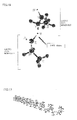
- Fig. 17 Dehydrated condensation of lactic acid molecules results in helical molecules, as described above.
- Molecular model is as shown in Fig. 17 .
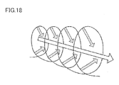
- a sum of vectors of dipoles generated in each molecule is formed, and large dipoles are left in the direction of helix axis.
- the idea is as shown in Fig. 18 .
- PLLA molecules come to have a 10/3 helix structure, in which 10 monomers lead to three turns of helix of molecules. Based on the dipoles in PLLA molecules, if a molecular chain comes to have 10/3 helix structure, the dipole moment in the direction of helix axis is 3.5 to 3.7 debye per one cycle,
- PLLA molecules have molecular weight of several hundreds of thousands, and formed of about 1000 to 3000 cycles. In the following, for simplicity of description, the number of cycles is assumed to be 2000. If this can be oriented as an extended chain, the length will be about 100 nm (in normal lamellar thickness).
- Equation (1) macroscopic piezoelectric stress constant e of polymer is given by Equation (1) below,
- ⁇ Poisson constant
- e' microscopic piezoelectric stress constant.
- e 31 e 31 ⁇ - ⁇ 21 ⁇ e 32 ⁇ - ⁇ 31 ⁇ e 33 ⁇ + 1 - ⁇ 21 ⁇ Ps
- 3 axis is assumed to be in the C axis direction
- Equation (1) The first to third terms of Equation (1) are piezoelectric stress constants derived directly from the molecular structure and very small.
- the fourth term depends on the polarizability Ps and in case of PLLA described here, Ps is very large. Therefore, Equation (1) can be approximated to Equation (2) below.
- Equation (1) can be approximated to Equation (2) below.
- Unstretched film of PLLA has elastic constant of about 3.7 GPa
- 4-times stretched film has elastic constant of about 1.8 GPa.
- C axis is oriented in the direction of stretching.
- the piezoelectric constant of PLLA could possibly be as high as 1000 to 5000 pC/N. Such an implementation, however, has not yet been realized.
- helix axes By arranging helix axes to be vertical to the thickness direction of the film and thereby braking the alternately packed state of dipoles along the C axis by about 10%, or by exploiting about 10% of intrinsic potential of PLLA, it is believed that the value of d 33 as high as 100 to 500 pC/N can be attained (here, 3 axis is in the thickness direction of the film), which is substantially comparable to the piezoelectric constant of PZT.
- the PLLA sheet such as described above can be manufactured in the following manner.
- microwave is applied to a very small region 2 of about 0.01 to about 1 nm 2 of an unprocessed PLLA sheet 1.
- This causes electric field alternation to act on dipoles, resulting in forced vibration of PLEA molecules.
- arrows represent helix axes 3 of PLLA molecules. The direction of each arrow represents the direction of orientation.
- heat generates and makes PLLA molecules more mobile, and by microwave vibration, entangled molecular chains are unraveled.
- helix axes 3 of at least some of PLLA molecules come to be oriented relatively in the thickness direction, to exhibit piezoelectricity in the thickness direction.
- Fig. 1 shows the state of orientation in this region 2.
- PLLA sheet 1 in order to have PLLA sheet 1 exhibit piezoelectricity in the thickness direction at region 2, it is unnecessary to have helix axes 3 of all PLLA molecules oriented in the thickness direction, in a direction not causing cancellation of orientation of dipoles with each other. What is necessary is to have helix axes of only some of the PLLA molecules oriented in the thickness direction. Further, it is not always necessary that helix axes 3 oriented in the thickness direction are vertical (90 degrees) to the main surface direction of PLLA sheet 1. The orientation may be at an angle of 5 to 10 degrees to the main surface direction, and what is essential is that the axes are relatively in the thickness direction.
- region 2 of PLLA sheet 1 is quenched and PLLA molecules are immobilized.
- microwave to be applied not a microwave of single frequency but a plurality of different types of microwaves of different frequencies diplexed or mixed (modulated) is preferred, to include at least microwaves having a frequency mainly suitable for heating, a frequency mainly suitable for shaking main chains and a frequency mainly suitable for breaking molecular bonding to each other. Frequencies and intensities of microwaves may appropriately be determined through experiments.
- region 2 should desirably be a microscopic region. That the region 2 is made larger means the region to be heated is made larger. When the region to be heated is made larger, polymers contained in the region tend to act on each other, leading to growth of crystal referred to as spherocrystal.
- Spherocrystal refers to crystal that grows spherically in radially symmetric manner. Spherocrystal itself is nonpolar and, therefore, the above-described orientation cannot be attained. Therefore, orientation operation of microscopic region not promoting generation of spherocrystal is necessary. Though a smaller region is better, from the viewpoint of practical application, assuming that the region is circular, the area thereof is in the range of 0.01 to 1 mm 2 .
- the size may vary depending on the thickness and molecular weight of PLLA sheet 1 and, if any additive is dispersed in PLLA sheer 1, depending on the type and size of the additive.
- heating with a laser spot may be possible.
- Such an approach has a problem that electrodes for applying strong electric field for realizing orientation of helix axes of PLLA cannot be formed, or the electrodes hinder irradiation of a prescribed position with the laser spot.
- heating of microscopic region with microwaves described in the foregoing is very advantageous in that microwave irradiation and application of DC electric field can be done simultaneously.
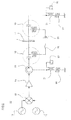
- Fig. 2 is a block diagram showing an apparatus 10 for manufacturing the piezoelectric sheet in accordance with an embodiment of the present invention.
- manufacturing apparatus 10 prescribed process steps are executed on a prepared PLLA sheet 1 to manufacture the piezoelectric sheet.
- Microwaves for vibrating molecules of PLLA constituting PLLA sheet 1 are generated by signal generators 11 and 12. Though two signal generators 11 and 12 are used in the example of Fig. 2 , the number of generators may appropriately be changed in accordance with the number of different types of microwaves to be applied.
- the generated microwaves are adapted to have a frequency mainly for heating PLLA, a frequency mainly for unraveling entangled molecules, and a frequency mainly for breaking molecular bonding with each other (partial crystallization). These frequencies vary depending on the molecular weight of PLLA as the material blend ratio of D-form, crystallinity, degree of orientation and the amount of filler. Therefore, optimal frequency and level of application may be determined by conducting initial experiments for each base material to be used.
- the ratio of input levels of microwaves having different frequencies is determined by output levels of signal generators 11 and 12.
- a plurality of different types of microwaves having frequencies different from each other emitted from signal generators 11 and 12 are mixed by a mixer 13 and, thereafter, transmitted to an amplifier 14,
- mixer 13 is used in the example shown in Fig. 2 to mix a plurality of different types of microwaves having frequencies different from each other, a diplexer may be used in place of mixer 13. Further, the number of signal generators may be increased and a triplexer or quadplexer may be used.
- the microwaves amplified by amplifier 14 pass through a circulator 15 and a bias tee 16, and reach a PLLA heating unit 17.
- Circulator 15 is provided to prevent reflected power resulting from mismatch of PLLA heating unit 17 from returning to amplifier 14 to damage amplifier 14.
- the reflected power resulting from mismatch of PLLA heating unit 17 is branched by circulator 15, passes through a coupler 21 and reaches attenuator 22, where the power is consumed.
- a power meter 23 is connected to coupler 21 to monitor the reflected power.
- PLLA heating unit 17 is configured to prevent passage of DC current therethrough, PLLA heating unit 17 may have a transmission line type configuration or a resonator included configuration. In Fig. 2 , PLLA heating unit 17 is simply depicted as a capacitor and, actually, a microwave equivalent circuit is formed. In any case, PLLA heating unit 17 has a portion where a capacitor is formed with PLLA sheet 1 when viewed as a circuit, in a path through which electric power passes, whereby passage of DC current is prevented. Details of PLLA heating unit 17 are shown in Fig. 3 and following figures. Description with reference to Fig. 3 and following figures will be given later.
- PLLA heating unit 17 has a portion where a capacitor is formed with PLLA sheet 1 when viewed as a circuit, in a path through which electric power passes, When microwave passes through this portion, part of the wave is converted to heat because of dielectric loss.
- Dielectric tangent (tan ⁇ ) of PLLA is 0.01 to 0.012 (for example, see Japanese Patent Laying-Open No. 2002-358829 ) and in a capacitor using PLLA as a dielectric, heat inevitably generates in accordance with tan ⁇ . In addition, heat also generates by friction of electric dipoles.
- a power meter 26 is connected to coupler 24 to monitor electric power passed therethrough.
- the electric power consumed by PLLA heating unit 17 can indirectly be grasped.
- the electric power consumed by PLLA heating unit 17 represents energy converted to heat on PLLA sheet 1 and from this value, it is possible to roughly know to what temperature PLLA sheet 1 is heated. To be exact, the temperature of PLLA sheet 1 may be directly measured using, for example, an infrared contact-free thermometer.
- Melting point of PLLA is approximately at 170°C, and it has been confirmed through experiments that temperature of approximately 140°C to 150°C is suitable for controlling orientation of molecules.
- the temperature varies depending on the molecular weight of PLLA, additives, and processing of terminal group of molecules and, therefore, it is selected appropriately for actually used PLLA sheet 1,
- a high voltage DC power supply 20 and a switch 19 are connected to bias tees 16 and 18.
- switch 19 is turned on, to apply high voltage to PLLA sheet 1.
- At least some of the dipoles shaken by the microwaves are oriented, by the electric field generated by the high voltage, relatively in the thickness direction (the direction of the electric field).
- the magnitude and time of application of the voltage also depend on the molecular weight, additives, and processing of terminal group of molecules and, therefore, it is selected appropriately for actually used PLLA sheet 1.
- the microwaves and the high voltage are applied for a prescribed time period and, simultaneously with stopping the application, PLLA sheet 1 is subjected to forced quenching, so that the molecules are immobilized. It is not always necessary, however, that the timing of cooling be immediately after the stop of application of microwaves and high voltage.
- Application of microwaves and high voltage may be stopped after the start of cooling, or application of microwaves may be stopped first, followed by the start of cooling and then application of high voltage may be stopped.
- Fig. 3 shows details of a PLLA processing unit 30 including PLLA heating unit 17, with PLLA heating unit 17 on the block diagram of Fig. 2 configured as a transmission line type unit.
- (a) of Fig. 3 is a plan view of PLLA processing unit 3
- (b) of Fig. 3 is a front view of PLLA processing unit 3.
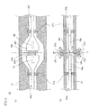
- (a) of Fig. 4 is a cross-sectional view taken along line A-A of Fig. 3(b)
- (b) of Fig. 4 is a cross-sectional view taken along line B-B of Fig. 3(a) .
- PLLA processing unit 30 has a housing 31, and holes 33 and 34 for inserting PLLA sheet 1 are formed in housing 31. As is well shown in Fig. 4(b) , holes 33 and 34 are formed to pass through upper and lower walls of housing 31. PLLA sheet 1 is inserted through holes 33 and 34 and processed in this state.
- a pair of guide rollers 32a and 32b and a pair of guide rollers 32c and 32d are provided, and PLLA sheet 1 is held by these guide rollers 32a to 32d.
- PLLA sheet 1 can be moved in up/down directions of Figs. 3(b) and 4(b) .
- Arrows around guide rollers 32a to 32d and an arrow above PL-LA sheet 1 shown in Tig. 4(b) represent an example of the direction of rotation of guide rollers 32a to 32d and direction of movement of PLLA sheet 1.
- Driving unit for driving guide rollers 32a to 32d is not shown.
- Housing 31 is formed of metal and configured as an outer conductor of coaxial line, while forming a cavity inside.
- Preferable metal used for forming housing 31 may include copper, aluminum, brass, iron and stainless steel and, such metal may be plated as needed. When iron or stainless steel is used, since it has low electric conductivity, copper plating or silver plating is preferred in consideration of transmission loss.
- inner conductors 35a and 35b as inner conductors (central conductors) of coaxial line are arranged, held by insulators 37a and 37b.
- insulators 37a and 37b are formed of resin having low dielectric constant and, particularly, polytetrafluoroethylene is a preferred material.
- Inner conductors 35a and 35b have tip ends 38a and 38b opposed to each other, respectively, and tip ends 38a and 38b are made wider than other portions as can be well seen from Fig. 4(a) .
- tip ends 38a and 38b having the widened shape a plurality of pin conductors 36a and 36b as conductors for applying high voltage are provided to form pairs with each other without leaving any unpaired conductor.
- the coaxial line implemented by housing 31 and inner conductors 35a and 35b is formed to have characteristic impedance of 50 ⁇ except for the portion where the cavity is made larger at the central portion in the axial direction, to facilitate matching with a high frequency device. Further, the cavity in housing 31 is enlarged in tapered manner at the central portion along the axial direction, and inner conductors 35a and 35b also have tip ends 38a and 38b widened in a tapered manner corresponding to the taper of the cavity, Because of this structure, smooth impedance conversion is possible, and power reflection caused by impedance mismatch is minimized.
- PLLA processing unit 30 is formed as a transmission line type unit and, therefore, it can be applied to a very wide range of frequencies, and design and manufacturing are relatively easy,
- Each of pin conductors 36a and each of pin conductors 36b are positioned to be opposite to and aligned on the same axial line with each other.
- PLLA sheet 1 is pinched by pin conductors 36a and 36b opposite to each other. Between each pair of opposite pin conductors 36a and 36b, a small capacitor is formed.
- the diameter of each of pin conductors 36a and 36b is about 0.1 mm to about 1 mm, and the space between adjacent ones of pin conductors 36a and 36b is set to be at least the radius of each of pin conductors 36a and 36b.
- the number of pin conductors 36a and 36b may be appropriately selected .
- the diameter of each of pin conductors 36a and 36b should preferably be small, since it must be small enough to prevent formation of spherocrystal in PLLA sheet 1.
- pin conductors 36a and 36b pinching PLLA sheet 1 form pairs on opposite sides of PLLA sheer 1 the conductors may be formed as pin conductors on one side and as a planar conductor on the other side. Such a configuration will be described as an example with reference to a PLLA processing unit 50.
- Pin conductors 36a and 36b forming pairs as shown in Fig. 4 are suitable for heating smaller regions of PLLA sheer 1, while a configuration having pin conductors on one side and a planar conductor on the other side is advantageous in that assembly of the apparatus is very simple.
- Inner conductors 35a and 35b and pin conductors 36a and 36b are formed of metal, as is housing 31 .
- Suitable metal used here may include copper, aluminum, brass, iron, stainless steel, invar and 42 alloy and, such metal may be plated as needed.
- iron, stainless steel, invar or 42 alloy since it has low electric conductivity, copper plating or silver plating is preferred in consideration of transmission loss,
- inner conductors 35a and 35b and pin conductors 36a and 36b should preferably be formed using a material having relatively low thermal conductivity such as iron, stainless steel, invar or 42 alloy.
- pin conductors 36a and 36b should preferably be formed of invar or 42 alloy, additionally considering thermal expansion.
- pin conductors 36a and 36b Preferable arrangement of pin conductors 36a and 36b will be described later with reference to Figs. 10 to 13 .
- microwaves are input to locally heat PLLA sheet 1, to have helix axes of at least some of the PLLA molecules oriented relatively in the thickness direction, and thereafter, the sheet is quenched to have PLLA molecules immobilized.
- a cooling gas is introduced to the inner cavity of housing 31.
- a passage for introducing cooling gas is not shown in Figs. 3 and 4 , it is preferred to provide a passage through which cooling gas flows inside inner conductors 35a and 35b and, at the time of quenching, to have the cooling gas emitted from outlets provided near pin conductors 36a and 36b directly to PLLA sheet 1, Specific example of the configuration for cooling will be described with reference to Fig. 5 later.
- Inner conductors 35a and 35b are movable in directions indicated by arrows 39 and 40 in Fig. 4(a) , respectively. After the end of processing, inner conductors 35a and 35b are moved to release pinching of PLLA sheet 1, and then, guide rollers 32a to 32d are rotated to move PLLA sheet 1 by a prescribed distance. After moving PLLA sheet 1, inner conductors 35a and 35b are again moved, to pinch PLLA sheet 1 between pin conductors 36a and 36b, and the above-described process steps of microwave heating, high voltage application and quenching are executed. By repeating such operations, a PLLA sheet 1 having high piezoelectric constant, in which helix axes are oriented relatively in the thickness direction over a wide range, can be obtained.
- FIG. 5 shows, in a cross-section, one inner conductor 35a shown in Fig. 4 , and one end of transmission line portion including housing 31 and inner conductors 35a and 35b, which are not shown in Fig. 4 .
- inner conductor 35a is formed to have an inner cavity, and on an end surface of tip end 38a where pin conductors 36a are provided, a plurality of outlets 41 are formed near each position of pin conductor 36a.
- Current caused by microwaves flow through a surface layer of inner conductor 35a because of skin effect and, therefore, the inner cavity of inner conductor 35a does not have any influence on the transmission current of microwaves.
- Inner conductor 35a is connected to another inner conductor 42 to transmit without reflection the electric power transmitted from inner conductor 42.
- a coaxial line, on which inner conductor 42 is positioned, is also adapted to have characteristic impedance of 50 ⁇ .
- a tube 43 formed, for example, of polytetrafluoroethylene is inserted. Cooling gas is introduced to tube 43 from the direction of an arrow 44, and blown out in the direction of an arrow 45 through outlet 41, so as to cool pin conductors 36a and PLLA sheet 1 (not shown in Fig. 5 ).
- HCFC (-134a) or LPG may be suitably used as the cooling gas.
- a liquid may be used.
- Liquid nitrogen may suitably be used as the liquid. In that case, preferably, liquid nitrogen is sprayed from outlets 41.
- the configuration for cooling such as described above may be provided only on the side of inner conductor 35a or only on the other inner conductor 35b, or may be provided both on inner conductors 35a and 35b.
- PLLA sheet 1 can be cooled with high efficiency, and cooling gas or liquid can be used without waste.
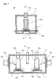
- Fig. 6 shows details of PLLA processing unit 50 including PLLA heating unit 17, with PLLA heating unit on the block diagram of Fig. 2 configured as a resonator included unit.
- (a) of Fig. 6 is a front view of PLLA processing unit 50 and (b) of Fig. 6 is a cross-sectional view of PLLA processing unit 50.
- Fig. 7 includes (a) a cross-sectional view taken along line B-B of Fig. 6(b) and (b) a cross-sectional view taken along line A-A of Fig. 6(a) .
- PLLA processing unit 50 has a housing 51, and holes 55a and 55b for inserting PLLA sheet 1 are formed in housing 51.
- a hole similar to hole 55a is formed in a wall opposite to the wall having hole 55a formed therein.
- a hole similar to hole 55b is formed in a wall opposite to the wall having hole 55b formed therein.
- PLLA sheets 1 are arranged to be inserted through hole 55a and the opposite hole and through hole 55b and the opposite hole.
- guide rollers corresponding to guide rollers 32a to 32d provided in PLLA processing unit 30 shown in Figs. 3 and 4 described above are not shown.
- Housing 51 is formed of a metal having high electric conductivity.
- Preferable metal used may include copper, aluminum, brass, iron and stainless steel and, such metal may be plated as needed.
- copper plating or silver plating is preferred in consideration of transmission loss.
- Housing 51 has a function of shielding electromagnetic waves, and its inner cavity serves as a resonant cavity.
- PLLA processing unit 50 constitutes a semiaxial cavity filter
- Housing 51 functions as an outer conductor of the semiaxial cavity filter.
- the example shown in Figs. 6 and 7 forms a two-stage band-pass filter.
- connectors 52a and 52b are provided as input/output units for supplying electric power to the filter. Since such a band-pass filter basically has a symmetrical shape, either of connecters 52a and 52b may be used as an input or output. For convenience, here, description will be given assuming that connector 52a is the input side and connector 52b is the output side.
- a central conductor of connector 52a To a central conductor of connector 52a, one end of an input lead 56a formed of a metal line is connected. The other end of input lead 56a is connected to a central conductor 57a. On one end of central conductor 57a, a plurality of pin conductors 58a are provided. A base electrode 60a providing a planar conductor is arranged to oppose to the tip ends of pin conductors 58a. Between tip ends of pin conductors 58a and base electrode 60a, there is a small space, in which PLLA sheet 1 is held. At this portion, an equivalent circuit of a capacitor is formed. The other end of central conductor 57a is spaced by a prescribed distance from and opposes to tip end of a frequency adjustment screw 53a.
- an output lead 56b, a central conductor 57b, pin conductors 58b, a base electrode 60b and frequency adjustment screw 53b provided in relation to connector 52b are configured and arranged in the similar manner as output lead 56a, central conductor 57a, pin conductors 58a, base electrode 60a and frequency adjustment screw 53a provided in relation to connecter 52a described above.
- a joint adjustment screw 54 is inserted near the mid-point of central conductors 57a and 57b.
- PLLA sheet 1 is pinched between pin conductors 58a and base electrode 60a, or between pin conductors 58b and base electrode 60b.
- pin conductors may be arranged in place of base electrodes 60a and 60b, to be paired with each of pin conductors 58a and 58b.
- the filter can be adjusted to desired characteristics, within the range of original electric design.
- Central conductors 57a and 57b, frequency adjustment screws 53a and 53b, joint adjustment screws 54, base electrodes 56a and 56b, and pin conductors 58a and 58b are formed of metal.
- metal used here may include copper, aluminum, brass, iron and stainless steel and, such metal may be plated as needed.
- copper plating or silver plating is preferred in consideration of transmission loss,
- central conductors 57a and 57b are fixed on housing 51 by insulating material having low dielectric constant.
- Polytetrafluoroethylene is a preferred material of low dielectric conductivity.
- pin conductors 58a and 58b are similar to that in PLLA processing unit 30 and, therefore, description thereof will not be repeated.
- base electrodes 60a and 60b On base electrodes 60a and 60b, a recessed portion (spot face) 61 opened outward is formed as shown in Fig. 7(a) , and a bottom wall 62 of recessed portion 61 is formed very thin. Specifically, thickness of bottom wall 62 is preferably about 0.3 to abort 0.8 mm.
- Base electrodes 60a and 60b are preferably formed of metal having high thermal conductivity and, by way of example, aluminum or copper is preferably used.
- PLLA sheet 1 pinched between pin conductors 58a and 58b and base electrodes 60a and 60b is heated by the input of microwaves, As described above, to the heated PLLA sheet 1, high voltage is applied and, thereafter, the sheet must be quenched.
- bottom wall 62 By directly blowing cooling gas to bottom wall 62 of recessed portion 61, bottom wall 62 can be cooled instantaneously.
- bottom wall 62 is formed of metal having high thermal conductivity and is sufficiently thin, PLEA sheet 1 is also cooled substantially simultaneously.
- the cooling gas is the same as that described above.
- PLLA processing unit 50 has a resonator induced configuration, electric field strength applied to PLLA sheet 1 is significantly higher than in the transmission line type unit and, in a filter designed to have central frequency of 2.4GHz, the electric field strength is 100 times higher than in the transmission line type unit.
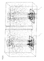
- Fig. 8 shows a result of finite element method simulation, using a simplified model of PLLA processing unit 50.
- arrows represent electric field vectors, whose size indicates electric field intensity. It can be seen that very large electric field vector exists at the position where PLLA sheet 1 is inserted. Therefore, by PLLA processing unit 50, at the time of heating with microwaves, amplifier output can be made lower than in the transmission line type unit.
- PLLA processing unit 50 shown in Figs. 6 and 7 form a two-stage band-pass filter. It may be used as a single-stage band-pass filter using only one semiaxial resonator. In that case, the band-pass filter passes only the frequencies near the pole including the resonant frequency and, therefore, it is for very narrow band and the frequency to be input is limited, On the other hand, it is possible to increase the number of stages of the filter. It may be implemented as a filter of two-stage to about 10 stages as needed. Though the number of stages is not limited, experimentally, up to 10 stages is preferred, considering the time and effort necessary for fabrication. A filter having fractional bandwidth of about 4% may be fabricated relatively easily, with about 4 to about 8 stages. Assuming that the central frequency of passband at this time is 2GHz, the filter will be a band-pass filter having bandwidth of 70 MHz and, hence, an apparatus capable of simultaneously applying a plurality of frequencies can be obtained.
- Fig. 9 shows an example in which the PLLA processing unit is formed as a four-stage band-pass.
- Fig. 9 corresponds to Fig. 7(b) .
- components corresponding to those shown in Fig. 7(b) are denoted by the same reference characters and description thereof will not be repeated.
- PLLA processing unit 50a shown in Fig. 9 incudes central conductors 57c and 57d in addition to central conductors 57a and 57b, and includes frequency adjustment screws 53c and 53d in addition to frequency adjustment screws 53a and 53b. Further, the unit includes three joint adjustment screws 54a, 54b and 54c.
- the microwave heating unit for PLLA sheet 1 can surely be provided on the input stage or output stage or on both input and output stages, In a multi-stage band-pass filter, relatively large energy is accumulated at the input/output stage and, therefore, electric field strength is high at these portions. Further, since high voltage is applied through bias tees 16 sand 18 (see Fig. 2 ), the high voltage can easily be applied at the input/output stage directly connected by the conductors from the central conductor of transmission line (connector).
- FIG. 10 to 13 show pin conductors 36a with an end surface at a tip end 38a of inner conductor 35a viewed from the side of PLLA sheet 1.
- outlets 41 shown in Fig. 5 described above are not shown.
- pin conductors 36b on the other side are not shown and description will not be given, these are arranged substantially in symmetry with pin conductors 36a shown in the figures,
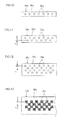
- a plurality of pin conductors 36a are arranged in a line, spaced apart from each other by a prescribed distance.
- the PLLA sheet is shifted in the up/down direction or left/right direction by a prescribed distance and, in this state, the series of process steps for imparting piezoelectricity is executed again, and such operations are repeated.
- the process for imparting piezoelectricity is done.
- a plurality of pin conductors 36a are arranged in two lines, spaced apart from each other by a prescribed distance. Pin conductors 36a of each line are positioned to correspond to the space between each of the pin conductors 36a of the other line,
- the PLLA sheet is shifted upward (or downward) by distance d and, in this state, the series of process steps for imparting piezoelectricity is executed again, and such operations are repeated.
- the process for imparting piezoelectricity is done over a wide range of PLLA sheet.
- a plurality of pin conductors 36a are arranged in four lines, spaced apart from each other by a prescribed distance. Pin conductors 36a of each line are positioned to correspond to the space between each of the pin conductors 36a of the next line.
- the PLLA sheet is shifted upward (or downward) by distance d and, in this state, the series of process steps for imparting piezoelectricity is executed again. Thereafter, the PLLA sheet is shifted upward (or downward) by three times the distance d and, in this state, the series of process steps for imparting piezoelectricity is executed again. Then, again, the PLLA sheet is shifted upward (or downward) by the distance d and, in this state, the series of process steps for imparting piezoelectricity is executed. Thereafter, shifting by three times the distance d and shifting by the distance d are executed alternately while the operations as described above are repeated. Thus, the process for imparting piezoelectricity is done over a wide range of PLLA sheet.
- Fig. 12 is the most advantageous, and the example shown in Fig. 11 is the second most advantageous in that the process for imparting piezoelectricity can be executed collectively over a wider area.
- the dimension of inner conductors 35a and 35b and the number of pin conductors 36a and 36b to be arranged in the widthwise and lengthwise directions may be appropriately selected in accordance with design.
- the cross section of pin conductors 36a and 36b may not necessarily be circular.
- the cross section may be oval, elliptical, square or polygonal.
- Fig. 13 shows an example in which pin conductors 36a each have a square cross-section.
- the arrangement of pin conductors 36a shown in Fig. 13 is substantially the same as that shown in Fig. 12 . It is noted, however, that the distance between adjacent pin conductors 36a is made equal to the length of one side of the square defining the cross section of each pin conductor 36.
- pin conductors 36a are hatched.
- pin conductors 36a and 36b described with reference to Figs, 10 to 13 may be adopted for the arrangement of pin conductors 58a and 58b shown in Figs. 7 and 9 .
Landscapes
- Engineering & Computer Science (AREA)
- Manufacturing & Machinery (AREA)
- Chemical & Material Sciences (AREA)
- Physics & Mathematics (AREA)
- Spectroscopy & Molecular Physics (AREA)
- Polymers & Plastics (AREA)
- Organic Chemistry (AREA)
- Health & Medical Sciences (AREA)
- Medicinal Chemistry (AREA)
- Chemical Kinetics & Catalysis (AREA)
- Biological Depolymerization Polymers (AREA)
- Manufacture Of Macromolecular Shaped Articles (AREA)
- Treatments Of Macromolecular Shaped Articles (AREA)
Abstract
Description
- The present invention relates to a piezoelectric sheet and to method and apparatus for manufacturing the piezoelectric sheet and, more specifically, it relates to a piezoelectric sheet composed of polylactic acid as well as method and apparatus for manufacturing the same.
- Polylactic acid (PLA) has such a molecular structure as shown in
Fig. 14 . PLA is dehydrated condensation polymer obtained through ring-opening polymerization of lactide, which is a cyclic dimer of lactic acid. Since lactic acid contains asymmetric carbon, it has chirality, Therefore, L-form and D-from are present in PLA, whose polymers are referred to as poly L-lactic acid (PLLA) and poly D-lactic acid (PDLA), respectively. Main chain of PLLA has left-handed helix structure, and main chain of PDLA has right-handed helix structure. Polylactic acid derived from lactic acid synthesized by microorganism is mostly in L-form and, currently mass-produced and used PLA is PLLA. - As described, for example, in
Patent Literature 1 andNon-Patent Literature 1, a stretched PLA film exhibits piezoelectricity. According toNon-Patent Literature 1, point group of PLLA crystal is D2, and has such component as shown inFig. 15(a) as piezoelectric tensor. - PLLA is helical polymer having dipoles of large value in the helix axis direction (C-axis direction). Crystal structure of PLLA is packed with dipoles in the C-axis direction facing opposite directions alternately. Therefore, macroscopically, dipoles in the C-axis direction are cancelled with each other to be zero. Therefore, assuming that a PLLA sheet is stretched in "3" axis direction as shown in
Fig. 15(b) , the piezoelectric tensor of the stretched, uniaxially-oriented PLLA sheet comes to have such component as shown inFig. 15(c) as a result. - As described, for example, in
Patent Literatures Fig. 15(c) , of which value is about 10 to 20pC/N. The piezoelectric constant of PLLA is distinctively high among polymers. - On the other hand, PZT as a representative example of ceramic piezoelectric body commercially available at present has as high a value as d33 = 300 to 700 pC/N, and it is applied to various actuators, piezoelectric and piezoelectric speakers. PZT, however, is lead-containing material and, from the viewpoint of environmental projection, lead-free piezoelectric material has been desired in the market. Further, among inorganic piezoelectric materials, ceramics are dominant, of which manufacturing cost is high and which inevitably involves disposal by landfill, From the foregoing, polymer piezoelectric material that can be manufactured at a low cost and is easily disposable has been desired. No material having piezoelectric constant comparable to PZT has said to be found.
- PVDF (polyvinylidenefluoride) and PLLA are considered promising as polymers having very high piezoelectric constants. Particularly, as can be seen from
Fig. 14 , PLLA contains only C, O and H as constituent elements and, therefore, it will not emit any harmful substance when incinerated, Further, PLLA is biodegradable plastic that can be fully decomposed to water and CO2 through two of decomposition process of hydrolysis and microbial degradation. At present, raw material is corn starch, and petroleum oil is not at all used as the raw material. Except for CO2 derived from energy used in the manufacturing process, PLLA itself does not increase CO2 in the air after decomposition, since original material of PLLA is CO2 in the air. This is the reason why PLLA is considered carbon-neutral, and it attracts attention as environmentally friendly material. - It is noted, however, that piezoelectric constant of PLLA is, for d14, at most 20 pC/N, which is very low as compared with the piezoelectric constant of PZT. In order to use PLLA as a replacement of PZT, it is necessary to apply very high voltage at the time of operation. Therefore, conventionally, replacement to PLLA has been very difficult.
-
- PTL 1: Japanese Patent Laying-Open No.
5-152638 - PTL 2: Japanese Patent Laying-Open No.
2005-213376 -
- NPL 1: Yoshiro TAJITSU, "Poly Nyusan Maku no Hikari/Denki Kinou (Optical/Electric Functions of Polylactic Film)", Mirai Zairyo, July 2003, Vol. 3, No. 7, pp. 16-25.
- In view of the foregoing, an object of the present invention is to provide a piezoelectric sheet having high piezoelectric constant particularly in thickness direction, using polylactic acid.
- Another object of the present invention is to provide method and apparatus for manufacturing a piezoelectric sheet such as described above.
- The first aspect of the present invention is directed to a piezoelectric sheet composed of polylactic acid having helix of at least some polylactic acid molecules oriented relatively in thickness direction, to exhibit piezoelectricity in the thickness direction, in order to solve the technical problem described above.
- It is noted that the term "sheet" and the term "film" are sometimes used separately to represent different thicknesses. In the present specification, however, the term "sheet" will be used regardless of the thickness.
- Further, as described in the Background section, commonly distributed polylactic acid is poly L-lactic acid. It is noted, however, that the polylactic acid described as a solution to the technical problem encompasses, in concept, poly L-lactic acid, poly D-lactic acid and the mixture of these.
- The invention is also directed to a method of manufacturing the piezoelectric sheet described above. The method of manufacturing a piezoelectric sheet in accordance with the present invention includes the steps of: preparing a polylactic acid sheet; heating the polylactic acid sheet using a microwave; and applying a high voltage in thickness direction of the heated polylactic acid sheet, to orient helix axes of at least some of polylactic molecules relatively to the thickness direction, to have piezoelectricity exhibited in the thickness direction of the polylactic acid sheet.
- Preferably, the method of manufacturing a piezoelectric sheet according to the present invention further includes the of quenching the polylactic acid sheet after the step of applying high voltage.
- Preferably, in the method of manufacturing a piezoelectric sheet according to the present invention, the step of applying high voltage is executed simultaneously with at least part of the heating step.
- The present invention is also directed to an apparatus for manufacturing the piezoelectric sheet described above. The apparatus for manufacturing the piezoelectric sheet in accordance with the present invention incudes a high voltage power supply; conductors for applying high voltage, forming a pair arranged to hold therebetween a polylactic acid sheet in thickness direction, for applying a high voltage supplied from the high voltage power supply in the thickness direction of the polylactic acid sheet to be processed; a microwave generator for generating a microwave; and a coaxial line transmitting the microwave from the microwave generator; wherein the conductors for applying high voltage are connected to an inner conductor of the coaxial line, and adapted to generate heat by dielectric loss, when the microwave passes through a capacitor formed by the polylactic acid sheet and the conductors for applying high voltage holding the sheet.
- According to another embodiment, the apparatus for manufacturing a piezoelectric sheet in accordance with the present invention includes a high voltage power supply; conductors for applying high voltage, forming a pair arranged to hold therebetween a polylactic acid sheet in thickness direction, for applying a high voltage supplied from the high voltage power supply in the thickness direction of the polylactic acid sheet to be processed; a microwave generator for generating a microwave; a coaxial line transmitting the microwave from the microwave generator; and at least one stage of semiaxial cavity filter connected to the coaxial line; wherein one of the conductors for applying high voltage is connected to a central conductor of the semiaxial cavity filter, the other one of the conductors for applying high voltage is connected to an outer conductor of the semiaxial cavity filter, and the conductors for applying high voltage are adapted to generate heat by dielectric loss, when the microwave passes through a capacitor formed by the polylactic acid sheet and the conductors for applying high voltage.
- In the apparatus for manufacturing a piezoelectric sheet in accordance with the present invention, one of the conductors for applying high voltage may be implemented by a plurality of pin-shaped conductors, and the other of the conductors for applying high voltage may be implemented by a planar conductor. Alternatively, one and the other of the conductors for applying high voltage may be implemented by a plurality of pin-shaped conductors, and the plurality of pin-shaped conductors may form pairs with each other without leaving any unpaired conductor.
- In the apparatus for manufacturing a piezoelectric sheet in accordance with the present invention, preferably, a plurality of different types of microwaves having frequencies different from each other are generated by the microwave generator, Preferably, the plurality of different types of microwaves include at least a microwave having a frequency mainly effective for heating, a microwave having a frequency mainly suitable for shaking main chain of polylactic acid, and a microwave having a frequency mainly suitable for braking bonding portion bonding polylactic acid molecules with each other.
- In the apparatus for manufacturing a piezoelectric sheet in accordance with the present invention, preferably, if the conductor for applying high voltage is implemented by a plurality of pin-shaped conductors, the plurality of pin-shaped conductors are arranged to form a plurality of lines, and each of the pin-shaped conductors of each line is positioned corresponding to a space formed between each of the conductors of an adjacent line. More preferably, the conductor has a square cross section, and the space between adjacent conductors is made equal to length of one side of the square defining the cross section of each conductor.
- In the apparatus for manufacturing the piezoelectric sheet in accordance with the present invention, preferably, an outlet of cooling fluid is provided close to the conductor for applying high voltage, for quenching the polylactic acid sheet.
- A polylactic acid sheet in a bulk state (formed but unprocessed) has a structure having long helical molecules entangled with each other and, even if a very large electric field is applied in the thickness direction, piezoelectricity is not exhibited in the thickness direction. According to the present invention, in a piezoelectric sheet composed of polylactic acid, the entangled helical molecules are unraveled, and at least in some helical molecules, helix axes are relatively oriented in the thickness direction. Thus, a piezoelectric sheet exhibiting piezoelectricity in the thickness direction can be obtained. If only 10% of helical molecules could be oriented in the thickness direction of the piezoelectric sheet, a piezoelectric body comparable to ZIT would be obtained. If higher ratio of molecules could be oriented, a piezoelectric body superior to PZT would result. Even if the ratio is as low as 5%, the resuming piezoelectric body would have remarkably high piezoelectric constant for a polymer piezoelectric body.
- PZT widely used for piezoelectric actuators and the like is lead-containing ceramic, which is difficult to dispose of. If piezoelectric constant comparable to PZT can be attained in PLLA, replacement of PZT with PLLA becomes possible. PLLA is biological polymer of simple composition not including heavy metal, which is biodegradable and formed from starch as raw material. Therefore, it does not increase CO2 in the air except for CO2 generated at the time of manufacturing. Further, CO2 generated at the time of manufacturing is quite small in amount as compared with manufacturing of other organic polymers. Therefore, replacement of PZT with PLLA has great effect in reducing environmental load,
- Further, since polylactic acid is polymer and has higher flexibility than PZT, it attains higher amount of displacement than PZT when applied to an actuator.
-
-
Fig. 1 is a cross-sectional view of a PLLA sheer 1, illustrating a state in which at least some ofhelix axes 3 of PLLA molecules are relatively oriented in the thickness direction, by the manufacturing method of the present invention. -
Fig. 2 is a block diagram showing amanufacturing apparatus 10 in accordance with an embodiment of the present invention. -
Fig. 3 includes (a) a plan view of aPLLA processing unit 30 and (b) a front view ofPLLA processing unit 30, showing details ofPLLA processing unit 30 including aPLLA heating unit 17, withPLLA heating unit 17 on the block diagram ofFig. 2 configured as a transmission line type unit. -
Fig. 4 includes (a) a cross-sectional view taken along line A-A ofFig. 3(b) and (b) a cross-sectional view taken along line B-B ofFig. 3(a) . -
Fig. 5 correspond to (a) and (b) ofFig. 4 , showing, in a cross-section, oneinner conductor 35a shown inFig. 4 , and one of transmission line portion including ahousing 31 andinner conductors Fig. 4 . -
Fig. 6 incudes (a) a front view of aPLLA processing unit 50 and (b) a cross-sectional view ofPLLA processing unit 50, showing details ofPLLA processing unit 50 includingPLLA heating unit 17, with PLLA heating unit on the block diagram ofFig, 2 configured as a resonator included unit. -
Fig. 7 includes (a) a cross-sectional view taken along line B-B ofFig. 6(b) and (b) a cross-sectional view taken along line A-A ofFig. 6(a) . -
Fig. 8 shows a of electric field obtained through finite element method simulation, using a simplified model ofPLLA processing unit 50 shown inFigs. 6 and7 . -
Fig. 9 corresponds toFig. 7(b) , showingPLLA processing unit 50a formed as a four-stage band-pass. -
Fig. 10 shows a first example of an arrangement ofpin conductors 36a shown inFig. 4 , showingpin conductors 36a with an end surface at atip end 38a ofinner conductor 35a viewed from the side ofPLLA sheet 1. -
Fig. 11 shows a second example of an arrangement ofpin conductors 36a shown inFig. 4 , showingpin conductors 36a with an end surface at atip end 38a ofinner conductor 35a viewed from the side ofPLLA sheet 1. -
Fig. 12 shows a third example of an arrangement ofpin conductors 36a shown inFig. 4 , showingpin conductors 36a with an end surface at atip end 38a ofinner conductor 35a viewed from the side ofPLLA sheet 1. -
Fig. 13 shows a fourth example of an arrangement ofpin conductors 36a shown inFig. 4 , showingpin conductors 36a with an end surface at atip end 38a ofinner conductor 35a viewed from the side ofPLLA sheet 1. -
Fig. 14 shows molecular structure of polylactic acid. -
Fig. 15 shows (a) piezoelectric tensor of PLLA crystal, (b) direction of stretching PLLA sheet, and (c) piezoelectric tensor of uniaxially-oriented PLLA sheet. -
Fig. 16 illustrates two bonded lactic acid molecules. -
Fig. 17 illustrates lactic acid molecules forming helical molecules through dehydrated condensation. -
Fig. 18 illustrates a function of helix axis of the lactic acid molecules shown inFig. 17 . - PLLA has such a molecular structure as shown in
Fig. 14 , as described above, and on a main chain, there is a molecular group generating permanent dipoles, such as C= O. When we consider two bonded lactic acid molecules, electric dipoles such as shown inFig. 16 appear. - As described above, polylactic acid includes PLLA as L-form and PDLA as D-form, and a positive mixture of these may be considered. In this section, however, description will be given with reference to PLLA as an example, for simplicity of description.
- Dehydrated condensation of lactic acid molecules results in helical molecules, as described above. Molecular model is as shown in
Fig. 17 . In the molecules of helical structure of PLLA, a sum of vectors of dipoles generated in each molecule is formed, and large dipoles are left in the direction of helix axis. The idea is as shown inFig. 18 . - As shown in
Fig. 18 , PLLA molecules come to have a 10/3 helix structure, in which 10 monomers lead to three turns of helix of molecules. Based on the dipoles in PLLA molecules, if a molecular chain comes to have 10/3 helix structure, the dipole moment in the direction of helix axis is 3.5 to 3.7 debye per one cycle, - Generally, PLLA molecules have molecular weight of several hundreds of thousands, and formed of about 1000 to 3000 cycles. In the following, for simplicity of description, the number of cycles is assumed to be 2000. If this can be oriented as an extended chain, the length will be about 100 nm (in normal lamellar thickness).
- Here, the sum of dipoles of the molecules will be

- In the following, for simplicity of description, it is assumed to be 7200 debye.
- Here, 1 debye = 3.33564 × 10⁻³⁰ C·m and, therefore, 7200 debye = 2.4 × 10⁻²⁶ C·m.
- Assuming that two molecular chains are aligned parallel to each other, adjacent molecular chains come close to each other near the radius of PLLA helix, and from the correlation distance of higher order structure of amorphous and crystal structures of PLLA, the distance between helix axes is estimated to be 0.4 to 0.8 nm. In the following, for simplicity of description, the value is assumed to be 0.4 nm.
- Here, polarizability Ps is given as

- Using polarizabilitly Ps, macroscopic piezoelectric stress constant e of polymer is given by Equation (1) below, In Equation (1), ν represents Poisson constant and e' represents microscopic piezoelectric stress constant.

- The first to third terms of Equation (1) are piezoelectric stress constants derived directly from the molecular structure and very small. The fourth term depends on the polarizability Ps and in case of PLLA described here, Ps is very large. Therefore, Equation (1) can be approximated to Equation (2) below.


- Since Ps = 3.0 C/m2 as mentioned above,

- Here, piezoelectric strain constant (d constant) is given by

- It is assumed that PLLA in accordance with the present invention has very high orientation and, elastic constant of such polymer is considered to be about 1 GPa. Therefore, the d constant can be estimated as

- When Poisson constant is 0.3, the relation between piezoelectric constants d31 and d33 is approximately


- As described above, if dipoles along the C axis (helix axis) of PLLA helical molecules could be perfectly oriented in the thickness direction, considering numerical range, the piezoelectric constant of PLLA could possibly be as high as 1000 to 5000 pC/N. Such an implementation, however, has not yet been realized.
- By arranging helix axes to be vertical to the thickness direction of the film and thereby braking the alternately packed state of dipoles along the C axis by about 10%, or by exploiting about 10% of intrinsic potential of PLLA, it is believed that the value of d33 as high as 100 to 500 pC/N can be attained (here, 3 axis is in the thickness direction of the film), which is substantially comparable to the piezoelectric constant of PZT.
- The PLLA sheet such as described above can be manufactured in the following manner.
- Referring to
Fig. 1 , microwave is applied to a verysmall region 2 of about 0.01 to about 1 nm2 of anunprocessed PLLA sheet 1. This causes electric field alternation to act on dipoles, resulting in forced vibration of PLEA molecules. InFig. 1 , arrows representhelix axes 3 of PLLA molecules. The direction of each arrow represents the direction of orientation. As a result of the vibration, heat generates and makes PLLA molecules more mobile, and by microwave vibration, entangled molecular chains are unraveled. - In the state described above, by applying a strong electric field in the thickness direction of
PLLA sheet 1 in theprescribed region 2, helix axes 3 of at least some of PLLA molecules come to be oriented relatively in the thickness direction, to exhibit piezoelectricity in the thickness direction.Fig. 1 shows the state of orientation in thisregion 2. - As can be seen from
Fig. 1 , in order to havePLLA sheet 1 exhibit piezoelectricity in the thickness direction atregion 2, it is unnecessary to havehelix axes 3 of all PLLA molecules oriented in the thickness direction, in a direction not causing cancellation of orientation of dipoles with each other. What is necessary is to have helix axes of only some of the PLLA molecules oriented in the thickness direction. Further, it is not always necessary that helix axes 3 oriented in the thickness direction are vertical (90 degrees) to the main surface direction ofPLLA sheet 1. The orientation may be at an angle of 5 to 10 degrees to the main surface direction, and what is essential is that the axes are relatively in the thickness direction. - Next, after applying the strong electric field as described above,
region 2 ofPLLA sheet 1 is quenched and PLLA molecules are immobilized. - The above-described process steps are repeated with the position of
PLLA sheet 1 shifted such that aregion 4 next toregion 2 is subjected to the same process. In this manner, over a wide area ofFLLA sheet 1, helix axes 3 come to be oriented relatively in the thickness direction, whereby a piezoelectric sheet having high piezoelectric constant, composed ofPLLA sheets 1 is obtained. - As to the microwave to be applied, not a microwave of single frequency but a plurality of different types of microwaves of different frequencies diplexed or mixed (modulated) is preferred, to include at least microwaves having a frequency mainly suitable for heating, a frequency mainly suitable for shaking main chains and a frequency mainly suitable for breaking molecular bonding to each other. Frequencies and intensities of microwaves may appropriately be determined through experiments.
- It is noted here that
region 2 should desirably be a microscopic region. That theregion 2 is made larger means the region to be heated is made larger. When the region to be heated is made larger, polymers contained in the region tend to act on each other, leading to growth of crystal referred to as spherocrystal. Spherocrystal refers to crystal that grows spherically in radially symmetric manner. Spherocrystal itself is nonpolar and, therefore, the above-described orientation cannot be attained. Therefore, orientation operation of microscopic region not promoting generation of spherocrystal is necessary. Though a smaller region is better, from the viewpoint of practical application, assuming that the region is circular, the area thereof is in the range of 0.01 to 1 mm2. The size may vary depending on the thickness and molecular weight ofPLLA sheet 1 and, if any additive is dispersed in PLLA sheer 1, depending on the type and size of the additive. - As the method of heating microscopic region, heating with a laser spot may be possible. Such an approach, however, has a problem that electrodes for applying strong electric field for realizing orientation of helix axes of PLLA cannot be formed, or the electrodes hinder irradiation of a prescribed position with the laser spot. In contrast, heating of microscopic region with microwaves described in the foregoing is very advantageous in that microwave irradiation and application of DC electric field can be done simultaneously.
-
Fig. 2 is a block diagram showing anapparatus 10 for manufacturing the piezoelectric sheet in accordance with an embodiment of the present invention. Inmanufacturing apparatus 10, prescribed process steps are executed on aprepared PLLA sheet 1 to manufacture the piezoelectric sheet. - Microwaves for vibrating molecules of PLLA constituting
PLLA sheet 1 are generated bysignal generators signal generators Fig. 2 , the number of generators may appropriately be changed in accordance with the number of different types of microwaves to be applied. The generated microwaves are adapted to have a frequency mainly for heating PLLA, a frequency mainly for unraveling entangled molecules, and a frequency mainly for breaking molecular bonding with each other (partial crystallization). These frequencies vary depending on the molecular weight of PLLA as the material blend ratio of D-form, crystallinity, degree of orientation and the amount of filler. Therefore, optimal frequency and level of application may be determined by conducting initial experiments for each base material to be used. - The ratio of input levels of microwaves having different frequencies is determined by output levels of
signal generators signal generators mixer 13 and, thereafter, transmitted to anamplifier 14, - Though
mixer 13 is used in the example shown inFig. 2 to mix a plurality of different types of microwaves having frequencies different from each other, a diplexer may be used in place ofmixer 13. Further, the number of signal generators may be increased and a triplexer or quadplexer may be used. - The microwaves amplified by
amplifier 14 pass through acirculator 15 and abias tee 16, and reach aPLLA heating unit 17.Circulator 15 is provided to prevent reflected power resulting from mismatch ofPLLA heating unit 17 from returning toamplifier 14 todamage amplifier 14. The reflected power resulting from mismatch ofPLLA heating unit 17 is branched bycirculator 15, passes through acoupler 21 and reachesattenuator 22, where the power is consumed. Apower meter 23 is connected to coupler 21 to monitor the reflected power. -
PLLA heating unit 17 is configured to prevent passage of DC current therethrough,PLLA heating unit 17 may have a transmission line type configuration or a resonator included configuration. InFig. 2 ,PLLA heating unit 17 is simply depicted as a capacitor and, actually, a microwave equivalent circuit is formed. In any case,PLLA heating unit 17 has a portion where a capacitor is formed withPLLA sheet 1 when viewed as a circuit, in a path through which electric power passes, whereby passage of DC current is prevented. Details ofPLLA heating unit 17 are shown inFig. 3 and following figures. Description with reference toFig. 3 and following figures will be given later. - As described above,
PLLA heating unit 17 has a portion where a capacitor is formed withPLLA sheet 1 when viewed as a circuit, in a path through which electric power passes, When microwave passes through this portion, part of the wave is converted to heat because of dielectric loss. Dielectric tangent (tan δ) of PLLA is 0.01 to 0.012 (for example, see Japanese Patent Laying-Open No.2002-358829 - The microwaves that have passed through
PLLA heating unit 17 throughbias tee 18 and thereafter through acoupler 24 and reach anattenuator 25, where they are consumed. Apower meter 26 is connected to coupler 24 to monitor electric power passed therethrough. - By measuring passage loss from
circulator 15 toattenuator 25 in advance, and by subtracting from output electric power the reflected power monitored bypower meter 23, passage electric power monitored bypower meter 26 and the passage loss measured in advance, the electric power consumed byPLLA heating unit 17 can indirectly be grasped. The electric power consumed byPLLA heating unit 17 represents energy converted to heat onPLLA sheet 1 and from this value, it is possible to roughly know to whattemperature PLLA sheet 1 is heated. To be exact, the temperature ofPLLA sheet 1 may be directly measured using, for example, an infrared contact-free thermometer. - Melting point of PLLA is approximately at 170°C, and it has been confirmed through experiments that temperature of approximately 140°C to 150°C is suitable for controlling orientation of molecules. The temperature, however, varies depending on the molecular weight of PLLA, additives, and processing of terminal group of molecules and, therefore, it is selected appropriately for actually used
PLLA sheet 1, - To bias
tees DC power supply 20 and aswitch 19 are connected. WhenPLLA sheet 1 is heated to a temperature suitable for orientation, switch 19 is turned on, to apply high voltage toPLLA sheet 1. At least some of the dipoles shaken by the microwaves are oriented, by the electric field generated by the high voltage, relatively in the thickness direction (the direction of the electric field). The magnitude and time of application of the voltage also depend on the molecular weight, additives, and processing of terminal group of molecules and, therefore, it is selected appropriately for actually usedPLLA sheet 1. - The microwaves and the high voltage are applied for a prescribed time period and, simultaneously with stopping the application,
PLLA sheet 1 is subjected to forced quenching, so that the molecules are immobilized. It is not always necessary, however, that the timing of cooling be immediately after the stop of application of microwaves and high voltage. Application of microwaves and high voltage may be stopped after the start of cooling, or application of microwaves may be stopped first, followed by the start of cooling and then application of high voltage may be stopped. - Next,
PLLA heating unit 17 will be described. -
Fig. 3 shows details of aPLLA processing unit 30 includingPLLA heating unit 17, withPLLA heating unit 17 on the block diagram ofFig. 2 configured as a transmission line type unit. Here, (a) ofFig. 3 is a plan view ofPLLA processing unit 3, and (b) ofFig. 3 is a front view ofPLLA processing unit 3. Further, (a) ofFig. 4 is a cross-sectional view taken along line A-A ofFig. 3(b) , and (b) ofFig. 4 is a cross-sectional view taken along line B-B ofFig. 3(a) . -
PLLA processing unit 30 has ahousing 31, and holes 33 and 34 for insertingPLLA sheet 1 are formed inhousing 31. As is well shown inFig. 4(b) , holes 33 and 34 are formed to pass through upper and lower walls ofhousing 31.PLLA sheet 1 is inserted throughholes - On
housing 31, a pair ofguide rollers guide rollers PLLA sheet 1 is held by theseguide rollers 32a to 32d. By rotatingguide rollers 32a to 32d,PLLA sheet 1 can be moved in up/down directions ofFigs. 3(b) and4(b) . Arrows aroundguide rollers 32a to 32d and an arrow above PL-LA sheet 1 shown in Tig. 4(b) represent an example of the direction of rotation ofguide rollers 32a to 32d and direction of movement ofPLLA sheet 1. Driving unit for drivingguide rollers 32a to 32d is not shown. -
Housing 31 is formed of metal and configured as an outer conductor of coaxial line, while forming a cavity inside. Preferable metal used for forminghousing 31 may include copper, aluminum, brass, iron and stainless steel and, such metal may be plated as needed. When iron or stainless steel is used, since it has low electric conductivity, copper plating or silver plating is preferred in consideration of transmission loss. - In the cavity of
housing 31,inner conductors insulators Fig. 4 , cross-sections ofinner conductors Insulators -
Inner conductors Fig. 4(a) . On tip ends 38a and 38b having the widened shape, a plurality ofpin conductors - The coaxial line implemented by
housing 31 andinner conductors housing 31 is enlarged in tapered manner at the central portion along the axial direction, andinner conductors - As described above,
PLLA processing unit 30 is formed as a transmission line type unit and, therefore, it can be applied to a very wide range of frequencies, and design and manufacturing are relatively easy, - Each of
pin conductors 36a and each ofpin conductors 36b are positioned to be opposite to and aligned on the same axial line with each other.PLLA sheet 1 is pinched bypin conductors opposite pin conductors pin conductors pin conductors pin conductors pin conductors pin conductors PLLA sheet 1. - Though an example has been shown in which
pin conductors PLLA sheet 1 form pairs on opposite sides of PLLA sheer 1, the conductors may be formed as pin conductors on one side and as a planar conductor on the other side. Such a configuration will be described as an example with reference to aPLLA processing unit 50. -
Pin conductors Fig. 4 are suitable for heating smaller regions of PLLA sheer 1, while a configuration having pin conductors on one side and a planar conductor on the other side is advantageous in that assembly of the apparatus is very simple. -
Inner conductors pin conductors housing 31 . Suitable metal used here may include copper, aluminum, brass, iron, stainless steel, invar and 42 alloy and, such metal may be plated as needed. When iron, stainless steel, invar or 42 alloy is used, since it has low electric conductivity, copper plating or silver plating is preferred in consideration of transmission loss, - While
PLLA sheet 1 is heated by transmission of microwaves, the heat ofPLLA sheet 1 escapes ifinner conductors pin conductors inner conductors pin conductors pin conductors - Preferable arrangement of
pin conductors Figs. 10 to 13 . - As described above, while
PLLA sheet 1 is pinched betweenpin conductors PLLA sheet 1, to have helix axes of at least some of the PLLA molecules oriented relatively in the thickness direction, and thereafter, the sheet is quenched to have PLLA molecules immobilized. - At the time of quenching, by way of example, a cooling gas is introduced to the inner cavity of
housing 31. Though a passage for introducing cooling gas is not shown inFigs. 3 and4 , it is preferred to provide a passage through which cooling gas flows insideinner conductors pin conductors PLLA sheet 1, Specific example of the configuration for cooling will be described with reference toFig. 5 later. -
Inner conductors arrows Fig. 4(a) , respectively. After the end of processing,inner conductors PLLA sheet 1, and then, guiderollers 32a to 32d are rotated to movePLLA sheet 1 by a prescribed distance. After movingPLLA sheet 1,inner conductors PLLA sheet 1 betweenpin conductors PLLA sheet 1 having high piezoelectric constant, in which helix axes are oriented relatively in the thickness direction over a wide range, can be obtained. - Next, referring to
Fig. 5 , a configuration suitable for coolingPLLA sheet 1 will be described.Fig. 5 shows, in a cross-section, oneinner conductor 35a shown inFig. 4 , and one end of transmission lineportion including housing 31 andinner conductors Fig. 4 . - Referring to
Fig. 5 ,inner conductor 35a is formed to have an inner cavity, and on an end surface oftip end 38a wherepin conductors 36a are provided, a plurality ofoutlets 41 are formed near each position ofpin conductor 36a. Current caused by microwaves flow through a surface layer ofinner conductor 35a because of skin effect and, therefore, the inner cavity ofinner conductor 35a does not have any influence on the transmission current of microwaves.Inner conductor 35a is connected to anotherinner conductor 42 to transmit without reflection the electric power transmitted frominner conductor 42. A coaxial line, on whichinner conductor 42 is positioned, is also adapted to have characteristic impedance of 50 Ω. - To the other end of
inner conductor 35a, atube 43 formed, for example, of polytetrafluoroethylene is inserted. Cooling gas is introduced totube 43 from the direction of anarrow 44, and blown out in the direction of anarrow 45 throughoutlet 41, so as to coolpin conductors 36a and PLLA sheet 1 (not shown inFig. 5 ). HCFC (-134a) or LPG may be suitably used as the cooling gas. In place of the cooling gas, a liquid may be used. Liquid nitrogen may suitably be used as the liquid. In that case, preferably, liquid nitrogen is sprayed fromoutlets 41. - The configuration for cooling such as described above may be provided only on the side of
inner conductor 35a or only on the otherinner conductor 35b, or may be provided both oninner conductors - By the configuration for cooling described above,
PLLA sheet 1 can be cooled with high efficiency, and cooling gas or liquid can be used without waste. - Next,
PLLA heating unit 17 of a type different from the transmission line type will be described. -
Fig. 6 shows details ofPLLA processing unit 50 includingPLLA heating unit 17, with PLLA heating unit on the block diagram ofFig. 2 configured as a resonator included unit. Here, (a) ofFig. 6 is a front view ofPLLA processing unit 50 and (b) ofFig. 6 is a cross-sectional view ofPLLA processing unit 50.Fig. 7 includes (a) a cross-sectional view taken along line B-B ofFig. 6(b) and (b) a cross-sectional view taken along line A-A ofFig. 6(a) . -
PLLA processing unit 50 has ahousing 51, and holes 55a and 55b for insertingPLLA sheet 1 are formed inhousing 51. As shown in (a) ofFig. 7 , in a wall opposite to thewall having hole 55a formed therein, a hole similar tohole 55a is formed. Though not shown, in a wall opposite to thewall having hole 55b formed therein, a hole similar tohole 55b is formed. As can be well seen from (a) ofFig. 7 ,PLLA sheets 1 are arranged to be inserted throughhole 55a and the opposite hole and throughhole 55b and the opposite hole. InFig. 7 , guide rollers corresponding to guiderollers 32a to 32d provided inPLLA processing unit 30 shown inFigs. 3 and4 described above are not shown. -
Housing 51 is formed of a metal having high electric conductivity. Preferable metal used may include copper, aluminum, brass, iron and stainless steel and, such metal may be plated as needed. When iron or stainless steel is used, since it has low electric conductivity, copper plating or silver plating is preferred in consideration of transmission loss. -
Housing 51 has a function of shielding electromagnetic waves, and its inner cavity serves as a resonant cavity. Basically,PLLA processing unit 50 constitutes a semiaxial cavity filter,Housing 51 functions as an outer conductor of the semiaxial cavity filter. The example shown inFigs. 6 and7 forms a two-stage band-pass filter. - On the outside of
housing 51,connectors connecters connector 52a is the input side andconnector 52b is the output side. - To a central conductor of
connector 52a, one end of aninput lead 56a formed of a metal line is connected. The other end ofinput lead 56a is connected to acentral conductor 57a. On one end ofcentral conductor 57a, a plurality ofpin conductors 58a are provided. Abase electrode 60a providing a planar conductor is arranged to oppose to the tip ends ofpin conductors 58a. Between tip ends ofpin conductors 58a andbase electrode 60a, there is a small space, in whichPLLA sheet 1 is held. At this portion, an equivalent circuit of a capacitor is formed. The other end ofcentral conductor 57a is spaced by a prescribed distance from and opposes to tip end of afrequency adjustment screw 53a. - Though not described in detail, as can be seen from (b) of
Fig. 7 , anoutput lead 56b, acentral conductor 57b,pin conductors 58b, abase electrode 60b andfrequency adjustment screw 53b provided in relation toconnector 52b are configured and arranged in the similar manner asoutput lead 56a,central conductor 57a,pin conductors 58a,base electrode 60a andfrequency adjustment screw 53a provided in relation toconnecter 52a described above. - A
joint adjustment screw 54 is inserted near the mid-point ofcentral conductors - In the configuration shown in the figure,
PLLA sheet 1 is pinched betweenpin conductors 58a andbase electrode 60a, or betweenpin conductors 58b andbase electrode 60b. As in the case ofPLLA processing unit 30 shown inFigs. 3 and4 , pin conductors may be arranged in place ofbase electrodes pin conductors - In
PLEA processing unit 50, by adjusting frequency adjustment screws 53a and 53b,input lead 56a andoutput lead 56b, the filter can be adjusted to desired characteristics, within the range of original electric design. -
Central conductors base electrodes pin conductors housing 51, preferable metal used here may include copper, aluminum, brass, iron and stainless steel and, such metal may be plated as needed. When iron or stainless steel is used, since it has low electric conductivity, copper plating or silver plating is preferred in consideration of transmission loss, - Though not shown,
central conductors housing 51 by insulating material having low dielectric constant. Polytetrafluoroethylene is a preferred material of low dielectric conductivity. - The configuration of
pin conductors PLLA processing unit 30 and, therefore, description thereof will not be repeated. - On
base electrodes Fig. 7(a) , and abottom wall 62 of recessedportion 61 is formed very thin. Specifically, thickness ofbottom wall 62 is preferably about 0.3 to abort 0.8 mm.Base electrodes -
PLLA sheet 1 pinched betweenpin conductors base electrodes heated PLLA sheet 1, high voltage is applied and, thereafter, the sheet must be quenched. By directly blowing cooling gas tobottom wall 62 of recessedportion 61,bottom wall 62 can be cooled instantaneously. Here, asbottom wall 62 is formed of metal having high thermal conductivity and is sufficiently thin,PLEA sheet 1 is also cooled substantially simultaneously. The cooling gas is the same as that described above. - Since
PLLA processing unit 50 has a resonator induced configuration, electric field strength applied toPLLA sheet 1 is significantly higher than in the transmission line type unit and, in a filter designed to have central frequency of 2.4GHz, the electric field strength is 100 times higher than in the transmission line type unit. -
Fig. 8 shows a result of finite element method simulation, using a simplified model ofPLLA processing unit 50. InFig. 8 , arrows represent electric field vectors, whose size indicates electric field intensity. It can be seen that very large electric field vector exists at the position wherePLLA sheet 1 is inserted. Therefore, byPLLA processing unit 50, at the time of heating with microwaves, amplifier output can be made lower than in the transmission line type unit. - As described above,
PLLA processing unit 50 shown inFigs. 6 and7 form a two-stage band-pass filter. It may be used as a single-stage band-pass filter using only one semiaxial resonator. In that case, the band-pass filter passes only the frequencies near the pole including the resonant frequency and, therefore, it is for very narrow band and the frequency to be input is limited, On the other hand, it is possible to increase the number of stages of the filter. It may be implemented as a filter of two-stage to about 10 stages as needed. Though the number of stages is not limited, experimentally, up to 10 stages is preferred, considering the time and effort necessary for fabrication. A filter having fractional bandwidth of about 4% may be fabricated relatively easily, with about 4 to about 8 stages. Assuming that the central frequency of passband at this time is 2GHz, the filter will be a band-pass filter having bandwidth of 70 MHz and, hence, an apparatus capable of simultaneously applying a plurality of frequencies can be obtained. -
Fig. 9 shows an example in which the PLLA processing unit is formed as a four-stage band-pass.Fig. 9 corresponds toFig. 7(b) . InFig. 9 , components corresponding to those shown inFig. 7(b) are denoted by the same reference characters and description thereof will not be repeated.PLLA processing unit 50a shown inFig. 9 incudescentral conductors central conductors joint adjustment screws - In
PLLA processing unit 50a shown inFig. 9 , the microwave heating unit forPLLA sheet 1 can surely be provided on the input stage or output stage or on both input and output stages, In a multi-stage band-pass filter, relatively large energy is accumulated at the input/output stage and, therefore, electric field strength is high at these portions. Further, since high voltage is applied throughbias tees 16 sand 18 (seeFig. 2 ), the high voltage can easily be applied at the input/output stage directly connected by the conductors from the central conductor of transmission line (connector). - Though a comb-line type four stage semiaxial cavity filter has been described as an example here, it is generally known that a filter of very wide band can be realized by utilizing an interdigital configuration.
- Next, examples of preferable arrangement of
pin conductors Fig. 4 will be described with reference toFigs. 10 to 13. Figs. 10 to 13 show pin conductors 36a with an end surface at atip end 38a ofinner conductor 35a viewed from the side ofPLLA sheet 1. In these figures,outlets 41 shown inFig. 5 described above are not shown. Thoughpin conductors 36b on the other side are not shown and description will not be given, these are arranged substantially in symmetry withpin conductors 36a shown in the figures, - First, referring to
Fig. 10 , a plurality ofpin conductors 36a are arranged in a line, spaced apart from each other by a prescribed distance. - In the example shown in
Fig. 10 , after the series of process steps (heating, application of high voltage and quenching) for imparting piezoelectricity ends, the PLLA sheet is shifted in the up/down direction or left/right direction by a prescribed distance and, in this state, the series of process steps for imparting piezoelectricity is executed again, and such operations are repeated. Thus, the process for imparting piezoelectricity is done. - Next, in the example shown in
Fig. 11 , a plurality ofpin conductors 36a are arranged in two lines, spaced apart from each other by a prescribed distance.Pin conductors 36a of each line are positioned to correspond to the space between each of thepin conductors 36a of the other line, - In the example shown in
Fig. 11 , after the series of process steps for imparting piezoelectricity ends, the PLLA sheet is shifted upward (or downward) by distance d and, in this state, the series of process steps for imparting piezoelectricity is executed again, and such operations are repeated. Thus, the process for imparting piezoelectricity is done over a wide range of PLLA sheet. - Next, in the example shown in
Fig. 12 , a plurality ofpin conductors 36a are arranged in four lines, spaced apart from each other by a prescribed distance.Pin conductors 36a of each line are positioned to correspond to the space between each of thepin conductors 36a of the next line. - In the example shown in
Fig. 12 , after the series of process steps for imparting piezoelectricity ends, the PLLA sheet is shifted upward (or downward) by distance d and, in this state, the series of process steps for imparting piezoelectricity is executed again. Thereafter, the PLLA sheet is shifted upward (or downward) by three times the distance d and, in this state, the series of process steps for imparting piezoelectricity is executed again. Then, again, the PLLA sheet is shifted upward (or downward) by the distance d and, in this state, the series of process steps for imparting piezoelectricity is executed. Thereafter, shifting by three times the distance d and shifting by the distance d are executed alternately while the operations as described above are repeated. Thus, the process for imparting piezoelectricity is done over a wide range of PLLA sheet. - The example shown in
Fig. 12 is the most advantageous, and the example shown inFig. 11 is the second most advantageous in that the process for imparting piezoelectricity can be executed collectively over a wider area. - The dimension of
inner conductors pin conductors pin conductors -
Fig. 13 shows an example in whichpin conductors 36a each have a square cross-section. The arrangement ofpin conductors 36a shown inFig. 13 is substantially the same as that shown inFig. 12 . It is noted, however, that the distance betweenadjacent pin conductors 36a is made equal to the length of one side of the square defining the cross section of each pin conductor 36. InFig. 13 , for easier understanding of positions ofpin conductors 36a,pin conductors 36a are hatched. - In the example shown in
Fig. 13 , to execute the process steps for imparting piezoelectricity of PLLA sheet, operations similar to those described with reference to the example ofFig. 12 are executed. Different from the example ofFig. 12 , by the example shown inFig. 13 , a PLLA sheet having high piezoelectric constant and smaller unprocessed area can be obtained. - The preferred arrangements of
pin conductors Figs, 10 to 13 may be adopted for the arrangement ofpin conductors Figs. 7 and9 . -
- 1
- PLLA sheet
- 2
- helix axes of PLLA molecules
- 10
- manufacturing apparatus
- 11, 12
- signal generators
- 13
- mixer
- 14
- amplifier
- 16, 18
- bias tees
- 17
- PLLA heating unit
- 20
- high voltage DC power supply
- 30, 50,
- 50a PLLA processing units
- 31, 51
- housing
- 35a, 35b
- inner conductors
- 36a, 36b, 58a, 58b
- pin conductors
- 41
- outlet
- 57a, 57b, 57c, 57d
- central conductors
- 60a,60b
- base electrodes
Claims (13)
- A piezoelectric sheet composed of polylactic acid having helix axes of at least some polylactic acid molecules oriented relatively in thickness direction, to exhibit piezoelectricity in the thickness direction.
- A method of manufacturing a piezoelectric sheet, comprising the steps of:preparing a polylactic acid sheet;heating said polylactic acid sheet using a microwave; andapplying a high voltage in thickness direction of said heated polylactic acid sheet, so orient helix axes of at least some of polylactic molecules relatively to the thickness direction, to have piezoelectricity exhibited in the thickness direction of said polylactic acid sheet.
- The method of manufacturing a piezoelectric sheet according to claim 2, further comprising the step of
quenching said polylactic acid sheet said step of applying high voltage. - The method of manufacturing a piezoelectric sheet according to claim 2 or 3, wherein
said step of applying high voltage is executed simultaneously with at least part of said heating step. - An apparatus for manufacturing a piezoelectric sheet, comprising:a high voltage power supply;conductors for applying high voltage, forming a pair arranged to hold therebetween a polylactic acid sheet in thickness direction, for applying a high voltage supplied from said high voltage power supply in the thickness direction of the polylactic acid sheet to be processed;a microwave generator for generating a microwave; anda coaxial line transmitting the microwave from said microwave generator; whereinsaid conductors for applying high voltage are connected to an inner conductor of said coaxial line, and adapted to generate heat by dielectric loss, when said microwave passes through a capacitor formed by said polylactic acid sheet and said conductors for applying high voltage holding the sheet.
- An apparatus for manufacturing a piezoelectric sheet, comprising:a high voltage power supply;conductors for applying high voltage, forming a pair arranged to hold therebetween a polylactic acid sheet in thickness direction, for applying a high voltage supplied from said high voltage power supply in the thickness direction of the polylactic acid sheet to be processed;a microwave generator for generating a microwave;a coaxial line transmitting the microwave from said microwave generator; andat least one stage of semiaxial cavity filter connected to said coaxial line; whereinone of said conductors for applying high voltage is connected to a central conductor of said semiaxial cavity filter,the other one of said conductors for applying high voltage is connected to an outer conductor of said semiaxial cavity filter, andsaid conductors for applying high voltage are adapted to generate heat by dielectric loss, when said microwave passes through a capacitor formed by said polylactic acid sheet and said conductors for applying high voltage.
- The apparatus for manufacturing a piezoelectric sheet according to claim 6, wherein
one of said conductors for applying high voltage is implemented by a plurality of pin-shaped conductors; and
the other of said conductors for applying high voltage is implemented by a planar conductor. - The apparatus for manufacturing a piezoelectric sheet according to claim 6 or 7, wherein
one and the other of said conductors for applying high cottage are implemented by a plurality of pin-shaped conductors, and said plurality of pin-shaped conductors form pairs with each other without leaving any unpaired conductor, - The apparatus for manufacturing a piezoelectric sheet according to any of claims 5 to 8, wherein
a plurality of different types of microwaves having frequencies different from each other are generated by said microwave generator. - The apparatus for manufacturing a piezoelectric sheet according to claim 9, wherein
said plurality of different types of microwaves include at least a microwave having a frequency mainly effective for heating, a microwave having a frequency mainly suitable for shaking main chain of polylactic acid, and a microwave having a frequency mainly suitable for braking bonding portion bonding polylactic acid molecules with each other. - The apparatus for manufacturing a piezoelectric sheet according to claim 7 or 8, wherein
said conductor for applying high voltage is implemented by a plurality of pin-shaped conductors arranged to form a plurality of lines, of said conductors of each line is positioned corresponding to a space formed between each of said conductors of an adjacent line. - The apparatus for manufacturing a piezoelectric sheet according to claim 11, wherein
said conductor has a square cross section, and the space between adjacent said conductors is made equal to length of one side of the square defining the cross section of each conductor. - The apparatus for manufacturing a piezoelectric sheet according to any of claims 5 to 12, further comprising
an outlet of cooling fluid, provided close to said conductor for applying high voltage, for quenching said polylactic acid sheet.
Applications Claiming Priority (2)
| Application Number | Priority Date | Filing Date | Title |
|---|---|---|---|
| JP2009142068 | 2009-06-15 | ||
| PCT/JP2010/060020 WO2010147074A1 (en) | 2009-06-15 | 2010-06-14 | Piezoelectric sheet, method for manufacturing piezoelectric sheet, and manufacturing apparatus |
Publications (3)
| Publication Number | Publication Date |
|---|---|
| EP2444452A1 true EP2444452A1 (en) | 2012-04-25 |
| EP2444452A4 EP2444452A4 (en) | 2014-12-24 |
| EP2444452B1 EP2444452B1 (en) | 2018-01-03 |
Family
ID=43356392
Family Applications (1)
| Application Number | Title | Priority Date | Filing Date |
|---|---|---|---|
| EP10789449.5A Active EP2444452B1 (en) | 2009-06-15 | 2010-06-14 | Piezoelectric sheet, method for manufacturing piezoelectric sheet, and manufacturing apparatus |
Country Status (6)
| Country | Link |
|---|---|
| US (3) | US9711710B2 (en) |
| EP (1) | EP2444452B1 (en) |
| JP (1) | JP5318203B2 (en) |
| KR (1) | KR101431756B1 (en) |
| CN (1) | CN102803357B (en) |
| WO (1) | WO2010147074A1 (en) |
Families Citing this family (12)
| Publication number | Priority date | Publication date | Assignee | Title |
|---|---|---|---|---|
| JP5355515B2 (en) * | 2010-05-06 | 2013-11-27 | 株式会社村田製作所 | Touch panel, touch input device, and control method thereof |
| WO2013061984A1 (en) * | 2011-10-28 | 2013-05-02 | 株式会社村田製作所 | Displacement detection device and displacement detection method |
| KR101789896B1 (en) * | 2013-02-01 | 2017-10-25 | 미쯔이가가꾸가부시끼가이샤 | Display device and multilayered optical film |
| CN105189106B (en) * | 2013-04-10 | 2017-10-27 | 三井化学株式会社 | Laminated body |
| JP5933845B2 (en) * | 2013-09-02 | 2016-06-15 | 三井化学株式会社 | Laminated body |
| JP6993555B2 (en) * | 2015-05-22 | 2022-01-13 | ダイキン工業株式会社 | Organic piezoelectric film |
| CN107636436B (en) * | 2015-06-11 | 2020-02-28 | 株式会社村田制作所 | Compression Sensors and Electronics |
| CN109964326B (en) * | 2016-11-18 | 2023-10-03 | 三井化学株式会社 | Piezoelectric substrates, sensors, actuators, biological information acquisition equipment, and piezoelectric fiber structures |
| US12225822B2 (en) * | 2017-11-30 | 2025-02-11 | Jabil Inc. | System for manufacturing piezoelectronics |
| WO2019189334A1 (en) * | 2018-03-28 | 2019-10-03 | 株式会社村田製作所 | Charging fiber, charging filter, substance adsorbent material, and air purifying machine |
| JP7589570B2 (en) * | 2021-01-29 | 2024-11-26 | セイコーエプソン株式会社 | Piezoelectric element |
| JP7700539B2 (en) * | 2021-06-30 | 2025-07-01 | セイコーエプソン株式会社 | Piezoelectric elements and piezoelectric devices |
Family Cites Families (20)
| Publication number | Priority date | Publication date | Assignee | Title |
|---|---|---|---|---|
| US4269581A (en) | 1979-09-14 | 1981-05-26 | Fusion Systems Corporation | Apparatus for molding thermosetting material |
| JP3074404B2 (en) * | 1991-07-31 | 2000-08-07 | タキロン株式会社 | Polymer piezoelectric material |
| JP3023472B2 (en) * | 1992-11-06 | 2000-03-21 | タキロン株式会社 | Bone formation promoting film |
| FI930259L (en) * | 1992-11-06 | 1994-05-07 | Takiron Co | Polymert piezoelectric material |
| DE4239781A1 (en) * | 1992-11-26 | 1994-06-01 | Basf Ag | Molded articles made of foamed polylactides and process for their production |
| JP3470471B2 (en) * | 1995-10-19 | 2003-11-25 | トヨタ自動車株式会社 | Polymer electret material and method for producing the same |
| JP3540208B2 (en) * | 1998-08-31 | 2004-07-07 | グンゼ株式会社 | Piezoelectric material and its manufacturing method |
| JP4369642B2 (en) | 2001-03-29 | 2009-11-25 | 三井化学株式会社 | Mold for electric cable and high voltage power supply |
| JP2002293943A (en) * | 2001-03-29 | 2002-10-09 | Mitsui Chemicals Inc | Method of orienting polylactic acid based resin and optical element |
| JP3770471B2 (en) | 2001-07-17 | 2006-04-26 | 日本輸送機株式会社 | Electric vehicle accelerator |
| EP1491585B1 (en) | 2002-04-02 | 2011-05-18 | Mitsubishi Plastics, Inc. | Heat-shrinkable polylactic acid film |
| US6984352B1 (en) | 2002-05-29 | 2006-01-10 | Akopyan Razmik L | Dielectric mold for uniform heating and molding of polymers and composites in microwave ovens |
| JP4346919B2 (en) | 2003-02-05 | 2009-10-21 | 忠弘 大見 | Ferroelectric film, semiconductor device and ferroelectric film manufacturing apparatus |
| JP2005203590A (en) * | 2004-01-16 | 2005-07-28 | Fuji Photo Film Co Ltd | Piezoelectric transduction composite material |
| JP4445277B2 (en) * | 2004-01-29 | 2010-04-07 | 三井化学株式会社 | Polymer piezoelectric material comprising polylactic acid resin and inorganic compound |
| JP2007073395A (en) * | 2005-09-08 | 2007-03-22 | Tokyo Electron Ltd | Magnetron control method, magnetron life determination method, microwave generator, magnetron life determination device, processing device, and storage medium |
| US8179116B2 (en) | 2007-06-08 | 2012-05-15 | Intersil Americas LLC | Inductor assembly having a core with magnetically isolated forms |
| US8241653B1 (en) * | 2007-08-07 | 2012-08-14 | Abbott Cardiovascular Systems Inc. | Piezoelectricity modulated release rate of drug from a coating |
| JP5410686B2 (en) | 2008-03-21 | 2014-02-05 | 富士フイルム株式会社 | Piezoelectric film manufacturing method, film forming apparatus, and piezoelectric film |
| JP5495722B2 (en) * | 2008-11-07 | 2014-05-21 | 孝一郎 米竹 | Method for producing oriented polylactic acid resin material |
-
2010
- 2010-06-14 CN CN201080026433.4A patent/CN102803357B/en active Active
- 2010-06-14 WO PCT/JP2010/060020 patent/WO2010147074A1/en not_active Ceased
- 2010-06-14 KR KR1020117028788A patent/KR101431756B1/en active Active
- 2010-06-14 JP JP2011519765A patent/JP5318203B2/en active Active
- 2010-06-14 EP EP10789449.5A patent/EP2444452B1/en active Active
-
2011
- 2011-12-14 US US13/325,207 patent/US9711710B2/en active Active
-
2013
- 2013-04-18 US US13/865,436 patent/US9048426B2/en active Active
-
2015
- 2015-04-29 US US14/698,996 patent/US9537084B2/en active Active
Also Published As
| Publication number | Publication date |
|---|---|
| US20120108783A1 (en) | 2012-05-03 |
| US20150280106A1 (en) | 2015-10-01 |
| US9048426B2 (en) | 2015-06-02 |
| KR101431756B1 (en) | 2014-08-20 |
| EP2444452B1 (en) | 2018-01-03 |
| US9537084B2 (en) | 2017-01-03 |
| WO2010147074A1 (en) | 2010-12-23 |
| EP2444452A4 (en) | 2014-12-24 |
| US9711710B2 (en) | 2017-07-18 |
| JP5318203B2 (en) | 2013-10-16 |
| KR20120024697A (en) | 2012-03-14 |
| US20130228463A1 (en) | 2013-09-05 |
| CN102803357B (en) | 2014-07-09 |
| JPWO2010147074A1 (en) | 2012-12-06 |
| CN102803357A (en) | 2012-11-28 |
Similar Documents
| Publication | Publication Date | Title |
|---|---|---|
| EP2444452B1 (en) | Piezoelectric sheet, method for manufacturing piezoelectric sheet, and manufacturing apparatus | |
| Xie et al. | Recent advances in radio-frequency negative dielectric metamaterials by designing heterogeneous composites | |
| US20070013994A1 (en) | Optical switching arrangement using carbon nanotbes | |
| WO2012047344A9 (en) | Multimaterial thermally drawn piezoelectric fibers | |
| Merla et al. | A 10-$\Omega $ High-Voltage Nanosecond Pulse Generator | |
| Qian et al. | Asymmetric electrical-magnetic composite foams with oriented cells fabricated by supercritical CO2 foaming and thermal stretching for efficient absorption dominated electromagnetic interference shielding | |
| Li et al. | Enhanced piezoelectric performance of core–shell structured PVDF/PC nanofiber films via electrospinning | |
| Wang et al. | Shape memory HCNTs/PANI/WPU aerogels as dynamically tunable microwave absorbers in response to mechanical deformation | |
| DE102009046881B4 (en) | Apparatus and method for generating a plasma by means of a traveling wave resonator | |
| TW200845833A (en) | Plasma generating device | |
| US2640142A (en) | Microwave heating | |
| DE102010052723B4 (en) | Method and device for preparing or processing process material, in particular biological process material | |
| EP2449610A1 (en) | Piezo magnetostrictive device | |
| Aziz et al. | A novel high permittivity ceramic-silicone composite substrate-based antenna for energy harvesting | |
| CN119773244A (en) | A flexible piezoelectric ultrasonic fiber transducer and its preparation method and application | |
| Chen et al. | Soft energy harvester with broadband based on piezoelectric composites | |
| US3192385A (en) | Electrical discharge producing apparatus for treating plastic materials | |
| US9272134B2 (en) | Pacemakers and pacemaker electrodes | |
| Alam et al. | Impedance for Wave Guiding Devices from the Microwave Frequency Regime to Optics and Plasmonics | |
| Gayathri et al. | Impact of Temprature on Polypropylene ET with Recurrent Voltage | |
| Jokanovic et al. | Theoretical and experimental investigation of parasitic effects in double-Y baluns | |
| RU2289219C2 (en) | Microwave oven | |
| RU2055733C1 (en) | Extruder | |
| JP3998482B2 (en) | Wire cross-linking treatment apparatus and wire cross-linking treatment method | |
| Kobayashi et al. | 100/spl mu/m-diametrical thin coaxial cable for electronics and mechatronics in upcoming information society |
Legal Events
| Date | Code | Title | Description |
|---|---|---|---|
| PUAI | Public reference made under article 153(3) epc to a published international application that has entered the european phase |
Free format text: ORIGINAL CODE: 0009012 |
|
| 17P | Request for examination filed |
Effective date: 20120112 |
|
| AK | Designated contracting states |
Kind code of ref document: A1 Designated state(s): AL AT BE BG CH CY CZ DE DK EE ES FI FR GB GR HR HU IE IS IT LI LT LU LV MC MK MT NL NO PL PT RO SE SI SK SM TR |
|
| DAX | Request for extension of the european patent (deleted) | ||
| RIC1 | Information provided on ipc code assigned before grant |
Ipc: H01L 41/45 20130101ALI20141113BHEP Ipc: H01L 41/193 20060101AFI20141113BHEP Ipc: C08L 67/04 20060101ALI20141113BHEP Ipc: C08J 9/14 20060101ALI20141113BHEP Ipc: H01L 41/257 20130101ALI20141113BHEP |
|
| A4 | Supplementary search report drawn up and despatched |
Effective date: 20141121 |
|
| 17Q | First examination report despatched |
Effective date: 20151214 |
|
| STAA | Information on the status of an ep patent application or granted ep patent |
Free format text: STATUS: EXAMINATION IS IN PROGRESS |
|
| REG | Reference to a national code |
Ref country code: DE Ref legal event code: R079 Ref document number: 602010047818 Country of ref document: DE Free format text: PREVIOUS MAIN CLASS: C08J0007000000 Ipc: H01L0041450000 |
|
| GRAP | Despatch of communication of intention to grant a patent |
Free format text: ORIGINAL CODE: EPIDOSNIGR1 |
|
| STAA | Information on the status of an ep patent application or granted ep patent |
Free format text: STATUS: GRANT OF PATENT IS INTENDED |
|
| RIC1 | Information provided on ipc code assigned before grant |
Ipc: H01L 41/257 20130101ALI20170628BHEP Ipc: H01L 41/253 20130101ALN20170628BHEP Ipc: H01L 41/45 20130101AFI20170628BHEP Ipc: H01L 41/193 20060101ALI20170628BHEP Ipc: B29C 35/08 20060101ALN20170628BHEP |
|
| INTG | Intention to grant announced |
Effective date: 20170721 |
|
| RIN1 | Information on inventor provided before grant (corrected) |
Inventor name: TAJITSU, YOSHIRO Inventor name: ANDO, MASAMICHI |
|
| GRAS | Grant fee paid |
Free format text: ORIGINAL CODE: EPIDOSNIGR3 |
|
| GRAA | (expected) grant |
Free format text: ORIGINAL CODE: 0009210 |
|
| STAA | Information on the status of an ep patent application or granted ep patent |
Free format text: STATUS: THE PATENT HAS BEEN GRANTED |
|
| AK | Designated contracting states |
Kind code of ref document: B1 Designated state(s): AL AT BE BG CH CY CZ DE DK EE ES FI FR GB GR HR HU IE IS IT LI LT LU LV MC MK MT NL NO PL PT RO SE SI SK SM TR |
|
| REG | Reference to a national code |
Ref country code: GB Ref legal event code: FG4D |
|
| REG | Reference to a national code |
Ref country code: CH Ref legal event code: EP Ref country code: AT Ref legal event code: REF Ref document number: 961040 Country of ref document: AT Kind code of ref document: T Effective date: 20180115 |
|
| REG | Reference to a national code |
Ref country code: IE Ref legal event code: FG4D |
|
| REG | Reference to a national code |
Ref country code: DE Ref legal event code: R096 Ref document number: 602010047818 Country of ref document: DE |
|
| REG | Reference to a national code |
Ref country code: NL Ref legal event code: MP Effective date: 20180103 |
|
| REG | Reference to a national code |
Ref country code: LT Ref legal event code: MG4D |
|
| REG | Reference to a national code |
Ref country code: AT Ref legal event code: MK05 Ref document number: 961040 Country of ref document: AT Kind code of ref document: T Effective date: 20180103 |
|
| PG25 | Lapsed in a contracting state [announced via postgrant information from national office to epo] |
Ref country code: NL Free format text: LAPSE BECAUSE OF FAILURE TO SUBMIT A TRANSLATION OF THE DESCRIPTION OR TO PAY THE FEE WITHIN THE PRESCRIBED TIME-LIMIT Effective date: 20180103 |
|
| PG25 | Lapsed in a contracting state [announced via postgrant information from national office to epo] |
Ref country code: LT Free format text: LAPSE BECAUSE OF FAILURE TO SUBMIT A TRANSLATION OF THE DESCRIPTION OR TO PAY THE FEE WITHIN THE PRESCRIBED TIME-LIMIT Effective date: 20180103 Ref country code: CY Free format text: LAPSE BECAUSE OF FAILURE TO SUBMIT A TRANSLATION OF THE DESCRIPTION OR TO PAY THE FEE WITHIN THE PRESCRIBED TIME-LIMIT Effective date: 20180103 Ref country code: FI Free format text: LAPSE BECAUSE OF FAILURE TO SUBMIT A TRANSLATION OF THE DESCRIPTION OR TO PAY THE FEE WITHIN THE PRESCRIBED TIME-LIMIT Effective date: 20180103 Ref country code: ES Free format text: LAPSE BECAUSE OF FAILURE TO SUBMIT A TRANSLATION OF THE DESCRIPTION OR TO PAY THE FEE WITHIN THE PRESCRIBED TIME-LIMIT Effective date: 20180103 Ref country code: NO Free format text: LAPSE BECAUSE OF FAILURE TO SUBMIT A TRANSLATION OF THE DESCRIPTION OR TO PAY THE FEE WITHIN THE PRESCRIBED TIME-LIMIT Effective date: 20180403 Ref country code: HR Free format text: LAPSE BECAUSE OF FAILURE TO SUBMIT A TRANSLATION OF THE DESCRIPTION OR TO PAY THE FEE WITHIN THE PRESCRIBED TIME-LIMIT Effective date: 20180103 |
|
| PG25 | Lapsed in a contracting state [announced via postgrant information from national office to epo] |
Ref country code: AT Free format text: LAPSE BECAUSE OF FAILURE TO SUBMIT A TRANSLATION OF THE DESCRIPTION OR TO PAY THE FEE WITHIN THE PRESCRIBED TIME-LIMIT Effective date: 20180103 Ref country code: LV Free format text: LAPSE BECAUSE OF FAILURE TO SUBMIT A TRANSLATION OF THE DESCRIPTION OR TO PAY THE FEE WITHIN THE PRESCRIBED TIME-LIMIT Effective date: 20180103 Ref country code: SE Free format text: LAPSE BECAUSE OF FAILURE TO SUBMIT A TRANSLATION OF THE DESCRIPTION OR TO PAY THE FEE WITHIN THE PRESCRIBED TIME-LIMIT Effective date: 20180103 Ref country code: PL Free format text: LAPSE BECAUSE OF FAILURE TO SUBMIT A TRANSLATION OF THE DESCRIPTION OR TO PAY THE FEE WITHIN THE PRESCRIBED TIME-LIMIT Effective date: 20180103 Ref country code: GR Free format text: LAPSE BECAUSE OF FAILURE TO SUBMIT A TRANSLATION OF THE DESCRIPTION OR TO PAY THE FEE WITHIN THE PRESCRIBED TIME-LIMIT Effective date: 20180404 Ref country code: IS Free format text: LAPSE BECAUSE OF FAILURE TO SUBMIT A TRANSLATION OF THE DESCRIPTION OR TO PAY THE FEE WITHIN THE PRESCRIBED TIME-LIMIT Effective date: 20180503 Ref country code: BG Free format text: LAPSE BECAUSE OF FAILURE TO SUBMIT A TRANSLATION OF THE DESCRIPTION OR TO PAY THE FEE WITHIN THE PRESCRIBED TIME-LIMIT Effective date: 20180403 |
|
| REG | Reference to a national code |
Ref country code: DE Ref legal event code: R097 Ref document number: 602010047818 Country of ref document: DE |
|
| PG25 | Lapsed in a contracting state [announced via postgrant information from national office to epo] |
Ref country code: AL Free format text: LAPSE BECAUSE OF FAILURE TO SUBMIT A TRANSLATION OF THE DESCRIPTION OR TO PAY THE FEE WITHIN THE PRESCRIBED TIME-LIMIT Effective date: 20180103 Ref country code: IT Free format text: LAPSE BECAUSE OF FAILURE TO SUBMIT A TRANSLATION OF THE DESCRIPTION OR TO PAY THE FEE WITHIN THE PRESCRIBED TIME-LIMIT Effective date: 20180103 Ref country code: EE Free format text: LAPSE BECAUSE OF FAILURE TO SUBMIT A TRANSLATION OF THE DESCRIPTION OR TO PAY THE FEE WITHIN THE PRESCRIBED TIME-LIMIT Effective date: 20180103 Ref country code: RO Free format text: LAPSE BECAUSE OF FAILURE TO SUBMIT A TRANSLATION OF THE DESCRIPTION OR TO PAY THE FEE WITHIN THE PRESCRIBED TIME-LIMIT Effective date: 20180103 |
|
| PLBE | No opposition filed within time limit |
Free format text: ORIGINAL CODE: 0009261 |
|
| STAA | Information on the status of an ep patent application or granted ep patent |
Free format text: STATUS: NO OPPOSITION FILED WITHIN TIME LIMIT |
|
| PG25 | Lapsed in a contracting state [announced via postgrant information from national office to epo] |
Ref country code: SK Free format text: LAPSE BECAUSE OF FAILURE TO SUBMIT A TRANSLATION OF THE DESCRIPTION OR TO PAY THE FEE WITHIN THE PRESCRIBED TIME-LIMIT Effective date: 20180103 Ref country code: CZ Free format text: LAPSE BECAUSE OF FAILURE TO SUBMIT A TRANSLATION OF THE DESCRIPTION OR TO PAY THE FEE WITHIN THE PRESCRIBED TIME-LIMIT Effective date: 20180103 Ref country code: SM Free format text: LAPSE BECAUSE OF FAILURE TO SUBMIT A TRANSLATION OF THE DESCRIPTION OR TO PAY THE FEE WITHIN THE PRESCRIBED TIME-LIMIT Effective date: 20180103 Ref country code: DK Free format text: LAPSE BECAUSE OF FAILURE TO SUBMIT A TRANSLATION OF THE DESCRIPTION OR TO PAY THE FEE WITHIN THE PRESCRIBED TIME-LIMIT Effective date: 20180103 |
|
| 26N | No opposition filed |
Effective date: 20181005 |
|
| REG | Reference to a national code |
Ref country code: CH Ref legal event code: PL |
|
| PG25 | Lapsed in a contracting state [announced via postgrant information from national office to epo] |
Ref country code: SI Free format text: LAPSE BECAUSE OF FAILURE TO SUBMIT A TRANSLATION OF THE DESCRIPTION OR TO PAY THE FEE WITHIN THE PRESCRIBED TIME-LIMIT Effective date: 20180103 |
|
| REG | Reference to a national code |
Ref country code: BE Ref legal event code: MM Effective date: 20180630 |
|
| REG | Reference to a national code |
Ref country code: IE Ref legal event code: MM4A |
|
| PG25 | Lapsed in a contracting state [announced via postgrant information from national office to epo] |
Ref country code: MC Free format text: LAPSE BECAUSE OF FAILURE TO SUBMIT A TRANSLATION OF THE DESCRIPTION OR TO PAY THE FEE WITHIN THE PRESCRIBED TIME-LIMIT Effective date: 20180103 Ref country code: LU Free format text: LAPSE BECAUSE OF NON-PAYMENT OF DUE FEES Effective date: 20180614 |
|
| PG25 | Lapsed in a contracting state [announced via postgrant information from national office to epo] |
Ref country code: LI Free format text: LAPSE BECAUSE OF NON-PAYMENT OF DUE FEES Effective date: 20180630 Ref country code: IE Free format text: LAPSE BECAUSE OF NON-PAYMENT OF DUE FEES Effective date: 20180614 Ref country code: FR Free format text: LAPSE BECAUSE OF NON-PAYMENT OF DUE FEES Effective date: 20180630 Ref country code: CH Free format text: LAPSE BECAUSE OF NON-PAYMENT OF DUE FEES Effective date: 20180630 |
|
| PG25 | Lapsed in a contracting state [announced via postgrant information from national office to epo] |
Ref country code: BE Free format text: LAPSE BECAUSE OF NON-PAYMENT OF DUE FEES Effective date: 20180630 |
|
| PG25 | Lapsed in a contracting state [announced via postgrant information from national office to epo] |
Ref country code: MT Free format text: LAPSE BECAUSE OF NON-PAYMENT OF DUE FEES Effective date: 20180614 |
|
| PG25 | Lapsed in a contracting state [announced via postgrant information from national office to epo] |
Ref country code: TR Free format text: LAPSE BECAUSE OF FAILURE TO SUBMIT A TRANSLATION OF THE DESCRIPTION OR TO PAY THE FEE WITHIN THE PRESCRIBED TIME-LIMIT Effective date: 20180103 |
|
| PG25 | Lapsed in a contracting state [announced via postgrant information from national office to epo] |
Ref country code: HU Free format text: LAPSE BECAUSE OF FAILURE TO SUBMIT A TRANSLATION OF THE DESCRIPTION OR TO PAY THE FEE WITHIN THE PRESCRIBED TIME-LIMIT; INVALID AB INITIO Effective date: 20100614 Ref country code: PT Free format text: LAPSE BECAUSE OF FAILURE TO SUBMIT A TRANSLATION OF THE DESCRIPTION OR TO PAY THE FEE WITHIN THE PRESCRIBED TIME-LIMIT Effective date: 20180103 |
|
| PG25 | Lapsed in a contracting state [announced via postgrant information from national office to epo] |
Ref country code: MK Free format text: LAPSE BECAUSE OF NON-PAYMENT OF DUE FEES Effective date: 20180103 |
|
| REG | Reference to a national code |
Ref country code: DE Ref legal event code: R081 Ref document number: 602010047818 Country of ref document: DE Owner name: MURATA MANUFACTURING CO., LTD., NAGAOKAKYO-SHI, JP Free format text: FORMER OWNERS: A SCHOOL CORPORATION KANSAI UNIVERSITY, SUITA-SHI, OSAKA, JP; MURATA MANUFACTURING CO., LTD., NAGAOKAKYO-SHI, KYOTO, JP |
|
| REG | Reference to a national code |
Ref country code: GB Ref legal event code: 732E Free format text: REGISTERED BETWEEN 20211028 AND 20211103 |
|
| REG | Reference to a national code |
Ref country code: DE Ref legal event code: R079 Ref document number: 602010047818 Country of ref document: DE Free format text: PREVIOUS MAIN CLASS: H01L0041450000 Ipc: H10N0030098000 |
|
| PGFP | Annual fee paid to national office [announced via postgrant information from national office to epo] |
Ref country code: DE Payment date: 20250618 Year of fee payment: 16 |
|
| PGFP | Annual fee paid to national office [announced via postgrant information from national office to epo] |
Ref country code: GB Payment date: 20250618 Year of fee payment: 16 |