EP2441639A1 - Electric power conversion device for vehicle - Google Patents
Electric power conversion device for vehicle Download PDFInfo
- Publication number
- EP2441639A1 EP2441639A1 EP09845761A EP09845761A EP2441639A1 EP 2441639 A1 EP2441639 A1 EP 2441639A1 EP 09845761 A EP09845761 A EP 09845761A EP 09845761 A EP09845761 A EP 09845761A EP 2441639 A1 EP2441639 A1 EP 2441639A1
- Authority
- EP
- European Patent Office
- Prior art keywords
- vehicle
- unit
- disposed
- power converter
- voltage
- Prior art date
- Legal status (The legal status is an assumption and is not a legal conclusion. Google has not performed a legal analysis and makes no representation as to the accuracy of the status listed.)
- Granted
Links
Images


Classifications
-
- B—PERFORMING OPERATIONS; TRANSPORTING
- B60—VEHICLES IN GENERAL
- B60L—PROPULSION OF ELECTRICALLY-PROPELLED VEHICLES; SUPPLYING ELECTRIC POWER FOR AUXILIARY EQUIPMENT OF ELECTRICALLY-PROPELLED VEHICLES; ELECTRODYNAMIC BRAKE SYSTEMS FOR VEHICLES IN GENERAL; MAGNETIC SUSPENSION OR LEVITATION FOR VEHICLES; MONITORING OPERATING VARIABLES OF ELECTRICALLY-PROPELLED VEHICLES; ELECTRIC SAFETY DEVICES FOR ELECTRICALLY-PROPELLED VEHICLES
- B60L9/00—Electric propulsion with power supply external to the vehicle
- B60L9/16—Electric propulsion with power supply external to the vehicle using AC induction motors
-
- B—PERFORMING OPERATIONS; TRANSPORTING
- B61—RAILWAYS
- B61C—LOCOMOTIVES; MOTOR RAILCARS
- B61C17/00—Arrangement or disposition of parts; Details or accessories not otherwise provided for; Use of control gear and control systems
- B61C17/12—Control gear; Arrangements for controlling locomotives from remote points in the train or when operating in multiple units
-
- B—PERFORMING OPERATIONS; TRANSPORTING
- B60—VEHICLES IN GENERAL
- B60L—PROPULSION OF ELECTRICALLY-PROPELLED VEHICLES; SUPPLYING ELECTRIC POWER FOR AUXILIARY EQUIPMENT OF ELECTRICALLY-PROPELLED VEHICLES; ELECTRODYNAMIC BRAKE SYSTEMS FOR VEHICLES IN GENERAL; MAGNETIC SUSPENSION OR LEVITATION FOR VEHICLES; MONITORING OPERATING VARIABLES OF ELECTRICALLY-PROPELLED VEHICLES; ELECTRIC SAFETY DEVICES FOR ELECTRICALLY-PROPELLED VEHICLES
- B60L15/00—Methods, circuits, or devices for controlling the traction-motor speed of electrically-propelled vehicles
- B60L15/007—Physical arrangements or structures of drive train converters specially adapted for the propulsion motors of electric vehicles
-
- B—PERFORMING OPERATIONS; TRANSPORTING
- B60—VEHICLES IN GENERAL
- B60L—PROPULSION OF ELECTRICALLY-PROPELLED VEHICLES; SUPPLYING ELECTRIC POWER FOR AUXILIARY EQUIPMENT OF ELECTRICALLY-PROPELLED VEHICLES; ELECTRODYNAMIC BRAKE SYSTEMS FOR VEHICLES IN GENERAL; MAGNETIC SUSPENSION OR LEVITATION FOR VEHICLES; MONITORING OPERATING VARIABLES OF ELECTRICALLY-PROPELLED VEHICLES; ELECTRIC SAFETY DEVICES FOR ELECTRICALLY-PROPELLED VEHICLES
- B60L2200/00—Type of vehicles
- B60L2200/26—Rail vehicles
-
- B—PERFORMING OPERATIONS; TRANSPORTING
- B60—VEHICLES IN GENERAL
- B60L—PROPULSION OF ELECTRICALLY-PROPELLED VEHICLES; SUPPLYING ELECTRIC POWER FOR AUXILIARY EQUIPMENT OF ELECTRICALLY-PROPELLED VEHICLES; ELECTRODYNAMIC BRAKE SYSTEMS FOR VEHICLES IN GENERAL; MAGNETIC SUSPENSION OR LEVITATION FOR VEHICLES; MONITORING OPERATING VARIABLES OF ELECTRICALLY-PROPELLED VEHICLES; ELECTRIC SAFETY DEVICES FOR ELECTRICALLY-PROPELLED VEHICLES
- B60L2270/00—Problem solutions or means not otherwise provided for
- B60L2270/10—Emission reduction
- B60L2270/14—Emission reduction of noise
- B60L2270/147—Emission reduction of noise electro magnetic [EMI]
-
- H—ELECTRICITY
- H05—ELECTRIC TECHNIQUES NOT OTHERWISE PROVIDED FOR
- H05K—PRINTED CIRCUITS; CASINGS OR CONSTRUCTIONAL DETAILS OF ELECTRIC APPARATUS; MANUFACTURE OF ASSEMBLAGES OF ELECTRICAL COMPONENTS
- H05K5/00—Casings, cabinets or drawers for electric apparatus
- H05K5/04—Metal casings
-
- Y—GENERAL TAGGING OF NEW TECHNOLOGICAL DEVELOPMENTS; GENERAL TAGGING OF CROSS-SECTIONAL TECHNOLOGIES SPANNING OVER SEVERAL SECTIONS OF THE IPC; TECHNICAL SUBJECTS COVERED BY FORMER USPC CROSS-REFERENCE ART COLLECTIONS [XRACs] AND DIGESTS
- Y02—TECHNOLOGIES OR APPLICATIONS FOR MITIGATION OR ADAPTATION AGAINST CLIMATE CHANGE
- Y02T—CLIMATE CHANGE MITIGATION TECHNOLOGIES RELATED TO TRANSPORTATION
- Y02T10/00—Road transport of goods or passengers
- Y02T10/60—Other road transportation technologies with climate change mitigation effect
- Y02T10/64—Electric machine technologies in electromobility
Definitions
- the present invention relates to a power converting device for a vehicle, which employs a power semiconductor element, and particularly, which is disposed under a floor of a railway vehicle.
- a power converting device for a vehicle includes power converting units which employ power semiconductor elements such as a so-called converter and inverter, a filter condenser and a control unit, and various types of control power supplies and sensors therefor.
- Equipments are disposed highly densely within a power converting device of, particularly, a high-speed railway vehicle (refer to Patent Document 1).
- a power converting device for a railway vehicle higher-speed and higher capacity is achieved
- a power converting device is installed in a limited space under a floor of a vehicle, which demands a smaller power converting device.
- maintenance and inspection work has to be carried out easily while highly densely disposing the equipments in an interior of such a power converting device for a vehicle.
- an object of the invention is to provide a power converting device for a vehicle, which facilitates the execution of maintenance and inspection work and meets the demand for a smaller power converting device for a vehicle.
- a control device for a vehicle includes, in a housing that is installed under a floor of the vehicle: a power converter configured of a semiconductor switching circuit; a control unit that controls the output of the power converter so as to supply a required load to a power; a main circuit wiring that is inputted to the power converter; a voltage detector that detects a voltage applied to the main circuit wiring and outputs the detected voltage to the control unit; and a shielding unit that shields radiation noise from the main circuit wiring to the voltage detector, characterized in that , the power converter and the control unit are disposed individually on both sides of the housing along a traveling direction of the vehicle, and the voltage detector is disposed between the power converter and the control unit.
- the power converting device for a vehicle of the invention by disposing equipment which needs frequent maintenance and inspection work on lateral sides of an interior of the power converting device, the power converting device for a vehicle, which is small in size and which facilitates the maintenance and inspection work, can be provided.
- Fig. 1 is a circuit diagram of a power converting device for a vehicle according to embodiment 1 of the invention.
- This embodiment describes an electric vehicle with a three-level inverter/converter system, which runs an alternating current feeding section.
- an alternating current voltage which is obtained from an alternating current overhead wire 20 via a pantograph is once inputted into a transformer 21 for transformation to a voltage suitable for input into a power converting device 1.
- the voltage which is so transformed is inputted into a converter unit 2, which is a power converter configured of a semiconductor switching circuit, via a contactor unit 4.
- a contactor which electrically separates the converter unit 2 from the transformer 21 is inserted into the contactor unit 4, and this contactor is opened when the power converting device is not in operation or the power converting device is separated from an alternating current power supply due to the occurrence of an abnormality.
- the alternating current input is converted into an intermediate direct current voltage, which is then outputted to filter condensers 40 (40a, 40b).
- the intermediate direct current voltage has three potentials and is separated and smoothed by the two filter condensers 40a, 40b.
- the intermediate direct current voltage is inputted into an inverter unit 3, which is a power converter made up of a semiconductor switching circuit, and this intermediate direct current voltage is converted into a three-phase alternating current voltage which is variable in voltage and variable in frequency.
- the three-phase alternating current voltage is outputted to the electric motor 22, whereby the electric motor 22 is driven.
- a power converting operation at the inverter unit 3 is executed as follows.
- Current information obtained by inverter current detectors 43a, 43b which are provided at a three phase alternating current output of the inverter unit 3 voltage information of an intermediate direct current portion obtained by the voltage detectors 10a, 10b and an inverter gate signal calculated based on a torque command (not shown) which is given from a driver in a driver seat of the vehicle are outputted to the inverter unit 3, whereby the power converting operation from the intermediate direct current to the alternating current voltage, which is variable in voltage and variable in frequency, is controlled.
- Fig. 2 is an equipment block diagram of an interior of a housing of the power converting device for a vehicle 1 according to the embodiment of the invention, as seen from the top thereof.
- the converter unit 2 and the inverter unit 3 are disposed on one side along a traveling direction of the vehicle, and the contactor unit 4 and the control unit 5 are disposed on another side along the traveling direction of the vehicle.
- the converter unit 2, the inverter unit 3, the contactor unit 4 and the control unit 5 respectively include access holes 13a to 13d which are provided to the housing, so as to facilitate the maintenance and inspections thereof from a lateral direction of the vehicle.
- sensors such as the converter current detector 42, the inverter current detectors 43a, 43b, the alternating current detector 44 and the voltage detectors 10a, 10b are accommodated in, for example, an interior of the control unit 5.
- these sensors are less frequently maintained and inspected, and hence, by disposing only sensors requiring frequent maintenance and inspections in the interior of the control unit 5, the control unit 5 can be reduced in size.
- the voltage detectors 10 needs to be disposed separately in a position which is spaced away from a main circuit wiring (here, a direct current link unit wiring 6) and other wirings which emit radiation noise (in the control unit, for example).
- a main circuit wiring here, a direct current link unit wiring 6
- other wirings which emit radiation noise in the control unit, for example.
- shielding units 9 which include a metal such as aluminum between the direct current link unit wiring 6 and the voltage detectors 10 (10a, 10b), where the radiation noise is generated the most, the influence of the radiation noise can be suppressed, and therefore, the voltage detectors 10 can be disposed freely within the housing.
- the direct current link unit wiring 6 between the converter unit 2 and the inverter unit 3, a motor wiring 7, an alternating current input wiring 8 and the voltage detectors 10a, 10b are disposed in a space defined near a center of the housing between the converter unit 2 and the inverter unit 3, and the contactor unit 4 and the control unit 5 which are disposed on both the sides of the housing along the traveling direction of the vehicle.
- the voltage detectors 10a, 10b are fixed to a box frame support beam 11 which lies substantially at the center of the power converting device 1 with a bolt or the like.
- the maintenance and inspection of the voltage detectors 10a, 10b can be executed from an access hole (not shown) provided in a bottom portion of the housing of the power converting device 1.
- Shielding units 9 are each made up of a plate containing a metal which includes a surface or surfaces each having an area capable of shielding the corresponding voltage detector 10 from radiation noise from the direct current link unit wiring 6 in accordance with a place where the voltage detector 10 is disposed and a surface on which the shielding unit 9 is fixed to the box frame support beam 11 with a bolt or the like.
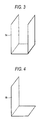
- the construction of the shielding unit 9 is not limited to those shown in Figs. 3 and 4 .
- the shielding unit 9 may be constructed otherwise into a box shape which covers a total periphery of the voltage detector 10 or into a shape having a cut in one of sides thereof, in consideration of the suppression effect of influence of radiation noise, easy fixing of itself within the device and specification with respect to limitation on the ambient temperature of the voltage detector 10.
- the power converting device for a vehicle has the configuration in which the maintenance and inspection of the equipment requiring frequent maintenance and inspection can be executed easily from the sides of the device along the traveling direction of the vehicle by disposing in the housing of the device the converter unit 2 and the inverter unit 3 on the one side along the traveling direction of the vehicle, the contactor unit 4 and the control unit 5 along the other side along the traveling direction of the vehicle, and the direct current link unit wiring 6 and other wirings and the voltage detectors 10a, 10b in the intermediate portion defined between the converter and inverter units 2, 3 and the contactor unit 4 and the control unit 5.
- the voltage detectors 10a, 10b can be disposed freely within the housing while being prevented from the influence of radiation noise from the direct current link unit wiring 6 by providing the shielding units 9 between the voltage detectors 10a, 10b and the direct current link unit wiring 6. Accordingly, it is possible to realize a reduction in size of the device by making effect use of the space within the housing.
- the disposition of the voltage detectors 10a, 10b of the embodiment 1 is not limited to that shown in Fig. 2 .
- Fig. 6 is a circuit diagram of a power converting device for a vehicle according to embodiment 2 of the invention.
- the embodiment 2 differs from the embodiment 1 in that it is applied to an electric vehicle with a two-level inverter/converter system.
- An intermediate direct current voltage has two potentials, and there is only one voltage detector 10 in this portion.
- Fig. 7 is an equipment block diagram of an interior of a housing of the power converting device according to the embodiment 2 of the invention, as seen from the top thereof.
- a converter unit 2 and an inverter unit 3, and a contactor unit 4 and a control unit 5 are disposed on both sides of an interior of a housing of a power converting device 1 along a traveling direction of the vehicle.
- a direct current link unit wiring 6 between the converter unit 2 and the inverter unit 3 and a motor wiring 7, an alternating current input wiring 8 and a voltage detector 10 are disposed in a space defined near a center of the housing between the converter unit 2 and the inverter unit 3, and the contactor unit 4 and the control unit 5.
- This voltage detector 10 is fixed to a box frame support beam 11 which lies substantially at the center of the power converting device 1 with, for example, a bolt.
- the maintenance and inspection pf the voltage detector 10 can be executed from an access hole (not shown) provided in a bottom portion of the housing of the power converting device 1.
- the voltage detector 10 has an L-shaped shielding unit 9 which can shield the radiation noise from the direct current link unit wiring 6, so as to suppress the influence of radiation noise.
- the shape of the shielding unit 9 and the disposition of the voltage detector are not limited to those illustrated.
- Fig. 8 is a circuit diagram of a power converting device for a vehicle according to embodiment 3 of the invention.
- the embodiment 3 differs from embodiment 1 in that it is applied to an electric vehicle with a two-level inverter system which runs in a direct current feeding section.
- a direct current voltage obtained from a direct current overhead wire 30 via a pantograph or the like is connected to an input filter reactor unit 32 and an input filter condenser unit 33 via a contactor unit 31.
- the direct current voltage from the direct current power supply 30 is smoothed to be supplied to the inverter unit 3, and a harmonic current generated by a power converting operation at the inverter unit 3 suppresses the influence on the direct current power supply 30.
- the smoothed direct current voltage is converted into a three-phase alternating current which is variable in voltage and variable in frequency.
- the three-phase alternating current is outputted to an electric motor 22 to drive the electric motor 22.
- Fig. 9 is an equipment block diagram of an interior of a housing of the power converting device according to the embodiment 3 of the invention, as seen from the top thereof.
- a direct current bus wiring 33 between the input filter condenser 33 and a control unit 5 and a motor wiring 7 and a voltage detector 10 are disposed in a space defined near a center of the housing between the input filter condenser 33 and the control unit 5.
- This voltage detector 10 is fixed to a box frame support beam 11 which lies substantially at the center of the power converting device 1 with a bolt or the like.
- the maintenance and inspection of the voltage detector 10 can be executed from an access hole (not shown) provided in a bottom portion of the housing of the power converting device 1.
- the inverter unit 3, the input filter condenser 33 and the control unit 5 respectively include access holes 13b, 13c, 13e which are provided to the housing, so as to facilitate the maintenance and inspections thereof from a lateral direction of the vehicle so as to facilitate the maintenance and inspections thereof from a lateral direction of the vehicle.
- the voltage detector 10 has an L-shaped shielding unit 9 which can shield the radiation noise from the direct current bus wiring 34, so as to suppress the influence of radiation noise from a main circuit wiring (here, the direct current bus wiring 34).
- the shape of the shielding unit 9 and the disposition of the voltage detector 10 are not limited to those illustrated.
- the converter unit 2, the inverter unit 3, the contactor unit 4, the control unit 5 and the input filter condenser unit 33 which require frequent maintenance and inspections, are disposed on both sides of the interior of the housing of the power converting device along the traveling direction of the vehicle, and the respective wirings and the voltage detector or detectors 10 are disposed in the space defined near the center of the housing between those constituent components. Accordingly, the power converting device is configured such that the constituent components can easily be subjected to maintenance and inspection from the sides of the vehicle.
- the influence of radiation noise is suppressed by providing the shielding unit 9 between the voltage detector 10 and the main circuit wiring, whereby the voltage detector 10 can freely be disposed in the interior of the housing of the power converting device. Accordingly, a reduction in size of the power converting device is realized by making effective use of the space within the housing.
- the voltage detector or detectors 10 are disposed in the space defined at the center of the housing, the other sensors can also be disposed similarly. Accordingly, there is an advantage that the components can be freely be disposed, so as to realize reduction in size in response to various design requirements.
Landscapes
- Engineering & Computer Science (AREA)
- Transportation (AREA)
- Mechanical Engineering (AREA)
- Power Engineering (AREA)
- Life Sciences & Earth Sciences (AREA)
- Sustainable Development (AREA)
- Sustainable Energy (AREA)
- Automation & Control Theory (AREA)
- Electric Propulsion And Braking For Vehicles (AREA)
- Inverter Devices (AREA)
Abstract
Description
- The present invention relates to a power converting device for a vehicle, which employs a power semiconductor element, and particularly, which is disposed under a floor of a railway vehicle.
- A power converting device for a vehicle includes power converting units which employ power semiconductor elements such as a so-called converter and inverter, a filter condenser and a control unit, and various types of control power supplies and sensors therefor. Equipments are disposed highly densely within a power converting device of, particularly, a high-speed railway vehicle (refer to Patent Document 1).
-
- Patent Document 1 :
JP-A-2009-96318 - In particular, in a power converting device for a railway vehicle, higher-speed and higher capacity is achieved, On the other hand, a power converting device is installed in a limited space under a floor of a vehicle, which demands a smaller power converting device. In addition, there is a problem to be solved that maintenance and inspection work has to be carried out easily while highly densely disposing the equipments in an interior of such a power converting device for a vehicle.
- Accordingly, an object of the invention is to provide a power converting device for a vehicle, which facilitates the execution of maintenance and inspection work and meets the demand for a smaller power converting device for a vehicle.
- A control device for a vehicle according to the invention includes, in a housing that is installed under a floor of the vehicle: a power converter configured of a semiconductor switching circuit; a control unit that controls the output of the power converter so as to supply a required load to a power; a main circuit wiring that is inputted to the power converter; a voltage detector that detects a voltage applied to the main circuit wiring and outputs the detected voltage to the control unit; and a shielding unit that shields radiation noise from the main circuit wiring to the voltage detector, characterized in that, the power converter and the control unit are disposed individually on both sides of the housing along a traveling direction of the vehicle, and the voltage detector is disposed between the power converter and the control unit.
- According to the power converting device for a vehicle of the invention, by disposing equipment which needs frequent maintenance and inspection work on lateral sides of an interior of the power converting device, the power converting device for a vehicle, which is small in size and which facilitates the maintenance and inspection work, can be provided.
-
-
Fig. 1 is a circuit diagram of a power converting device for a vehicle according toembodiment 1 of the invention. -
Fig. 2 is an equipment block diagram of an interior of a housing of the power converting device for a vehicle according to theembodiment 1 of the invention, as seen from the top thereof. -
Fig. 3 is a diagram showing a configuration of a shielding unit according to theembodiment 1 of the invention. -
Fig. 4 is a diagram showing another configuration of the shielding unit according to theembodiment 1 of the invention. -
Fig. 5 is another equipment block diagram of the interior of the housing of the power converting device for a vehicle according to theembodiment 1 of the invention, as seen from the top thereof. -
Fig. 6 is a circuit diagram of a power converting device for a vehicle according toembodiment 2 of the invention. -
Fig. 7 is an equipment block diagram of an interior of a housing of the power converting device according to theembodiment 2 of the invention, as seen from the top thereof. -
Fig. 8 is a circuit diagram of a power converting device for a vehicle according toembodiment 3 of the invention. -
Fig. 9 is an equipment block diagram of an interior of a housing of the power converting device according to theembodiment 3 of the invention, as seen from the top thereof. - 1 Power converting system; 2 Converter unit; 3 Inverter unit; 4 Contactor unit; 5 Control unit; 6 Direct current link unit wiring; 7 Motor wiring; 8 Alternating current input wiring; 9, 9a, 9b Shielding unit; 10, 10a, 10b Voltage detector; 11 Box frame support beam; 13a to 13e Access hole; 20 Alternating current overhead wire; 21 Transformer; 22 Electric motor; 30 Direct current overhead wire; 31 Contactor unit; 32 Input filter reactor; 33 Input filter condenser unit; 34 Direct current bus wiring; 40, 40a, 40b, Filter condenser; 42 Converter current detector; 43,
43a 43b Inverter current detector; 44 Alternating current voltage detector, - Hereinafter, the invention will be described in detail based on the drawings showing embodiments thereof.
-
Fig. 1 is a circuit diagram of a power converting device for a vehicle according toembodiment 1 of the invention. This embodiment describes an electric vehicle with a three-level inverter/converter system, which runs an alternating current feeding section. In the electric vehicle, an alternating current voltage which is obtained from an alternatingcurrent overhead wire 20 via a pantograph is once inputted into atransformer 21 for transformation to a voltage suitable for input into apower converting device 1. The voltage which is so transformed is inputted into aconverter unit 2, which is a power converter configured of a semiconductor switching circuit, via acontactor unit 4. A contactor which electrically separates theconverter unit 2 from thetransformer 21 is inserted into thecontactor unit 4, and this contactor is opened when the power converting device is not in operation or the power converting device is separated from an alternating current power supply due to the occurrence of an abnormality. - In the
converter unit 2, the alternating current input is converted into an intermediate direct current voltage, which is then outputted to filter condensers 40 (40a, 40b). In the case of a three-level converter, the intermediate direct current voltage has three potentials and is separated and smoothed by the twofilter condensers inverter unit 3, which is a power converter made up of a semiconductor switching circuit, and this intermediate direct current voltage is converted into a three-phase alternating current voltage which is variable in voltage and variable in frequency. The three-phase alternating current voltage is outputted to theelectric motor 22, whereby theelectric motor 22 is driven. - Next, a power converting operation at the
converter unit 2 will be described. Current information obtained by a convertercurrent detector 42 provided on an input line of theconverter unit 2 and voltage information obtained by an alternatingcurrent voltage detector 44 connected to one of winding outputs of thetransformer 21 are inputted into thecontrol unit 5. Similarly, voltage information obtained by voltage detectors 10 (10a, 10b), which are connected between terminals of thefilter condensers control unit 5. A converter gate signal calculated based on these pieces of information is outputted to theconverter unit 2, whereby the power converting operation from the alternating current voltage to the intermediate direct current is controlled. - On the other hand, a power converting operation at the
inverter unit 3 is executed as follows. Current information obtained by invertercurrent detectors inverter unit 3, voltage information of an intermediate direct current portion obtained by thevoltage detectors inverter unit 3, whereby the power converting operation from the intermediate direct current to the alternating current voltage, which is variable in voltage and variable in frequency, is controlled. - As has been described heretofore, various types of equipments are installed in the
power converting device 1, and the capacities of the equipments are getting larger, while the equipments need to be installed in a limited space under the floor of the vehicle. An equipment arrangement according to this embodiment, which realizes a reduction in size while taking the handy maintenance into consideration, will be described by use ofFig. 2 . -
Fig. 2 is an equipment block diagram of an interior of a housing of the power converting device for avehicle 1 according to the embodiment of the invention, as seen from the top thereof. In the interior of the housing of thepower converting device 1, theconverter unit 2 and theinverter unit 3 are disposed on one side along a traveling direction of the vehicle, and thecontactor unit 4 and thecontrol unit 5 are disposed on another side along the traveling direction of the vehicle. Due to the necessity of executing maintenance and inspections frequently, theconverter unit 2, theinverter unit 3, thecontactor unit 4 and thecontrol unit 5 respectively includeaccess holes 13a to 13d which are provided to the housing, so as to facilitate the maintenance and inspections thereof from a lateral direction of the vehicle. - In many cases, sensors such as the
converter current detector 42, theinverter current detectors alternating current detector 44 and thevoltage detectors control unit 5. However, these sensors are less frequently maintained and inspected, and hence, by disposing only sensors requiring frequent maintenance and inspections in the interior of thecontrol unit 5, thecontrol unit 5 can be reduced in size. - In particular, in consideration of the influence of radiation noise by a high-frequency power generated from switching circuits of the
converter unit 2 and theinverter unit 3 which are power converters, thevoltage detectors 10 needs to be disposed separately in a position which is spaced away from a main circuit wiring (here, a direct current link unit wiring 6) and other wirings which emit radiation noise (in the control unit, for example). Thus, thevoltage detectors 10 do not have much degree of freedom in arrangement, which made it difficult to realize a reduction in size of the power converting device in whole. - In this application, however, by disposing
shielding units 9 which include a metal such as aluminum between the direct currentlink unit wiring 6 and the voltage detectors 10 (10a, 10b), where the radiation noise is generated the most, the influence of the radiation noise can be suppressed, and therefore, thevoltage detectors 10 can be disposed freely within the housing. - Consequently, the direct current
link unit wiring 6 between theconverter unit 2 and theinverter unit 3, amotor wiring 7, an alternatingcurrent input wiring 8 and thevoltage detectors converter unit 2 and theinverter unit 3, and thecontactor unit 4 and thecontrol unit 5 which are disposed on both the sides of the housing along the traveling direction of the vehicle. Thevoltage detectors frame support beam 11 which lies substantially at the center of thepower converting device 1 with a bolt or the like. The maintenance and inspection of thevoltage detectors power converting device 1. -
Figs. 3 and 4 show examples ofshielding units 9.Shielding units 9 are each made up of a plate containing a metal which includes a surface or surfaces each having an area capable of shielding thecorresponding voltage detector 10 from radiation noise from the direct currentlink unit wiring 6 in accordance with a place where thevoltage detector 10 is disposed and a surface on which theshielding unit 9 is fixed to the boxframe support beam 11 with a bolt or the like. - NeedJess to say, the construction of the
shielding unit 9 is not limited to those shown inFigs. 3 and 4 . Theshielding unit 9 may be constructed otherwise into a box shape which covers a total periphery of thevoltage detector 10 or into a shape having a cut in one of sides thereof, in consideration of the suppression effect of influence of radiation noise, easy fixing of itself within the device and specification with respect to limitation on the ambient temperature of thevoltage detector 10. - Thus, as has been described above, the power converting device for a vehicle according to the
embodiment 1 has the configuration in which the maintenance and inspection of the equipment requiring frequent maintenance and inspection can be executed easily from the sides of the device along the traveling direction of the vehicle by disposing in the housing of the device theconverter unit 2 and theinverter unit 3 on the one side along the traveling direction of the vehicle, thecontactor unit 4 and thecontrol unit 5 along the other side along the traveling direction of the vehicle, and the direct currentlink unit wiring 6 and other wirings and thevoltage detectors inverter units contactor unit 4 and thecontrol unit 5. - Further, the
voltage detectors link unit wiring 6 by providing theshielding units 9 between thevoltage detectors link unit wiring 6. Accordingly, it is possible to realize a reduction in size of the device by making effect use of the space within the housing. - The disposition of the
voltage detectors embodiment 1 is not limited to that shown inFig. 2 . For example, it is possible to realize a further reduction in size in a width direction of the vehicle by adopting a disposition shown inFig. 5 . -
Fig. 6 is a circuit diagram of a power converting device for a vehicle according toembodiment 2 of the invention. Theembodiment 2 differs from theembodiment 1 in that it is applied to an electric vehicle with a two-level inverter/converter system. An intermediate direct current voltage has two potentials, and there is only onevoltage detector 10 in this portion. -
Fig. 7 is an equipment block diagram of an interior of a housing of the power converting device according to theembodiment 2 of the invention, as seen from the top thereof. Aconverter unit 2 and aninverter unit 3, and acontactor unit 4 and acontrol unit 5 are disposed on both sides of an interior of a housing of apower converting device 1 along a traveling direction of the vehicle. In addition, a direct currentlink unit wiring 6 between theconverter unit 2 and theinverter unit 3 and amotor wiring 7, an alternatingcurrent input wiring 8 and avoltage detector 10 are disposed in a space defined near a center of the housing between theconverter unit 2 and theinverter unit 3, and thecontactor unit 4 and thecontrol unit 5. Thisvoltage detector 10 is fixed to a boxframe support beam 11 which lies substantially at the center of thepower converting device 1 with, for example, a bolt. The maintenance and inspection pf thevoltage detector 10 can be executed from an access hole (not shown) provided in a bottom portion of the housing of thepower converting device 1. - The
voltage detector 10 has an L-shapedshielding unit 9 which can shield the radiation noise from the direct currentlink unit wiring 6, so as to suppress the influence of radiation noise. The shape of theshielding unit 9 and the disposition of the voltage detector are not limited to those illustrated. -
Fig. 8 is a circuit diagram of a power converting device for a vehicle according toembodiment 3 of the invention. Theembodiment 3 differs fromembodiment 1 in that it is applied to an electric vehicle with a two-level inverter system which runs in a direct current feeding section. A direct current voltage obtained from a direct currentoverhead wire 30 via a pantograph or the like is connected to an inputfilter reactor unit 32 and an inputfilter condenser unit 33 via acontactor unit 31. - Accordingly, the direct current voltage from the direct
current power supply 30 is smoothed to be supplied to theinverter unit 3, and a harmonic current generated by a power converting operation at theinverter unit 3 suppresses the influence on the directcurrent power supply 30. At theinverter unit 3, the smoothed direct current voltage is converted into a three-phase alternating current which is variable in voltage and variable in frequency. The three-phase alternating current is outputted to anelectric motor 22 to drive theelectric motor 22. -
Fig. 9 is an equipment block diagram of an interior of a housing of the power converting device according to theembodiment 3 of the invention, as seen from the top thereof. A directcurrent bus wiring 33 between theinput filter condenser 33 and acontrol unit 5 and amotor wiring 7 and avoltage detector 10 are disposed in a space defined near a center of the housing between theinput filter condenser 33 and thecontrol unit 5. Thisvoltage detector 10 is fixed to a boxframe support beam 11 which lies substantially at the center of thepower converting device 1 with a bolt or the like. The maintenance and inspection of thevoltage detector 10 can be executed from an access hole (not shown) provided in a bottom portion of the housing of thepower converting device 1. - Due to the necessity of executing maintenance and inspections frequently, the
inverter unit 3, theinput filter condenser 33 and thecontrol unit 5 respectively includeaccess holes - The
voltage detector 10 has an L-shapedshielding unit 9 which can shield the radiation noise from the directcurrent bus wiring 34, so as to suppress the influence of radiation noise from a main circuit wiring (here, the direct current bus wiring 34). The shape of theshielding unit 9 and the disposition of thevoltage detector 10 are not limited to those illustrated. - As described above, in the embodiments of this application, the
converter unit 2, theinverter unit 3, thecontactor unit 4, thecontrol unit 5 and the inputfilter condenser unit 33 ,which require frequent maintenance and inspections, are disposed on both sides of the interior of the housing of the power converting device along the traveling direction of the vehicle, and the respective wirings and the voltage detector ordetectors 10 are disposed in the space defined near the center of the housing between those constituent components. Accordingly, the power converting device is configured such that the constituent components can easily be subjected to maintenance and inspection from the sides of the vehicle. - Further, the influence of radiation noise is suppressed by providing the
shielding unit 9 between thevoltage detector 10 and the main circuit wiring, whereby thevoltage detector 10 can freely be disposed in the interior of the housing of the power converting device. Accordingly, a reduction in size of the power converting device is realized by making effective use of the space within the housing. - In the embodiments described above, while the voltage detector or
detectors 10 are disposed in the space defined at the center of the housing, the other sensors can also be disposed similarly. Accordingly, there is an advantage that the components can be freely be disposed, so as to realize reduction in size in response to various design requirements.
Claims (7)
- A control device for a vehicle, the control device comprising, in a housing that is installed under a floor of the vehicle:a power converter configured of a semiconductor switching circuit;a control unit that controls the output of the power converter so as to supply a required load to a power;a main circuit wiring that is inputted to the power converter;a voltage detector that detects a voltage applied to the main circuit wiring and outputs the detected voltage to the control unit; anda shielding unit that shields radiation noise from the main circuit wiring to the voltage detector,characterized in that,the power converter and the control unit are disposed individually on both sides of the housing along a traveling direction of the vehicle, and the voltage detector is disposed between the power converter and the control unit.
- A control device for a vehicle according to claim 1, characterized in that
the control unit that includes a first access hole and a contactor unit that includes a second access hole are disposed at one side of the housing along the traveling direction of the vehicle, and
the power converter that includes a third access hole is disposed at another side of the housing along the traveling direction of the vehicle. - A control device for a vehicle according to claim 1, characterized in that
the control unit that includes a first access hole and an input filter condenser unit that includes a second access hole are disposed at one side of the housing along the traveling direction of the vehicle, and
the power converter that includes a third access hole is disposed at another side of the housing along the traveling direction of the vehicle. - A control device for a vehicle according to claim 1, characterized in that
the power converter is configured of an inverter unit and a converter unit,
the control unit that includes a first access hole and a contactor unit that includes a second access hole are disposed at one side of the housing along the traveling direction of the vehicle, and
the inverter unit that includes a third access hole and the converter unit that includes a fourth access hole are disposed at another side of the housing along the traveling direction of the vehicle. - A control device for a vehicle according to claim 1, characterized in that
a plurality of the voltage detectors each has a shielding unit and are disposed so as to be aligned in a direction perpendicular to the traveling direction of the vehicle. - A control device for a vehicle according to claim 1, characterized in that
a plurality of the voltage detectors each has a shielding unit and are disposed so as to be aligned in a direction parallel to the traveling direction of the vehicle. - A control device for a vehicle according to claim 1, characterized in that
the shielding unit is configured of a plate containing metal, which includes a surface having a surface area capable of shielding radiation noise from the main circuit wiring.
Applications Claiming Priority (1)
| Application Number | Priority Date | Filing Date | Title |
|---|---|---|---|
| PCT/JP2009/002668 WO2010143236A1 (en) | 2009-06-12 | 2009-06-12 | Electric power conversion device for vehicle |
Publications (3)
| Publication Number | Publication Date |
|---|---|
| EP2441639A1 true EP2441639A1 (en) | 2012-04-18 |
| EP2441639A4 EP2441639A4 (en) | 2013-10-30 |
| EP2441639B1 EP2441639B1 (en) | 2015-05-20 |
Family
ID=43308508
Family Applications (1)
| Application Number | Title | Priority Date | Filing Date |
|---|---|---|---|
| EP09845761.7A Not-in-force EP2441639B1 (en) | 2009-06-12 | 2009-06-12 | Electric power conversion device for vehicle |
Country Status (12)
| Country | Link |
|---|---|
| US (1) | US9694689B2 (en) |
| EP (1) | EP2441639B1 (en) |
| JP (1) | JP4614020B1 (en) |
| KR (1) | KR101320167B1 (en) |
| CN (1) | CN102574532B (en) |
| AU (1) | AU2009347792B2 (en) |
| BR (1) | BRPI0924550A2 (en) |
| CA (1) | CA2765346C (en) |
| MX (1) | MX2011013329A (en) |
| RU (1) | RU2494898C2 (en) |
| WO (1) | WO2010143236A1 (en) |
| ZA (1) | ZA201108985B (en) |
Cited By (3)
| Publication number | Priority date | Publication date | Assignee | Title |
|---|---|---|---|---|
| CN103373240A (en) * | 2012-04-26 | 2013-10-30 | 本田技研工业株式会社 | Power control unit |
| CN106655717A (en) * | 2016-11-16 | 2017-05-10 | 国网山东省电力公司栖霞市供电公司 | Low-noise power converter |
| EP3228490B1 (en) | 2016-03-30 | 2019-12-18 | Hitachi, Ltd. | Power conversion device |
Families Citing this family (8)
| Publication number | Priority date | Publication date | Assignee | Title |
|---|---|---|---|---|
| JP5214065B1 (en) * | 2012-01-30 | 2013-06-19 | 三菱電機株式会社 | Electric car main circuit system |
| JP6602633B2 (en) * | 2015-10-13 | 2019-11-06 | 株式会社東芝 | Power converter |
| IT201700070324A1 (en) * | 2017-06-23 | 2018-12-23 | Meta System Spa | ELECTRONIC POWER EQUIPMENT FOR ELECTRIC OR HYBRID CARS AND ITS APPLICATION PROCEDURE |
| US11433928B2 (en) * | 2017-10-27 | 2022-09-06 | Mitsubishi Electric Corporation | Underfloor device for railway vehicle |
| JP7117907B2 (en) * | 2018-06-18 | 2022-08-15 | 株式会社日立製作所 | Condition monitoring device and transportation vehicle equipped with it |
| EP3696007B1 (en) | 2019-02-18 | 2021-10-06 | Bombardier Transportation GmbH | An arrangement for earthing a dc intermediate link |
| JP7530358B2 (en) | 2019-07-04 | 2024-08-07 | 三菱電機株式会社 | Electric vehicle drive system and electric vehicle control device protection method |
| JP7204623B2 (en) * | 2019-09-20 | 2023-01-16 | 日立Astemo株式会社 | Electromechanical Integrated Power Conversion Device and Drive Device for Electric Vehicle |
Family Cites Families (21)
| Publication number | Priority date | Publication date | Assignee | Title |
|---|---|---|---|---|
| JPS5574204U (en) * | 1978-11-17 | 1980-05-22 | ||
| JPS58211962A (en) * | 1982-06-02 | 1983-12-09 | 株式会社日立製作所 | Controller for car |
| JPS63283401A (en) | 1987-05-15 | 1988-11-21 | Hitachi Ltd | Inverter for vehicle |
| JPH01135798U (en) | 1988-03-09 | 1989-09-18 | ||
| JPH08238950A (en) * | 1995-03-07 | 1996-09-17 | Toshiba Corp | Vehicle semiconductor control device |
| US5687066A (en) * | 1995-04-06 | 1997-11-11 | Progressive Dynamics, Inc. | Power converter with overvoltage protection |
| JPH0937414A (en) | 1995-07-20 | 1997-02-07 | Mitsubishi Electric Corp | Inverter device for electric vehicles |
| JP3843422B2 (en) * | 1998-09-30 | 2006-11-08 | 株式会社日立製作所 | Power converter |
| DE19849858A1 (en) | 1998-10-29 | 2000-05-04 | Abb Daimler Benz Transp | Capacitor assembly for a converter device |
| JP3747255B2 (en) * | 1999-04-23 | 2006-02-22 | 株式会社日立製作所 | Electric vehicle control device |
| JP3643514B2 (en) * | 2000-03-10 | 2005-04-27 | 株式会社東芝 | Railway vehicle power converter |
| WO2003088728A1 (en) | 2002-04-12 | 2003-10-23 | Bombardier Transportation Gmbh | Power converter module |
| JP2005229708A (en) * | 2004-02-12 | 2005-08-25 | Toshiba Corp | Railway vehicle power converter |
| JP4455145B2 (en) * | 2004-04-27 | 2010-04-21 | 株式会社東芝 | Railway vehicle drive control device |
| RU50060U1 (en) * | 2005-06-07 | 2005-12-10 | Яцук Владимир Григорьевич | HIGH VOLTAGE STATIC CONVERTER FOR PASSENGER CAR |
| US7808195B2 (en) * | 2006-05-15 | 2010-10-05 | Mitsubishi Electric Corporation | Control apparatus for electric train |
| JPWO2007138645A1 (en) * | 2006-05-25 | 2009-10-01 | 三菱電機株式会社 | Auxiliary power supply for vehicle |
| JP4987495B2 (en) * | 2007-01-25 | 2012-07-25 | 株式会社東芝 | Motor drive system for rail car drive |
| JP4457121B2 (en) | 2007-03-28 | 2010-04-28 | 日立オートモティブシステムズ株式会社 | Electric brake device |
| JP5148238B2 (en) * | 2007-10-16 | 2013-02-20 | 東海旅客鉄道株式会社 | High-speed railway vehicle power converter |
| JP5558022B2 (en) * | 2009-04-15 | 2014-07-23 | 株式会社東芝 | Electric vehicle storage control device and storage control method |
-
2009
- 2009-06-12 KR KR1020117029736A patent/KR101320167B1/en not_active Expired - Fee Related
- 2009-06-12 RU RU2012100770/11A patent/RU2494898C2/en not_active IP Right Cessation
- 2009-06-12 WO PCT/JP2009/002668 patent/WO2010143236A1/en not_active Ceased
- 2009-06-12 EP EP09845761.7A patent/EP2441639B1/en not_active Not-in-force
- 2009-06-12 US US13/322,253 patent/US9694689B2/en not_active Expired - Fee Related
- 2009-06-12 MX MX2011013329A patent/MX2011013329A/en active IP Right Grant
- 2009-06-12 AU AU2009347792A patent/AU2009347792B2/en not_active Ceased
- 2009-06-12 JP JP2010530792A patent/JP4614020B1/en not_active Expired - Fee Related
- 2009-06-12 BR BRPI0924550-2A patent/BRPI0924550A2/en not_active Application Discontinuation
- 2009-06-12 CA CA2765346A patent/CA2765346C/en not_active Expired - Fee Related
- 2009-06-12 CN CN200980159982.6A patent/CN102574532B/en not_active Expired - Fee Related
-
2011
- 2011-12-07 ZA ZA2011/08985A patent/ZA201108985B/en unknown
Cited By (4)
| Publication number | Priority date | Publication date | Assignee | Title |
|---|---|---|---|---|
| CN103373240A (en) * | 2012-04-26 | 2013-10-30 | 本田技研工业株式会社 | Power control unit |
| EP3228490B1 (en) | 2016-03-30 | 2019-12-18 | Hitachi, Ltd. | Power conversion device |
| EP3228490B2 (en) † | 2016-03-30 | 2025-01-15 | Hitachi, Ltd. | Power conversion device |
| CN106655717A (en) * | 2016-11-16 | 2017-05-10 | 国网山东省电力公司栖霞市供电公司 | Low-noise power converter |
Also Published As
| Publication number | Publication date |
|---|---|
| AU2009347792A1 (en) | 2012-01-19 |
| CN102574532B (en) | 2016-01-20 |
| KR20120012832A (en) | 2012-02-10 |
| CA2765346C (en) | 2014-01-21 |
| RU2494898C2 (en) | 2013-10-10 |
| RU2012100770A (en) | 2013-07-20 |
| US9694689B2 (en) | 2017-07-04 |
| WO2010143236A1 (en) | 2010-12-16 |
| JP4614020B1 (en) | 2011-01-19 |
| JPWO2010143236A1 (en) | 2012-11-22 |
| CA2765346A1 (en) | 2010-12-16 |
| BRPI0924550A2 (en) | 2015-06-30 |
| AU2009347792B2 (en) | 2015-04-23 |
| EP2441639A4 (en) | 2013-10-30 |
| EP2441639B1 (en) | 2015-05-20 |
| CN102574532A (en) | 2012-07-11 |
| KR101320167B1 (en) | 2013-10-23 |
| US20120063176A1 (en) | 2012-03-15 |
| MX2011013329A (en) | 2012-06-08 |
| ZA201108985B (en) | 2013-02-27 |
Similar Documents
| Publication | Publication Date | Title |
|---|---|---|
| EP2441639B1 (en) | Electric power conversion device for vehicle | |
| RU2471656C1 (en) | Automotive control device | |
| US9776514B2 (en) | DC-DC converter | |
| EP2264883B1 (en) | Power converter for railway rolling stock | |
| US9925880B2 (en) | Vehicle with power electronics | |
| JP5437314B2 (en) | Power converter | |
| JP2009105178A (en) | Power semiconductor unit | |
| US8493731B2 (en) | Forced-air-cooled vehicle control device | |
| JP2012253857A (en) | Power conversion device | |
| JP7107521B2 (en) | Inverter controller | |
| JP2012253856A (en) | Power conversion device | |
| JP5560232B2 (en) | Current detector | |
| WO2019026369A1 (en) | Inverter device | |
| JP5381076B2 (en) | Power converter | |
| CN105122616A (en) | Crane device, container yard and power supply method | |
| JP7369640B2 (en) | Auxiliary power supply | |
| JP2017212333A (en) | Board support bracket | |
| JP5413030B2 (en) | Power converter |
Legal Events
| Date | Code | Title | Description |
|---|---|---|---|
| PUAI | Public reference made under article 153(3) epc to a published international application that has entered the european phase |
Free format text: ORIGINAL CODE: 0009012 |
|
| 17P | Request for examination filed |
Effective date: 20111212 |
|
| AK | Designated contracting states |
Kind code of ref document: A1 Designated state(s): AT BE BG CH CY CZ DE DK EE ES FI FR GB GR HR HU IE IS IT LI LT LU LV MC MK MT NL NO PL PT RO SE SI SK TR |
|
| DAX | Request for extension of the european patent (deleted) | ||
| A4 | Supplementary search report drawn up and despatched |
Effective date: 20131001 |
|
| RIC1 | Information provided on ipc code assigned before grant |
Ipc: H02M 7/00 20060101ALI20130925BHEP Ipc: B60L 9/16 20060101ALI20130925BHEP Ipc: B60L 15/00 20060101ALI20130925BHEP Ipc: H01L 23/00 20060101ALI20130925BHEP Ipc: H02K 5/24 20060101ALI20130925BHEP Ipc: B61C 17/12 20060101AFI20130925BHEP |
|
| RIC1 | Information provided on ipc code assigned before grant |
Ipc: H01L 23/00 20060101ALI20140902BHEP Ipc: H02K 5/24 20060101ALI20140902BHEP Ipc: H02M 7/00 20060101ALI20140902BHEP Ipc: B60L 9/16 20060101ALI20140902BHEP Ipc: B60L 15/00 20060101ALI20140902BHEP Ipc: B61C 17/12 20060101AFI20140902BHEP |
|
| GRAP | Despatch of communication of intention to grant a patent |
Free format text: ORIGINAL CODE: EPIDOSNIGR1 |
|
| INTG | Intention to grant announced |
Effective date: 20141202 |
|
| GRAS | Grant fee paid |
Free format text: ORIGINAL CODE: EPIDOSNIGR3 |
|
| GRAA | (expected) grant |
Free format text: ORIGINAL CODE: 0009210 |
|
| AK | Designated contracting states |
Kind code of ref document: B1 Designated state(s): AT BE BG CH CY CZ DE DK EE ES FI FR GB GR HR HU IE IS IT LI LT LU LV MC MK MT NL NO PL PT RO SE SI SK TR |
|
| REG | Reference to a national code |
Ref country code: GB Ref legal event code: FG4D |
|
| REG | Reference to a national code |
Ref country code: CH Ref legal event code: EP |
|
| REG | Reference to a national code |
Ref country code: AT Ref legal event code: REF Ref document number: 727595 Country of ref document: AT Kind code of ref document: T Effective date: 20150615 |
|
| REG | Reference to a national code |
Ref country code: IE Ref legal event code: FG4D |
|
| REG | Reference to a national code |
Ref country code: DE Ref legal event code: R096 Ref document number: 602009031376 Country of ref document: DE Effective date: 20150625 |
|
| REG | Reference to a national code |
Ref country code: AT Ref legal event code: MK05 Ref document number: 727595 Country of ref document: AT Kind code of ref document: T Effective date: 20150520 |
|
| REG | Reference to a national code |
Ref country code: LT Ref legal event code: MG4D |
|
| REG | Reference to a national code |
Ref country code: NL Ref legal event code: MP Effective date: 20150520 |
|
| PG25 | Lapsed in a contracting state [announced via postgrant information from national office to epo] |
Ref country code: FI Free format text: LAPSE BECAUSE OF FAILURE TO SUBMIT A TRANSLATION OF THE DESCRIPTION OR TO PAY THE FEE WITHIN THE PRESCRIBED TIME-LIMIT Effective date: 20150520 Ref country code: NO Free format text: LAPSE BECAUSE OF FAILURE TO SUBMIT A TRANSLATION OF THE DESCRIPTION OR TO PAY THE FEE WITHIN THE PRESCRIBED TIME-LIMIT Effective date: 20150820 Ref country code: PT Free format text: LAPSE BECAUSE OF FAILURE TO SUBMIT A TRANSLATION OF THE DESCRIPTION OR TO PAY THE FEE WITHIN THE PRESCRIBED TIME-LIMIT Effective date: 20150921 Ref country code: HR Free format text: LAPSE BECAUSE OF FAILURE TO SUBMIT A TRANSLATION OF THE DESCRIPTION OR TO PAY THE FEE WITHIN THE PRESCRIBED TIME-LIMIT Effective date: 20150520 Ref country code: ES Free format text: LAPSE BECAUSE OF FAILURE TO SUBMIT A TRANSLATION OF THE DESCRIPTION OR TO PAY THE FEE WITHIN THE PRESCRIBED TIME-LIMIT Effective date: 20150520 Ref country code: LT Free format text: LAPSE BECAUSE OF FAILURE TO SUBMIT A TRANSLATION OF THE DESCRIPTION OR TO PAY THE FEE WITHIN THE PRESCRIBED TIME-LIMIT Effective date: 20150520 |
|
| PG25 | Lapsed in a contracting state [announced via postgrant information from national office to epo] |
Ref country code: LV Free format text: LAPSE BECAUSE OF FAILURE TO SUBMIT A TRANSLATION OF THE DESCRIPTION OR TO PAY THE FEE WITHIN THE PRESCRIBED TIME-LIMIT Effective date: 20150520 Ref country code: GR Free format text: LAPSE BECAUSE OF FAILURE TO SUBMIT A TRANSLATION OF THE DESCRIPTION OR TO PAY THE FEE WITHIN THE PRESCRIBED TIME-LIMIT Effective date: 20150821 Ref country code: IS Free format text: LAPSE BECAUSE OF FAILURE TO SUBMIT A TRANSLATION OF THE DESCRIPTION OR TO PAY THE FEE WITHIN THE PRESCRIBED TIME-LIMIT Effective date: 20150920 Ref country code: AT Free format text: LAPSE BECAUSE OF FAILURE TO SUBMIT A TRANSLATION OF THE DESCRIPTION OR TO PAY THE FEE WITHIN THE PRESCRIBED TIME-LIMIT Effective date: 20150520 Ref country code: BG Free format text: LAPSE BECAUSE OF FAILURE TO SUBMIT A TRANSLATION OF THE DESCRIPTION OR TO PAY THE FEE WITHIN THE PRESCRIBED TIME-LIMIT Effective date: 20150820 |
|
| PG25 | Lapsed in a contracting state [announced via postgrant information from national office to epo] |
Ref country code: EE Free format text: LAPSE BECAUSE OF FAILURE TO SUBMIT A TRANSLATION OF THE DESCRIPTION OR TO PAY THE FEE WITHIN THE PRESCRIBED TIME-LIMIT Effective date: 20150520 Ref country code: DK Free format text: LAPSE BECAUSE OF FAILURE TO SUBMIT A TRANSLATION OF THE DESCRIPTION OR TO PAY THE FEE WITHIN THE PRESCRIBED TIME-LIMIT Effective date: 20150520 Ref country code: IT Free format text: LAPSE BECAUSE OF FAILURE TO SUBMIT A TRANSLATION OF THE DESCRIPTION OR TO PAY THE FEE WITHIN THE PRESCRIBED TIME-LIMIT Effective date: 20150520 |
|
| REG | Reference to a national code |
Ref country code: CH Ref legal event code: PL |
|
| REG | Reference to a national code |
Ref country code: DE Ref legal event code: R097 Ref document number: 602009031376 Country of ref document: DE |
|
| PG25 | Lapsed in a contracting state [announced via postgrant information from national office to epo] |
Ref country code: RO Free format text: LAPSE BECAUSE OF NON-PAYMENT OF DUE FEES Effective date: 20150520 Ref country code: MC Free format text: LAPSE BECAUSE OF FAILURE TO SUBMIT A TRANSLATION OF THE DESCRIPTION OR TO PAY THE FEE WITHIN THE PRESCRIBED TIME-LIMIT Effective date: 20150520 Ref country code: PL Free format text: LAPSE BECAUSE OF FAILURE TO SUBMIT A TRANSLATION OF THE DESCRIPTION OR TO PAY THE FEE WITHIN THE PRESCRIBED TIME-LIMIT Effective date: 20150520 Ref country code: SK Free format text: LAPSE BECAUSE OF FAILURE TO SUBMIT A TRANSLATION OF THE DESCRIPTION OR TO PAY THE FEE WITHIN THE PRESCRIBED TIME-LIMIT Effective date: 20150520 Ref country code: CZ Free format text: LAPSE BECAUSE OF FAILURE TO SUBMIT A TRANSLATION OF THE DESCRIPTION OR TO PAY THE FEE WITHIN THE PRESCRIBED TIME-LIMIT Effective date: 20150520 |
|
| REG | Reference to a national code |
Ref country code: IE Ref legal event code: MM4A |
|
| PLBE | No opposition filed within time limit |
Free format text: ORIGINAL CODE: 0009261 |
|
| STAA | Information on the status of an ep patent application or granted ep patent |
Free format text: STATUS: NO OPPOSITION FILED WITHIN TIME LIMIT |
|
| 26N | No opposition filed |
Effective date: 20160223 |
|
| PG25 | Lapsed in a contracting state [announced via postgrant information from national office to epo] |
Ref country code: CH Free format text: LAPSE BECAUSE OF NON-PAYMENT OF DUE FEES Effective date: 20150630 Ref country code: IE Free format text: LAPSE BECAUSE OF NON-PAYMENT OF DUE FEES Effective date: 20150612 Ref country code: LI Free format text: LAPSE BECAUSE OF NON-PAYMENT OF DUE FEES Effective date: 20150630 |
|
| REG | Reference to a national code |
Ref country code: FR Ref legal event code: PLFP Year of fee payment: 8 |
|
| PG25 | Lapsed in a contracting state [announced via postgrant information from national office to epo] |
Ref country code: SI Free format text: LAPSE BECAUSE OF FAILURE TO SUBMIT A TRANSLATION OF THE DESCRIPTION OR TO PAY THE FEE WITHIN THE PRESCRIBED TIME-LIMIT Effective date: 20150520 |
|
| PG25 | Lapsed in a contracting state [announced via postgrant information from national office to epo] |
Ref country code: BE Free format text: LAPSE BECAUSE OF FAILURE TO SUBMIT A TRANSLATION OF THE DESCRIPTION OR TO PAY THE FEE WITHIN THE PRESCRIBED TIME-LIMIT Effective date: 20150520 |
|
| PG25 | Lapsed in a contracting state [announced via postgrant information from national office to epo] |
Ref country code: MT Free format text: LAPSE BECAUSE OF FAILURE TO SUBMIT A TRANSLATION OF THE DESCRIPTION OR TO PAY THE FEE WITHIN THE PRESCRIBED TIME-LIMIT Effective date: 20150520 |
|
| REG | Reference to a national code |
Ref country code: DE Ref legal event code: R084 Ref document number: 602009031376 Country of ref document: DE |
|
| REG | Reference to a national code |
Ref country code: FR Ref legal event code: PLFP Year of fee payment: 9 |
|
| REG | Reference to a national code |
Ref country code: GB Ref legal event code: 746 Effective date: 20170425 |
|
| PG25 | Lapsed in a contracting state [announced via postgrant information from national office to epo] |
Ref country code: HU Free format text: LAPSE BECAUSE OF FAILURE TO SUBMIT A TRANSLATION OF THE DESCRIPTION OR TO PAY THE FEE WITHIN THE PRESCRIBED TIME-LIMIT; INVALID AB INITIO Effective date: 20090612 |
|
| PG25 | Lapsed in a contracting state [announced via postgrant information from national office to epo] |
Ref country code: SE Free format text: LAPSE BECAUSE OF FAILURE TO SUBMIT A TRANSLATION OF THE DESCRIPTION OR TO PAY THE FEE WITHIN THE PRESCRIBED TIME-LIMIT Effective date: 20150520 Ref country code: NL Free format text: LAPSE BECAUSE OF FAILURE TO SUBMIT A TRANSLATION OF THE DESCRIPTION OR TO PAY THE FEE WITHIN THE PRESCRIBED TIME-LIMIT Effective date: 20150520 Ref country code: CY Free format text: LAPSE BECAUSE OF FAILURE TO SUBMIT A TRANSLATION OF THE DESCRIPTION OR TO PAY THE FEE WITHIN THE PRESCRIBED TIME-LIMIT Effective date: 20150520 |
|
| PG25 | Lapsed in a contracting state [announced via postgrant information from national office to epo] |
Ref country code: TR Free format text: LAPSE BECAUSE OF FAILURE TO SUBMIT A TRANSLATION OF THE DESCRIPTION OR TO PAY THE FEE WITHIN THE PRESCRIBED TIME-LIMIT Effective date: 20150520 |
|
| PG25 | Lapsed in a contracting state [announced via postgrant information from national office to epo] |
Ref country code: LU Free format text: LAPSE BECAUSE OF NON-PAYMENT OF DUE FEES Effective date: 20150612 |
|
| REG | Reference to a national code |
Ref country code: FR Ref legal event code: PLFP Year of fee payment: 10 |
|
| PG25 | Lapsed in a contracting state [announced via postgrant information from national office to epo] |
Ref country code: MK Free format text: LAPSE BECAUSE OF FAILURE TO SUBMIT A TRANSLATION OF THE DESCRIPTION OR TO PAY THE FEE WITHIN THE PRESCRIBED TIME-LIMIT Effective date: 20150520 |
|
| PGFP | Annual fee paid to national office [announced via postgrant information from national office to epo] |
Ref country code: FR Payment date: 20180511 Year of fee payment: 10 |
|
| PGFP | Annual fee paid to national office [announced via postgrant information from national office to epo] |
Ref country code: GB Payment date: 20180606 Year of fee payment: 10 |
|
| GBPC | Gb: european patent ceased through non-payment of renewal fee |
Effective date: 20190612 |
|
| PG25 | Lapsed in a contracting state [announced via postgrant information from national office to epo] |
Ref country code: GB Free format text: LAPSE BECAUSE OF NON-PAYMENT OF DUE FEES Effective date: 20190612 |
|
| PG25 | Lapsed in a contracting state [announced via postgrant information from national office to epo] |
Ref country code: FR Free format text: LAPSE BECAUSE OF NON-PAYMENT OF DUE FEES Effective date: 20190630 |
|
| P01 | Opt-out of the competence of the unified patent court (upc) registered |
Effective date: 20230512 |
|
| PGFP | Annual fee paid to national office [announced via postgrant information from national office to epo] |
Ref country code: DE Payment date: 20230502 Year of fee payment: 15 |
|
| REG | Reference to a national code |
Ref country code: DE Ref legal event code: R119 Ref document number: 602009031376 Country of ref document: DE |
|
| PG25 | Lapsed in a contracting state [announced via postgrant information from national office to epo] |
Ref country code: DE Free format text: LAPSE BECAUSE OF NON-PAYMENT OF DUE FEES Effective date: 20250101 |