EP2440020B1 - Génération à partir de la sortie d'un gradateur à coupure de phase à réponse rapide à des changements dans la position du gradateur - Google Patents
Génération à partir de la sortie d'un gradateur à coupure de phase à réponse rapide à des changements dans la position du gradateur Download PDFInfo
- Publication number
- EP2440020B1 EP2440020B1 EP10186908.9A EP10186908A EP2440020B1 EP 2440020 B1 EP2440020 B1 EP 2440020B1 EP 10186908 A EP10186908 A EP 10186908A EP 2440020 B1 EP2440020 B1 EP 2440020B1
- Authority
- EP
- European Patent Office
- Prior art keywords
- period
- rate
- clock
- signal
- counter
- Prior art date
- Legal status (The legal status is an assumption and is not a legal conclusion. Google has not performed a legal analysis and makes no representation as to the accuracy of the status listed.)
- Active
Links
- 230000004044 response Effects 0.000 title claims description 22
- 238000000034 method Methods 0.000 claims description 17
- 230000000295 complement effect Effects 0.000 claims description 4
- 238000010586 diagram Methods 0.000 description 4
- 238000012545 processing Methods 0.000 description 4
- 239000003990 capacitor Substances 0.000 description 3
- 238000009966 trimming Methods 0.000 description 3
- 238000011088 calibration curve Methods 0.000 description 2
- 230000000630 rising effect Effects 0.000 description 2
- 101100537098 Mus musculus Alyref gene Proteins 0.000 description 1
- 101150095908 apex1 gene Proteins 0.000 description 1
- 238000001914 filtration Methods 0.000 description 1
- 238000012886 linear function Methods 0.000 description 1
- 238000012805 post-processing Methods 0.000 description 1
- 230000004043 responsiveness Effects 0.000 description 1
- 238000012358 sourcing Methods 0.000 description 1
- 230000001960 triggered effect Effects 0.000 description 1
Images


Classifications
-
- H—ELECTRICITY
- H05—ELECTRIC TECHNIQUES NOT OTHERWISE PROVIDED FOR
- H05B—ELECTRIC HEATING; ELECTRIC LIGHT SOURCES NOT OTHERWISE PROVIDED FOR; CIRCUIT ARRANGEMENTS FOR ELECTRIC LIGHT SOURCES, IN GENERAL
- H05B39/00—Circuit arrangements or apparatus for operating incandescent light sources
- H05B39/04—Controlling
- H05B39/08—Controlling by shifting phase of trigger voltage applied to gas-filled controlling tubes also in controlled semiconductor devices
-
- H—ELECTRICITY
- H05—ELECTRIC TECHNIQUES NOT OTHERWISE PROVIDED FOR
- H05B—ELECTRIC HEATING; ELECTRIC LIGHT SOURCES NOT OTHERWISE PROVIDED FOR; CIRCUIT ARRANGEMENTS FOR ELECTRIC LIGHT SOURCES, IN GENERAL
- H05B47/00—Circuit arrangements for operating light sources in general, i.e. where the type of light source is not relevant
- H05B47/10—Controlling the light source
-
- Y—GENERAL TAGGING OF NEW TECHNOLOGICAL DEVELOPMENTS; GENERAL TAGGING OF CROSS-SECTIONAL TECHNOLOGIES SPANNING OVER SEVERAL SECTIONS OF THE IPC; TECHNICAL SUBJECTS COVERED BY FORMER USPC CROSS-REFERENCE ART COLLECTIONS [XRACs] AND DIGESTS
- Y02—TECHNOLOGIES OR APPLICATIONS FOR MITIGATION OR ADAPTATION AGAINST CLIMATE CHANGE
- Y02B—CLIMATE CHANGE MITIGATION TECHNOLOGIES RELATED TO BUILDINGS, e.g. HOUSING, HOUSE APPLIANCES OR RELATED END-USER APPLICATIONS
- Y02B20/00—Energy efficient lighting technologies, e.g. halogen lamps or gas discharge lamps
- Y02B20/30—Semiconductor lamps, e.g. solid state lamps [SSL] light emitting diodes [LED] or organic LED [OLED]
Definitions
- This invention relates to dimmer systems and methods of operating dimmer systems.
- Phase cut dimmers are widely used in a range of applications, including but not limited to lighting applications.
- a conventional phase-cut dimmer uses a switch to switch off or "cut" part of the mains cycle - or more accurately, half-cycle. Either the leading or trailing edge, or even both edges of the phase can be cut, depending on the type of switch used. Normally either a transistor or a triac is used.
- phase cut dimmers can be problematic for more energy efficient types of lighting, such as compact fluorescent lights (CFL), tube lighting (TL), or solid-state lighting (SSL), which are not well suited to cope with the "missing" parts of the mains cycle.
- CFL compact fluorescent lights
- TL tube lighting
- SSL solid-state lighting
- Such energy efficient types of lighting are often controlled by means of a switched mode power supply, which switches at frequencies much higher than that of either a 50Hz or 60 Hz mains cycle - typically several kHz up to several MHz.
- phase cut dimmers For phase cut dimmers to be compatible with such types of lighting, the phase cut power needs to be processed to be usable by the lighting circuit. However, it is important that in such processing, that the information regarding the desired level of dimming, which is included in the phase cut signal, is not lost but is recovered as a dimming control level signal.
- a control voltage to indicate the desired level of the dimming is generated by making an integrated signal from the dimmer output signal.
- This signal will have a level which is proportional to the area under a plot of the dimmer output voltage against time, and is thus a function of not just the dimmer phase angle but also of the mains voltage level. So, fluctuations in mains voltage affect the control level, and thus the apparent dimming setting.
- the integrator needs a time constant the order of seconds for the signal to have minimum ripple, which is not compatible with prompt responsiveness to a user when changing the dimmer level.
- a duty cycle signal is generated from the output of the dimmer.
- the duty cycle signal which may take the form of a pulse modulated signal, is indicative of the proportion of the mains cycle during which the switch is on.
- this is not representative of the fraction of the mains power which would be supplied during this proportion of the cycle, due to the sinusoidal nature of both the voltage and current supplied.
- the response of the human eye to a dimmed light level is generally approximately logarithmic rather than linear, so it be would be preferable if the power supply it to the lighting and could be adjusted so as to be nonlinearly, and ideally logarithmically or nearly logarithmically, related to the phase angle of the dimmer.
- United States patent application publication number US2009/0243582 discloses a phase cut dimming circuit for sensing a phase-cut dimming signal and outputting a control signal compatible with a switching power circuit.
- a circuit for a dimming system comprising: an input for receiving a phase-cut dimmer output signal, the phase-cut dimmer output signal having a period and complementary cut and un-cut parts; an output for outputting a dimming control level signal; a comparator, connected to the input and arranged to produce a pulse-modulated signal from the phase-cut dimmer output signal, the pulse-modulated signal having an on-time which varies in dependence on the duration of the un-cut part; and a converter configured to determine the dimming level control signal directly from the pulse-modulated signal, such that the dimming level control signal has a non-linear but piece-wise linear relationship with the un-cut part.
- Tthe converter is configured to determine the dimming level control signal by means of a variable frequency clock which increments a counter at each clock cycle during the on-time, and to determine the dimming level control signal from the counter.
- incrementing should be interpreted broadly to mean a step in either direction - depending whether the counter is a count-up or count-down counter, and thus incorporates both positive and negative incrementing, that is to say decrementing.
- the clock is arranged to run at an initial rate during an initial part of the period which initial rate is in a fixed relationship with a base rate, and when the counter reaches a predetermined number, to terminate the initial part, set a flag, and reset the counter; the circuit being further configured useful for applications such as CFL light circuits, where the complete range of dimming cannot be usefully applied, as the lamp tends to become unstable for dimming level greater than about 120° phase angle.
- the clock is arranged to run at a first rate over a first part of the period and at a second rate over a second part of the period, wherein the first rate is in a fixed relationship with a base rate and the second rate in a fixed relationship with and higher than the first rate and the second part of the period is later in the period than the first part of the period.
- the clock is arranged to run at an initial rate during an initial part of the period which precedes both the first part and the second part in the period, and when the counter reaches a predetermined number, to terminate the initial part, set a flag, and reset the counter; the circuit being further configured to set the dimming control level signal to a fully dimmed level if the flag is not set.
- the transfer function may include both a null-first section, and sections having different rates.
- the circuit is further configured to operate a calibration phase in which at least one of the base rate is adjusted upwards period-by-period, in response to the counter not reaching a second predetermined number during a period or the base rate is adjusted downwards period-by-period in response to the counter exceeding the second predetermined number during the period.
- the invention does not require the use of an accurate clock, but the mains frequency can be used to tune the clock, thereby providing a simpler or more cost-efficient solution.
- the second predetermined number may be 254 or 255, in particular in the case of an either bit counter.
- the circuit is further configured to operate a calibration phase in which at least one of the base rate is adjusted downwards period-by-period in response to the counter reaching a second predetermined number before the end of the period respectively.
- a controller for a dimmable lighting system comprising a phase-cut dimmer and a circuit as described above.
- a method of determining a dimming control level from a phase-cut dimmer output signal having a period and complementary cut and un-cut parts comprising: determining a pulse-modulated signal from the phase-cut dimmer output signal, the pulse-modulated signal having an on-time which varies in dependence on the duration of the un-cut part; and determining the dimming control level signal directly from the pulse modulated signal such that the dimming control level has a non-linear but piece-wise linear relationship with the cut part.
- Determining the dimming control level signal directly from the pulse modulated signal comprises incrementing a counter of a variable frequency clock at each clock cycle during the on-time, and determining the dimming level control signal from the counter.
- the method further comprises running the clock at an initial rate during an initial part of the period which initial rate is in a fixed relationship with a base rate, and when the counter reaches a predetermined number, terminating the initial part, setting a flag, and resetting the counter; and setting the dimming control level signal to a fully dimmed level if the flag is not set.
- the method further comprises running the clock at a first rate over a first part of the period and at a second rate over a second part of the period, wherein the first rate is in a fixed relationship with a base rate and the second rate in a fixed relationship with and higher than the first rate and the second part of the period is later in the period than the first part of the period.
- the method further comprises running the clock at an initial rate during an initial part of the period which precedes both the first part the counter; and setting the dimming control level signal to a fully dimmed level if the flag is not set
- the method further comprises operating a calibration phase in which at least one of the base rate is adjusted upwards period-by-period in response to the counter not reaching a second predetermined number during a period or the base rate is adjusted downwards period-by-period in response to the counter exceeding the second predetermined number during the period.
- the method further comprises operating a calibration phase in which the base rate is adjusted downwards period-by-period in response to the counter reaching a second predetermined number before the end of a period.
- Figure 1 illustrates, at Figure 1(a) , a (leading edge) phase cut curve 1, such as the output from a conventional phase-cut dimmer.
- a phase-cut curve such as the output from a conventional phase-cut dimmer.
- dashed curve 2 the complete curve (shown as dashed curve 2)
- the phase-cut curve only delivers power for a fraction of the mains half-cycle, and thus has a "cut” part 3 and an "un-cut” part 4.
- the delivered power is, to a first approximation, equal to the area 5 under the un-cut part of the curve.
- Figure 1(b) shows a graph of the duty cycle of the curve 1.
- the duty cycle takes the form of a pulse-modulated signal 6, with an on-time Ton corresponding to the un-cut part of the place, and an off-time Toff corresponding to the cut part of a phase cut curve.
- the total cycle time of the pulse modulated signal is, plainly, equal to that of (half) of the mains signal.
- the area 7 under the pulse modulated signal 6 clearly has a linear relationship with Ton.
- Figure 2 is a graph showing approximations to the power transferred, according to an integrated signal 21, against the cut fraction of the duty cycle. From the sinusoidal nature of the curve 1, the integral of this signal, that is to say, the area 5 under the curve, follows a generally sine-squared (or equivalently, sine(2x)) shape. Also shown in Figure 2 is straight line 22 which corresponds to the power which would be transferred, according to a pulse-width modulated signal (that is to say, the area 7 under the curve 6).
- figure 2 depicts a logarithmic curve 23. Due to the logarithmic response of the eye, for light dimming applications, this curve corresponds to an "ideal" shape of the power transfer curve. It is clear that neither the integrated signal 21, that is to say the area 5 under the curve 1, nor the duty-cycle response 22, that is to say the area 7 under the pulse modulated signal, provide a good approximation to the ideal curve 23. This will be considered further hereinbelow
- Figure 3 shows a comparator for generating a duty cycle signal from a phase-cut signal.
- the output signal of the phase cut dimmer is scaled by a resistive divider (not shown), and provided as a first input 31 to comparator 32.
- a reference level Ref1 which is close to zero is provided as the other input to the comparator.
- the comparator output corresponds to a signal of the mains frequency with a duty cycle proportional to the dimmer phase un-cut signal.
- the input may have some noise jitter around the cutting position, that is to say the time at which the switch switches the dimmer on (for a leading edge phase cut) or off (for a trading edge phase cut).
- Some blanking or filtering may thus be necessary, as will be familiar to those skilled in the art and thus is not shown in order not to obscure the figure, on the comparator in order to ensure a clean duty cycle signal as shown in figure 3 .
- the duty cycle, that is to say Ton / (Toff + Ton), of the signal 33 may be determined either by analog means or digital means. If an accurate clock with known frequency is available, the length of the on-time may simply be measured by counting clock cycles. Even if an accurate clock is not available, provided the period of the duty cycle - which will correspond typically to either 50 Hz or 60 Hz - is known, then the clock may be calibrated by counting the number of clock cycles more the complete period, and then the duty cycle determined by counting the on-time of the pulse modulated signal. Even if it is not known which of 50Hz or 60Hz is being used, it may still be possible to determine the on time, (for instance, it may be possible to deduce that either the lower, or higher, of the two frequencies is being used).
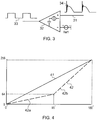
- the straight line 41 shows a transfer function between clock counts (which provides a dimmer level control signal) and the on-time of the pulse modulated signal using a clock or counter with a constant frequency.
- the clock is either an accurate clock which achieves 256 counts over a 180° phase, or may be an inaccurate clock which has been suitably calibrated or tuned as will be further discussed below.
- the response 41 is not ideal.
- a piece-wise linear response as shown at 42 is preferred.
- the concept of a variable frequency clock may be applied: 42 has two sections: a first section 42a with a first gradient, corresponding to the first half of the phase from 0° to 90°; and a second section 42b corresponding to the second half of a phase, from 90° to 180°.
- the gradient of the second section 42b is three times that of the first section 42a, such that the clock count at 90° is 64 in order to achieve a clock count of 256 at 180°
- the half-cycle lasts 10ms, so the 90° phase corresponds to 5ms.
- the clock has to achieve a count of 64 in the first 5 ms, and a further 192 in the final 5 ms.
- the clock must be set to run faster in the second section than the first section - by a factor of three in the example shown. Example configurations of such a clock will be discussed further hereinbelow
- the transfer function shown in figure 5 is another approximation to the ideal logarithmic response.
- Figure 5 shows a transfer function 52, with an initial null-transfer part or level shifting. Again, the curve has two sections: a first section 52a, and a second section 52b.
- the clock runs at a constant rate. The clock starts counting at the start of the period, as shown by curve 51. When the clock reaches a predetermined count, shown as 128 in the exemplary figure and corresponding to a phase of say 60°, the clock is reset, and the count restarts from zero, as shown at curve 52b.
- a flag is used which is unset at the start of the period, and then set when the clock is reset.
- the flag may take the form of a latch.
- counting starts at the rising edge of the pulse modulated signal and stops at the falling edge. If the flag is unset, corresponding to an unlatched output, the output is set to 0; correspondingly, a "set" flag indicates that the response is part of the second part of the curve, and the output is set to the value of the count at the falling edge.
- FIG. 6 shows a further non-linear, piecewise linear, transfer function.
- This transfer function 62 provides a closer approximation to an idealised logarithmic output 61 than either of those described above with reference to figures 4 and 5 . It has three sections, 62a, 62b and 62c, and is a combination of those shown in figure 4 and figure 5 : thus, initially, to produce section 62a of the transfer function, the clock runs at a first speed up to a count of 64, at which moment the flag is set and the counter is reset to zero. The counter then recounts up to a count of 64 - producing the second section 62b of the transfer function. Once the counter reaches 64, the clock speed is increased (in this case by a factor of three) until the end of the period, producing the third section 62c which has a steeper gradient.
- the counting may be started at either a rising or falling edge, since only the complete period is of interest).
- the count has not reached the expected maximum of 256 but only a lower count (shown as 64d in the figure), from which it can be concluded that the clock is running too slow.
- the clock speed is then increased by a small step as will be discussed in more detail below, and the value 65d of the count 65 at the end of the next subsequent period is checked. This is repeated period-by-period until the count at the end of a period has reached the required number (256 in this non-limiting 8-bit example). It is of course necessary to ensure that the clock is running too slow at the start of this calibration phase, which can be readily achieved by choosing to appropriate clock speed.
- FIG. 7 is a schematic block circuit diagram of a circuit arrangement for tuning a clock signal, according to embodiments of the invention is described.
- Figure 7 shows a clock, 70, which comprises a comparator which compares the voltage across the internal capacitor C_internal with a reference voltage VrefC. The capacitor is charged by a current I, until its voltage exceeds VrefC.
- the comparator 71 which may include some hysteresis as shown, then provides a clock pulse though reset pulse generator 72 which also closes switch 73 to discharge the capacitor C_internal.
- the clock speed is thus proportional to the charging current I.
- charging current I is produced by a combination of a first current generator providing current I1, and a series of binary-scaled current generators providing I_diff/16, 1_diff/8, etc., which are separately switchable by means of switches CL0, CL1 etc.
- the total current driving the clock can be varied by small steps of I_diff/16, from I1 up to I1 + 15.I_diff/16.
- the clock output is connected to a series of flip-flops FF0, FF1.. FF7, arranged as an 8-bit register and thus able to store any value from 0 to 255.
- the outputs from the 8-bit register are combined by AND logic 75 the output from the logic 75 is inverted by inverter 76.
- the output from the invertor (255_NOTseen) is combined with AND logic 77, and routed to a linked series of flip-flops 78 which forms a 4-bit register. Sequentially pulse to the 4-bit register result in closing the switches CL0, C1 etc. sequentially, until the counter achieves 255 in a mains half-cycle.
- a different number may be used instead of the number 255 described above.
- 512 could be used.
- the register which can also be considered a counter
- 254 - which is 1 less thatn the maximum obtainable from an 8-bit counter - may by used, or 250 or some other convenient number.
- the case of 254 is particularly convenient for another calibration method, which may be used as an alternative to or in combination with that described above. In this calibration method, the base rate is initially set high, and it is checked whether the counter has reached the desired calibration value too early.
- the counter in various ways, for example - in the case that the counter can exceed the required level - it may be checked whether at the end of the period the counter exceeds the required level such as 254 or 250 mentioned above, or it can be arranged that a flag is set once the required level is achieved, and it is checked whether this flag is set prior to the end of the period, or more specifically, prior by at least a fixed interval before the end of the period.
- the calibration phase is now complete and duty cycle counting can be activated.
- Figure 8 is a schematic block circuit diagram of a circuit having an overall non-linear, but piece-wise linear with level shifting, transfer function.
- the circuit includes a clock tuning circuit 80 corresponding to that shown in figure 7 along with and 8-bit register FF0, FF1.. FF7 for counting.
- An alternative current source including a parallel group 86 of three transistors is shown. Each transistor of 86 is a current mirror which mirrors the current through MOS 84.
- MOS 84 is arranged in parallel to a pair of similar transistors 85, which may be switched by means of switch 86, and all three are in series with current source 85 sourcing current I.
- the switch 86 is closed, so the current from current source 85 is shared equally between MOS 84 and the 2 other transistors.
- the current through MOS 84 is then 1/3.I, as a result of which each transistor in group 86 supplies 1/3.I to the clock tuning circuit - hence the total supplied to clock tuning circuit 80 is I.
- the switch 87 is opened, so the complete current I flows through MOS 84. This is mirrored in each transistor of 84, resulting in a current of 3xI being supplied to the clock tuning circuit 80.
- Additional logic checks the output of FF6 (which indicates whether a count of 64 has been reached and, by means of flip-flop 81, if 64 has been reached for the first time (in the period), in which case it generates at 82 a short pulse to reset the counter.
- FF6 which indicates whether a count of 64 has been reached and, by means of flip-flop 81, if 64 has been reached for the first time (in the period), in which case it generates at 82 a short pulse to reset the counter.
- piece-wise linear when applied to a transfer function, refers to the transfer function as a whole, and refers to transfer functions which have linear sections, but are, overall, non-linear. That is to say, they are only linear to the extent that pieces of the function are linear, and not the whole function.
- a circuit for a dimmer system in which a phase-cut dimmer output signal is converted to a dimming control level signal.
- the phase-cut dimmer output signal is used to dimming control level signal.
- the phase-cut dimmer output signal is used to generated a pulse modulated signal indicative of the duty cycle of the phase cut dimmer output signal, and the pulse modulated signal is directly converted to a piece-wise linear dimming control level signal.
Claims (11)
- Circuit pour système de gradation, le circuit comprenant :une entrée (31) destinée à recevoir un signal de sortie (34) de gradateur à coupure de phase, le signal de sortie de gradateur à coupure de phase présentant une période et des parties coupée et non coupée complémentaires ;une sortie destinée à émettre un signal de niveau de commande de gradation ;un comparateur (32), connecté à l'entrée et agencé pour produire un signal modulé par impulsions (33) à partir du signal de sortie de gradateur à coupure de phase, le signal modulé par impulsions présentant une durée à l'état passant qui varie en fonction de la durée de la partie non coupée ; etun convertisseur configuré pour déterminer le signal de commande de niveau de gradation directement à partir du signal modulé par impulsions afin de déterminer le signal de commande de niveau de gradation et au moyen d'une horloge (70) qui incrémente ou décrémente un compteur (FF0...FF7) à chaque cycle d'horloge pendant la durée à l'état passant, et afin de déterminer le signal de commande de niveau de gradation à partir du compteur,caractérisé en ce queladite horloge (70) présente une fréquence variable de telle sorte que le signal de commande de niveau de gradation présente une relation non linéaire mais linéaire par morceaux (42) avec la partie non coupée.
- Circuit selon la revendication 1, dans lequel
l'horloge est agencée pour fonctionner à une fréquence initiale pendant une partie initiale de la période, ladite fréquence initiale étant en relation fixe avec une fréquence de base, et pour, quand le compteur atteint un nombre prédéfini, terminer la partie initiale, placer un drapeau, et remettre le compteur à zéro ;
le circuit étant en outre configuré pour régler le signal de niveau de commande de gradation à un niveau complètement réduit si le drapeau n'est pas placé. - Circuit selon la revendication 1, dans lequel
l'horloge est agencée pour fonctionner à une première fréquence sur une première partie de la période et à une seconde fréquence sur une seconde partie de la période,
la première fréquence étant en relation fixe avec une fréquence de base et la seconde fréquence étant en relation fixe avec la première fréquence et supérieure à celle-ci et la seconde partie de la période se trouvant plus tard dans la période que la première partie de la période. - Circuit selon la revendication 2, dans lequel
l'horloge est agencée pour fonctionner à une fréquence initiale pendant une partie initiale de la période, qui précède aussi bien la première partie que la seconde partie dans la période, et pour, quand le compteur atteint un nombre prédéfini, terminer la partie initiale, placer un drapeau, et remettre le compteur à zéro ;
le circuit étant en outre configuré pour régler le signal de niveau de commande de gradation à un niveau complètement réduit si le drapeau n'est pas placé. - Circuit selon l'une quelconque des revendications 2 à 4, configuré en outre pour effectuer une phase d'étalonnage dans laquelle respectivement la fréquence de base est ajustée vers le haut période par période en réponse au fait que le compteur n'atteint pas un second nombre prédéfini pendant une période et/ou la fréquence de base est ajustée vers le bas période par période en réponse au fait que le compteur dépasse le second nombre prédéfini pendant la période.
- Circuit selon l'une quelconque des revendications 2 à 4, configuré en outre pour effectuer une phase d'étalonnage dans laquelle la fréquence de base est ajustée vers le bas période par période en réponse au fait que le compteur atteint un second nombre prédéfini avant la fin d'une période.
- Dispositif de commande pour système d'éclairage à intensité variable comprenant un gradateur à coupure de phase et un circuit selon l'une quelconque des revendications précédentes.
- Procédé de détermination d'un niveau de commande de gradation à partir d'un signal de sortie (34) de gradateur à coupure de phase présentant une période et des parties coupée et non coupée complémentaires, le procédé comprenant- la détermination d'un signal modulé par impulsions à partir du signal de sortie (33) de gradateur à coupure de phase, le signal modulé par impulsions présentant une durée à l'état passant qui varie en fonction de la durée de la partie non coupée ; et- la détermination du signal de niveau de commande de gradation directement à partir du signal modulé par impulsions la détermination du signal de niveau commande de gradation directement à partir du signal modulé en impulsions comprenant
l'incrémentation d'un compteur d'une horloge à chaque cycle d'horloge pendant la durée à l'état passant, et
la détermination du signal de commande de niveau de gradation à partir du compteur
caractérisé en ce que
ladite horloge présente une fréquence variable de telle sorte que le niveau de commande de gradation présente une relation non linéaire, linéaire par morceaux (42) avec la partie coupée. - Procédé selon la revendication 8, comprenant en outre le fonctionnement de l'horloge à une fréquence initiale pendant une partie initiale de la période, ladite fréquence initiale étant en relation fixe avec une fréquence de base, et
quand le compteur atteint un nombre prédéfini, la terminaison de la partie initiale, le placement d'un drapeau, et la remise à zéro du compteur ; et
le réglage du signal de niveau de commande de gradation à un niveau complètement réduit si le drapeau n'est pas placé. - Procédé selon la revendication 9, comprenant en outre le fonctionnement de l'horloge à une première fréquence sur une première partie de la période et à une seconde fréquence sur une seconde partie de la période, la première fréquence étant en relation fixe avec une fréquence de base et la seconde fréquence en relation fixe avec la première fréquence et supérieure à celle-ci et la seconde partie de la période se trouvant plus tard dans la période que la première partie de la période.
- Procédé selon la revendication 10, comprenant en outre le fonctionnement de l'horloge à une fréquence initiale pendant une partie initiale de la période, qui précède aussi bien la première partie que la seconde partie dans la période, et quand le compteur atteint un nombre prédéfini, la terminaison de la partie initiale, le placement d'un drapeau, et la remise à zéro du compteur ; et le réglage du signal de niveau de commande de gradation à un niveau complètement réduit si le drapeau n'est pas placé.
Priority Applications (4)
| Application Number | Priority Date | Filing Date | Title |
|---|---|---|---|
| EP10186908.9A EP2440020B1 (fr) | 2010-10-07 | 2010-10-07 | Génération à partir de la sortie d'un gradateur à coupure de phase à réponse rapide à des changements dans la position du gradateur |
| PL10186908T PL2440020T3 (pl) | 2010-10-07 | 2010-10-07 | Generacja z wyjścia ściemniacza z odcięciem fazy z szybką reakcją na zmiany w pozycji ściemniacza |
| CN201110302152.3A CN102448227B (zh) | 2010-10-07 | 2011-09-28 | 用于调光器系统的电路、调光器系统及操作调光器系统的方法 |
| US13/267,819 US9137880B2 (en) | 2010-10-07 | 2011-10-06 | Generation from phase cut dimmer output with fast response to changes in dimmer position |
Applications Claiming Priority (1)
| Application Number | Priority Date | Filing Date | Title |
|---|---|---|---|
| EP10186908.9A EP2440020B1 (fr) | 2010-10-07 | 2010-10-07 | Génération à partir de la sortie d'un gradateur à coupure de phase à réponse rapide à des changements dans la position du gradateur |
Publications (2)
| Publication Number | Publication Date |
|---|---|
| EP2440020A1 EP2440020A1 (fr) | 2012-04-11 |
| EP2440020B1 true EP2440020B1 (fr) | 2016-12-28 |
Family
ID=43896751
Family Applications (1)
| Application Number | Title | Priority Date | Filing Date |
|---|---|---|---|
| EP10186908.9A Active EP2440020B1 (fr) | 2010-10-07 | 2010-10-07 | Génération à partir de la sortie d'un gradateur à coupure de phase à réponse rapide à des changements dans la position du gradateur |
Country Status (4)
| Country | Link |
|---|---|
| US (1) | US9137880B2 (fr) |
| EP (1) | EP2440020B1 (fr) |
| CN (1) | CN102448227B (fr) |
| PL (1) | PL2440020T3 (fr) |
Families Citing this family (9)
| Publication number | Priority date | Publication date | Assignee | Title |
|---|---|---|---|---|
| JP6143759B2 (ja) * | 2011-10-14 | 2017-06-07 | フィリップス ライティング ホールディング ビー ヴィ | 固体照明装置の調光を制御するシステム及び方法 |
| US9692954B2 (en) * | 2013-03-28 | 2017-06-27 | General Electric Company | Methods and devices for adjusting brightness of a light source |
| US9379606B2 (en) * | 2013-05-30 | 2016-06-28 | Apple Inc. | Discrete narrow-band switching frequency avoidance of a switch mode power converter |
| EP2953426B1 (fr) | 2014-06-06 | 2017-08-30 | Silergy Corp. | Alimentation électrique de mode commuté |
| CN107666741B (zh) * | 2017-10-11 | 2020-02-21 | 宁波赛耐比光电科技股份有限公司 | 一种pwm调光电路 |
| CN110324927B (zh) * | 2018-03-28 | 2021-09-24 | 圣邦微电子(北京)股份有限公司 | 一种驱动led的pwm信号的产生方法 |
| EP3847872B1 (fr) * | 2018-09-05 | 2023-11-08 | The Gillette Company LLC | Modulation d'un niveau d'éclairage d'un élément lumineux d'interface utilisateur |
| CN109379804B (zh) * | 2018-10-15 | 2023-12-22 | 广东宝莱特医用科技股份有限公司 | 一种led灯调光系统及调光方法 |
| CN111163558B (zh) * | 2018-11-08 | 2022-02-25 | 松下知识产权经营株式会社 | 调光曲线校正方法及单元、led照明装置及存储介质 |
Family Cites Families (6)
| Publication number | Priority date | Publication date | Assignee | Title |
|---|---|---|---|---|
| US7667408B2 (en) * | 2007-03-12 | 2010-02-23 | Cirrus Logic, Inc. | Lighting system with lighting dimmer output mapping |
| US8115419B2 (en) | 2008-01-23 | 2012-02-14 | Cree, Inc. | Lighting control device for controlling dimming, lighting device including a control device, and method of controlling lighting |
| US8102167B2 (en) * | 2008-03-25 | 2012-01-24 | Microsemi Corporation | Phase-cut dimming circuit |
| US8829812B2 (en) * | 2008-04-04 | 2014-09-09 | Koninklijke Philips N.V. | Dimmable lighting system |
| CN101646289A (zh) * | 2009-06-29 | 2010-02-10 | 潘忠浩 | 调光调速控制电路及控制方法 |
| US8736191B2 (en) * | 2009-10-14 | 2014-05-27 | National Semiconductor Corporation | Dimmer decoder with adjustable filter for use with LED drivers |
-
2010
- 2010-10-07 PL PL10186908T patent/PL2440020T3/pl unknown
- 2010-10-07 EP EP10186908.9A patent/EP2440020B1/fr active Active
-
2011
- 2011-09-28 CN CN201110302152.3A patent/CN102448227B/zh active Active
- 2011-10-06 US US13/267,819 patent/US9137880B2/en active Active
Non-Patent Citations (1)
| Title |
|---|
| None * |
Also Published As
| Publication number | Publication date |
|---|---|
| CN102448227B (zh) | 2014-07-23 |
| EP2440020A1 (fr) | 2012-04-11 |
| US9137880B2 (en) | 2015-09-15 |
| PL2440020T3 (pl) | 2017-05-31 |
| CN102448227A (zh) | 2012-05-09 |
| US20120086354A1 (en) | 2012-04-12 |
Similar Documents
| Publication | Publication Date | Title |
|---|---|---|
| EP2440020B1 (fr) | Génération à partir de la sortie d'un gradateur à coupure de phase à réponse rapide à des changements dans la position du gradateur | |
| US8643301B2 (en) | LED driver circuit and LED lighting device using the same | |
| EP2885575B1 (fr) | Procédé et appareil pour commander une intensité lumineuse en fonction de fluctuations d'une tension | |
| EP3367761B1 (fr) | Dispositif de contrôle de charge pour charges à haute efficacité | |
| EP3518623A1 (fr) | Module de circuit, circuit de commande de diode électroluminescente à gradation et procédé de commande | |
| CN105992440B (zh) | Led驱动器的控制电路及方法 | |
| EP2311298B1 (fr) | Procédé et agencement de circuit de e régulation d'un courant del traversant un circuit del, et composition de circuit et système d'éclairage connexe | |
| US8653751B2 (en) | LED drive circuit and LED illumination component using the same | |
| US20100219764A1 (en) | Led dimming apparatus | |
| EP2130406A2 (fr) | Système d'éclairage avec mise en correspondance de sortie de variateur d'éclairage | |
| EP1884143A2 (fr) | Procede et systeme de gradation de tension universelle de secteur | |
| US5994883A (en) | Alternating current power control device | |
| US20150084534A1 (en) | Lighting apparatus and illumination system using the same | |
| US20200037410A1 (en) | Apparatus and methods for controlling led light flux | |
| EP3641504A1 (fr) | Circuit intégré, circuit de commande de diode électroluminescente à intensité variable et procédé de commande | |
| US9839086B2 (en) | Technique for adjusting the brightness of LED lamps | |
| US9246378B2 (en) | Method and apparatus for extending the power output range of a power converter used for a lighting system | |
| CN111542148B (zh) | Led驱动模块 | |
| TW201345312A (zh) | 用於一多相系統中發光二極體之恆定照射及色彩控制之系統及方法 | |
| CN102893527A (zh) | 用于fpga的时钟的电路 | |
| EP2806712A1 (fr) | Circuit d'application et son procédé de commande | |
| US8664894B2 (en) | Method and device for driving a fluorescent lamp | |
| CN111194119A (zh) | 一种可开关调光控制的led驱动电路及方法 | |
| JP7442189B2 (ja) | 調光装置および調光方法 | |
| JP2011044353A (ja) | 調光器 |
Legal Events
| Date | Code | Title | Description |
|---|---|---|---|
| AK | Designated contracting states |
Kind code of ref document: A1 Designated state(s): AL AT BE BG CH CY CZ DE DK EE ES FI FR GB GR HR HU IE IS IT LI LT LU LV MC MK MT NL NO PL PT RO RS SE SI SK SM TR |
|
| AX | Request for extension of the european patent |
Extension state: BA ME |
|
| PUAI | Public reference made under article 153(3) epc to a published international application that has entered the european phase |
Free format text: ORIGINAL CODE: 0009012 |
|
| 17P | Request for examination filed |
Effective date: 20121011 |
|
| 17Q | First examination report despatched |
Effective date: 20130926 |
|
| RAP1 | Party data changed (applicant data changed or rights of an application transferred) |
Owner name: SILERGY CORP. |
|
| GRAP | Despatch of communication of intention to grant a patent |
Free format text: ORIGINAL CODE: EPIDOSNIGR1 |
|
| INTG | Intention to grant announced |
Effective date: 20160825 |
|
| GRAS | Grant fee paid |
Free format text: ORIGINAL CODE: EPIDOSNIGR3 |
|
| GRAA | (expected) grant |
Free format text: ORIGINAL CODE: 0009210 |
|
| AK | Designated contracting states |
Kind code of ref document: B1 Designated state(s): AL AT BE BG CH CY CZ DE DK EE ES FI FR GB GR HR HU IE IS IT LI LT LU LV MC MK MT NL NO PL PT RO RS SE SI SK SM TR |
|
| REG | Reference to a national code |
Ref country code: GB Ref legal event code: FG4D |
|
| REG | Reference to a national code |
Ref country code: CH Ref legal event code: EP |
|
| REG | Reference to a national code |
Ref country code: CH Ref legal event code: NV Representative=s name: ISLER AND PEDRAZZINI AG, CH |
|
| REG | Reference to a national code |
Ref country code: AT Ref legal event code: REF Ref document number: 858267 Country of ref document: AT Kind code of ref document: T Effective date: 20170115 |
|
| REG | Reference to a national code |
Ref country code: IE Ref legal event code: FG4D |
|
| REG | Reference to a national code |
Ref country code: DE Ref legal event code: R096 Ref document number: 602010039107 Country of ref document: DE |
|
| REG | Reference to a national code |
Ref country code: NL Ref legal event code: FP |
|
| PG25 | Lapsed in a contracting state [announced via postgrant information from national office to epo] |
Ref country code: LV Free format text: LAPSE BECAUSE OF FAILURE TO SUBMIT A TRANSLATION OF THE DESCRIPTION OR TO PAY THE FEE WITHIN THE PRESCRIBED TIME-LIMIT Effective date: 20161228 |
|
| REG | Reference to a national code |
Ref country code: LT Ref legal event code: MG4D |
|
| PG25 | Lapsed in a contracting state [announced via postgrant information from national office to epo] |
Ref country code: GR Free format text: LAPSE BECAUSE OF FAILURE TO SUBMIT A TRANSLATION OF THE DESCRIPTION OR TO PAY THE FEE WITHIN THE PRESCRIBED TIME-LIMIT Effective date: 20170329 Ref country code: NO Free format text: LAPSE BECAUSE OF FAILURE TO SUBMIT A TRANSLATION OF THE DESCRIPTION OR TO PAY THE FEE WITHIN THE PRESCRIBED TIME-LIMIT Effective date: 20170328 Ref country code: LT Free format text: LAPSE BECAUSE OF FAILURE TO SUBMIT A TRANSLATION OF THE DESCRIPTION OR TO PAY THE FEE WITHIN THE PRESCRIBED TIME-LIMIT Effective date: 20161228 Ref country code: SE Free format text: LAPSE BECAUSE OF FAILURE TO SUBMIT A TRANSLATION OF THE DESCRIPTION OR TO PAY THE FEE WITHIN THE PRESCRIBED TIME-LIMIT Effective date: 20161228 |
|
| REG | Reference to a national code |
Ref country code: AT Ref legal event code: MK05 Ref document number: 858267 Country of ref document: AT Kind code of ref document: T Effective date: 20161228 |
|
| PG25 | Lapsed in a contracting state [announced via postgrant information from national office to epo] |
Ref country code: HR Free format text: LAPSE BECAUSE OF FAILURE TO SUBMIT A TRANSLATION OF THE DESCRIPTION OR TO PAY THE FEE WITHIN THE PRESCRIBED TIME-LIMIT Effective date: 20161228 Ref country code: RS Free format text: LAPSE BECAUSE OF FAILURE TO SUBMIT A TRANSLATION OF THE DESCRIPTION OR TO PAY THE FEE WITHIN THE PRESCRIBED TIME-LIMIT Effective date: 20161228 |
|
| PG25 | Lapsed in a contracting state [announced via postgrant information from national office to epo] |
Ref country code: RO Free format text: LAPSE BECAUSE OF FAILURE TO SUBMIT A TRANSLATION OF THE DESCRIPTION OR TO PAY THE FEE WITHIN THE PRESCRIBED TIME-LIMIT Effective date: 20161228 Ref country code: SK Free format text: LAPSE BECAUSE OF FAILURE TO SUBMIT A TRANSLATION OF THE DESCRIPTION OR TO PAY THE FEE WITHIN THE PRESCRIBED TIME-LIMIT Effective date: 20161228 Ref country code: IS Free format text: LAPSE BECAUSE OF FAILURE TO SUBMIT A TRANSLATION OF THE DESCRIPTION OR TO PAY THE FEE WITHIN THE PRESCRIBED TIME-LIMIT Effective date: 20170428 Ref country code: EE Free format text: LAPSE BECAUSE OF FAILURE TO SUBMIT A TRANSLATION OF THE DESCRIPTION OR TO PAY THE FEE WITHIN THE PRESCRIBED TIME-LIMIT Effective date: 20161228 Ref country code: CZ Free format text: LAPSE BECAUSE OF FAILURE TO SUBMIT A TRANSLATION OF THE DESCRIPTION OR TO PAY THE FEE WITHIN THE PRESCRIBED TIME-LIMIT Effective date: 20161228 |
|
| PG25 | Lapsed in a contracting state [announced via postgrant information from national office to epo] |
Ref country code: AT Free format text: LAPSE BECAUSE OF FAILURE TO SUBMIT A TRANSLATION OF THE DESCRIPTION OR TO PAY THE FEE WITHIN THE PRESCRIBED TIME-LIMIT Effective date: 20161228 Ref country code: ES Free format text: LAPSE BECAUSE OF FAILURE TO SUBMIT A TRANSLATION OF THE DESCRIPTION OR TO PAY THE FEE WITHIN THE PRESCRIBED TIME-LIMIT Effective date: 20161228 Ref country code: SM Free format text: LAPSE BECAUSE OF FAILURE TO SUBMIT A TRANSLATION OF THE DESCRIPTION OR TO PAY THE FEE WITHIN THE PRESCRIBED TIME-LIMIT Effective date: 20161228 Ref country code: BE Free format text: LAPSE BECAUSE OF FAILURE TO SUBMIT A TRANSLATION OF THE DESCRIPTION OR TO PAY THE FEE WITHIN THE PRESCRIBED TIME-LIMIT Effective date: 20161228 Ref country code: BG Free format text: LAPSE BECAUSE OF FAILURE TO SUBMIT A TRANSLATION OF THE DESCRIPTION OR TO PAY THE FEE WITHIN THE PRESCRIBED TIME-LIMIT Effective date: 20170328 Ref country code: PT Free format text: LAPSE BECAUSE OF FAILURE TO SUBMIT A TRANSLATION OF THE DESCRIPTION OR TO PAY THE FEE WITHIN THE PRESCRIBED TIME-LIMIT Effective date: 20170428 |
|
| REG | Reference to a national code |
Ref country code: DE Ref legal event code: R097 Ref document number: 602010039107 Country of ref document: DE |
|
| REG | Reference to a national code |
Ref country code: FR Ref legal event code: PLFP Year of fee payment: 8 |
|
| PLBE | No opposition filed within time limit |
Free format text: ORIGINAL CODE: 0009261 |
|
| STAA | Information on the status of an ep patent application or granted ep patent |
Free format text: STATUS: NO OPPOSITION FILED WITHIN TIME LIMIT |
|
| PG25 | Lapsed in a contracting state [announced via postgrant information from national office to epo] |
Ref country code: DK Free format text: LAPSE BECAUSE OF FAILURE TO SUBMIT A TRANSLATION OF THE DESCRIPTION OR TO PAY THE FEE WITHIN THE PRESCRIBED TIME-LIMIT Effective date: 20161228 |
|
| 26N | No opposition filed |
Effective date: 20170929 |
|
| PG25 | Lapsed in a contracting state [announced via postgrant information from national office to epo] |
Ref country code: SI Free format text: LAPSE BECAUSE OF FAILURE TO SUBMIT A TRANSLATION OF THE DESCRIPTION OR TO PAY THE FEE WITHIN THE PRESCRIBED TIME-LIMIT Effective date: 20161228 |
|
| PG25 | Lapsed in a contracting state [announced via postgrant information from national office to epo] |
Ref country code: MC Free format text: LAPSE BECAUSE OF FAILURE TO SUBMIT A TRANSLATION OF THE DESCRIPTION OR TO PAY THE FEE WITHIN THE PRESCRIBED TIME-LIMIT Effective date: 20161228 |
|
| REG | Reference to a national code |
Ref country code: CH Ref legal event code: PL |
|
| REG | Reference to a national code |
Ref country code: NL Ref legal event code: MM Effective date: 20171101 |
|
| REG | Reference to a national code |
Ref country code: IE Ref legal event code: MM4A |
|
| PG25 | Lapsed in a contracting state [announced via postgrant information from national office to epo] |
Ref country code: FI Free format text: LAPSE BECAUSE OF NON-PAYMENT OF DUE FEES Effective date: 20171007 Ref country code: LU Free format text: LAPSE BECAUSE OF NON-PAYMENT OF DUE FEES Effective date: 20171007 Ref country code: CH Free format text: LAPSE BECAUSE OF NON-PAYMENT OF DUE FEES Effective date: 20171031 Ref country code: LI Free format text: LAPSE BECAUSE OF NON-PAYMENT OF DUE FEES Effective date: 20171031 Ref country code: NL Free format text: LAPSE BECAUSE OF NON-PAYMENT OF DUE FEES Effective date: 20171101 |
|
| PG25 | Lapsed in a contracting state [announced via postgrant information from national office to epo] |
Ref country code: MT Free format text: LAPSE BECAUSE OF NON-PAYMENT OF DUE FEES Effective date: 20171007 |
|
| PG25 | Lapsed in a contracting state [announced via postgrant information from national office to epo] |
Ref country code: IT Free format text: LAPSE BECAUSE OF NON-PAYMENT OF DUE FEES Effective date: 20171007 Ref country code: IE Free format text: LAPSE BECAUSE OF NON-PAYMENT OF DUE FEES Effective date: 20171007 |
|
| REG | Reference to a national code |
Ref country code: FR Ref legal event code: PLFP Year of fee payment: 9 |
|
| PG25 | Lapsed in a contracting state [announced via postgrant information from national office to epo] |
Ref country code: PL Free format text: LAPSE BECAUSE OF NON-PAYMENT OF DUE FEES Effective date: 20171007 |
|
| PG25 | Lapsed in a contracting state [announced via postgrant information from national office to epo] |
Ref country code: HU Free format text: LAPSE BECAUSE OF FAILURE TO SUBMIT A TRANSLATION OF THE DESCRIPTION OR TO PAY THE FEE WITHIN THE PRESCRIBED TIME-LIMIT; INVALID AB INITIO Effective date: 20101007 |
|
| PG25 | Lapsed in a contracting state [announced via postgrant information from national office to epo] |
Ref country code: CY Free format text: LAPSE BECAUSE OF NON-PAYMENT OF DUE FEES Effective date: 20161228 |
|
| PG25 | Lapsed in a contracting state [announced via postgrant information from national office to epo] |
Ref country code: MK Free format text: LAPSE BECAUSE OF FAILURE TO SUBMIT A TRANSLATION OF THE DESCRIPTION OR TO PAY THE FEE WITHIN THE PRESCRIBED TIME-LIMIT Effective date: 20161228 |
|
| PG25 | Lapsed in a contracting state [announced via postgrant information from national office to epo] |
Ref country code: AL Free format text: LAPSE BECAUSE OF FAILURE TO SUBMIT A TRANSLATION OF THE DESCRIPTION OR TO PAY THE FEE WITHIN THE PRESCRIBED TIME-LIMIT Effective date: 20161228 |
|
| REG | Reference to a national code |
Ref country code: GB Ref legal event code: 732E Free format text: REGISTERED BETWEEN 20210527 AND 20210602 |
|
| REG | Reference to a national code |
Ref country code: DE Ref legal event code: R082 Ref document number: 602010039107 Country of ref document: DE Representative=s name: LORENZ SEIDLER GOSSEL RECHTSANWAELTE PATENTANW, DE Ref country code: DE Ref legal event code: R081 Ref document number: 602010039107 Country of ref document: DE Owner name: SILERGY SEMICONDUCTOR (HONG KONG) LTD., HK Free format text: FORMER OWNER: SILERGY CORP., GRAND CAYMAN, KY |
|
| PGFP | Annual fee paid to national office [announced via postgrant information from national office to epo] |
Ref country code: GB Payment date: 20231019 Year of fee payment: 14 |
|
| PGFP | Annual fee paid to national office [announced via postgrant information from national office to epo] |
Ref country code: FR Payment date: 20231023 Year of fee payment: 14 Ref country code: DE Payment date: 20231011 Year of fee payment: 14 |