EP2439930A2 - Improvements in or relating to dynamic range enhancement of imaging sensors. - Google Patents
Improvements in or relating to dynamic range enhancement of imaging sensors. Download PDFInfo
- Publication number
- EP2439930A2 EP2439930A2 EP11184117A EP11184117A EP2439930A2 EP 2439930 A2 EP2439930 A2 EP 2439930A2 EP 11184117 A EP11184117 A EP 11184117A EP 11184117 A EP11184117 A EP 11184117A EP 2439930 A2 EP2439930 A2 EP 2439930A2
- Authority
- EP
- European Patent Office
- Prior art keywords
- pixel
- integration time
- value
- max
- reference values
- Prior art date
- Legal status (The legal status is an assumption and is not a legal conclusion. Google has not performed a legal analysis and makes no representation as to the accuracy of the status listed.)
- Granted
Links
Images
Classifications
-
- H—ELECTRICITY
- H04—ELECTRIC COMMUNICATION TECHNIQUE
- H04N—PICTORIAL COMMUNICATION, e.g. TELEVISION
- H04N23/00—Cameras or camera modules comprising electronic image sensors; Control thereof
- H04N23/70—Circuitry for compensating brightness variation in the scene
- H04N23/73—Circuitry for compensating brightness variation in the scene by influencing the exposure time
-
- H—ELECTRICITY
- H04—ELECTRIC COMMUNICATION TECHNIQUE
- H04N—PICTORIAL COMMUNICATION, e.g. TELEVISION
- H04N23/00—Cameras or camera modules comprising electronic image sensors; Control thereof
- H04N23/70—Circuitry for compensating brightness variation in the scene
- H04N23/741—Circuitry for compensating brightness variation in the scene by increasing the dynamic range of the image compared to the dynamic range of the electronic image sensors
-
- H—ELECTRICITY
- H04—ELECTRIC COMMUNICATION TECHNIQUE
- H04N—PICTORIAL COMMUNICATION, e.g. TELEVISION
- H04N25/00—Circuitry of solid-state image sensors [SSIS]; Control thereof
- H04N25/50—Control of the SSIS exposure
- H04N25/57—Control of the dynamic range
-
- H—ELECTRICITY
- H04—ELECTRIC COMMUNICATION TECHNIQUE
- H04N—PICTORIAL COMMUNICATION, e.g. TELEVISION
- H04N25/00—Circuitry of solid-state image sensors [SSIS]; Control thereof
- H04N25/50—Control of the SSIS exposure
- H04N25/57—Control of the dynamic range
- H04N25/58—Control of the dynamic range involving two or more exposures
- H04N25/581—Control of the dynamic range involving two or more exposures acquired simultaneously
- H04N25/583—Control of the dynamic range involving two or more exposures acquired simultaneously with different integration times
-
- H—ELECTRICITY
- H04—ELECTRIC COMMUNICATION TECHNIQUE
- H04N—PICTORIAL COMMUNICATION, e.g. TELEVISION
- H04N25/00—Circuitry of solid-state image sensors [SSIS]; Control thereof
- H04N25/50—Control of the SSIS exposure
- H04N25/57—Control of the dynamic range
- H04N25/59—Control of the dynamic range by controlling the amount of charge storable in the pixel, e.g. modification of the charge conversion ratio of the floating node capacitance
Definitions
- the present invention relates to improvements in dynamic range enhancement and is more particularly concerned with dynamic range enhancement through prediction of pixel integration time.
- Dynamic range is one of the most important features of imaging sensors as it provides the ability of a detector to capture highlights and shadows in the same frame. It is determined in accordance with the quality of the elements used to make the imaging sensor, that is, the quality of the pixels.
- the dark-to-light contrast in the same frame, is typically limited to between 60 and 70dB. This range is low compared to the dark-to-light contrast that can be obtained with the human eye.
- Logarithmic pixel response can provide a simple pixel architecture through which high DR can be obtained.
- Such a method of increasing DR is described in " Wide-Dynamic-Range CMOS Image Sensors ⁇ Comparative Performance Analysis" by A Spivak, A Belenky, A Fish, and O Yadid-Pecht, Electron Devices, IEEE Transactions, pages 2446 to 2461, 2009 .
- the lateral overflow method collects the charges generated by a high luminance in an extra capacitor as described by S Sugawa, N Akahane, S Adachi, K Mori, T lshiuchi and K Mizobuchi in "A 100dB Dynamic Range CMOS Image Sensor using a Lateral Overflow Integration Capacitor", Solid-State Circuits Conference, Digest of Technical Papers, ISSCC 2005 IEEE International, Volume 1, pages 352 to 603, 2005 .
- This technique introduces a signal-to-noise ratio (SNR) dip at mid-light which degrades the performance of the sensor once the required DR becomes high, that is, more than 100dB. This is due to the switching between the high conversion gain of the floating diffusion node and the low conversion gain of the lateral overflow capacitor.
- SNR signal-to-noise ratio
- MCT multiple captures techniques
- n the number of captures needed for a certain DR
- T imt (i) represents the integration time of a capture " i "
- T AD represents the analogue-to-digital (AD) conversion time
- T ro represents the pixel readout time.
- the multiple AD conversions needed per pixel typically, one for each capture, and the image processing required to reconstruct the final image increase the overall power consumption of the imaging sensor.
- SNR dip 20 ⁇ log 10 T max T min where T max represents the long capture time and T min represents the short capture time.
- the consequent SNR dip would decrese the image quality at mid-light levels. This means that the DR enhancement or extension obtained depends on the maximum SNR dip in accordance with the specific application.
- an imaging sensor comprises a plurality of pixels that provide a DR of 60dB and it is desired to increase the DR to 120dB, ten extra captures are needed to provide a DR enhancement or extension of 60dB, where each capture provides an extra 6dB.
- a method of increasing the dynamic range of at least one pixel in a pixel array comprising the steps of:
- the dynamic range of each pixel in the pixel array can be extended without the necessity of having to take many captures.
- only two captures are required, that is, the capture at the predetermined integration time and the capture at the optimum integration time. This leads to a reduction in both processing time and processing power.
- frame rate is not substantially compromised as only two of captures need to be taken.
- step b) further comprises the step of predicting the optimum integration time for each pixel in the pixel array in accordance with the comparison between the determined electrical value and the set of reference values.
- step b) comprises setting the set of reference values as fractional multiples of the saturation electrical value. This means that, by knowing the nominal saturation electrical value of each pixel, it is possible to set a number of reference values which assist in the determination of the optimum integration time.
- step b) may comprise setting the set of reference values as fractional multiples of the pixel output electrical swing value, V swing .
- the optimum integration time is T int (i) when the electrical value (V c1 ) is between V t (i) and V t (i+1), and T max when the electrical value ( V c1 ) is lower than V t (n) where n is the number of sub-integration intervals.
- the method may further comprise the steps of c) estimating an offset for each pixel when the electrical value of each pixel causes the integration time thereof to be increased; and d) lowering the integration time of each pixel in accordance with the estimated offset.
- the method may further comprise the step of adjusting for variability in light values by reducing the values of the set of reference values.
- the method preferably further comprises the step e) of reading out an electrical value from each pixel in accordance with the actual integration time.
- Step e) may comprise destructively reading out the electrical value or non-destructively reading out the electrical value.
- the method further comprises performing steps a) to e) for a group of pixels within the imaging array. In this way, an optimum integration time for the group of pixels can be predicted.
- US-B-6995801 describes an imaging system in which the integration values are compared to upper and lower threshold values to control the imaging system. If the integration value is below the lower threshold value, an acceleration signal is generated. If the integration value is above the upper threshold value, a suppression signal is generated. If the integration value falls between the upper and lower threshold values, a fixed exposure signal is generated. The acceleration, suppression and fixed exposure signals are used to control the integration times of the imaging system.
- US-A-5793422 and EP-A-0583143 relate to electronic shutter control in video cameras. In both cases, the output of a low pass filter is compared to different threshold values to control the iris for the video camera.
- the exposure time of the imaging sensor is controlled in accordance with a comparison between an output signal corresponding to the charges generated by the imaging sensor and a number of reference levels.
- upper and lower reference levels bound a dead zone, the reference levels being controlled in accordance with the exposure time by increasing an absolute difference between the upper and lower reference levels as the exposure time decreases.
- WO-A-2009/073054 describes an imaging device in which the light induced charge for each pixel in a row is compared against a threshold level to determine whether or not to reset the pixels in the row as a result of the comparison.
- the core element of the method of the present invention is the prediction of the optimum integration time for a single pixel or a group of pixels.
- the situation relating to a single pixel and its integration time will be described but it will readily be understood that the situation is also applicable to a group of pixels.
- a first capture is made to predict the best integration time of the pixel or group of pixels.
- a second capture is made according to the optimum integration time predicted by the first capture. The higher the dynamic range required, the shorter the integration time needed for the first capture and the higher the advantages over the normal multiple captures technique.
- wide dynamic range is defined as the ratio of the brightest point of an image to the darkest point of the same image.
- luminance is the total luminous flux incident on a surface, per unit area. It is a measure of the intensity of the incident light, wavelength-weighted by the luminosity function to correlate with human brightness perception.
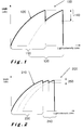
- a typical SNR characteristic 100 of a sensor employing a lateral overflow technique is shown.
- the characteristic 100 comprises a graph of SNR against light intensity.
- a normal sensor characteristic 110 is shown together with a characteristic 120 due to an overflow capacitor.
- the two characteristics 110, 120 overlap to form a final sensor characteristic 130, as shown by the solid line, with a certain SNR dip 140 which depends on the distance between the two characteristics 110, 120. The greater the distance between the two characteristics 110, 120, the greater the DR obtained and the SNR dip.
- T The integration time, T, of a pixel is directly proportional to the charges it accumulates: T ⁇ Q I where Q is the amount of charge accumulated and I is the illuminance.
- a short integration time is required to avoid pixel saturation, that is, the point at which the pixel has reached the maximum charge it can collect.
- a short integration time also tends to limit the charge accumulated if the light level is low. This results in low SNR or even an unrecognisable light signal.
- a MCT can be implemented. Each integration time can be chosen to be the double of the previous one so that if the shortest integration time is T 1 then T 2 will be 2T 1 , T3 will be 2T 2 , etc.
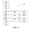
- Figure 2 illustrates the typical characteristic 200 of a sensor integrating three times. (The scale of Figure 2 is different to that of Figure 1 .)
- the final SNR characteristic 210 is obtained by the overlapping of each capture SNR characteristic, that is, the normal DR 230 and two overlapping characteristics to provide the DR extension 240.
- a SNR dip 250 is still obtained. If each subsequent integration time is double the previous one, the enhanced DR obtained is 6dB per extra capture and the SNR dip is 3dB.
- the electrical output signal of the pixels is assumed to increase as the light intensity increases.
- the electrical value of the pixel is compared with a reference voltage value.
- This reference voltage value is usually half of the full voltage range of the pixel, that is, its saturation voltage.
- the voltage value is used as the pixel electrical value, but it will be appreciated that other representations of the pixel electrical value can be used.
- the voltage of the pixel and the corresponding integration time are digitised.
- Each capture time corresponds to a left shifting of the digitised pixel value.
- the chosen integration time is T 1 , that is, the shortest integration time
- the fine pixel conversion of 8-bit is shifted left to the most significant bit.
- T 1 that is, the shortest integration time
- the fine pixel conversion of 8-bit is shifted left to the most significant bit.
- the extension of dynamic range obtained with MCT corresponds to 6dB for each extra integration time or period. If a basic sensor provides 60dB of DR, 10 extra captures are needed to extend the DR to 120dB.
- the method in accordance with the present invention integrates only twice for each pixel.
- the first integration comprises a short integration time which is used to predict an optimum value for the second integration time.
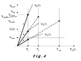
- FIG. 3 illustrates a flow chart 300 showing an implementation of the method of DR enhancement or extension in accordance with the present invention.
- the first step, step 305 is to take the first capture with the shortest integration time, T int (1) , and to store the voltage, V c1 , relating to this first capture, step 310.
- step 315 before each T ⁇ nt (i), V cl , is compared to V t ( i +1 ).
- the voltage read is stored in a sample-and-hold (S&H) circuit, the mantissa bit is sent for storage in a digital memory in order to perform a floating point DR extension, step 330, and a "veto" signal is sent back to the pixel to avoid further integrations within the same frame.
- S&H sample-and-hold
- V c 1 ⁇ V t (2)
- V t (3) a second lower threshold value
- V c 1 V t (3)
- the process is repeated until the i th comparison, step 355.
- the voltage corresponding to the predicted integration time is sent for analogue-to-digital conversion (ADC) in step 335.
- ADC analogue-to-digital conversion
- V swing a pixel output electrical swing value
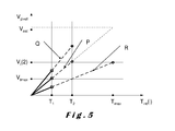
- FIG 4 shows a graph of pixel voltage, V pixel ' against integration time, T int ( i ) , that illustrates the process of optimum integration time prediction in three different pixels, "A", “B” and “C".
- V sat corresponds to the saturation voltage for each of pixels "A", “B” and “C”.
- the pixel voltages at T 1 , the shortest capture time, are indicated by V A , V B and Vc respectively.
- V pixelA , V pixelB and V pixelC respectively correspond to the pixel voltage at the predicted optimum integration time. As shown, for pixel "A”, the optimum integration time is T 1 ; for pixel "B”, T 2 ; and for pixel "C”, T max .
- V sat the pixel saturation voltage
- V t (1) the voltage of "A"
- V t (2) the voltage of "A”
- V t (2) is 50% of the saturation voltage
- V t (2) is 0.5V.
- V A (1) is higher than V t (2), thus T 1 is the best integration time for "A".
- Figure 5 illustrates an example of a pixel with a measured voltage close to the lowest reference value, V t max , affected by offset.
- P represents the real value
- Q represents the upper and lower offset levels respectively.
- the best integration time for "P” is T 2 .
- the upper offset value, "Q” causes the choice of a lower integration time, resulting in a slight reduction of SNR, for example, a SNR loss of between 0 and 3db.
- the lower offset value "R” on the contrary, can increase the predicted integration time, resulting in pixel saturation, as indicated by the dot-dash line.
- the pixel voltage which causes the reference value to be increased is estimated; and then the reference value is lowered by the amount of the estimated offset.
- the reference values can further be decreased without decreasing the SNR considerably. For example, a 50% reduction of the lowest reference value would result in a 3dB loss of the maximum SNR obtainable at that integration time. This is beneficial in the case of slight variability of light values during the integration period.
- T max the total integration time which is the sum of all the capture times needed for a determined DR and the relative processing times.
- T max the total integration time
- T frame the total integration time
- T 6 is 50% of T max (16ms)
- T 5 is 25% of T max (8ms)
- T 4 is 12.5% of T max (4ms)
- T 3 is 6.25% of T max (2ms)
- T 2 is 3.125% of T max (1 ms)
- T 1 is 1.6625% of T max (0.5ms).
- T frame ' the total integration time, T frame ' would be given by T max + T 1 , that is, 32.5ms which corresponds to a FR of 30.7 frames/s, that is, around double the frame rate of conventional MCT.
- the integration time for low-light detection is not compromised as T frame ⁇ T max if the first integration time is chosen to be very small compared to the maximum integration time.
- only the second capture is digitised providing substantial power reduction when compared to conventional MCT.
- Another advantage is the drop of power consumption required as only two captures are processed instead of n captures required by MCT.
- the advantages of the method of the present invention reside in the fact that an almost flat SNR characteristic is obtained at mid- and high-light (SNR dips of 3dB) without compromising the SNR at low-light.
- the present invention can be used with both destructive and non-destructive pixel readout systems, it is particularly useful with destructive pixel readout systems as there is a need to ensure that each pixel does not saturate in a particular frame.
- destructive pixel readout systems there is no need to predict as the charge on the pixels can be read without having to transfer the charge and therefore destroy the charge on each pixel.
Landscapes
- Engineering & Computer Science (AREA)
- Multimedia (AREA)
- Signal Processing (AREA)
- Transforming Light Signals Into Electric Signals (AREA)
- Solid State Image Pick-Up Elements (AREA)
Abstract
Description
- The present invention relates to improvements in dynamic range enhancement and is more particularly concerned with dynamic range enhancement through prediction of pixel integration time.
- Dynamic range (DR) is one of the most important features of imaging sensors as it provides the ability of a detector to capture highlights and shadows in the same frame. It is determined in accordance with the quality of the elements used to make the imaging sensor, that is, the quality of the pixels. In video systems, the dark-to-light contrast, in the same frame, is typically limited to between 60 and 70dB. This range is low compared to the dark-to-light contrast that can be obtained with the human eye.
- In such video systems, there is a need to have high signal-to-noise ratio (SNR) values over the whole range of operation of the pixels forming the imaging array without loss in image quality or increase in processing resources. Several methods are used to increase the dynamic range of an imaging sensor, for example, logarithmic pixel response, lateral overflow, multiple captures, etc.
- Logarithmic pixel response can provide a simple pixel architecture through which high DR can be obtained. Such a method of increasing DR is described in "Wide-Dynamic-Range CMOS Image Sensors ― Comparative Performance Analysis" by A Spivak, A Belenky, A Fish, and O Yadid-Pecht, Electron Devices, IEEE Transactions, pages 2446 to 2461, 2009.
- However, large noise at low light and image lag are clear disadvantages which are mainly exhibited in the sub-threshold operation where the diffusion current of the transistor is dominant. Furthermore variations of fabrication process parameters increase the fixed pattern noise.
- The lateral overflow method collects the charges generated by a high luminance in an extra capacitor as described by S Sugawa, N Akahane, S Adachi, K Mori, T lshiuchi and K Mizobuchi in "A 100dB Dynamic Range CMOS Image Sensor using a Lateral Overflow Integration Capacitor", Solid-State Circuits Conference, Digest of Technical Papers, ISSCC 2005 IEEE International, . This technique introduces a signal-to-noise ratio (SNR) dip at mid-light which degrades the performance of the sensor once the required DR becomes high, that is, more than 100dB. This is due to the switching between the high conversion gain of the floating diffusion node and the low conversion gain of the lateral overflow capacitor.
- A multiple captures techniques (MCT) method is described in "A 640 x 512 CMOS Image Sensor with Ultra Wide Dynamic Range Floating-Point Pixel-Level ADC" by DXD Yang, A El Gamal, B Fowler and Hui Tian, Solid-State Circuits Conference, Digest of Technical Papers, ISSCC 1999 IEEE International, pages 308 to 309, 1999. MCT allows wide dynamic range imaging by capturing images using different integration times and choosing the value closest to saturation. However, this technique requires a large total frame acquisition time, Tframe , which can be defined as:
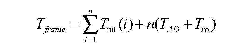
where n represents the number of captures needed for a certain DR;
Timt(i) represents the integration time of a capture "i";
TAD represents the analogue-to-digital (AD) conversion time; and
Tro represents the pixel readout time. - Furthermore, the multiple AD conversions needed per pixel, typically, one for each capture, and the image processing required to reconstruct the final image increase the overall power consumption of the imaging sensor.
- In order to reduce Tframe , a dual capture technique could be used which has a DR enhancement or extension, DR ext' defined by:

but with a SNR dip, SNRdip , defined by:
where T max represents the long capture time and T min represents the short capture time. However, for a dual capture process where the second capture time is chosen according to the required DR enhancement or extension, the consequent SNR dip would decrese the image quality at mid-light levels. This means that the DR enhancement or extension obtained depends on the maximum SNR dip in accordance with the specific application. - If a lower SNR dip is required, more captures with integration times within the range between T min and T max must be performed. This places a greater demand on resources with a lower frame rate and higher power consumption. For example, if an imaging sensor comprises a plurality of pixels that provide a DR of 60dB and it is desired to increase the DR to 120dB, ten extra captures are needed to provide a DR enhancement or extension of 60dB, where each capture provides an extra 6dB.
- It is therefore an object of the present invention to provide a method for extending the dynamic range of an image sensor whilst overcoming the disadvantages of SNR dip when using a dual capture process.
- It is a further object of the present invention to provide a method which makes it possible to improve the dynamic range of an imaging sensor by controlling the integration time of each pixel of the imaging sensor using a first short capture to estimate the optimal integration time for the pixel.
- In accordance with a first aspect of the present invention, there is provided a method of increasing the dynamic range of at least one pixel in a pixel array, the method comprising the steps of:
- a) determining a pixel output electrical value for each pixel after a predetermined integration time; and
- b) comparing the determined pixel output electrical value for each pixel with a set of reference values to determine an optimum integration time for each pixel in the pixel array;
characterised in that step b) comprises determining the set of reference values from one of: a pixel saturation electrical value and a pixel output electrical swing value for each pixel in the pixel array. - By determining an optimum integration time, the dynamic range of each pixel in the pixel array can be extended without the necessity of having to take many captures. In a preferred embodiment of the present invention, only two captures are required, that is, the capture at the predetermined integration time and the capture at the optimum integration time. This leads to a reduction in both processing time and processing power. In addition, frame rate is not substantially compromised as only two of captures need to be taken.
- Preferably, step b) further comprises the step of predicting the optimum integration time for each pixel in the pixel array in accordance with the comparison between the determined electrical value and the set of reference values.
- Moreover, it is preferred that step b) comprises setting the set of reference values as fractional multiples of the saturation electrical value. This means that, by knowing the nominal saturation electrical value of each pixel, it is possible to set a number of reference values which assist in the determination of the optimum integration time.
- In one embodiment of the present invention, the set of reference values has values:-

where Vt(i) is the ¡ 4th sub-threshold voltage within the saturation electrical value (Vsat) range. - Alternatively, step b) may comprise setting the set of reference values as fractional multiples of the pixel output electrical swing value, Vswing. In this case, the set of reference values has values:-

where Vt(i) is the i th sub-threshold voltage within the output electrical swing value range. - Step a) preferably comprises determining the predetermined integration time in accordance with:

where Tint(i) is a sub-interval integration time, Tmax is the maximum integration time of a frame, and n is the number of sub-integration intervals. - This means that the optimum integration time is Tint(i) when the electrical value (Vc1) is between Vt(i) and Vt(i+1), and Tmax when the electrical value (Vc1 ) is lower than Vt(n) where n is the number of sub-integration intervals.
- Advantageously, the method may further comprise the steps of c) estimating an offset for each pixel when the electrical value of each pixel causes the integration time thereof to be increased; and d) lowering the integration time of each pixel in accordance with the estimated offset.
- Additionally, the method may further comprise the step of adjusting for variability in light values by reducing the values of the set of reference values.
- After determining the optimum integration time for each pixel, the method preferably further comprises the step e) of reading out an electrical value from each pixel in accordance with the actual integration time. Step e) may comprise destructively reading out the electrical value or non-destructively reading out the electrical value.
- In another embodiment of the present invention, the method further comprises performing steps a) to e) for a group of pixels within the imaging array. In this way, an optimum integration time for the group of pixels can be predicted.
- For a better understanding of the present invention, reference will now be made, by way of example only, to the accompanying drawings in which:-
-
Figure 1 illustrates a graph of a typical SNR characteristic of a conventional imaging sensor illustrating the SNR dip when DR enhancement is applied; -
Figure 2 is similar toFigure 1 but showing three integration periods; -
Figure 3 illustrates a flow chart of a possible implementation of the method in accordance with the present invention; -
Figure 4 illustrates a graph of pixel integration times for three pixels with different electrical output values; and -
Figure 5 is similar toFigure 4 but illustrating the effect of offset in the prediction of the integration time. - The present invention will be described with respect to particular embodiments and with reference to certain drawings but the invention is not limited thereto. The drawings described are only schematic and are non-limiting. In the drawings, the size of some of the elements may be exaggerated and not drawn on scale for illustrative purposes.
- It will be understood that the terms "vertical" and "horizontal" are used herein refer to particular orientations of the Figures and these terms are not limitations to the specific embodiments described herein.
- In applications using imaging sensors, it is known to apply a number of threshold values to signals generated by pixels in the imaging sensor to control the operation of the particular application.
US-B-6995801 describes an imaging system in which the integration values are compared to upper and lower threshold values to control the imaging system. If the integration value is below the lower threshold value, an acceleration signal is generated. If the integration value is above the upper threshold value, a suppression signal is generated. If the integration value falls between the upper and lower threshold values, a fixed exposure signal is generated. The acceleration, suppression and fixed exposure signals are used to control the integration times of the imaging system. -
US-A-5793422 andEP-A-0583143 relate to electronic shutter control in video cameras. In both cases, the output of a low pass filter is compared to different threshold values to control the iris for the video camera. InEP-A-0583143 , the exposure time of the imaging sensor is controlled in accordance with a comparison between an output signal corresponding to the charges generated by the imaging sensor and a number of reference levels. InUS-A-5793422 , upper and lower reference levels bound a dead zone, the reference levels being controlled in accordance with the exposure time by increasing an absolute difference between the upper and lower reference levels as the exposure time decreases. -
WO-A-2009/073054 describes an imaging device in which the light induced charge for each pixel in a row is compared against a threshold level to determine whether or not to reset the pixels in the row as a result of the comparison. - None of
US-B-6995801 ,US-A-5793422 ,EP-A-0583143 orWO-A-2009/073054 discloses using a threshold level comparison to adjust and control the integration time of each pixel in an imaging array or imaging sensor. - The core element of the method of the present invention is the prediction of the optimum integration time for a single pixel or a group of pixels. For simplicity, the situation relating to a single pixel and its integration time will be described but it will readily be understood that the situation is also applicable to a group of pixels.
- In accordance with the present invention, only two captures at respective integration times are required. A first capture is made to predict the best integration time of the pixel or group of pixels. A second capture is made according to the optimum integration time predicted by the first capture. The higher the dynamic range required, the shorter the integration time needed for the first capture and the higher the advantages over the normal multiple captures technique.
- The term "wide dynamic range" as used herein is defined as the ratio of the brightest point of an image to the darkest point of the same image.
- The term "illuminance" as used herein is the total luminous flux incident on a surface, per unit area. It is a measure of the intensity of the incident light, wavelength-weighted by the luminosity function to correlate with human brightness perception.
- Referring initially to
Figure 1 , a typical SNR characteristic 100 of a sensor employing a lateral overflow technique is shown. The characteristic 100 comprises a graph of SNR against light intensity. Anormal sensor characteristic 110 is shown together with a characteristic 120 due to an overflow capacitor. As shown, the twocharacteristics final sensor characteristic 130, as shown by the solid line, with acertain SNR dip 140 which depends on the distance between the twocharacteristics characteristics - In order to understand the method of the present invention, the multiple captures technique (MCT) is explained first. The integration time, T, of a pixel is directly proportional to the charges it accumulates:

where Q is the amount of charge accumulated and I is the illuminance. - For high values of light intensity, a short integration time is required to avoid pixel saturation, that is, the point at which the pixel has reached the maximum charge it can collect. However, a short integration time also tends to limit the charge accumulated if the light level is low. This results in low SNR or even an unrecognisable light signal. To increase the dynamic range without affecting the low light detection, a MCT can be implemented. Each integration time can be chosen to be the double of the previous one so that if the shortest integration time is T1 then T2 will be 2T1, T3 will be 2T2, etc.
-
Figure 2 illustrates thetypical characteristic 200 of a sensor integrating three times. (The scale ofFigure 2 is different to that ofFigure 1 .) In this example of a MCT with three captures, the final SNR characteristic 210 is obtained by the overlapping of each capture SNR characteristic, that is, thenormal DR 230 and two overlapping characteristics to provide theDR extension 240. ASNR dip 250 is still obtained. If each subsequent integration time is double the previous one, the enhanced DR obtained is 6dB per extra capture and the SNR dip is 3dB. For simplicity, the electrical output signal of the pixels is assumed to increase as the light intensity increases. - After each integration period, the electrical value of the pixel, for example, its voltage, is compared with a reference voltage value. This reference voltage value is usually half of the full voltage range of the pixel, that is, its saturation voltage. Here, the voltage value is used as the pixel electrical value, but it will be appreciated that other representations of the pixel electrical value can be used.
- If the voltage value measured is above this reference value, that is, 50% of the full range of the pixel then the voltage of the pixel and the corresponding integration time are digitised. Each capture time corresponds to a left shifting of the digitised pixel value. For example, if the resolution of an analogue-to-digital converter (ADC) is 8-bit and the number of extra captures is 10, then the virtual resolution of the pixel will be 18 bits. If the chosen integration time is T1, that is, the shortest integration time, the fine pixel conversion of 8-bit is shifted left to the most significant bit. There will be, in this case, a truncation of the 10 least significant bits. This truncation does not, however, compromise the SNR of the pixel because at high light intensity values, the dominant noise is usually the photon shot noise rather than the ADC noise.
- The extension of dynamic range obtained with MCT corresponds to 6dB for each extra integration time or period. If a basic sensor provides 60dB of DR, 10 extra captures are needed to extend the DR to 120dB.
- On the contrary, the method in accordance with the present invention integrates only twice for each pixel. The first integration comprises a short integration time which is used to predict an optimum value for the second integration time. In order to limit the processing complexity and to reduce the number of SNR dips as shown in
Figure 2 , the total integration time can be divided into sub-integration times, T¡nt (i) , where each T int(i) is chosen according to:
with T max representing the maximum integration time of the frame, n is the number of captures needed for a certain DR enhancement, and "n―1" is the number of bits encoding the DR enhancement. -
Figure 3 illustrates aflow chart 300 showing an implementation of the method of DR enhancement or extension in accordance with the present invention. The first step,step 305, is to take the first capture with the shortest integration time, T int (1) , and to store the voltage, Vc1, relating to this first capture,step 310. The first capture is used to predict the optimum value for the second integration time. The prediction is based on the comparison of the stored voltage corresponding to the first capture, V cl, with a reference value, Vt (i), which is obtained as follows:
where Vsat represents the saturation voltage of the pixel. During a second capture,step 315, before each T¡nt (i), V cl, is compared to Vt (i+1). For the first interval, T int (1) , the comparison V c1>Vt (2) is made,step 320. If V c1>V t(2), the capture is made at t = T int (1) instep 325. The voltage read is stored in a sample-and-hold (S&H) circuit, the mantissa bit is sent for storage in a digital memory in order to perform a floating point DR extension,step 330, and a "veto" signal is sent back to the pixel to avoid further integrations within the same frame. - If V c1<V t(2), a second comparison is made in
step 340 where V c1 is compared to a second lower threshold value, Vt (3). If V c1>Vt (3), a capture is made at t = T int(2) ,step 345, and the voltage read is stored in a S&H circuit, the mantissa bit is sent for storage in the digital memory,step 350, and a "veto" signal is sent back to the pixel to avoid further integrations within the same frame. - If V c1<Vt (3), the process is repeated until the i th comparison,
step 355. If V c1>Vt (i+1), a capture is made at t = T¡nt (i),step 360, and the voltage read is stored in a S&H circuit, the mantissa bit is sent for storage in the digital memory (step 365), and a "veto" signal is sent back to the pixel to avoid further integrations within the same frame. - If V c1<Vt (i+1), then the capture is made at t = T max ,
step 370, and the voltage read is stored in a S&H circuit, the mantissa bit is sent for storage in the digital memory (step 375). - At the end of the frame, the voltage corresponding to the predicted integration time is sent for analogue-to-digital conversion (ADC) in
step 335. - As an alternative to using the saturation value as the basis for the set of reference values, a pixel output electrical swing value, Vswing, can be used. In this case, Vt (i) can be expressed as:

-
Figure 4 shows a graph of pixel voltage, Vpixel ' against integration time, T int(i), that illustrates the process of optimum integration time prediction in three different pixels, "A", "B" and "C". For simplicity, only three reference values are used in this example resulting in a DR extension of 12dB. (This corresponds to the requirement for three captures in MCT to obtain a DR enhancement or extension of 12dB.) Vsat corresponds to the saturation voltage for each of pixels "A", "B" and "C". The pixel voltages at T 1, the shortest capture time, are indicated by VA, VB and Vc respectively. VpixelA, VpixelB and VpixelC respectively correspond to the pixel voltage at the predicted optimum integration time. As shown, for pixel "A", the optimum integration time is T 1; for pixel "B", T 2; and for pixel "C", T max . - Here, it is assumed that the pixel saturation voltage, Vsat , which also corresponds to Vt (1), is 1V. After the shortest capture time, T 1, the voltage of "A", V A(1), is compared to a first threshold value, Vt (2), which is 50% of the saturation voltage, Vsat . In this example, Vt (2) is 0.5V. As shown in
Figure 4 , VA (1) is higher than Vt (2), thus T 1 is the best integration time for "A". - In the case of "B", a first comparison is done again to 0.5V. Since the voltage of "B", VB (1), is lower than Vt (2), the next reference value, V tmax (which corresponds to Vt (3)), in this case, 0.25V is tried. As VB (1) is higher than V tmax, the best integration time for "B" is T 2.
- For "C", a comparison is also made with Vt (2) (0.5V) and V tmax (0.25V). However, the voltage of "C", VC (1) , is lower than both Vt (2) and V tmax. Therefore, the best integration time for "C" is the longest one, T max,
- If the voltage of the pixel at the time of comparison is very close to one of the reference values, noise and offset at pixel and peripheral circuitry can compromise the prediction of the best integration time. This results, in the worse case, in the choice a longer integration time than the optimum value, causing pixel saturation.
-
Figure 5 illustrates an example of a pixel with a measured voltage close to the lowest reference value, V tmax, affected by offset. "P" represents the real value, whilst "Q" and "R" include the upper and lower offset levels respectively. The best integration time for "P" is T 2. The upper offset value, "Q", causes the choice of a lower integration time, resulting in a slight reduction of SNR, for example, a SNR loss of between 0 and 3db. The lower offset value "R", on the contrary, can increase the predicted integration time, resulting in pixel saturation, as indicated by the dot-dash line. - In order to solve the issue of pixel offset, the pixel voltage which causes the reference value to be increased is estimated; and then the reference value is lowered by the amount of the estimated offset.
- The reference values can further be decreased without decreasing the SNR considerably. For example, a 50% reduction of the lowest reference value would result in a 3dB loss of the maximum SNR obtainable at that integration time. This is beneficial in the case of slight variability of light values during the integration period.
- By using the dual capture method for DR extension or enhancement as described above, most of the advantages of MCT can be obtained, such as, linear light to voltage conversion, same SNR at low light of a conventional pixel, low SNR dips at mid- and high-light (-3dB if each integration time is chosen to be twice that of the previous one as given above).
- However, MCT needs a total integration time which is the sum of all the capture times needed for a determined DR and the relative processing times. As an example, for a pixel which requires an integration time, T max, of 32ms in order to detect low-light at a predetermined level, and if the DR enhancement or extension required corresponds to 30dB, 6 extra captures are required. This results in a total integration time, Tframe , of:

- This equates to a value of 63.5ms where T 6 is 50% of T max (16ms), T 5 is 25% of T max (8ms), T 4 is 12.5% of T max (4ms), T 3 is 6.25% of T max (2ms), T 2 is 3.125% of T max (1 ms) and T 1 is 1.6625% of T max (0.5ms). This means that if the sensor is used to capture videos, the maximum frame rate (FR) would be limited to 15.7 frames/s.
- In comparison, if the method of the present invention is used, the total integration time, T frame' would be given by Tmax + T 1 , that is, 32.5ms which corresponds to a FR of 30.7 frames/s, that is, around double the frame rate of conventional MCT.
- In addition, the integration time for low-light detection is not compromised as Tframe ∼ T max if the first integration time is chosen to be very small compared to the maximum integration time. Moreover, only the second capture is digitised providing substantial power reduction when compared to conventional MCT.
- Another advantage is the drop of power consumption required as only two captures are processed instead of n captures required by MCT.
- Compared to other DR extension or enhancement techniques, the advantages of the method of the present invention reside in the fact that an almost flat SNR characteristic is obtained at mid- and high-light (SNR dips of 3dB) without compromising the SNR at low-light.
- Whilst the present invention can be used with both destructive and non-destructive pixel readout systems, it is particularly useful with destructive pixel readout systems as there is a need to ensure that each pixel does not saturate in a particular frame. For non-destructive pixel readout systems, there is no need to predict as the charge on the pixels can be read without having to transfer the charge and therefore destroy the charge on each pixel.
Claims (15)
- A method of increasing the dynamic range of at least one pixel in a pixel array, the method comprising the steps of:a) determining an electrical pixel output value (Vc1 ) for each pixel after a predetermined integration time (T1 ); andb) comparing the determined pixel output electrical value (Vc1 ) for each pixel with a set of reference values (Vt(i)) to determine an optimum integration time for each pixel in the pixel array;
characterised in that step b) comprises determining the set of reference values (Vt(i)) from one of: a pixel saturation electrical value (Vsat) and a pixel output electrical swing value (Vswing) for each pixel in the pixel array. - A method according to claim 1, wherein step b) further comprises the step of predicting the optimum integration time for each pixel in the pixel array in accordance with the comparison between the determined electrical value (Vc1 ) and the set of reference values (Vt (i)).
- A method according to claim 1 or 2, wherein step b) comprises setting the set of reference values (Vt(i)) as fractional multiples of the pixel saturation electrical value (Vsat).
- A method according to claim 3, wherein the set of reference values has values:-

where Vt(i) is the i th sub-threshold voltage within the saturation electrical value (Vsat ) range. - A method according to claim 1 or 2, wherein step b) comprises setting the set of reference values (Vt (i)) as fractional multiples of the pixel output electrical swing value (Vswing ).
- A method according to claim 5, wherein the set of reference values has values:-
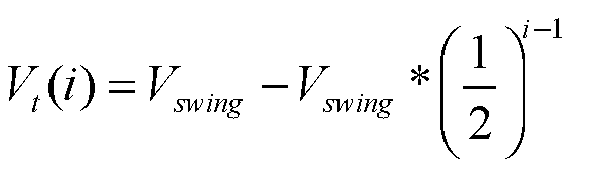
where Vt (i) is the i th sub-threshold voltage within the output electrical swing value (Vswing ) range. - A method according to any one of the preceding claims, wherein step a) comprises determining the predetermined integration time (T1 ) in accordance with:

where Tint (i) is a sub-interval integration time, Tmax is the maximum integration time of a frame, and n is the number of sub-integration intervals. - A method according to any one of the preceding claims, wherein the optimum integration time is Tint (i) when the electrical value (Vc1 ) is between Vt (i) and Vt (i+1).
- A method according to any one of claims 1 to 7, wherein the optimum integration time is Tmax when the electrical value (Vc1 ) is lower than Vt (n) where n is the number of sub-integration intervals.
- A method according to any one of the preceding claims, further comprising the steps of:c) estimating an offset for each pixel when the electrical value of each pixel causes the integration time thereof to be increased; andd) lowering the integration time of each pixel in accordance with the estimated offset.
- A method according to any one of the preceding claims, further comprising the step of adjusting for variability in light values by reducing the values of the set of reference values (Vt (i)).
- A method according to any one of the preceding claims, further comprising the step e) of reading out an electrical value from each pixel in accordance with the optimum integration time.
- A method according to claim 12, wherein step e) comprises destructively reading out the electrical value.
- A method according to claim 12, wherein step e) comprises non-destructively reading out the electrical value.
- A method according to any one of the preceding claims, further comprising performing steps a) to e) for a group of pixels within the pixel array.
Applications Claiming Priority (1)
| Application Number | Priority Date | Filing Date | Title |
|---|---|---|---|
| GBGB1016773.2A GB201016773D0 (en) | 2010-10-06 | 2010-10-06 | Dynamic range enhancement through prediction of pixel integration time |
Publications (3)
| Publication Number | Publication Date |
|---|---|
| EP2439930A2 true EP2439930A2 (en) | 2012-04-11 |
| EP2439930A3 EP2439930A3 (en) | 2012-06-13 |
| EP2439930B1 EP2439930B1 (en) | 2018-12-05 |
Family
ID=43243556
Family Applications (1)
| Application Number | Title | Priority Date | Filing Date |
|---|---|---|---|
| EP11184117.7A Active EP2439930B1 (en) | 2010-10-06 | 2011-10-06 | Improvements in or relating to dynamic range enhancement of imaging sensors |
Country Status (3)
| Country | Link |
|---|---|
| US (1) | US8792032B2 (en) |
| EP (1) | EP2439930B1 (en) |
| GB (1) | GB201016773D0 (en) |
Cited By (1)
| Publication number | Priority date | Publication date | Assignee | Title |
|---|---|---|---|---|
| EP3226547A1 (en) * | 2016-03-31 | 2017-10-04 | STMicroelectronics (Research & Development) Limited | Controlling signal-to-noise ratio in high dynamic range automatic exposure control imaging |
Families Citing this family (5)
| Publication number | Priority date | Publication date | Assignee | Title |
|---|---|---|---|---|
| GB2497571A (en) * | 2011-12-15 | 2013-06-19 | St Microelectronics Res & Dev | An imaging array with high dynamic range |
| JP2013183434A (en) * | 2012-03-05 | 2013-09-12 | Toshiba Corp | Solid-state imaging apparatus |
| CN104160695B (en) * | 2012-03-09 | 2017-04-26 | 富士胶片株式会社 | Radiography device, radiography system, and radiography device control method |
| US9319605B2 (en) * | 2013-03-15 | 2016-04-19 | Rambus Inc. | Increasing dynamic range using multisampling |
| US9866770B2 (en) * | 2015-10-21 | 2018-01-09 | Massachusetts Institute Of Technology | Methods and apparatus for true high dynamic range (THDR) time-delay-and-integrate (TDI) imaging |
Citations (3)
| Publication number | Priority date | Publication date | Assignee | Title |
|---|---|---|---|---|
| EP0583143A2 (en) | 1992-08-10 | 1994-02-16 | Sony Corporation | Improved control of the electronic shutter time in a video camera |
| US6995801B1 (en) | 1999-02-08 | 2006-02-07 | Sanyo Electric Co., Ltd. | Method and apparatus for controlling an exposure period of a solid-state imaging apparatus based upon an image signal output |
| WO2009073054A1 (en) | 2007-12-06 | 2009-06-11 | Gentex Corporation | Improved imaging device |
Family Cites Families (6)
| Publication number | Priority date | Publication date | Assignee | Title |
|---|---|---|---|---|
| IL155046A (en) * | 2003-03-23 | 2013-12-31 | Given Imaging Ltd | In-vivo imaging device capable of defining its location |
| US7492400B2 (en) * | 2004-06-01 | 2009-02-17 | The Board Of Trustees Of The Leland Stanford Junior University | Adaptive pixel for high dynamic range and disturbance detection and correction |
| EP1829364A2 (en) * | 2004-12-07 | 2007-09-05 | Bright Imaging Ltd. | Method and apparatus for imaging of scenes having large intensity variance |
| JP4998056B2 (en) * | 2006-05-11 | 2012-08-15 | セイコーエプソン株式会社 | Imaging apparatus, imaging system, and imaging method |
| US7969490B2 (en) * | 2006-08-25 | 2011-06-28 | Micron Technology, Inc. | Method, apparatus, and system providing an imager with pixels having extended dynamic range |
| US7791657B2 (en) * | 2007-03-07 | 2010-09-07 | Teledyne Licensing, Llc | Dynamic range enhancement scheme for imagers |
-
2010
- 2010-10-06 GB GBGB1016773.2A patent/GB201016773D0/en not_active Ceased
-
2011
- 2011-10-06 US US13/267,797 patent/US8792032B2/en active Active
- 2011-10-06 EP EP11184117.7A patent/EP2439930B1/en active Active
Patent Citations (4)
| Publication number | Priority date | Publication date | Assignee | Title |
|---|---|---|---|---|
| EP0583143A2 (en) | 1992-08-10 | 1994-02-16 | Sony Corporation | Improved control of the electronic shutter time in a video camera |
| US5793422A (en) | 1992-08-10 | 1998-08-11 | Sony Corporation | Electron shutter control with exposure control responsive to shutter gain differences |
| US6995801B1 (en) | 1999-02-08 | 2006-02-07 | Sanyo Electric Co., Ltd. | Method and apparatus for controlling an exposure period of a solid-state imaging apparatus based upon an image signal output |
| WO2009073054A1 (en) | 2007-12-06 | 2009-06-11 | Gentex Corporation | Improved imaging device |
Non-Patent Citations (3)
| Title |
|---|
| A SPIVAK, A BELENKY, A FISH, 0 YADID-PECHT: "Wide-Dynamic-Range CMOS Image Sensors - Comparative Performance Analysis", ELECTRON DEVICES, IEEE TRANSACTIONS, 2009, pages 2446 - 2461, XP011277607, DOI: doi:10.1109/TED.2009.2030599 |
| DXD YANG, A EI GAMAL, B FOWLER, HUI TIAN: "A 640 x 512 CMOS Image Sensor with Ultra Wide Dynamic Range Floating-Point Pixel-Level ADC", SOLID-STATE CIRCUITS CONFERENCE, DIGEST OF TECHNICAL PAPERS, ISSCC 1999, 1999, pages 308 - 309 |
| S SUGAWA, N AKAHANE, S ADACHI, K MORI, T ISHIUCHI, K MIZOBUCHI: "A 100dB Dynamic Range CMOS Image Sensor using a Lateral Overflow Integration Capacitor", SOLID-STATE CIRCUITS CONFERENCE, DIGEST OF TECHNICAL PAPERS, ISSCC 2005 IEEE INTERNATIONAL, vol. 1, 2005, pages 352 - 603, XP002588739 |
Cited By (2)
| Publication number | Priority date | Publication date | Assignee | Title |
|---|---|---|---|---|
| EP3226547A1 (en) * | 2016-03-31 | 2017-10-04 | STMicroelectronics (Research & Development) Limited | Controlling signal-to-noise ratio in high dynamic range automatic exposure control imaging |
| US9787909B1 (en) | 2016-03-31 | 2017-10-10 | Stmicroelectronics (Research & Development) Limited | Controlling signal-to-noise ratio in high dynamic range automatic exposure control imaging |
Also Published As
| Publication number | Publication date |
|---|---|
| US8792032B2 (en) | 2014-07-29 |
| US20120086840A1 (en) | 2012-04-12 |
| EP2439930B1 (en) | 2018-12-05 |
| GB201016773D0 (en) | 2010-11-17 |
| EP2439930A3 (en) | 2012-06-13 |
Similar Documents
| Publication | Publication Date | Title |
|---|---|---|
| US12231788B2 (en) | Method, apparatus, and system providing an imager with pixels having extended dynamic range | |
| EP3036894B1 (en) | System and method for capturing images with multiple image sensing elements | |
| US7796171B2 (en) | Sensor-based gamma correction of a digital camera | |
| US8368792B2 (en) | Imager methods, apparatuses, and systems providing a skip mode with a wide dynamic range operation | |
| US8681265B2 (en) | Imaging device, external flash detection method, program, and integrated circuit | |
| JP3976754B2 (en) | Wide dynamic range imaging device with selective reading | |
| US8643755B2 (en) | Solid-state imaging device and camera system | |
| JP5223953B2 (en) | Solid-state imaging device, driving method of solid-state imaging device, and imaging device | |
| EP2439930B1 (en) | Improvements in or relating to dynamic range enhancement of imaging sensors | |
| US20080198251A1 (en) | Method, apparatus, and system providing multiple pixel integration periods | |
| US8749685B2 (en) | Solid-state imaging device, driving method thereof, and imaging apparatus | |
| JP2007151069A (en) | Solid-state imaging device, driving method of solid-state imaging device, and imaging device | |
| US8144215B2 (en) | Method and apparatus of using processor with analog-to-digital converter within image sensor to achieve high dynamic range of image sensor | |
| JP5569298B2 (en) | Image processing apparatus, image processing method, and program | |
| US12022222B2 (en) | CMOS image sensor pixel array and readout method with LED flicker mitigation | |
| US10498972B1 (en) | High-dynamic-range imaging system and method | |
| WO2016203966A1 (en) | Imaging device, imaging method, and program | |
| CN106454159A (en) | High-dynamic EMCCD (Electronic Multiplying CCD) image sensor | |
| US20250280211A1 (en) | Imaging device | |
| JP4872502B2 (en) | Imaging apparatus and clamping method thereof | |
| JP2005304009A (en) | Voltage control device of charge coupled device | |
| JP2006197229A (en) | Imaging device and camera | |
| Seliuchenko et al. | Partial reset HDR image sensor with improved fixed pattern noise performance | |
| KR20140136287A (en) | Imaging device and method for driving thereof |
Legal Events
| Date | Code | Title | Description |
|---|---|---|---|
| AK | Designated contracting states |
Kind code of ref document: A2 Designated state(s): AL AT BE BG CH CY CZ DE DK EE ES FI FR GB GR HR HU IE IS IT LI LT LU LV MC MK MT NL NO PL PT RO RS SE SI SK SM TR |
|
| AX | Request for extension of the european patent |
Extension state: BA ME |
|
| PUAI | Public reference made under article 153(3) epc to a published international application that has entered the european phase |
Free format text: ORIGINAL CODE: 0009012 |
|
| PUAL | Search report despatched |
Free format text: ORIGINAL CODE: 0009013 |
|
| AK | Designated contracting states |
Kind code of ref document: A3 Designated state(s): AL AT BE BG CH CY CZ DE DK EE ES FI FR GB GR HR HU IE IS IT LI LT LU LV MC MK MT NL NO PL PT RO RS SE SI SK SM TR |
|
| AX | Request for extension of the european patent |
Extension state: BA ME |
|
| RIC1 | Information provided on ipc code assigned before grant |
Ipc: H04N 5/355 20110101AFI20120508BHEP Ipc: H04N 5/235 20060101ALI20120508BHEP |
|
| RIN1 | Information on inventor provided before grant (corrected) |
Inventor name: XHAKONI, ADI Inventor name: GIELEN, GEORGES Inventor name: SAN SEGUNDO BELLO, DAVID |
|
| 17P | Request for examination filed |
Effective date: 20121213 |
|
| STAA | Information on the status of an ep patent application or granted ep patent |
Free format text: STATUS: EXAMINATION IS IN PROGRESS |
|
| 17Q | First examination report despatched |
Effective date: 20171016 |
|
| RAP1 | Party data changed (applicant data changed or rights of an application transferred) |
Owner name: IMEC VZW Owner name: KATHOLIEKE UNIVERSITEIT LEUVEN, K.U. LEUVEN R&D |
|
| GRAP | Despatch of communication of intention to grant a patent |
Free format text: ORIGINAL CODE: EPIDOSNIGR1 |
|
| STAA | Information on the status of an ep patent application or granted ep patent |
Free format text: STATUS: GRANT OF PATENT IS INTENDED |
|
| INTG | Intention to grant announced |
Effective date: 20180530 |
|
| GRAS | Grant fee paid |
Free format text: ORIGINAL CODE: EPIDOSNIGR3 |
|
| RAP1 | Party data changed (applicant data changed or rights of an application transferred) |
Owner name: IMEC VZW Owner name: KATHOLIEKE UNIVERSITEIT LEUVEN |
|
| RIN1 | Information on inventor provided before grant (corrected) |
Inventor name: XHAKONI, ADI Inventor name: SAN SEGUNDO BELLO, DAVID Inventor name: GIELEN, GEORGES |
|
| GRAA | (expected) grant |
Free format text: ORIGINAL CODE: 0009210 |
|
| GRAA | (expected) grant |
Free format text: ORIGINAL CODE: 0009210 |
|
| STAA | Information on the status of an ep patent application or granted ep patent |
Free format text: STATUS: THE PATENT HAS BEEN GRANTED |
|
| AK | Designated contracting states |
Kind code of ref document: B1 Designated state(s): AL AT BE BG CH CY CZ DE DK EE ES FI FR GB GR HR HU IE IS IT LI LT LU LV MC MK MT NL NO PL PT RO RS SE SI SK SM TR |
|
| REG | Reference to a national code |
Ref country code: GB Ref legal event code: FG4D |
|
| REG | Reference to a national code |
Ref country code: CH Ref legal event code: EP |
|
| REG | Reference to a national code |
Ref country code: AT Ref legal event code: REF Ref document number: 1074564 Country of ref document: AT Kind code of ref document: T Effective date: 20181215 |
|
| REG | Reference to a national code |
Ref country code: IE Ref legal event code: FG4D |
|
| REG | Reference to a national code |
Ref country code: DE Ref legal event code: R096 Ref document number: 602011054459 Country of ref document: DE |
|
| REG | Reference to a national code |
Ref country code: NL Ref legal event code: MP Effective date: 20181205 |
|
| REG | Reference to a national code |
Ref country code: AT Ref legal event code: MK05 Ref document number: 1074564 Country of ref document: AT Kind code of ref document: T Effective date: 20181205 |
|
| REG | Reference to a national code |
Ref country code: LT Ref legal event code: MG4D |
|
| PG25 | Lapsed in a contracting state [announced via postgrant information from national office to epo] |
Ref country code: ES Free format text: LAPSE BECAUSE OF FAILURE TO SUBMIT A TRANSLATION OF THE DESCRIPTION OR TO PAY THE FEE WITHIN THE PRESCRIBED TIME-LIMIT Effective date: 20181205 Ref country code: AT Free format text: LAPSE BECAUSE OF FAILURE TO SUBMIT A TRANSLATION OF THE DESCRIPTION OR TO PAY THE FEE WITHIN THE PRESCRIBED TIME-LIMIT Effective date: 20181205 Ref country code: LT Free format text: LAPSE BECAUSE OF FAILURE TO SUBMIT A TRANSLATION OF THE DESCRIPTION OR TO PAY THE FEE WITHIN THE PRESCRIBED TIME-LIMIT Effective date: 20181205 Ref country code: HR Free format text: LAPSE BECAUSE OF FAILURE TO SUBMIT A TRANSLATION OF THE DESCRIPTION OR TO PAY THE FEE WITHIN THE PRESCRIBED TIME-LIMIT Effective date: 20181205 Ref country code: NO Free format text: LAPSE BECAUSE OF FAILURE TO SUBMIT A TRANSLATION OF THE DESCRIPTION OR TO PAY THE FEE WITHIN THE PRESCRIBED TIME-LIMIT Effective date: 20190305 Ref country code: BG Free format text: LAPSE BECAUSE OF FAILURE TO SUBMIT A TRANSLATION OF THE DESCRIPTION OR TO PAY THE FEE WITHIN THE PRESCRIBED TIME-LIMIT Effective date: 20190305 Ref country code: FI Free format text: LAPSE BECAUSE OF FAILURE TO SUBMIT A TRANSLATION OF THE DESCRIPTION OR TO PAY THE FEE WITHIN THE PRESCRIBED TIME-LIMIT Effective date: 20181205 Ref country code: LV Free format text: LAPSE BECAUSE OF FAILURE TO SUBMIT A TRANSLATION OF THE DESCRIPTION OR TO PAY THE FEE WITHIN THE PRESCRIBED TIME-LIMIT Effective date: 20181205 |
|
| PG25 | Lapsed in a contracting state [announced via postgrant information from national office to epo] |
Ref country code: SE Free format text: LAPSE BECAUSE OF FAILURE TO SUBMIT A TRANSLATION OF THE DESCRIPTION OR TO PAY THE FEE WITHIN THE PRESCRIBED TIME-LIMIT Effective date: 20181205 Ref country code: AL Free format text: LAPSE BECAUSE OF FAILURE TO SUBMIT A TRANSLATION OF THE DESCRIPTION OR TO PAY THE FEE WITHIN THE PRESCRIBED TIME-LIMIT Effective date: 20181205 Ref country code: RS Free format text: LAPSE BECAUSE OF FAILURE TO SUBMIT A TRANSLATION OF THE DESCRIPTION OR TO PAY THE FEE WITHIN THE PRESCRIBED TIME-LIMIT Effective date: 20181205 Ref country code: GR Free format text: LAPSE BECAUSE OF FAILURE TO SUBMIT A TRANSLATION OF THE DESCRIPTION OR TO PAY THE FEE WITHIN THE PRESCRIBED TIME-LIMIT Effective date: 20190306 |
|
| PG25 | Lapsed in a contracting state [announced via postgrant information from national office to epo] |
Ref country code: NL Free format text: LAPSE BECAUSE OF FAILURE TO SUBMIT A TRANSLATION OF THE DESCRIPTION OR TO PAY THE FEE WITHIN THE PRESCRIBED TIME-LIMIT Effective date: 20181205 |
|
| PG25 | Lapsed in a contracting state [announced via postgrant information from national office to epo] |
Ref country code: PT Free format text: LAPSE BECAUSE OF FAILURE TO SUBMIT A TRANSLATION OF THE DESCRIPTION OR TO PAY THE FEE WITHIN THE PRESCRIBED TIME-LIMIT Effective date: 20190405 Ref country code: CZ Free format text: LAPSE BECAUSE OF FAILURE TO SUBMIT A TRANSLATION OF THE DESCRIPTION OR TO PAY THE FEE WITHIN THE PRESCRIBED TIME-LIMIT Effective date: 20181205 Ref country code: PL Free format text: LAPSE BECAUSE OF FAILURE TO SUBMIT A TRANSLATION OF THE DESCRIPTION OR TO PAY THE FEE WITHIN THE PRESCRIBED TIME-LIMIT Effective date: 20181205 Ref country code: IT Free format text: LAPSE BECAUSE OF FAILURE TO SUBMIT A TRANSLATION OF THE DESCRIPTION OR TO PAY THE FEE WITHIN THE PRESCRIBED TIME-LIMIT Effective date: 20181205 |
|
| PG25 | Lapsed in a contracting state [announced via postgrant information from national office to epo] |
Ref country code: EE Free format text: LAPSE BECAUSE OF FAILURE TO SUBMIT A TRANSLATION OF THE DESCRIPTION OR TO PAY THE FEE WITHIN THE PRESCRIBED TIME-LIMIT Effective date: 20181205 Ref country code: SM Free format text: LAPSE BECAUSE OF FAILURE TO SUBMIT A TRANSLATION OF THE DESCRIPTION OR TO PAY THE FEE WITHIN THE PRESCRIBED TIME-LIMIT Effective date: 20181205 Ref country code: RO Free format text: LAPSE BECAUSE OF FAILURE TO SUBMIT A TRANSLATION OF THE DESCRIPTION OR TO PAY THE FEE WITHIN THE PRESCRIBED TIME-LIMIT Effective date: 20181205 Ref country code: IS Free format text: LAPSE BECAUSE OF FAILURE TO SUBMIT A TRANSLATION OF THE DESCRIPTION OR TO PAY THE FEE WITHIN THE PRESCRIBED TIME-LIMIT Effective date: 20190405 Ref country code: SK Free format text: LAPSE BECAUSE OF FAILURE TO SUBMIT A TRANSLATION OF THE DESCRIPTION OR TO PAY THE FEE WITHIN THE PRESCRIBED TIME-LIMIT Effective date: 20181205 |
|
| REG | Reference to a national code |
Ref country code: DE Ref legal event code: R097 Ref document number: 602011054459 Country of ref document: DE |
|
| PLBE | No opposition filed within time limit |
Free format text: ORIGINAL CODE: 0009261 |
|
| STAA | Information on the status of an ep patent application or granted ep patent |
Free format text: STATUS: NO OPPOSITION FILED WITHIN TIME LIMIT |
|
| PG25 | Lapsed in a contracting state [announced via postgrant information from national office to epo] |
Ref country code: DK Free format text: LAPSE BECAUSE OF FAILURE TO SUBMIT A TRANSLATION OF THE DESCRIPTION OR TO PAY THE FEE WITHIN THE PRESCRIBED TIME-LIMIT Effective date: 20181205 Ref country code: SI Free format text: LAPSE BECAUSE OF FAILURE TO SUBMIT A TRANSLATION OF THE DESCRIPTION OR TO PAY THE FEE WITHIN THE PRESCRIBED TIME-LIMIT Effective date: 20181205 |
|
| 26N | No opposition filed |
Effective date: 20190906 |
|
| PG25 | Lapsed in a contracting state [announced via postgrant information from national office to epo] |
Ref country code: TR Free format text: LAPSE BECAUSE OF FAILURE TO SUBMIT A TRANSLATION OF THE DESCRIPTION OR TO PAY THE FEE WITHIN THE PRESCRIBED TIME-LIMIT Effective date: 20181205 |
|
| PG25 | Lapsed in a contracting state [announced via postgrant information from national office to epo] |
Ref country code: MC Free format text: LAPSE BECAUSE OF FAILURE TO SUBMIT A TRANSLATION OF THE DESCRIPTION OR TO PAY THE FEE WITHIN THE PRESCRIBED TIME-LIMIT Effective date: 20181205 |
|
| REG | Reference to a national code |
Ref country code: CH Ref legal event code: PL |
|
| PG25 | Lapsed in a contracting state [announced via postgrant information from national office to epo] |
Ref country code: LU Free format text: LAPSE BECAUSE OF NON-PAYMENT OF DUE FEES Effective date: 20191006 Ref country code: CH Free format text: LAPSE BECAUSE OF NON-PAYMENT OF DUE FEES Effective date: 20191031 Ref country code: LI Free format text: LAPSE BECAUSE OF NON-PAYMENT OF DUE FEES Effective date: 20191031 |
|
| REG | Reference to a national code |
Ref country code: BE Ref legal event code: MM Effective date: 20191031 |
|
| PG25 | Lapsed in a contracting state [announced via postgrant information from national office to epo] |
Ref country code: BE Free format text: LAPSE BECAUSE OF NON-PAYMENT OF DUE FEES Effective date: 20191031 |
|
| PG25 | Lapsed in a contracting state [announced via postgrant information from national office to epo] |
Ref country code: IE Free format text: LAPSE BECAUSE OF NON-PAYMENT OF DUE FEES Effective date: 20191006 |
|
| PG25 | Lapsed in a contracting state [announced via postgrant information from national office to epo] |
Ref country code: CY Free format text: LAPSE BECAUSE OF FAILURE TO SUBMIT A TRANSLATION OF THE DESCRIPTION OR TO PAY THE FEE WITHIN THE PRESCRIBED TIME-LIMIT Effective date: 20181205 |
|
| PG25 | Lapsed in a contracting state [announced via postgrant information from national office to epo] |
Ref country code: MT Free format text: LAPSE BECAUSE OF FAILURE TO SUBMIT A TRANSLATION OF THE DESCRIPTION OR TO PAY THE FEE WITHIN THE PRESCRIBED TIME-LIMIT Effective date: 20181205 Ref country code: HU Free format text: LAPSE BECAUSE OF FAILURE TO SUBMIT A TRANSLATION OF THE DESCRIPTION OR TO PAY THE FEE WITHIN THE PRESCRIBED TIME-LIMIT; INVALID AB INITIO Effective date: 20111006 |
|
| PG25 | Lapsed in a contracting state [announced via postgrant information from national office to epo] |
Ref country code: MK Free format text: LAPSE BECAUSE OF FAILURE TO SUBMIT A TRANSLATION OF THE DESCRIPTION OR TO PAY THE FEE WITHIN THE PRESCRIBED TIME-LIMIT Effective date: 20181205 |
|
| REG | Reference to a national code |
Ref country code: DE Ref legal event code: R079 Ref document number: 602011054459 Country of ref document: DE Free format text: PREVIOUS MAIN CLASS: H04N0005355000 Ipc: H04N0025570000 |
|
| P01 | Opt-out of the competence of the unified patent court (upc) registered |
Effective date: 20230513 |
|
| PGFP | Annual fee paid to national office [announced via postgrant information from national office to epo] |
Ref country code: GB Payment date: 20250923 Year of fee payment: 15 |
|
| PGFP | Annual fee paid to national office [announced via postgrant information from national office to epo] |
Ref country code: FR Payment date: 20250923 Year of fee payment: 15 |
|
| PGFP | Annual fee paid to national office [announced via postgrant information from national office to epo] |
Ref country code: DE Payment date: 20250923 Year of fee payment: 15 |