EP2439554A1 - Millimeter wave imaging sensor - Google Patents
Millimeter wave imaging sensor Download PDFInfo
- Publication number
- EP2439554A1 EP2439554A1 EP10783474A EP10783474A EP2439554A1 EP 2439554 A1 EP2439554 A1 EP 2439554A1 EP 10783474 A EP10783474 A EP 10783474A EP 10783474 A EP10783474 A EP 10783474A EP 2439554 A1 EP2439554 A1 EP 2439554A1
- Authority
- EP
- European Patent Office
- Prior art keywords
- millimeter wave
- millimeter
- wave sensors
- imaging sensor
- sensors
- Prior art date
- Legal status (The legal status is an assumption and is not a legal conclusion. Google has not performed a legal analysis and makes no representation as to the accuracy of the status listed.)
- Withdrawn
Links
Images

Classifications
-
- H—ELECTRICITY
- H01—ELECTRIC ELEMENTS
- H01Q—ANTENNAS, i.e. RADIO AERIALS
- H01Q15/00—Devices for reflection, refraction, diffraction or polarisation of waves radiated from an antenna, e.g. quasi-optical devices
- H01Q15/23—Combinations of reflecting surfaces with refracting or diffracting devices
-
- G—PHYSICS
- G01—MEASURING; TESTING
- G01S—RADIO DIRECTION-FINDING; RADIO NAVIGATION; DETERMINING DISTANCE OR VELOCITY BY USE OF RADIO WAVES; LOCATING OR PRESENCE-DETECTING BY USE OF THE REFLECTION OR RERADIATION OF RADIO WAVES; ANALOGOUS ARRANGEMENTS USING OTHER WAVES
- G01S13/00—Systems using the reflection or reradiation of radio waves, e.g. radar systems; Analogous systems using reflection or reradiation of waves whose nature or wavelength is irrelevant or unspecified
- G01S13/88—Radar or analogous systems specially adapted for specific applications
- G01S13/89—Radar or analogous systems specially adapted for specific applications for mapping or imaging
-
- G—PHYSICS
- G01—MEASURING; TESTING
- G01S—RADIO DIRECTION-FINDING; RADIO NAVIGATION; DETERMINING DISTANCE OR VELOCITY BY USE OF RADIO WAVES; LOCATING OR PRESENCE-DETECTING BY USE OF THE REFLECTION OR RERADIATION OF RADIO WAVES; ANALOGOUS ARRANGEMENTS USING OTHER WAVES
- G01S7/00—Details of systems according to groups G01S13/00, G01S15/00, G01S17/00
- G01S7/02—Details of systems according to groups G01S13/00, G01S15/00, G01S17/00 of systems according to group G01S13/00
- G01S7/03—Details of HF subsystems specially adapted therefor, e.g. common to transmitter and receiver
-
- H—ELECTRICITY
- H01—ELECTRIC ELEMENTS
- H01Q—ANTENNAS, i.e. RADIO AERIALS
- H01Q19/00—Combinations of primary active antenna elements and units with secondary devices, e.g. with quasi-optical devices, for giving the antenna a desired directional characteristic
- H01Q19/06—Combinations of primary active antenna elements and units with secondary devices, e.g. with quasi-optical devices, for giving the antenna a desired directional characteristic using refracting or diffracting devices, e.g. lens
-
- H—ELECTRICITY
- H01—ELECTRIC ELEMENTS
- H01Q—ANTENNAS, i.e. RADIO AERIALS
- H01Q21/00—Antenna arrays or systems
- H01Q21/06—Arrays of individually energised antenna units similarly polarised and spaced apart
Definitions
- the present invention is related to a millimeter wave imaging sensor that receives millimeter waves emitted from a subject and takes an image of the subject.
- Patent Document 1 Unexamined Japanese Patent Publication No. 2007-124551
- the above-described millimeter wave imaging sensor is constituted in such a manner that connectors are made with rear ends of respective millimeter wave sensors and members fitted with the rear ends, and that positioning and securing of the millimeter wave sensors are done by using the connectors.
- Such positioning and securing are done only in the rear end sides of the respective millimeter wave sensors.
- Even if the millimeter wave sensors are accurately secured, due to the similar reason explained above, the accuracy in the positioning is easily affected by warpage of the members constituting the millimeter wave sensors. Therefore, such positioning and securing are not suitable for maintaining high positioning accuracy.
- the present invention is made so as to solve such problems.
- the purpose of the invention is to provide a technique wherein millimeter wave sensors can be respectively secured with high positioning accuracy, and the high positioning accuracy can be easily maintained.
- a millimeter wave imaging sensor which is made so as to solve the above-described problems, includes a plurality of millimeter wave sensors disposed on one plane intersecting an incoming direction of millimeter waves emitted from a subject.
- Each of the plurality of millimeter wave sensors is provided with: an antenna portion extending toward the incoming direction of the millimeter waves; a wave detection unit that detects signal levels of the millimeter waves received by the antenna portion; a transmission path that connects the antenna portion and the wave detection unit; and a shielding member that is conductive and surrounds the transmission path.
- adjacent millimeter wave sensors are positioned according to outer peripheral shape of the shielding members of the adjacent millimeter wave sensors.
- the millimeter wave imaging sensor according to the first aspect may be constituted similarly to a millimeter wave imaging sensor according to a second aspect of the present invention.
- each of the plurality of millimeter wave sensors includes a plate-like substrate extending along the incoming direction of the millimeter waves.
- the transmission path and the wave detection unit are disposed on the substrate.
- the shielding member surrounds an area on the substrate including at least an area where the transmission path is disposed.
- the millimeter wave imaging sensor according to the first aspect and the millimeter wave imaging sensor according to the second aspect may be constituted similarly to a millimeter wave imaging sensor according to a third aspect of the present invention.
- the shielding member is made of a conductive metal material.
- the conductive shielding members surrounding the transmission paths connecting the antenna portions and the wave detection units, can work as spacers that determine the positioning of the adjacent millimeter wave sensors.
- the transmission paths are not disposed in the rear end sides of the millimeter wave sensors due to a structural reason.
- positioning can be done in the front end sides of the millimeter wave sensors, as compared to a structure wherein positioning is done with the rear ends of millimeter wave sensors.
- the positioning becomes less affected by misalignment caused while the millimeter wave sensors are secured, or warpage of the members caused after the securing.
- the millimeter wave sensors can be respectively secured with high positioning accuracy, and the high positioning accuracy can be easily maintained.
- the shielding members are made of a conductive metal material, heat dissipation effect, corresponding to the heat-transfer coefficient of the material, can be expected.
- 1 ⁇ millimeter wave imaging device 10 ⁇ lens antenna, 20 ⁇ millimeter wave imaging sensor, 30 ⁇ reflector, 32 ⁇ reflection surface, 50 ⁇ controller, 60 ⁇ millimeter wave sensor, 62 ⁇ antenna portion, 68 ⁇ wave detection unit, 80 ⁇ shielding member
- a millimeter wave imaging device 1 includes: a lens antenna 10 that takes in millimeter waves emitted from a subject and forms an image of the subject; a millimeter wave imaging sensor 20 that takes an image of the subject by the millimeter waves emitted from the subject; a reflector 30 having a reflection surface 32 that reflects millimeter waves taken into the lens antenna 10 and guides the millimeter waves to the millimeter wave imaging sensor 20; and a controller 50 that controls an entire operation of the millimeter wave imaging device 1.
- the millimeter wave sensors 60 are each equipped with: an antenna portion 62 extending toward the incoming direction of millimeter waves emitted from a subject; a low noise amplifier (LNA) 64 that amplifies received signals from the antenna portion 62; and wave detection unit 68 that detects signal levels of the received signals amplified by the LNA 64.
- LNA low noise amplifier
- These constituents, except for the antenna portion 62, are disposed on a plate-shaped substrate 70 extending along the incoming direction of millimeter waves.
- the antenna portion 62 is attached on the substrate 70 only in the rear end side thereof.
- each of the millimeter wave sensors 60 is provided with a conductive shielding member 80 that surrounds an area on the substrate 70, which includes: a transmission path, extending from the antenna portion 62 to the wave detection unit 68; the LNA 64; and the wave detection unit 68.
- the shielding member 80 is made of a conductive metal material.
- the shielding member 80 is formed in a manner so that the outer peripheral shape thereof contacting with adjacently disposed millimeter wave sensors 60 (to be referred to as "adjacent outer peripheral shape") contacts with the shielding members 80 of the adjacent millimeter wave sensors 60 so as to set the mutual positions of the millimeter wave sensors 60 (see Fig. 4 ).
- the adjacent outer peripheral shape for disposing respective millimeter wave sensors 60 in the m ⁇ n matrix plane surfaces respectively parallel to the direction of the rows and the direction of the columns are adopted. Therefore, the cross sectional surfaces of the shielding members 80, intersecting the incoming direction of millimeter waves, are formed in rectangular manners (the lower sides are open) surrounding the above-described areas.
- the controller 50 sequentially takes in the detection values from the respective millimeter wave sensors 60 so as to generate image data.
- the conductive shielding members 80 surrounding the areas on the substrates 70 including the transmission paths from the antenna portions 62 to the wave detection units 68, LNAs 64, and the wave detection units 68, can work as spacers that determine the positioning of the respective adjacent millimeter wave sensors 60.
- the above-described transmission paths, LNAs 64, and the wave detection units 68 are not disposed in the rear end sides of the millimeter wave sensors 60 (see Figs. 3A and 3B ) due to a structural reason.
- the positioning can be done in the front end sides of the millimeter wave sensors 60, as compared to a structure wherein positioning is done by using the rear ends of millimeter wave sensors.
- the positioning becomes less affected by misalignment caused while the millimeter wave sensors 60 are secured, or warpage of the members caused after the securing.
- the millimeter wave sensors 60 can be respectively secured with high positioning accuracy, and the high positioning accuracy can be easily maintained.
- the shielding members 80 are made of a conductive metal material. Therefore, heat dissipation effect, corresponding to heat-transfer coefficient of the material, can be expected.
- the millimeter wave sensors 60 of the millimeter wave imaging sensor 20 are respectively disposed in such a manner so that the plurality of millimeter wave sensors 60 is placed in the m ⁇ n matrix on the plane intersecting the incoming direction of millimeter waves.
- the plurality of millimeter wave sensors 60 may be disposed other than in the m ⁇ n matrix.
- the adjacent peripheral shape for disposing the respective millimeter wave sensors 60 of the millimeter wave imaging sensor 20 in the m ⁇ n matrix is planes respectively extending along the row direction and the column direction.
- the adjacent peripheral shape may be in any shape, other than the above-described shape, as long as the positioning of the millimeter wave sensors 60 can be mutually determined.
Landscapes
- Engineering & Computer Science (AREA)
- Remote Sensing (AREA)
- Radar, Positioning & Navigation (AREA)
- Physics & Mathematics (AREA)
- Computer Networks & Wireless Communication (AREA)
- General Physics & Mathematics (AREA)
- Electromagnetism (AREA)
- Radar Systems Or Details Thereof (AREA)
- Aerials With Secondary Devices (AREA)
Abstract
Description
- The present invention is related to a millimeter wave imaging sensor that receives millimeter waves emitted from a subject and takes an image of the subject.
- Conventionally, a millimeter wave imaging sensor, wherein a plurality of millimeter wave sensors, extending in an incoming direction of millimeter waves, is disposed on a plane that intersects the incoming direction, has been suggested (see Patent Document 1).
- Patent Document 1: Unexamined Japanese Patent Publication No.
2007-124551 - The above-described millimeter wave imaging sensor is constituted in such a manner that connectors are made with rear ends of respective millimeter wave sensors and members fitted with the rear ends, and that positioning and securing of the millimeter wave sensors are done by using the connectors.
- Such positioning and securing are done only in the rear end sides of the respective millimeter wave sensors. Thus, the longer the millimeter wave sensors are, the more easily a small misalignment, caused while the millimeter wave sensors are secured, creates a large directional misalignment of the millimeter wave sensors. This makes securing the millimeter wave sensors with high positioning accuracy difficult. Even if the millimeter wave sensors are accurately secured, due to the similar reason explained above, the accuracy in the positioning is easily affected by warpage of the members constituting the millimeter wave sensors. Therefore, such positioning and securing are not suitable for maintaining high positioning accuracy.
- The present invention is made so as to solve such problems. The purpose of the invention is to provide a technique wherein millimeter wave sensors can be respectively secured with high positioning accuracy, and the high positioning accuracy can be easily maintained.
- A millimeter wave imaging sensor according to a first aspect of the present invention, which is made so as to solve the above-described problems, includes a plurality of millimeter wave sensors disposed on one plane intersecting an incoming direction of millimeter waves emitted from a subject. Each of the plurality of millimeter wave sensors is provided with: an antenna portion extending toward the incoming direction of the millimeter waves; a wave detection unit that detects signal levels of the millimeter waves received by the antenna portion; a transmission path that connects the antenna portion and the wave detection unit; and a shielding member that is conductive and surrounds the transmission path. Among the plurality of millimeter sensors, adjacent millimeter wave sensors are positioned according to outer peripheral shape of the shielding members of the adjacent millimeter wave sensors.
- The millimeter wave imaging sensor according to the first aspect may be constituted similarly to a millimeter wave imaging sensor according to a second aspect of the present invention.
In the millimeter wave imaging sensor according to the second aspect, each of the plurality of millimeter wave sensors includes a plate-like substrate extending along the incoming direction of the millimeter waves. The transmission path and the wave detection unit are disposed on the substrate. The shielding member surrounds an area on the substrate including at least an area where the transmission path is disposed. - The millimeter wave imaging sensor according to the first aspect and the millimeter wave imaging sensor according to the second aspect may be constituted similarly to a millimeter wave imaging sensor according to a third aspect of the present invention.
In the millimeter wave imaging sensor according to the third aspect, the shielding member is made of a conductive metal material. - In the millimeter wave imaging sensor according to the first to third aspects, the conductive shielding members, surrounding the transmission paths connecting the antenna portions and the wave detection units, can work as spacers that determine the positioning of the adjacent millimeter wave sensors.
- In this structure, the transmission paths are not disposed in the rear end sides of the millimeter wave sensors due to a structural reason. In such structure wherein positioning is determined by the shielding members surrounding the transmission paths, positioning can be done in the front end sides of the millimeter wave sensors, as compared to a structure wherein positioning is done with the rear ends of millimeter wave sensors.
- Consequently, the positioning becomes less affected by misalignment caused while the millimeter wave sensors are secured, or warpage of the members caused after the securing. As a result, the millimeter wave sensors can be respectively secured with high positioning accuracy, and the high positioning accuracy can be easily maintained.
- If the shielding members are made of a conductive metal material, heat dissipation effect, corresponding to the heat-transfer coefficient of the material, can be expected.
-
-
Fig. 1 is a block diagram showing an entire structure of a millimeter wave imaging device; -
Fig. 2 is a block diagram showing a structure of a millimeter wave sensor; -
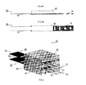
Figs. 3A-3B are views whereinFig. 3A is a lateral view showing an entire image of the millimeter wave sensor, andFig. 3B is a top view showing the millimeter wave sensor; and -
Fig. 4 is a perspective view of a millimeter wave imaging sensor showing a structure of the millimeter wave imaging sensor. - 1···millimeter wave imaging device, 10···lens antenna, 20···millimeter wave imaging sensor, 30···reflector, 32···reflection surface, 50···controller, 60···millimeter wave sensor, 62···antenna portion, 68···wave detection unit, 80···shielding member
- An embodiment of the present invention is described below with reference to the drawings.
As shown inFig. 1 , a millimeterwave imaging device 1 includes: alens antenna 10 that takes in millimeter waves emitted from a subject and forms an image of the subject; a millimeterwave imaging sensor 20 that takes an image of the subject by the millimeter waves emitted from the subject; areflector 30 having areflection surface 32 that reflects millimeter waves taken into thelens antenna 10 and guides the millimeter waves to the millimeterwave imaging sensor 20; and acontroller 50 that controls an entire operation of the millimeterwave imaging device 1. - In the millimeter
wave imaging sensor 20, a plurality ofmillimeter wave sensors 60 are disposed in a m×n matrix (m,n = 1,2, ···; but not m=1, n=1) on a plane that intersects an incoming direction of millimeter waves (a plane extending along the vertical direction inFig. 1 ). - As shown in
Fig. 2 , themillimeter wave sensors 60 are each equipped with: anantenna portion 62 extending toward the incoming direction of millimeter waves emitted from a subject; a low noise amplifier (LNA) 64 that amplifies received signals from theantenna portion 62; andwave detection unit 68 that detects signal levels of the received signals amplified by theLNA 64. These constituents, except for theantenna portion 62, are disposed on a plate-shaped substrate 70 extending along the incoming direction of millimeter waves. Theantenna portion 62 is attached on thesubstrate 70 only in the rear end side thereof. - As shown in
Figs. 3A and 3B , each of themillimeter wave sensors 60 is provided with aconductive shielding member 80 that surrounds an area on thesubstrate 70, which includes: a transmission path, extending from theantenna portion 62 to thewave detection unit 68; theLNA 64; and thewave detection unit 68. Theshielding member 80 is made of a conductive metal material. - The
shielding member 80 is formed in a manner so that the outer peripheral shape thereof contacting with adjacently disposed millimeter wave sensors 60 (to be referred to as "adjacent outer peripheral shape") contacts with theshielding members 80 of the adjacentmillimeter wave sensors 60 so as to set the mutual positions of the millimeter wave sensors 60 (seeFig. 4 ). - In the present embodiment, as the adjacent outer peripheral shape for disposing respective
millimeter wave sensors 60 in the m×n matrix, plane surfaces respectively parallel to the direction of the rows and the direction of the columns are adopted. Therefore, the cross sectional surfaces of the shieldingmembers 80, intersecting the incoming direction of millimeter waves, are formed in rectangular manners (the lower sides are open) surrounding the above-described areas. - From the respective
millimeter wave sensors 60 of the millimeterwave imaging sensor 20, detection values, corresponding to signal levels of millimeter waves received at respective reception points, are obtained. Thecontroller 50 sequentially takes in the detection values from the respectivemillimeter wave sensors 60 so as to generate image data. - In the millimeter
wave imaging sensor 20 constituted as above, theconductive shielding members 80, surrounding the areas on thesubstrates 70 including the transmission paths from theantenna portions 62 to thewave detection units 68,LNAs 64, and thewave detection units 68, can work as spacers that determine the positioning of the respective adjacentmillimeter wave sensors 60. - In this structure, the above-described transmission paths,
LNAs 64, and thewave detection units 68 are not disposed in the rear end sides of the millimeter wave sensors 60 (seeFigs. 3A and 3B ) due to a structural reason. In such structure wherein positioning is determined by the shieldingmembers 80 surrounding some areas including these constituents, the positioning can be done in the front end sides of themillimeter wave sensors 60, as compared to a structure wherein positioning is done by using the rear ends of millimeter wave sensors. - Consequently, the positioning becomes less affected by misalignment caused while the
millimeter wave sensors 60 are secured, or warpage of the members caused after the securing. As a result, themillimeter wave sensors 60 can be respectively secured with high positioning accuracy, and the high positioning accuracy can be easily maintained. - In the above-described structure, the shielding
members 80 are made of a conductive metal material. Therefore, heat dissipation effect, corresponding to heat-transfer coefficient of the material, can be expected.
The above explained an embodiment of the present invention. However, it is to be noted that the present invention is not limited to the above-described embodiment, and that variations can be adopted within the technical scope of the present invention. - For example, in the above-described embodiment, an example is illustrated wherein the
millimeter wave sensors 60 of the millimeterwave imaging sensor 20 are respectively disposed in such a manner so that the plurality ofmillimeter wave sensors 60 is placed in the m×n matrix on the plane intersecting the incoming direction of millimeter waves. Alternatively, the plurality ofmillimeter wave sensors 60 may be disposed other than in the m×n matrix. - Moreover, in the above-described embodiment, an example is illustrated wherein the adjacent peripheral shape for disposing the respective
millimeter wave sensors 60 of the millimeterwave imaging sensor 20 in the m×n matrix is planes respectively extending along the row direction and the column direction. However, the adjacent peripheral shape may be in any shape, other than the above-described shape, as long as the positioning of themillimeter wave sensors 60 can be mutually determined.
Claims (3)
- A millimeter wave imaging sensor comprising a plurality of millimeter wave sensors disposed on one plane intersecting an incoming direction of millimeter waves emitted from a subject, each of the plurality of millimeter wave sensors including:an antenna portion extending toward the incoming direction of the millimeter waves;a wave detection unit that detects signal levels of the millimeter waves received by the antenna portion;a transmission path that connects the antenna portion and the wave detection unit; anda shielding member that is conductive and surrounds the transmission path,wherein, among the plurality of millimeter wave sensors, adjacent millimeter wave sensors are positioned according to outer peripheral shape of the shielding members of the adjacent millimeter wave sensors.
- The millimeter wave imaging sensor according to claim 1,
wherein each of the plurality of millimeter wave sensors includes a plate-like substrate extending along the incoming direction of the millimeter waves,
wherein the transmission path and the wave detection unit are disposed on the substrate, and
wherein the shielding member surrounds an area on the substrate including at least an area where the transmission path is disposed. - The millimeter wave imaging sensor according to claim 1 or claim 2, wherein the shielding member is made of a conductive metal material.
Applications Claiming Priority (2)
| Application Number | Priority Date | Filing Date | Title |
|---|---|---|---|
| JP2009136440A JP5403670B2 (en) | 2009-06-05 | 2009-06-05 | Millimeter wave imaging sensor |
| PCT/JP2010/059566 WO2010140692A1 (en) | 2009-06-05 | 2010-06-04 | Millimeter wave imaging sensor |
Publications (2)
| Publication Number | Publication Date |
|---|---|
| EP2439554A1 true EP2439554A1 (en) | 2012-04-11 |
| EP2439554A4 EP2439554A4 (en) | 2012-11-14 |
Family
ID=43297824
Family Applications (1)
| Application Number | Title | Priority Date | Filing Date |
|---|---|---|---|
| EP10783474A Withdrawn EP2439554A4 (en) | 2009-06-05 | 2010-06-04 | MILLIMETER WAVE IMAGE SENSOR |
Country Status (6)
| Country | Link |
|---|---|
| US (1) | US20120168625A1 (en) |
| EP (1) | EP2439554A4 (en) |
| JP (1) | JP5403670B2 (en) |
| CN (1) | CN102460210A (en) |
| SG (1) | SG176257A1 (en) |
| WO (1) | WO2010140692A1 (en) |
Families Citing this family (2)
| Publication number | Priority date | Publication date | Assignee | Title |
|---|---|---|---|---|
| RU2516000C2 (en) * | 2012-04-19 | 2014-05-20 | Федеральное государственное военное образовательное учреждение высшего профессионального образования "Военный авиационный инженерный университет" (г. Воронеж) Министерства обороны Российской Федерации | Method of identifying and determining parameters of image of object on radar images |
| RU2561066C1 (en) * | 2014-04-24 | 2015-08-20 | Федеральное государственное унитарное предприятие "Ростовский-на-Дону научно-исследовательский институт радиосвязи" (ФГУП "РНИИРС") | Method of obtaining radio images of extended objects |
Family Cites Families (9)
| Publication number | Priority date | Publication date | Assignee | Title |
|---|---|---|---|---|
| US4910523A (en) * | 1987-11-06 | 1990-03-20 | Millitech Corporation | Micrometer wave imaging device |
| US6005531A (en) * | 1998-09-23 | 1999-12-21 | Northrop Grumman Corporation | Antenna assembly including dual channel microwave transmit/receive modules |
| JP2004120325A (en) * | 2002-09-26 | 2004-04-15 | Toshiba Corp | Antenna equipment |
| US7064328B2 (en) * | 2003-10-22 | 2006-06-20 | Northrop Grumman Corporation | Ultra sensitive silicon sensor millimeter wave passive imager |
| US7212153B2 (en) * | 2003-12-05 | 2007-05-01 | Safeview, Inc. | Millimeter-wave active imaging system with fixed array |
| US7119740B2 (en) * | 2003-12-05 | 2006-10-10 | Safeview, Inc. | Millimeter-wave active imaging system with modular array |
| EP1747602B1 (en) * | 2004-05-17 | 2009-03-04 | Sensis Corporation | A line-replaceable transmit/receive unit for multi-band active arrays |
| US7046209B1 (en) * | 2004-10-21 | 2006-05-16 | The Boeing Company | Design and fabrication methodology for a phased array antenna with shielded/integrated feed structure |
| CN101068054B (en) * | 2007-06-07 | 2011-06-08 | 京信通信系统(中国)有限公司 | Flat-plate antenna and packaging device and bushing device |
-
2009
- 2009-06-05 JP JP2009136440A patent/JP5403670B2/en not_active Expired - Fee Related
-
2010
- 2010-06-04 WO PCT/JP2010/059566 patent/WO2010140692A1/en not_active Ceased
- 2010-06-04 EP EP10783474A patent/EP2439554A4/en not_active Withdrawn
- 2010-06-04 CN CN2010800247216A patent/CN102460210A/en active Pending
- 2010-06-04 SG SG2011087608A patent/SG176257A1/en unknown
- 2010-06-04 US US13/376,292 patent/US20120168625A1/en not_active Abandoned
Also Published As
| Publication number | Publication date |
|---|---|
| EP2439554A4 (en) | 2012-11-14 |
| WO2010140692A1 (en) | 2010-12-09 |
| JP2010281738A (en) | 2010-12-16 |
| US20120168625A1 (en) | 2012-07-05 |
| CN102460210A (en) | 2012-05-16 |
| SG176257A1 (en) | 2012-01-30 |
| JP5403670B2 (en) | 2014-01-29 |
Similar Documents
| Publication | Publication Date | Title |
|---|---|---|
| US11703561B2 (en) | Radar device for vehicle | |
| EP4020714B1 (en) | Folded waveguide for antenna | |
| US11316280B2 (en) | Tiling system and method for an array antenna | |
| US8270157B2 (en) | Electronic device | |
| US20120306720A1 (en) | Antenna unit and panel array antenna device | |
| JP6214836B1 (en) | Light receiving unit and image sensor | |
| KR20110081990A (en) | Sensors, Systems, and Methods for Detecting Locations | |
| JP2007329714A (en) | Compound eye imaging device | |
| CN103179313A (en) | Image sensor unit, image reading apparatus, and image forming apparatus | |
| US20120168625A1 (en) | Millimeter Wave Imaging Sensor | |
| KR20160026571A (en) | Test socket for semiconductor devices and test equipment comprising the same | |
| US7512212B2 (en) | Multi-array detector module structure for radiation imaging | |
| JP2012047550A (en) | Radiation detector unit | |
| US9689973B2 (en) | Acoustic probe with components of acoustic elements having different pitches than each other | |
| US8766742B2 (en) | Integrated hybrid-direct couplers | |
| JP2007155563A (en) | Radiological image detection device | |
| US7696944B2 (en) | Antenna apparatus | |
| JP2016170048A (en) | Meteorological radar apparatus | |
| JP7541552B2 (en) | SENSOR SHIFT ACTUATOR DEVICE, IMAGING MODULE, AND ELECTRONIC DEVICE | |
| KR101369667B1 (en) | Holding structure of image pickup device and image pickup device | |
| KR102766405B1 (en) | X-ray detector | |
| CN111934096A (en) | K-band phased array element corner cutting array method | |
| JPWO2016158109A1 (en) | Imaging component and imaging module including the same | |
| EP4154038B1 (en) | Matrix of detectors with staggered columns | |
| US20230387577A1 (en) | Antenna structure and display device including the same |
Legal Events
| Date | Code | Title | Description |
|---|---|---|---|
| PUAI | Public reference made under article 153(3) epc to a published international application that has entered the european phase |
Free format text: ORIGINAL CODE: 0009012 |
|
| 17P | Request for examination filed |
Effective date: 20111229 |
|
| AK | Designated contracting states |
Kind code of ref document: A1 Designated state(s): AL AT BE BG CH CY CZ DE DK EE ES FI FR GB GR HR HU IE IS IT LI LT LU LV MC MK MT NL NO PL PT RO SE SI SK SM TR |
|
| DAX | Request for extension of the european patent (deleted) | ||
| A4 | Supplementary search report drawn up and despatched |
Effective date: 20121015 |
|
| RIC1 | Information provided on ipc code assigned before grant |
Ipc: G01S 7/03 20060101ALI20121009BHEP Ipc: H01P 1/00 20060101ALI20121009BHEP Ipc: G01S 13/89 20060101AFI20121009BHEP Ipc: H01Q 15/23 20060101ALI20121009BHEP Ipc: H01Q 19/06 20060101ALI20121009BHEP Ipc: H01Q 21/06 20060101ALI20121009BHEP |
|
| STAA | Information on the status of an ep patent application or granted ep patent |
Free format text: STATUS: THE APPLICATION IS DEEMED TO BE WITHDRAWN |
|
| 18D | Application deemed to be withdrawn |
Effective date: 20130514 |