EP2439172A1 - Anti-stiction method in an inertial MEMS - Google Patents
Anti-stiction method in an inertial MEMS Download PDFInfo
- Publication number
- EP2439172A1 EP2439172A1 EP10186715A EP10186715A EP2439172A1 EP 2439172 A1 EP2439172 A1 EP 2439172A1 EP 10186715 A EP10186715 A EP 10186715A EP 10186715 A EP10186715 A EP 10186715A EP 2439172 A1 EP2439172 A1 EP 2439172A1
- Authority
- EP
- European Patent Office
- Prior art keywords
- stiction
- electrodes
- pair
- mobile
- fingers
- Prior art date
- Legal status (The legal status is an assumption and is not a legal conclusion. Google has not performed a legal analysis and makes no representation as to the accuracy of the status listed.)
- Granted
Links
- 238000000034 method Methods 0.000 title claims abstract description 54
- 238000006073 displacement reaction Methods 0.000 claims description 16
- 230000004044 response Effects 0.000 claims description 5
- 230000001133 acceleration Effects 0.000 claims description 4
- 238000004590 computer program Methods 0.000 claims description 4
- 230000008569 process Effects 0.000 description 17
- 238000000926 separation method Methods 0.000 description 14
- 230000000694 effects Effects 0.000 description 8
- 230000006870 function Effects 0.000 description 6
- 238000000576 coating method Methods 0.000 description 5
- 239000011248 coating agent Substances 0.000 description 4
- 238000001514 detection method Methods 0.000 description 3
- 239000006185 dispersion Substances 0.000 description 3
- 239000000463 material Substances 0.000 description 3
- 238000004519 manufacturing process Methods 0.000 description 2
- 230000007246 mechanism Effects 0.000 description 2
- 230000000630 rising effect Effects 0.000 description 2
- 238000004381 surface treatment Methods 0.000 description 2
- 238000004873 anchoring Methods 0.000 description 1
- 238000010420 art technique Methods 0.000 description 1
- 230000008859 change Effects 0.000 description 1
- 238000005259 measurement Methods 0.000 description 1
- 238000004377 microelectronic Methods 0.000 description 1
- 239000004065 semiconductor Substances 0.000 description 1
- 230000035945 sensitivity Effects 0.000 description 1
- 230000035939 shock Effects 0.000 description 1
- 229910052710 silicon Inorganic materials 0.000 description 1
- 239000010703 silicon Substances 0.000 description 1
- 239000000126 substance Substances 0.000 description 1
- 239000000758 substrate Substances 0.000 description 1
- 238000012876 topography Methods 0.000 description 1
Images


Classifications
-
- G—PHYSICS
- G01—MEASURING; TESTING
- G01P—MEASURING LINEAR OR ANGULAR SPEED, ACCELERATION, DECELERATION, OR SHOCK; INDICATING PRESENCE, ABSENCE, OR DIRECTION, OF MOVEMENT
- G01P21/00—Testing or calibrating of apparatus or devices covered by the preceding groups
-
- B—PERFORMING OPERATIONS; TRANSPORTING
- B81—MICROSTRUCTURAL TECHNOLOGY
- B81C—PROCESSES OR APPARATUS SPECIALLY ADAPTED FOR THE MANUFACTURE OR TREATMENT OF MICROSTRUCTURAL DEVICES OR SYSTEMS
- B81C1/00—Manufacture or treatment of devices or systems in or on a substrate
- B81C1/00912—Treatments or methods for avoiding stiction of flexible or moving parts of MEMS
- B81C1/0096—For avoiding stiction when the device is in use, i.e. after manufacture has been completed
- B81C1/00968—Methods for breaking the stiction bond
-
- B—PERFORMING OPERATIONS; TRANSPORTING
- B81—MICROSTRUCTURAL TECHNOLOGY
- B81B—MICROSTRUCTURAL DEVICES OR SYSTEMS, e.g. MICROMECHANICAL DEVICES
- B81B3/00—Devices comprising flexible or deformable elements, e.g. comprising elastic tongues or membranes
- B81B3/0018—Structures acting upon the moving or flexible element for transforming energy into mechanical movement or vice versa, i.e. actuators, sensors, generators
-
- G—PHYSICS
- G01—MEASURING; TESTING
- G01P—MEASURING LINEAR OR ANGULAR SPEED, ACCELERATION, DECELERATION, OR SHOCK; INDICATING PRESENCE, ABSENCE, OR DIRECTION, OF MOVEMENT
- G01P15/00—Measuring acceleration; Measuring deceleration; Measuring shock, i.e. sudden change of acceleration
- G01P15/02—Measuring acceleration; Measuring deceleration; Measuring shock, i.e. sudden change of acceleration by making use of inertia forces using solid seismic masses
- G01P15/08—Measuring acceleration; Measuring deceleration; Measuring shock, i.e. sudden change of acceleration by making use of inertia forces using solid seismic masses with conversion into electric or magnetic values
- G01P15/125—Measuring acceleration; Measuring deceleration; Measuring shock, i.e. sudden change of acceleration by making use of inertia forces using solid seismic masses with conversion into electric or magnetic values by capacitive pick-up
-
- B—PERFORMING OPERATIONS; TRANSPORTING
- B81—MICROSTRUCTURAL TECHNOLOGY
- B81B—MICROSTRUCTURAL DEVICES OR SYSTEMS, e.g. MICROMECHANICAL DEVICES
- B81B2201/00—Specific applications of microelectromechanical systems
- B81B2201/02—Sensors
- B81B2201/0228—Inertial sensors
- B81B2201/0235—Accelerometers
Abstract
- a mobile mass (150), suspended to an armature via spring means (115), comprising at least one mobile electrode; and
- at least one fixed electrode rigidly attached to the armature, each fixed electrode cooperating with one of said at least one mobile electrode to form a pair of electrodes.
Description
- The field of the invention is that of inertial micro-electro-mechanical systems (also called inertial MEMS), used as inertial sensors, such as accelerometers or gyroscopes for example.
- More specifically, the invention pertains to a technique for overcoming stiction of micro-surfaces facing one another, such as conductive electrodes in an inertial MEMS device.
- The invention can apply specially but not exclusively in the implementation of an inertial MEMS device comprising conductive electrodes that are equipped with conductive fingers.
- MEMS are very small integrated systems that combine mechanical and electrical components, which traditionally range in size from the micrometer to the millimeter level.
- The difficulty in controlling surface forces existing inside inertial MEMS devices is a critical obstacle to their fabrication and using. In particular, surface phenomena such as stiction of two micro-surfaces facing one another frequently restrict the operational environment and limit the lifetime of these devices.
- By definition, stiction phenomenon occurs when surface adhesion forces (or stiction forces) are higher than mechanical restoring forces of the micro-surfaces.
- In addition, with the decrease in the dimension of MEMS microstructures over recent years, this surface phenomenon has become more and more effective.
- A well-known problem is in-use stiction that appears during operation and handling of inertial MEMS devices when micro-surfaces, such as conductive electrodes, come into contact and permanently adhere to each other, causing MEMS failure. In-use stiction may be caused by the following stiction forces: capillary, electrostatic (or Van Der Walls) and chemical bonding forces. Those stiction forces essentially depend upon nature of the used materials in the inertial MEMS device, surface topography and surface treatment method.
- One particular structure of such an inertial MEMS device, as illustrated in
figure 1 , consists for example of amobile mass 150 comprising one mobile electrode, suspended by springs means 115 to an armature (not shown), said mobile electrode comprising a plurality ofconductive fingers 155. The inertial MEMS device further comprises two sets of twofixed electrodes conductive fingers conductive finger mobile mass fingers 155 to form a pair of conductive fingers (with associated capacitance value) that is used to move down or up the mobile mass along asensitive axis 130. - Here below, "spring means" (also called "flexible beam") is understood to be every flexible connection means for elastically relying the mobile mass to the armature.
- The technical problem of reducing probability of finger stiction in-use of an inertial MEMS device is a problem known by a person skilled in the art and several techniques have been provided to solve it.
- A first known technique consists in rising restoring forces of
springs 115 by rising spring stiffness and/or mobile mass excursion. But to obtain higher spring stiffness, inertial MEMS developers are forced to conceive more massive springs, which makes the inertial MEMS device less compact. Also, if spring stiffness increases, sensitivity of the inertial MEMS device and so signal-to-noise ratio (or SNR) are reduced. - Furthermore, even for an inertial MEMS device comprising such massive springs, in-use stiction phenomenon still persists.
- A second known technique consists in reducing stiction forces by means of a suitable coating of surfaces of the conductive fingers which are susceptible to come in contact, such a coating - as known as "anti-stiction coating" - being made of a low-energy surface material and/or a high-roughness surface material.
- However, low-energy surface coatings require a surface treatment process, which has the well-known drawbacks of complexity of implementation, manufacture and of cost.
- In addition, even for conductive finger surfaces treated with an anti-stiction coating, in-use stiction phenomenon is still of concern.
- Therefore, one common drawback of these two aforesaid prior-art techniques is that they are not sufficiently effective, since they do not ensure that the problem of MEMS in-use stiction is totally eliminated. It therefore becomes impossible to ensure to a user that his inertial MEMS device will not be in a non-functioning state.
- To overcome this drawback, it may be a common practice to apply one or several mechanical shock(s) to the MEMS device according to its sensitive axis, for example by means of a vibration system, in order to add an additional force component to the restoring force of springs so as to generate a restoring force higher than the stiction forces. This practice can be complex to implement and cost a lot.
- The invention, in at least one embodiment, is aimed especially at overcoming this drawback of the prior art.
- More specifically, it is a goal of at least one embodiment of the invention to provide an anti-stiction technique that overcomes the undesirable effects related to the stiction of conductive fingers (or more generally of conductive electrodes) within an inertial MEMS device.
- At least one embodiment of the invention is also aimed at providing a technique of this kind that is simple to implement and costs little.
- It is another goal of at least one embodiment of the invention to provide a technique that relies solely on means classically used within an inertial MEMS device.
- One particular embodiment of the invention proposes an anti-stiction method in an inertial micro-electro-mechanical device comprising:
- a mobile mass, suspended to an armature via spring means, said mobile mass comprising at least one mobile electrode; and
- at least one fixed electrode rigidly attached to said armature, each fixed electrode cooperating with one of said at least one mobile electrode to form a pair of electrodes;
- a step of detecting, for at least one stuck pair of electrodes, a stiction associated to a stiction force;
- at least one separating step, comprising a step of applying, during a predetermined time period, a predetermined voltage between the electrodes of at least one of said pair or pairs of electrodes, to create an electrostatic force.
- The general principle of one particular embodiment of the invention therefore is that of, upon detection of presence of a stiction of one pair or several pairs of electrodes used to move the mobile mass within a MEMS device, carrying out a mechanism for separating the electrodes of this pair or those pairs of electrodes for which a stiction has been detected. Such a separating mechanism consists in displacing, by simple application of a predetermined voltage between the electrodes of at least one of said pair or said pairs of electrodes, the mobile mass according to the sensitive axis of the MEMS device, in order to attempt to overcome the electrode stiction.
- Thus, only a simple voltage application being necessary to overcome the electrode stiction, this embodiment of the invention provides an anti-stiction method that relies solely on means classically used in inertial MEMS devices and so that is simple to implement and costs little.
- Advantageously, each pair of electrodes forms a variable capacitance, and said step of detecting the stiction consists in measuring a differential capacitance between:
- a first capacitance of at least one pair of electrodes enabling a displacement of the mobile mass according to a first direction; and
- a second capacitance of at least one pair of electrodes enabling a displacement of the mobile mass according to a second direction opposite to said first direction.
- By means of a simple measurement of a differential capacitance, it is thus possible to detect an electrode stiction, the sign of this differential capacitance enabling to know the direction in which the stiction occurs. Therefore, an appropriate anti-stiction process may be carrying out as a function of the known stiction direction.
- According to an advantageous feature, said predetermined voltage is applied between the electrodes of at least one of said pair or pairs of electrodes, distinct from said at least one stuck pair of electrodes, so as to create an electrostatic force according to a direction opposite to the direction of said stiction force.
- The fact of applying a predetermined voltage so that the mobile mass moves according to a direction opposite to the stiction force direction (called hereafter "first separating step"), enables to constrain the electrodes of the pair or pairs of electrodes for which a stiction has been detected to separate from each other. Indeed, according to this advantageous feature, causing a movement of the mass mobile to a direction opposed to the stiction force direction enables to add an additional force to the restoring force of springs, thereby improving the probability for unsticking the electrodes of stuck pair or pairs of electrodes.
- According to a variant, said predetermined voltage is applied between the electrodes of at least one pair or pairs of electrodes, so as to create an electrostatic force which generates a displacement of the mobile mass according to the direction of said stiction force.
- In that way, said displacement of the mobile mass deforms said spring means and said at least one stuck pair of electrodes, thereby generating first and second restoring forces respectively, so that after said predetermined time period has elapsed, said first and second restoring forces are applied to said at least one stuck pair of electrodes.
- Thus, the fact of applying a predetermined voltage so as to generate a movement of the mobile mass according to the direction of the stiction force (called hereafter "second separating step"), then canceling the predetermined voltage, enables to create a "bow effect", the restoring forces of which being such that they efficiently displace the mass mobile in a direction opposite to the stiction force direction. Such a bow effect therefore enables to improve the probability for unsticking the electrodes of stuck pair or pairs of electrodes.
- According to a preferential feature, for at least one of said pairs of electrodes, the device comprises at least one contact stop attached to one electrode of said at least one pair of electrodes, and extending towards the other electrode of at least one pair of electrodes to limit contact surface of the electrodes.
- Electrodes of a stuck pair of electrodes endowed with a contact stop having a low-energy surface, the unsticking probability of these electrodes is thus improved.
- In a hypothetical case in which all pairs of electrodes between which the predetermined voltage is applied are stuck, the presence of one or more contact stops on the fixed electrode and/or mobile electrode nevertheless gives the possibility to create an electrostatic force that generates a displacement of the mobile mass according to the direction of said stiction force in order to separate electrodes of all or part of stuck pairs of electrodes. Indeed, a contact stop has a very low level of conductivity, which avoids having a total short-circuit of a pair of electrodes when these electrodes are stuck. Furthermore, there is a size dispersion of the contact stops, giving impossibility of having the same size of contact stop on the set of pairs of electrodes of the MEMS device
- Therefore, even if this hypothetical case occurs, it is possible to generate an effective bow effect.
- Advantageously, when said predetermined time period has elapsed, said predetermined voltage is stopped within a time-stop period such that the ratio between the time-stop period and the response of the mass-spring system formed by said mobile mass and said spring means, is inferior or equal to 10%.
- Thus, an effective "bow effect" is ensured to be performed.
- Preferably, the aforesaid first separating step is preceded or followed by the aforesaid second separating step.
- In that way, if the first separating step does not enable to overcome the electrode stiction which has been detected, it is thus possible to carry out the second separating step (and inversely), in order to ensure a definite separation of the electrodes.
- In case the separation of the electrodes of stuck pair or pairs of electrodes has not been obtained after executing the first and second separation steps, it may eventually be an advantageous practice to reiterate as many times as necessary the first and/or second separation steps one after the other until a separation of the electrodes is definitively obtained.
- Preferentially, said at least one mobile electrode comprises a plurality of mobile fingers and said at least one fixed electrodes comprises a plurality of fixed fingers, each fixed finger cooperating with one mobile finger to form a pair of fingers forming a capacitance, each mobile finger being movable relative to one fixed finger under an acceleration, thus creating a variation of capacitance, and said predetermined voltage is applied between the fingers of at least one of said pair or pairs of fingers, so as to create said electrostatic force.
- Advantageously, for at least one of said pairs of fingers, the device comprises at least one contact stop attached to one finger of said at least one pair of fingers, and extending towards the other finger of at least one pair of fingers to limit contact surface of the fingers. Besides the fact of having fingers with a low-energy surface, the bow effect is optimized thanks to the presence of such contact stop.
- In practice, they are the fingers of unstuck pairs of fingers that enable to create a bow effect. In a hypothetical case in which all pairs of fingers are stuck, the presence of contact stops on the fixed finger and/or mobile finger nevertheless gives the possibility to create an electrostatic force that generates a displacement of the mobile mass according to the direction of said stiction force, thereby causing separation of fingers of all or part of stuck pairs of fingers. Indeed, in the one hand, a contact stop has a very low level of conductivity, which avoids having a total short-circuit of a pair of fingers when these fingers are stuck. In the other hand, there is a size dispersion of the contact stops, giving impossibility of having the same size of contact stop on the set of pairs of fingers of the MEMS device. The same reasoning may be also applied on the dispersion of distance between the mobile and fixed fingers of the set of the pairs of fingers of the MEMS device. Thus, the probability of having all pairs of fingers stuck is extremely weak.
- In another embodiment of the invention, there is proposed a computer program product comprising program code instructions for implementing the above-mentioned method (in any one of its different embodiments) when said program is executed on a computer.
- In another embodiment of the invention, there is proposed a computer-readable storage means storing a computer program comprising a set of instructions executable by a computer to implement the above-mentioned method (in any one of its different embodiments).
- In another embodiment of the invention, there is proposed an anti-stiction device intended to cooperate with an inertial micro-electro-mechanical device comprising:
- a mobile mass, suspended to an armature via spring means, said mobile mass comprising at least one mobile electrode; and
- at least one fixed electrode rigidly attached to said armature, each fixed electrode cooperating with one of said at least one mobile electrode to form a pair of electrodes;
- means for detecting, for at least one stuck pair of electrodes, a stiction associated to a stiction force;
- means for separating said at least one stuck pair of electrodes, by applying, during a predetermined time period, a predetermined voltage between the electrodes of at least one of said pair or pairs of electrodes, to create an electrostatic force.
- Other features and advantages of embodiments of the invention shall appear from the following description, given by way of an indicative and non-exhaustive example, and from the appended drawings, of which:
-
Figure 1 already described with reference to the prior art, presents a schematic example of the structure of an inertial MEMS device on which the anti-stiction method can be implemented; -
Figure 2 illustrates a first example of an anti-stiction process applied to the inertial MEMS device offigure 1 , according to a particular embodiment of the invention; -
Figures 3a and 3b illustrate a second example of an anti-stiction process applied to the inertial MEMS device offigure 1 , according to another particular embodiment of the invention,figure 3a and 3b illustrating a first phase and a second phase of this anti-stiction process respectively; -
Figure 4 shows the schematic structure of an anti-stiction device implementing the anti-stiction method, according to one particular embodiment of the invention; -
Figure 5 represents a graph illustrating evolution of the electrostatic force, necessary to obtain a stuck-finger separation as a function of the distance between fingers, according to one particular embodiment of the invention. - In all the figures of the present document, the identical elements and steps are designated by a same numerical reference.
-
Figures 1 ,2 ,3a and 3b described below concern a schematic example of the structure of an inertial MEMS device on which is implemented the anti-stiction method, according to a particular embodiment of the invention. Such a device comprising one mobile mass suspended to an armature via spring means and equipped with one mobile electrode, and several fixed electrodes. More precisely, the mobile electrode comprises a plurality of mobile conductive fingers and each fixed electrode comprises a plurality of fixed conductive fingers, each fixed finger being placed in front and parallel of (and cooperating with) one corresponding mobile finger to form a pair of conductive fingers. It is understood that the inertial MEMS device to which the present invention can be applied may have conductive electrodes with no fingers and the illustratory example described in detail here below would be adapted accordingly. Especially, the anti-stiction method illustrated below is applied to separate conductive fingers (thereby considered as conductive electrodes) but can more generally be applied to separate conductive electrodes that are not equipped with conductive fingers. -
Figure 1 already described with reference to the prior art, shows a schematic example of the structure of aninertial MEMS device 100 on which the anti-stiction method can be implemented, according to a particular embodiment of the invention.. Theinertial MEMS device 100 comprises the following elements: - an armature (not shown in
figure 1 ) to which are attached fixedsupports 110 and anchoring means 140; - a
mobile mass 150, forming a mobile electrode which is suspended from the fixedsupports 110, bysprings 115 and endowed with severalconductive fingers 155; - a first set of two fixed
electrodes 120a, rigidly attached to the armature, each comprising twoconductive fingers 125a, each cooperating with one of the mobilemass fingers 155 to form a pair of fingers (125a,155) used to move down themobile mass 150 along thesensitive axis 130; - a second set of two fixed
electrodes 120b, rigidly attached to the armature, each comprising twoconductive fingers 125b, each cooperating with one of the mobilemass fingers 155 to form a pair of fingers (125b,155) used to move up themobile mass 150 along thesensitive axis 130. - The mobile mass 150 - i.e. the mobile electrode - (and its fingers), the armature, the two sets of fixed electrodes (and their fingers) and the springs are micromachined in a semi-conductor substrate (Silicon for example), by means of usual microfabrication technological processes of microelectronics.
- The mobile electrode is electrically insulated from the fixed electrodes. Each pair of fingers of the
MEMS device 100 constitutes a variable capacitance for measuring the displacements of themobile mass 150 and controlling the displacements thereof according to thesensitive axis 130 by means of application of a predetermined voltage. - The fixed and mobile electrodes thus fulfill, via the pairs of fingers two functions:
- detecting the position of the
mobile mass 150 relative to the armature by measuring variation of the capacitance of pairs of fingers; - generating electrostatic forces, which make the
mobile mass 150 moving up or down along thesensitive axis 130 as a function of the set of fixedelectrodes MEMS device 100 may be associated with an electronic feedback system (non illustrated onfigure 1 ), which enables to replace the mobile mass in an idle position after having detected a displacement of the mobile mass. In way of example, the displacement of the mobile mass is due to a seismic acceleration applied to the MEMS device, such as an accelerometer. Feedback electrostatic forces applied to the mobile mass by means of a voltage generated between the fixed and mobile electrodes compensate for the seismic acceleration in view to place again the mobile mass in an idle position. - In a particular embodiment of the invention, each fixed
electrode finger stop - It should be noted that the number of fixed electrodes and of fingers shown in
figure 1 (as well asfigures 2 ,3a and 3b ) is deliberately limited by way of a purely pedagogical description, so as not to burden the figure and the associated description. -
Figure 2 illustrates a first example of an anti-stiction process applied to the inertial MEMS device offigure 1 , according to one particular embodiment of the invention. - Contrary to the example of
figure 1 according to which the mobile mass is in an idle position (sincesprings 115 are not deformed), the mobile mass infigure 2 is in a contact position (since springs are deformed). The spring deformation is due to presence of a finger stiction of the pair offingers 200 located in top left of the MEMS device. - As a general principle, the step of detecting the stiction consists in measuring the differential capacitance (noted ΔC below). As shown at the left of the
sensitive axis 130 offigure 1 , two variable capacitances are defined: - a first variable capacitance C1 which represents the average capacitance of all the pairs of fingers (125a, 155) used to move down the
mobile mass 150 along thesensitive axis 130; and - a second variable capacitance C2 which represents the average capacitance of all the pairs of fingers (125b, 155) used to move up the
mobile mass 150 along thesensitive axis 130. - In case of stiction (for example stiction of fingers of the pair of fingers referenced 200 on
figure 2 ), themobile mass 150 is far from its idle position and a differential capacitance between the first and second variable capacitances, defined as ΔC = C1-C2, can be detected and measured by electronics means. As it is possible to determine the sign of this differential capacitance ΔC, it is further possible to know the direction in which the stiction occurs (up or down along the sensitive axis 130) and therefore carry out the anti-stiction process as a function of the known stiction direction. - It should be noted that, when a stiction occurs, the mobile mass is in a contact position regardless of the fact that the MEMS device is in an idle state or in an active state.
- The finger stiction is defined by a stiction force (noted Fs), oriented downward according to an axis parallel to the sensitive axis 130a, which tends to sustain the
mobile mass 150 in a downward position. The resulting deformation of the foursprings 115 generates a restoring force (Fr), oriented according to a direction opposite to the stiction force direction. Generally, this restoring force is greater than the stiction force and in this case themobile mass 150 returns to the idle position. Here, as the restoring force is not greater than the stiction force, themobile mass 150 stays in a contact position (there is a stiction), and this could cause MEMS failure. In that first example, the anti-stiction process aims at applying a predetermined voltage, such as 30V for example, between each of the second set of fixedelectrodes 120b and the mobile electrode in order to generate an electrostatic force (noted Fe for the whole MEMS, and Fe/n for each pair of fingers) in the direction opposite to the finger stiction direction. The generated electrostatic force (Fe) acts as an additional force component (which is also opposite to the stiction force direction), so that the summation of the restoring force (Fr) exerted by thesprings 115 and the generated electrostatic force (Fe) tends to be upper than the stiction force Fs and cause a separation of fingers, which are responsible for the stiction. -
Figures 3a and 3b illustrate a second example of an anti-stiction process applied to the inertial MEMS device offigure 1 , according to a particular embodiment of the invention.Figure 3a and 3b illustrate a first phase and a second phase of this anti-stiction process respectively. - This particular embodiment of the invention consists in implementing a finger separating process based on a "bow effect". It is divided into two main phases detailed below.
- Here below, the finger stiction is considered to be located on top left of the MEMS device of
figure 1 . - After detecting presence of finger stiction for the upper fixed
electrode 120a, a first phase (figure 3a ) is executed. It consists in applying, during a short time period (such as 100µs for example) a predetermined voltage (a value comprised between 5 and 10V for example) so as to generate an electrostatic force (noted Fe) in the same direction as the one of the stiction force (noted Fs). This generated electrostatic force (Fe) creates a displacement of themobile mass 150 according to the stiction force direction, which deforms thesprings 115 and mainly the fixed electrode finger and the mobile electrode finger of the pair of fingers for which a stiction has been detected, such that:
with: - Fr, the spring restoring force due to the deformation of the four
springs 115; and - Ff, the finger restoring force due to both the deformation of the fixed
electrode finger 125a and themobile electrode finger 155. - Thus, the difference between Fe and Fr applies to the fixed electrode finger and the mobile electrode finger deformations.
- Each pair of
fingers 
with: - Kd : the spring stiffness of the pair of fingers:
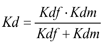
- Kdf : stiffness of the fixed electrode finger;
- Kdm : stiffness of the mobile electrode finger;
- Δxm : displacement of the
mobile mass 150, related to the deformation of the pair of fingers. A second phase (figure 3b ) is then executed. It consists in, after the short time period (of 100µs in this example) has elapsed, stopping applying the predetermined voltage between the first set of fixedelectrodes 120a and the mobile electrode. In that way, when the voltage is no longer generated (i.e. when the force Fe is no longer applied), the spring restoring force and the restoring force are applied to the mobile mass. - It must be noted that the voltage has to be stopped with a time-stop period such that the ratio between the time-stop period and the response time of the mass-spring system is inferior or equal to 10%. More precisely, by way of example, typical value for the time-stop period and the response of the mass-spring system are respectively 100 µs and 1ms.
- As a consequence, when the voltage is canceled, the deformation energy Edd of the pair of fingers changes into kinetic energy by transmitting velocity to the
mobile mass 150 in the form of axial thrust. - When the value of this deformation energy Edd is zero, the kinetic energy is maximal and the different forces, which are applied on the
mobile mass 150, are the spring restoring force Fr and the stiction force Fs. - In presence of a stiction force Fs, the
mobile mass 150 deforms the pair of fingers with a maximum use of kinetic energy and spring restoring force. When the kinetic energy disappears (i.e. when the pair of fingers (125a, 155) has a deformation opposite to the deformation in first phase), the finger restoring force Ff applies to the pair of fingers. Therefore, the maximum force (also called below as separating force) which applies on the pair of fingers, in order to cause a separation between the mobilemass finger 155 and the fixedelectrode finger 125a, is equal to the summation of the spring restoring force Fr and the finger restoring force Ff. In other words, this maximum force corresponds to the electrostatic force (Fe) that has been applied in phase 1. - To facilitate understanding of the phenomenon created during execution of the first and second phases, this one can be compared to the bandage of a bow which enables to store energy, this energy being then transmitted to the arrow when bandage is canceled.
- Now referring to
figure 4 , we present the simplified structure of ananti-stiction device 400 implementing the anti-stiction method, according to one particular embodiment of the invention. - The anti-stiction device includes:
- a read-only memory (ROM) 430;
- a random access memory (RAM) 410; and
- a
processor 420. - The read-
only memory 430 stores a executable code of the programs, which, when are executed by theprocessor 420, enable implementation of the technique of the invention, e.g., the rules and operations of which are described above in connection withfigures 2 ,3a and 3b . - Upon initialization, the aforementioned program code instructions are transferred to the
random access memory 410 so as to be executed by theprocessor 420. Therandom access memory 410 likewise includes registers for storing the variables and parameters required for this execution. Theprocessor 420 receives a stiction information indicating presence of stiction in the inertial MEMS device to which thestiction device 400 is associated and, according to the instructions of the aforementioned programs, delivers a voltage information indicating application of a predetermined voltage to the fixed electrodes. - All the steps of the anti-stiction process of
figures 2 ,3a, 3b can be implemented equally well: - by the execution of a set of computer instructions executed by a reprogrammable computing machine such as a PC type apparatus, a DSP (a digital signal processor) or a microcontroller can be stored in a storage medium that is detachable (for example a floppy disk, a CD-ROM or a DVD-ROM) or non-detachable; or else
- by a dedicated machine or component such as an FPGA (Field Programmable Gate Array), an ASIC (Application-Specific Integrated Circuit) or any dedicated hardware component.
-
Figure 5 represents a graph illustrating evolution of the electrostatic force Fe (µN), necessary to obtain a finger separation when the mobile mass is in contact position, as a function of the distance (µm) between fingers, according to one particular embodiment of the invention. - This graph shows:
- a
curve 501 that represents a first separating step and illustrates in particular evolution of the anti-stiction force (Fe+Fr) generated when the anti-stiction process offigure 2 is carried out; - a
curve 502 that represents a second separating step and illustrates in particular evolution of the anti-stiction force (Fe) generated when the anti-stiction process offigures 3a and 3b is carried out. - The distance d (µm) represents the average distance (or gap) separating fingers of each pair of fingers (125a,155), when at least one mobile mass finger (155) is in contact with one corresponding fixed electrode finger (125a) of a pair of fingers.
- As described above, the anti-stiction method implements the anti-stiction process of
figure 2 or the anti-stiction offigures 3a and 3b independently one of the other, according to one embodiment of the invention. - According to an embodiment variant, the anti-stiction method can implement a combination of the two anti-stiction processes described above in connection with
figures 2 ,3a and 3b . - For simplification reasons, we consider the description here below concerns the
inertial MEMS device 100 offigure 1 . - Upon detection of a stiction, the first separating step (curve 501) is executed by generating a voltage of value V1 between the mobile electrode and the set of fixed electrodes for which at least one stiction has been detected, in order to create a displacement of the mobile mass in the same direction as the one of the stiction force.
- If no separation of fingers has occurred by this first anti-stiction step, i.e. upon detection of a stiction, the second separating step (curve 502) is then executed. This second step consists in applying, during a predetermined period of time, a voltage of value V2 between the mobile electrode and the set of fixed electrodes for which no stiction has been detected, then, when the predetermined period of time has elapsed, stopping applying the voltage V2 with a given time-stop period (corresponding for example to a value comprised between 1/10 and 1/4 of the response time of the mass-spring system), in order to create an electrostatic force in the direction opposite to the direction of the stiction force.
- In that way, if the first separating step does not enable to overcome the fingers stiction, it is thus possible to carry out the second separating step, in order to ensure a definite separation of the fingers.
- In case the finger separation has not been obtained after a first execution of this two separating steps, each or only one of these steps can be reiterated as many times as necessary one after the other until a separation of the fingers is definitively obtained.
- Thus, in accordance with the graph, applying successively the two separating steps enables to generate of a resulting separating force of at least 140µN, whatever the distance of fingers between them, which is upper than the stiction force.
- It must be noted that it is also possible to carry out the first and second separating steps without a detecting step of stiction is executed between this two separating steps.
- It must also be noted that it is possible to change the order of execution of the first and second separating steps (i.e. carrying out the second separating step, and then the first separating step, if necessary).
Claims (12)
- Anti-stiction method in an inertial micro-electro-mechanical device comprising:- a mobile mass (150), suspended to an armature via spring means (115), said mobile mass comprising at least one mobile electrode; and- at least one fixed electrode rigidly attached to said armature, each fixed electrode cooperating with one of said at least one mobile electrode to form a pair of electrodes;the method being characterized in that it comprises:- a step of detecting, for at least one stuck pair of electrodes, a stiction associated to a stiction force (Fs);- at least one separating step, comprising a step of applying, during a predetermined time period, a predetermined voltage between the electrodes of at least one of said pair or pairs of electrodes, to create an electrostatic force.
- Anti-stiction method according to claim 1, characterized in that each pair of electrodes forms a variable capacitance, and in that said step of detecting the stiction consists in measuring a differential capacitance between:- a first capacitance of at least one pair of electrodes enabling a displacement of the mobile mass according to a first direction; and- a second capacitance of at least one pair of electrodes enabling a displacement of the mobile mass according to a second direction opposite to said first direction.
- Anti-stiction method according to any one of claims 1 to 2, characterized in that said predetermined voltage is applied between the electrodes of at least one of said pair or pairs of electrodes, distinct from said at least one stuck pair of electrodes, so as to create an electrostatic force according to a direction opposite to the direction of said stiction force.
- Anti-stiction method according to any one of claims 1 to 2, characterized in that said predetermined voltage is applied between the electrodes of at least one pair or pairs of electrodes, so as to create an electrostatic force which generates a displacement of the mobile mass according to the direction of said stiction force.
- Anti-stiction method according to any one of claims 3 and 4, characterized in that, for at least one of said pairs of electrodes, the device comprises at least one contact stop attached to one electrode of said at least one pair of electrodes, and extending towards the other electrode of at least one pair of electrodes to limit contact surface of the electrodes.
- Anti-stiction method according to any one of claims 1 to 5, characterized in that, when said predetermined time period has elapsed, said predetermined voltage is stopped within a time-stop period such that the ratio between the time-stop period and the response of the mass-spring system formed by said mobile mass (150) and said spring means (115), is inferior or equal to 10%.
- Anti-stiction method according to claim 1, characterized in that it comprises a first separating step according to claim 3, being preceded or followed by a second separating step according to claim 4 or 5.
- Anti-stiction method according to any one of claims 1 to 7, characterized in that said at least one mobile electrode comprises a plurality of mobile fingers (155) and said at least one fixed electrodes (120a, 120b) comprises a plurality of fixed fingers (125a, 125b), each fixed finger cooperating with one mobile finger to form a pair of fingers forming a capacitance, each mobile finger being movable relative to one fixed finger under an acceleration, thus creating a variation of capacitance,
and in that said predetermined voltage is applied between the fingers of at least one of said pair or pairs of fingers, so as to create said electrostatic force. - Anti-stiction method according to claim 8, characterized in that, for at least one of said pairs of fingers, the device comprises at least one contact stop attached to one finger of said at least one pair of fingers, and extending towards the other finger of at least one pair of fingers to limit contact surface of the fingers.
- Computer program product characterized in that it comprises program code instructions for implementing the method according to at least one of the claims 1 to 9, when said program is executed on a computer.
- Computer-readable storage means storing a computer program comprising a set of instructions executable by a computer to implement the method according to at least one of the claims 1 to 9.
- Anti-stiction device intended to cooperate with an inertial micro-electro-mechanical device comprising:- a mobile mass (150), suspended to an armature via spring means (115), said mobile mass comprising at least one mobile electrode; and- at least one fixed electrode rigidly attached to said armature, each fixed electrode cooperating with one of said at least one mobile electrode to form a pair of electrodes;the anti-stiction device being characterized in that it comprises:- means for detecting, for at least one stuck pair of electrodes, a stiction associated to a stiction force (Fs);- means for separating said at least one stuck pair of electrodes, by applying, during a predetermined time period, a predetermined voltage between the electrodes of at least one of said pair or pairs of electrodes, to create an electrostatic force.
Priority Applications (6)
| Application Number | Priority Date | Filing Date | Title |
|---|---|---|---|
| EP10186715.8A EP2439172B1 (en) | 2010-10-06 | 2010-10-06 | Anti-stiction method in an inertial MEMS |
| RU2013117280/28A RU2542590C2 (en) | 2010-10-06 | 2011-10-06 | Method and device for elimination of sticking of electrodes in inertial microelectromechanical systems |
| CA2809073A CA2809073C (en) | 2010-10-06 | 2011-10-06 | Anti-stiction method in an inertial mems, corresponding computer program product, storage means and device |
| US13/878,105 US9274137B2 (en) | 2010-10-06 | 2011-10-06 | Anti-stiction method in an inertial MEMS, corresponding computer program product, storage means and device |
| CN201180044268.XA CN103168000B (en) | 2010-10-06 | 2011-10-06 | For anti-adhesion method, the corresponding device of inertia MEMS |
| PCT/EP2011/067498 WO2012045835A1 (en) | 2010-10-06 | 2011-10-06 | Anti-stiction method in an inertial mems, corresponding computer program product, storage means and device |
Applications Claiming Priority (1)
| Application Number | Priority Date | Filing Date | Title |
|---|---|---|---|
| EP10186715.8A EP2439172B1 (en) | 2010-10-06 | 2010-10-06 | Anti-stiction method in an inertial MEMS |
Publications (2)
| Publication Number | Publication Date |
|---|---|
| EP2439172A1 true EP2439172A1 (en) | 2012-04-11 |
| EP2439172B1 EP2439172B1 (en) | 2018-05-02 |
Family
ID=43901072
Family Applications (1)
| Application Number | Title | Priority Date | Filing Date |
|---|---|---|---|
| EP10186715.8A Active EP2439172B1 (en) | 2010-10-06 | 2010-10-06 | Anti-stiction method in an inertial MEMS |
Country Status (6)
| Country | Link |
|---|---|
| US (1) | US9274137B2 (en) |
| EP (1) | EP2439172B1 (en) |
| CN (1) | CN103168000B (en) |
| CA (1) | CA2809073C (en) |
| RU (1) | RU2542590C2 (en) |
| WO (1) | WO2012045835A1 (en) |
Cited By (2)
| Publication number | Priority date | Publication date | Assignee | Title |
|---|---|---|---|---|
| CN104176697A (en) * | 2013-05-23 | 2014-12-03 | 飞思卡尔半导体公司 | Active lateral force stiction self-recovery for micro-electromechanical systems devices |
| US20150096377A1 (en) * | 2013-10-07 | 2015-04-09 | Maxim Integrated Products, Inc. | Systems and methods to determine stiction failures in MEMS devices |
Families Citing this family (8)
| Publication number | Priority date | Publication date | Assignee | Title |
|---|---|---|---|---|
| US10081535B2 (en) | 2013-06-25 | 2018-09-25 | Analog Devices, Inc. | Apparatus and method for shielding and biasing in MEMS devices encapsulated by active circuitry |
| US9556017B2 (en) * | 2013-06-25 | 2017-01-31 | Analog Devices, Inc. | Apparatus and method for preventing stiction of MEMS devices encapsulated by active circuitry |
| US9612254B2 (en) * | 2014-06-27 | 2017-04-04 | Nxp Usa, Inc. | Microelectromechanical systems devices with improved lateral sensitivity |
| US9604841B2 (en) | 2014-11-06 | 2017-03-28 | Analog Devices, Inc. | MEMS sensor cap with multiple isolated electrodes |
| DE102015001128B4 (en) * | 2015-01-29 | 2021-09-30 | Northrop Grumman Litef Gmbh | Acceleration sensor with spring force compensation |
| CN107948532B (en) | 2016-07-29 | 2019-08-20 | Oppo广东移动通信有限公司 | Optical image stabilizing system, imaging device and electronic device |
| CN113132611B (en) * | 2019-12-31 | 2022-08-12 | 中芯集成电路(宁波)有限公司 | Mobile unit, driving method thereof, electronic equipment and camera module |
| CN111381073B (en) * | 2020-05-01 | 2021-11-30 | 深迪半导体(绍兴)有限公司 | MEMS accelerometer and method for improving shock resistance thereof |
Citations (1)
| Publication number | Priority date | Publication date | Assignee | Title |
|---|---|---|---|---|
| US20070075942A1 (en) * | 2005-10-03 | 2007-04-05 | Eric Martin | Control circuit for overcoming stiction |
Family Cites Families (10)
| Publication number | Priority date | Publication date | Assignee | Title |
|---|---|---|---|---|
| US5542295A (en) * | 1994-12-01 | 1996-08-06 | Analog Devices, Inc. | Apparatus to minimize stiction in micromachined structures |
| US6871544B1 (en) * | 1999-03-17 | 2005-03-29 | Input/Output, Inc. | Sensor design and process |
| US6876046B2 (en) * | 2002-02-07 | 2005-04-05 | Superconductor Technologies, Inc. | Stiction alleviation using passivation layer patterning |
| US6856068B2 (en) * | 2002-02-28 | 2005-02-15 | Pts Corporation | Systems and methods for overcoming stiction |
| US6718825B1 (en) * | 2003-01-17 | 2004-04-13 | Honeywell International Inc. | Methods and systems for reducing stick-down within MEMS structures |
| CN101195471A (en) * | 2006-12-05 | 2008-06-11 | 中芯国际集成电路制造(上海)有限公司 | MEMS device and manufacturing method thereof |
| JP4510068B2 (en) * | 2007-12-05 | 2010-07-21 | 東京エレクトロン株式会社 | Displacement measuring apparatus and displacement measuring method for microstructure |
| US8215151B2 (en) * | 2008-06-26 | 2012-07-10 | Analog Devices, Inc. | MEMS stiction testing apparatus and method |
| US9316666B2 (en) * | 2012-11-27 | 2016-04-19 | Murata Manufacturing Co., Ltd. | Acceleration sensor having a capacitor array located in the center of an inertial mass |
| US9213045B2 (en) * | 2013-05-23 | 2015-12-15 | Freescale Semiconductor, Inc. | Active lateral force stiction self-recovery for microelectromechanical systems devices |
-
2010
- 2010-10-06 EP EP10186715.8A patent/EP2439172B1/en active Active
-
2011
- 2011-10-06 CN CN201180044268.XA patent/CN103168000B/en not_active Expired - Fee Related
- 2011-10-06 CA CA2809073A patent/CA2809073C/en active Active
- 2011-10-06 WO PCT/EP2011/067498 patent/WO2012045835A1/en active Application Filing
- 2011-10-06 US US13/878,105 patent/US9274137B2/en active Active
- 2011-10-06 RU RU2013117280/28A patent/RU2542590C2/en active
Patent Citations (1)
| Publication number | Priority date | Publication date | Assignee | Title |
|---|---|---|---|---|
| US20070075942A1 (en) * | 2005-10-03 | 2007-04-05 | Eric Martin | Control circuit for overcoming stiction |
Non-Patent Citations (1)
| Title |
|---|
| JONE W-B ET AL: "A Dual-Mode Built-in Self-Test Technique for Capacitive MEMS Devices", IEEE TRANSACTIONS ON INSTRUMENTATION AND MEASUREMENT, IEEE SERVICE CENTER, PISCATAWAY, NJ, US, vol. 54, no. 5, 1 October 2005 (2005-10-01), pages 1739 - 1750, XP011140021, ISSN: 0018-9456, DOI: 10.1109/TIM.2005.855094 * |
Cited By (4)
| Publication number | Priority date | Publication date | Assignee | Title |
|---|---|---|---|---|
| CN104176697A (en) * | 2013-05-23 | 2014-12-03 | 飞思卡尔半导体公司 | Active lateral force stiction self-recovery for micro-electromechanical systems devices |
| CN104176697B (en) * | 2013-05-23 | 2017-10-13 | 飞思卡尔半导体公司 | The viscous self- recoverage of active side force for mems device |
| US20150096377A1 (en) * | 2013-10-07 | 2015-04-09 | Maxim Integrated Products, Inc. | Systems and methods to determine stiction failures in MEMS devices |
| US9733268B2 (en) * | 2013-10-07 | 2017-08-15 | Hanking Electronics Ltd. | Systems and methods to determine stiction failures in MEMS devices |
Also Published As
| Publication number | Publication date |
|---|---|
| WO2012045835A1 (en) | 2012-04-12 |
| CN103168000B (en) | 2015-09-02 |
| US9274137B2 (en) | 2016-03-01 |
| CA2809073A1 (en) | 2012-04-12 |
| EP2439172B1 (en) | 2018-05-02 |
| US20130319076A1 (en) | 2013-12-05 |
| RU2542590C2 (en) | 2015-02-20 |
| RU2013117280A (en) | 2014-11-20 |
| CN103168000A (en) | 2013-06-19 |
| CA2809073C (en) | 2018-05-29 |
Similar Documents
| Publication | Publication Date | Title |
|---|---|---|
| EP2439172B1 (en) | Anti-stiction method in an inertial MEMS | |
| US5618989A (en) | Acceleration sensor and measurement method | |
| US6327909B1 (en) | Bistable mechanical sensors capable of threshold detection and automatic elimination of excessively high amplitude data | |
| CN104176697B (en) | The viscous self- recoverage of active side force for mems device | |
| US10031156B2 (en) | Three-axis microelectromechanical systems devices | |
| CN107110887B (en) | MEMS accelerometer with Z-axis anchor tracking | |
| TWI607956B (en) | A vibration tolerant acceleration sensor structure | |
| US7956621B2 (en) | Anti-capture method and apparatus for micromachined devices | |
| EP1811661A1 (en) | Frequency Shifting of Rotational Harmonics in MEMS Devices | |
| CN107991510B (en) | Stiction detection and recovery in MEMS devices | |
| EP3152583B1 (en) | Accelerometers | |
| US20150268269A1 (en) | Sensor with combined sense elements for multiple axis sensing | |
| US6536280B1 (en) | Thin film MEMS sensors employing electrical sensing and force feedback | |
| JP6631652B2 (en) | Microelectromechanical structure having a frame | |
| McNamara et al. | LIGA fabricated 19-element threshold accelerometer array | |
| Mohammed et al. | High dynamic range Z-axis hybrid spring MEMS capacitive accelerometer | |
| CN107082405B (en) | MEMS device structure | |
| Dias et al. | Closed-loop operated time-based accelerometer | |
| JP2006153482A (en) | Semiconductor dynamic quantity sensor | |
| Dias et al. | High-performance pull-in time accelerometer | |
| Elata et al. | Measuring charge and charge decay in floating-electrode electrostatic actuators | |
| JP2014020955A (en) | Acceleration sensor |
Legal Events
| Date | Code | Title | Description |
|---|---|---|---|
| AK | Designated contracting states |
Kind code of ref document: A1 Designated state(s): AL AT BE BG CH CY CZ DE DK EE ES FI FR GB GR HR HU IE IS IT LI LT LU LV MC MK MT NL NO PL PT RO RS SE SI SK SM TR |
|
| AX | Request for extension of the european patent |
Extension state: BA ME |
|
| PUAI | Public reference made under article 153(3) epc to a published international application that has entered the european phase |
Free format text: ORIGINAL CODE: 0009012 |
|
| 17P | Request for examination filed |
Effective date: 20120515 |
|
| 17Q | First examination report despatched |
Effective date: 20170407 |
|
| GRAP | Despatch of communication of intention to grant a patent |
Free format text: ORIGINAL CODE: EPIDOSNIGR1 |
|
| INTG | Intention to grant announced |
Effective date: 20171129 |
|
| GRAS | Grant fee paid |
Free format text: ORIGINAL CODE: EPIDOSNIGR3 |
|
| GRAA | (expected) grant |
Free format text: ORIGINAL CODE: 0009210 |
|
| AK | Designated contracting states |
Kind code of ref document: B1 Designated state(s): AL AT BE BG CH CY CZ DE DK EE ES FI FR GB GR HR HU IE IS IT LI LT LU LV MC MK MT NL NO PL PT RO RS SE SI SK SM TR |
|
| REG | Reference to a national code |
Ref country code: GB Ref legal event code: FG4D |
|
| REG | Reference to a national code |
Ref country code: CH Ref legal event code: EP Ref country code: AT Ref legal event code: REF Ref document number: 995015 Country of ref document: AT Kind code of ref document: T Effective date: 20180515 |
|
| REG | Reference to a national code |
Ref country code: DE Ref legal event code: R096 Ref document number: 602010050323 Country of ref document: DE Ref country code: IE Ref legal event code: FG4D |
|
| REG | Reference to a national code |
Ref country code: NL Ref legal event code: FP |
|
| REG | Reference to a national code |
Ref country code: LT Ref legal event code: MG4D |
|
| REG | Reference to a national code |
Ref country code: FR Ref legal event code: PLFP Year of fee payment: 9 |
|
| PG25 | Lapsed in a contracting state [announced via postgrant information from national office to epo] |
Ref country code: BG Free format text: LAPSE BECAUSE OF FAILURE TO SUBMIT A TRANSLATION OF THE DESCRIPTION OR TO PAY THE FEE WITHIN THE PRESCRIBED TIME-LIMIT Effective date: 20180802 Ref country code: ES Free format text: LAPSE BECAUSE OF FAILURE TO SUBMIT A TRANSLATION OF THE DESCRIPTION OR TO PAY THE FEE WITHIN THE PRESCRIBED TIME-LIMIT Effective date: 20180502 Ref country code: LT Free format text: LAPSE BECAUSE OF FAILURE TO SUBMIT A TRANSLATION OF THE DESCRIPTION OR TO PAY THE FEE WITHIN THE PRESCRIBED TIME-LIMIT Effective date: 20180502 Ref country code: NO Free format text: LAPSE BECAUSE OF FAILURE TO SUBMIT A TRANSLATION OF THE DESCRIPTION OR TO PAY THE FEE WITHIN THE PRESCRIBED TIME-LIMIT Effective date: 20180802 Ref country code: FI Free format text: LAPSE BECAUSE OF FAILURE TO SUBMIT A TRANSLATION OF THE DESCRIPTION OR TO PAY THE FEE WITHIN THE PRESCRIBED TIME-LIMIT Effective date: 20180502 Ref country code: SE Free format text: LAPSE BECAUSE OF FAILURE TO SUBMIT A TRANSLATION OF THE DESCRIPTION OR TO PAY THE FEE WITHIN THE PRESCRIBED TIME-LIMIT Effective date: 20180502 |
|
| PG25 | Lapsed in a contracting state [announced via postgrant information from national office to epo] |
Ref country code: HR Free format text: LAPSE BECAUSE OF FAILURE TO SUBMIT A TRANSLATION OF THE DESCRIPTION OR TO PAY THE FEE WITHIN THE PRESCRIBED TIME-LIMIT Effective date: 20180502 Ref country code: RS Free format text: LAPSE BECAUSE OF FAILURE TO SUBMIT A TRANSLATION OF THE DESCRIPTION OR TO PAY THE FEE WITHIN THE PRESCRIBED TIME-LIMIT Effective date: 20180502 Ref country code: GR Free format text: LAPSE BECAUSE OF FAILURE TO SUBMIT A TRANSLATION OF THE DESCRIPTION OR TO PAY THE FEE WITHIN THE PRESCRIBED TIME-LIMIT Effective date: 20180803 Ref country code: LV Free format text: LAPSE BECAUSE OF FAILURE TO SUBMIT A TRANSLATION OF THE DESCRIPTION OR TO PAY THE FEE WITHIN THE PRESCRIBED TIME-LIMIT Effective date: 20180502 |
|
| REG | Reference to a national code |
Ref country code: AT Ref legal event code: MK05 Ref document number: 995015 Country of ref document: AT Kind code of ref document: T Effective date: 20180502 |
|
| PG25 | Lapsed in a contracting state [announced via postgrant information from national office to epo] |
Ref country code: PT Free format text: LAPSE BECAUSE OF FAILURE TO SUBMIT A TRANSLATION OF THE DESCRIPTION OR TO PAY THE FEE WITHIN THE PRESCRIBED TIME-LIMIT Effective date: 20180903 |
|
| PG25 | Lapsed in a contracting state [announced via postgrant information from national office to epo] |
Ref country code: RO Free format text: LAPSE BECAUSE OF FAILURE TO SUBMIT A TRANSLATION OF THE DESCRIPTION OR TO PAY THE FEE WITHIN THE PRESCRIBED TIME-LIMIT Effective date: 20180502 Ref country code: SK Free format text: LAPSE BECAUSE OF FAILURE TO SUBMIT A TRANSLATION OF THE DESCRIPTION OR TO PAY THE FEE WITHIN THE PRESCRIBED TIME-LIMIT Effective date: 20180502 Ref country code: CZ Free format text: LAPSE BECAUSE OF FAILURE TO SUBMIT A TRANSLATION OF THE DESCRIPTION OR TO PAY THE FEE WITHIN THE PRESCRIBED TIME-LIMIT Effective date: 20180502 Ref country code: PL Free format text: LAPSE BECAUSE OF FAILURE TO SUBMIT A TRANSLATION OF THE DESCRIPTION OR TO PAY THE FEE WITHIN THE PRESCRIBED TIME-LIMIT Effective date: 20180502 Ref country code: EE Free format text: LAPSE BECAUSE OF FAILURE TO SUBMIT A TRANSLATION OF THE DESCRIPTION OR TO PAY THE FEE WITHIN THE PRESCRIBED TIME-LIMIT Effective date: 20180502 Ref country code: AT Free format text: LAPSE BECAUSE OF FAILURE TO SUBMIT A TRANSLATION OF THE DESCRIPTION OR TO PAY THE FEE WITHIN THE PRESCRIBED TIME-LIMIT Effective date: 20180502 Ref country code: DK Free format text: LAPSE BECAUSE OF FAILURE TO SUBMIT A TRANSLATION OF THE DESCRIPTION OR TO PAY THE FEE WITHIN THE PRESCRIBED TIME-LIMIT Effective date: 20180502 |
|
| REG | Reference to a national code |
Ref country code: DE Ref legal event code: R097 Ref document number: 602010050323 Country of ref document: DE |
|
| PG25 | Lapsed in a contracting state [announced via postgrant information from national office to epo] |
Ref country code: IT Free format text: LAPSE BECAUSE OF FAILURE TO SUBMIT A TRANSLATION OF THE DESCRIPTION OR TO PAY THE FEE WITHIN THE PRESCRIBED TIME-LIMIT Effective date: 20180502 Ref country code: SM Free format text: LAPSE BECAUSE OF FAILURE TO SUBMIT A TRANSLATION OF THE DESCRIPTION OR TO PAY THE FEE WITHIN THE PRESCRIBED TIME-LIMIT Effective date: 20180502 |
|
| PLBE | No opposition filed within time limit |
Free format text: ORIGINAL CODE: 0009261 |
|
| STAA | Information on the status of an ep patent application or granted ep patent |
Free format text: STATUS: NO OPPOSITION FILED WITHIN TIME LIMIT |
|
| 26N | No opposition filed |
Effective date: 20190205 |
|
| PG25 | Lapsed in a contracting state [announced via postgrant information from national office to epo] |
Ref country code: SI Free format text: LAPSE BECAUSE OF FAILURE TO SUBMIT A TRANSLATION OF THE DESCRIPTION OR TO PAY THE FEE WITHIN THE PRESCRIBED TIME-LIMIT Effective date: 20180502 |
|
| REG | Reference to a national code |
Ref country code: BE Ref legal event code: MM Effective date: 20181031 |
|
| PG25 | Lapsed in a contracting state [announced via postgrant information from national office to epo] |
Ref country code: MC Free format text: LAPSE BECAUSE OF FAILURE TO SUBMIT A TRANSLATION OF THE DESCRIPTION OR TO PAY THE FEE WITHIN THE PRESCRIBED TIME-LIMIT Effective date: 20180502 Ref country code: LU Free format text: LAPSE BECAUSE OF NON-PAYMENT OF DUE FEES Effective date: 20181006 |
|
| REG | Reference to a national code |
Ref country code: IE Ref legal event code: MM4A |
|
| PG25 | Lapsed in a contracting state [announced via postgrant information from national office to epo] |
Ref country code: BE Free format text: LAPSE BECAUSE OF NON-PAYMENT OF DUE FEES Effective date: 20181031 |
|
| PG25 | Lapsed in a contracting state [announced via postgrant information from national office to epo] |
Ref country code: IE Free format text: LAPSE BECAUSE OF NON-PAYMENT OF DUE FEES Effective date: 20181006 |
|
| PG25 | Lapsed in a contracting state [announced via postgrant information from national office to epo] |
Ref country code: AL Free format text: LAPSE BECAUSE OF FAILURE TO SUBMIT A TRANSLATION OF THE DESCRIPTION OR TO PAY THE FEE WITHIN THE PRESCRIBED TIME-LIMIT Effective date: 20180502 |
|
| PG25 | Lapsed in a contracting state [announced via postgrant information from national office to epo] |
Ref country code: MT Free format text: LAPSE BECAUSE OF NON-PAYMENT OF DUE FEES Effective date: 20181006 |
|
| PG25 | Lapsed in a contracting state [announced via postgrant information from national office to epo] |
Ref country code: TR Free format text: LAPSE BECAUSE OF FAILURE TO SUBMIT A TRANSLATION OF THE DESCRIPTION OR TO PAY THE FEE WITHIN THE PRESCRIBED TIME-LIMIT Effective date: 20180502 |
|
| PG25 | Lapsed in a contracting state [announced via postgrant information from national office to epo] |
Ref country code: MK Free format text: LAPSE BECAUSE OF NON-PAYMENT OF DUE FEES Effective date: 20180502 Ref country code: HU Free format text: LAPSE BECAUSE OF FAILURE TO SUBMIT A TRANSLATION OF THE DESCRIPTION OR TO PAY THE FEE WITHIN THE PRESCRIBED TIME-LIMIT; INVALID AB INITIO Effective date: 20101006 Ref country code: CY Free format text: LAPSE BECAUSE OF FAILURE TO SUBMIT A TRANSLATION OF THE DESCRIPTION OR TO PAY THE FEE WITHIN THE PRESCRIBED TIME-LIMIT Effective date: 20180502 |
|
| PG25 | Lapsed in a contracting state [announced via postgrant information from national office to epo] |
Ref country code: IS Free format text: LAPSE BECAUSE OF FAILURE TO SUBMIT A TRANSLATION OF THE DESCRIPTION OR TO PAY THE FEE WITHIN THE PRESCRIBED TIME-LIMIT Effective date: 20180902 |
|
| PGFP | Annual fee paid to national office [announced via postgrant information from national office to epo] |
Ref country code: NL Payment date: 20201028 Year of fee payment: 11 |
|
| REG | Reference to a national code |
Ref country code: NL Ref legal event code: MM Effective date: 20211101 |
|
| PG25 | Lapsed in a contracting state [announced via postgrant information from national office to epo] |
Ref country code: NL Free format text: LAPSE BECAUSE OF NON-PAYMENT OF DUE FEES Effective date: 20211101 |
|
| PGFP | Annual fee paid to national office [announced via postgrant information from national office to epo] |
Ref country code: GB Payment date: 20231020 Year of fee payment: 14 |
|
| PGFP | Annual fee paid to national office [announced via postgrant information from national office to epo] |
Ref country code: FR Payment date: 20231024 Year of fee payment: 14 Ref country code: DE Payment date: 20231020 Year of fee payment: 14 Ref country code: CH Payment date: 20231102 Year of fee payment: 14 |