EP2437389A2 - DC-link voltage balancing system and method for multilevel converters - Google Patents
DC-link voltage balancing system and method for multilevel converters Download PDFInfo
- Publication number
- EP2437389A2 EP2437389A2 EP20110181455 EP11181455A EP2437389A2 EP 2437389 A2 EP2437389 A2 EP 2437389A2 EP 20110181455 EP20110181455 EP 20110181455 EP 11181455 A EP11181455 A EP 11181455A EP 2437389 A2 EP2437389 A2 EP 2437389A2
- Authority
- EP
- European Patent Office
- Prior art keywords
- command signals
- signal
- neutral point
- reference voltage
- current
- Prior art date
- Legal status (The legal status is an assumption and is not a legal conclusion. Google has not performed a legal analysis and makes no representation as to the accuracy of the status listed.)
- Granted
Links
- 238000000034 method Methods 0.000 title claims description 18
- 230000007935 neutral effect Effects 0.000 claims abstract description 91
- 239000003990 capacitor Substances 0.000 description 10
- 239000000243 solution Substances 0.000 description 9
- 230000001276 controlling effect Effects 0.000 description 6
- 238000010586 diagram Methods 0.000 description 6
- 238000004088 simulation Methods 0.000 description 5
- 230000000295 complement effect Effects 0.000 description 2
- 238000012986 modification Methods 0.000 description 2
- 230000004048 modification Effects 0.000 description 2
- 238000010248 power generation Methods 0.000 description 2
- 230000009466 transformation Effects 0.000 description 2
- 230000001131 transforming effect Effects 0.000 description 2
- 238000013459 approach Methods 0.000 description 1
- 238000006243 chemical reaction Methods 0.000 description 1
- 230000000694 effects Effects 0.000 description 1
- 230000001970 hydrokinetic effect Effects 0.000 description 1
- 238000002347 injection Methods 0.000 description 1
- 239000007924 injection Substances 0.000 description 1
- 230000001105 regulatory effect Effects 0.000 description 1
Images


Classifications
-
- H—ELECTRICITY
- H02—GENERATION; CONVERSION OR DISTRIBUTION OF ELECTRIC POWER
- H02M—APPARATUS FOR CONVERSION BETWEEN AC AND AC, BETWEEN AC AND DC, OR BETWEEN DC AND DC, AND FOR USE WITH MAINS OR SIMILAR POWER SUPPLY SYSTEMS; CONVERSION OF DC OR AC INPUT POWER INTO SURGE OUTPUT POWER; CONTROL OR REGULATION THEREOF
- H02M7/00—Conversion of ac power input into dc power output; Conversion of dc power input into ac power output
- H02M7/42—Conversion of dc power input into ac power output without possibility of reversal
- H02M7/44—Conversion of dc power input into ac power output without possibility of reversal by static converters
- H02M7/48—Conversion of dc power input into ac power output without possibility of reversal by static converters using discharge tubes with control electrode or semiconductor devices with control electrode
- H02M7/483—Converters with outputs that each can have more than two voltages levels
- H02M7/487—Neutral point clamped inverters
-
- H—ELECTRICITY
- H02—GENERATION; CONVERSION OR DISTRIBUTION OF ELECTRIC POWER
- H02M—APPARATUS FOR CONVERSION BETWEEN AC AND AC, BETWEEN AC AND DC, OR BETWEEN DC AND DC, AND FOR USE WITH MAINS OR SIMILAR POWER SUPPLY SYSTEMS; CONVERSION OF DC OR AC INPUT POWER INTO SURGE OUTPUT POWER; CONTROL OR REGULATION THEREOF
- H02M1/00—Details of apparatus for conversion
- H02M1/0003—Details of control, feedback or regulation circuits
- H02M1/0025—Arrangements for modifying reference values, feedback values or error values in the control loop of a converter
Definitions
- This invention relates generally to multilevel converters and more specifically to a system and method for DC link voltage balancing in multilevel converters.
- Multilevel converters are generally used in high power industrial applications such as variable speed drive (VSD) systems or in energy conversion applications such as a solar (or photovoltaic) power generation systems, wind turbine generators and marine and hydrokinetic power generation systems.
- VSD variable speed drive
- energy conversion applications such as a solar (or photovoltaic) power generation systems, wind turbine generators and marine and hydrokinetic power generation systems.
- One example of a multi-level converter is a neutral point clamped (NPC) converter.
- a three level converter typically includes two capacitor voltages in series with a center tap as the neutral and two phase legs each comprising two pairs of switching devices in series.
- each switching device comprises an anti-parallel connection of a unidirectional electronic switching device, such as an insulated gate bipolar transistor or an insulated gate commutated thyristor, and a diode, such as a free-wheeling diode.
- DC link voltage balancing is a challenge when operating three level neutral clamped converters (NPC).
- NPC neutral clamped converters
- DC link voltage unbalance may overstress the capacitors and switching devices and cause over voltage and under voltage trips during the operation of the converter.
- one capacitor may become fully charged to the full DC-link voltage such that stress on the capacitor and the switching devices is doubled and the output waveforms become two level rather than three-level.
- DC link voltage unbalance also causes an increase in output voltage total harmonic distortion (THD) and may cause the control loop to become unstable.
- TDD output voltage total harmonic distortion
- One of the methods of compensating DC link voltage unbalance is utilizing measured DC-link voltages for pulse width modulation (PWM) control of the three level converter. This method, however, includes additional expense, does not compensate for steady-error in DC link voltage, and also results in high THD in the output voltage and injects active 2 nd harmonic current at AC side.
- Another method of compensating DC link voltage unbalance is to use zero sequence voltage or DC bias voltage injection. However, this method also has high THD in the output voltage at some operation points and becomes unstable at low power factors.
- a control system for controlling a multilevel converter includes a differential mode current regulator to generate reference voltage command signals based on a difference between reference current command signals and actual current command signals.
- the system also includes a neutral point (NP) controller to determine a modified neutral point current signal in response to a DC link voltage unbalance and to use the modified neutral point current signal to generate a common mode reference voltage signal.
- the system further includes a PWM controller to generate switching pulses for the multilevel converter based on the reference voltage command signals and the common mode reference voltage signals.
- a method of controlling a multilevel converter includes (a) generating reference voltage command signals based on a difference between reference current command signals and actual current command signals.
- the method also includes (b) in response to a voltage unbalance on a DC link of the multi-level converter, (i) using the reference voltage command signals and reference current command signals for generating a modified neutral point current signal to compensate for the DC link voltage unbalance, (ii) using the modified neutral point current signal for generating a common mode reference voltage signal; and (iii) generating switching pulses for the multilevel converter based on summation of reference voltage command signals and the common mode reference voltage signal.
- a multilevel converter including a plurality of phase legs each having at least two inner switching devices, at least two outer switching devices, at least two clamping diodes and a split DC link.
- the multilevel converter also includes a control system for controlling the multilevel converter.
- the control system includes a differential mode current regulator to generate reference voltage command signals based on a difference between reference current command signals and actual current command signals.
- the system also includes a neutral point (NP) controller to determine a modified neutral point current signal in response to a DC link voltage unbalance and to use the modified neutral point current signal to generate a common mode reference voltage signal.
- the system further includes a PWM controller to generate switching pulses for the multilevel converter based on the reference voltage command signals and the common mode reference voltage signals.
- FIG. 1 illustrates a schematic 10 of one leg or one phase of a conventional neutral point clamped (NPC) or diode clamped three level converter and its output waveform 12.
- One leg 14 of the three-level converter includes four switching devices 16, 18, 20, and 22 and two clamping diodes 24 and 26.
- Input voltages V1 and V2 are controlled to each have a voltage equal to Vdc/2, where Vdc is the total DC link voltage.
- Voltage V3 is the phase A output voltage measured with respect to a center point or a neutral point 28 of DC link 30.
- Switching device 16 is complementary to switching device 20 so that, when switching device 16 is gated on, switching device 20 is gated off and vice versa.
- switching devices 18 and 22 are complementary.
- each leg of the NPC three level converter has three switching stages P, O, and N respectively.
- the three switching stages and the respective output voltages are given in following table: Table 1 Switching Stage Switching Device 16 Switching Device 18 Switching Device 20 Switching Device 22 Voltage V3 P ON ON OFF OFF +Vdc/2 O OFF ON ON ON OFF 0 N OFF OFF ON ON -Vdc/2
- switching devices 18 and 20 are turned on while switching devices 16 and 22 are turned off. In this stage, V3 is equal to zero.
- switching devices 16 and 18 are turned off whereas switching devices 20 and 22 are turned on. This results in V3 becoming - Vdc/2 as shown in a waveform 12.
- the phase voltage V3 has three levels Vdc/2, -Vdc/2, and 0.
- the resulting line to line voltages have five levels namely Vdc, Vdc/2, 0, -Vdc/2 and -Vdc.
- the converter leg 14 of FIG. 1 may be modified so as to increase the number of voltage levels to any level depending on the circuit topology and number of switching devices and diodes in the circuit. As the number of levels in the converter increases, the output waveform of the converter approaches a pure sine wave, resulting in lower harmonics in the output voltage. In general, the number of switching stages can be higher than three as switching devices may not be gated on if the corresponding free-wheeling diode is going to conduct current. This operation mode does not affect the number of levels of the output phase voltage.
- FIG. 2 illustrates a schematic 40 of a three phase three level converter for use in accordance with an embodiment of the present invention.
- the converter 40 includes a split DC link 42 with a neutral point 41 and capacitors 43 and 45 and three switching legs 44, 46, and 48 with output terminals 47, 49, and 51 respectively (for phases a, b, and c).
- a three phase load 61 is connected across the three phase output terminals 47, 49, and 51.
- a converter controller 50 provides switching pulse commands to switching devices of the switching legs 44, 46, and 48 based on DC link voltage and power signals. As described earlier, the output line voltages at output terminals 47, 49, and 51 will have five levels, namely Vdc, Vdc/2, 0, -Vdc/2 and -Vdc.
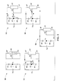
- FIG. 3 shows the effect of switching states on neutral point voltage deviation.
- PPP switching state
- the upper two switching devices ( FIG. 2 ) in each of the three converter legs are turned on, connecting the load terminals 47, 49, and 51 to the positive DC bus as shown in circuit 60. Since the neutral point 41 is left unconnected, this switching state does not affect neutral point voltage Vn.
- Circuit 62 shows the converter operation with a switching state POO (one leg with P switching state and the other two legs with O switching state as described in Table 1). In this state the three-phase load is connected between the positive DC bus and neutral point , and the neutral current in flows in through the neutral point causing Vn to increase.
- the switching state ONN causes Vn to decrease as shown in circuit 64.
- terminals 47, 49 and 51 are connected to the positive DC bus, the neutral point, and the negative bus, respectively.
- the neutral-point voltage Vn may rise or drop.
- switching state PNN as shown in circuit 68, the terminals are connected to the positive and negative DC buses. The neutral point is left unconnected and thus the neutral point voltage is not affected.
- the neutral point voltage varies and may not remain balanced at Vdc/2.
- FIG. 4 shows a detailed block diagram of a converter controller 50 for use in the configuration of FIG. 2 in accordance with one embodiment of the present invention.
- Controller 50 includes a DC link voltage regulator 82, a differential mode current regulator 84, a neutral point (NP) controller 86 and a PWM controller 88.
- DC link * voltage regulator 82 generates a d-domain reference current command signal i* d based on an error signal which is a difference between the reference or the desired total DC link voltage u * DC,tot' and the actual total DC link voltage u DC,tot as obtained by a comparator 90, for example.
- DC link voltage regulator 82 comprises a proportional-integral (PI) regulator.
- a q-domain reference current command signal i* q may be generated by a reactive power regulator 81 based on a difference between a desired amount of reactive power or a reference reactive power Q* and an actual reactive power Qa.
- Differential mode current regulator 84 receives d-q domain reference current command signals i* d , i * q and d-q domain actual current command signals i d , i q and uses those signals to generate d-q domain reference voltage command signals u* d and u* q based on the difference between the reference and the actual current command signals.
- actual current command signals i d , i q are determined from measured three phase a-b-c domain load currents i a , i b , i c by transforming them into d-q domain currents.
- Differential mode current regulator includes two PI regulators. One for d-domain currents i* d and i d for generating d domain reference voltage command signal u * d and the other one for q-domain currents i * q and i q for generating q domain reference voltage command signal u * q .
- d-q to a-b-c domain transformation matrices 92 and 94 may be used to transform d-q domain reference current command signals i * d , i * q and d-q domain reference voltage command signals u * d , u * q into the a-b-c domain reference current command signals i * a , i * b , i * c and a-b-c domain reference voltage command signals u * a , u * b , u * c , respectively, based on a phase angle ⁇ .
- phase angle ⁇ is generated by a phase locked loop (PLL) (not shown) based on three phase load voltages or grid voltages if the converter is connected to the power grid.
- PLL phase locked loop
- NP controller 86 generates a common mode reference voltage signal u * cm for compensating the DC link voltage unbalance.
- the common mode reference voltage signal u * cm is then further added to the a-b-c domain reference voltage command signals u * a , u * b , u * c before providing the combined voltage signal to PWM controller 88.
- the resultant signal of addition of u * a , u * b , u * c and u * cm is thus used by the multilevel converter controller to balance the neutral point voltage.
- NP controller 86 generates the common mode reference voltage signal u * cm based on d-domain reference current command signal i * d , a-b-c domain reference current command signals i * a , i * b , i * c , a-b-c domain reference voltage command signals u * a , u * b , u * c and differential DC link voltage signal ⁇ u dc as discussed below with respect to FIG. 5 .
- NP controller 86 may use measured load current signals i a , i b , i c rather than reference current command signals i * a , i * b , i * c for generating the common mode reference voltage signal.
- the above generated three phase duty cycles are then utilized to produce PWM pulses for individual switching devices of the multilevel converter.
- a sine triangular PWM or a space vector PWM is used for generating the PWM pulses.
- FIG. 5 shows a detailed block diagram of the NP controller 86 of FIG. 4 .
- NP controller 86 includes a Min-Max classifier 100 to determine instantaneous minimum, maximum, and medium current and voltage values, i u min , i u max , i umid , and u min , u max , u mid of the a-b-c domain reference current i * a , i * b , i * c and reference voltage u * a , u * b , u * c signals respectively.
- minimum, maximum, and medium values for a-b-c domain reference voltages may be -147V, 147V and 0V at a particular instant.
- the instantaneous minimum, maximum, and medium current and voltage values are then provided to a NP current pre-calculator 102 and a NP limit calculator 104.
- NP current pre-calculator determines the current that flows into the neutral point if no additional common mode reference voltage is injected to the reference voltage command signals. In other words, it determines the present neutral point current without disturbing the common mode reference that is being added to the a-b-c domain reference voltage command signals.
- the average value of neutral point current i * np, pre over a time period becomes zero if it is not modified.
- NP limit calculator 104 determines minimum and maximum limits for neutral point current signal i * np , pre , and common mode reference voltage signal u * cm .
- the limits are identified based on several constraints. For example, the amplitude of the common mode reference voltage is limited by the modulation index (MI) of the multilevel converter which indicates the peak line-to-line output voltage that can be generated by the multilevel converter and is generally lower than the total DC-link voltage at any instant.
- MI modulation index
- u DC , p + u min u * cm , max min ( u min - u DC , m . DC max , 1 - DC max . u DC , m + u max where DC max is a constant which indicates maximum duty cycle that can be achieved in the circuit and depends on circuit design.
- a proportional - integral (PI) regulator 110 generates a DC control signal g cm based on a differential DC link voltage signal ⁇ u dc after subtracting it from zero to indicate whether the differential DC link voltage is above or below zero.
- the differential DC link voltage is a difference between top capacitor voltage and the bottom capacitor voltage of the DC link.
- d domain reference current command signal i * d is used as a factor that could be used to modify the PI regulator 110 gain.
- the resulting DC control signal g cm will have values between +1 and -1 and is utilized by waveform corrector 106 along with maximum and minimum current limit signals for modifying the neutral point current signal * np , pre determined in equation 2 from NP current pre-calculator 102.
- Dynamic CM voltage regulator 108 generates the common mode reference voltage signal u * cm for compensating the DC link voltage unbalance based on the modified current signal i * np .
- the dynamic CM voltage regulator 108 includes a look-up table that provides the required CM reference voltage magnitude according to the modified current signal.
- the look up table will have voltage values within the maximum and minimum limit signals u * cm, max and u * cm, min determined in equations 3 and 4 respectively at that instant.
- the voltage values in the look up table vary depending on the load power factor.
- the curve between voltage values and the respective current values in the lookup table for a given power factor is partly linear and in most cases there is only one solution available. For example, at a load power factor of 0.9 the curve will be a flat line. In certain cases, there may be two solutions available. In these cases, the solution with lower amplitude is chosen as described in more detail in FIG. 7 .
- FIG. 6 shows neutral point current simulation plots 130 and 140 for two different power factors.
- horizontal axis 131 represents a reference vector angle in degree which is representative of time
- vertical axis 133 represents normalized current values in amperes.
- Curves 132 and 142 represent maximum neutral point current signals i * np
- max and curves 134 and 144 represent minimum neutral point current signals i * np, min .
- curves 136 and 146 represent neutral point current signals i * np
- FIG. 7 shows simulation plots 160, 162 and 164 for determining common mode voltage for three different power factors in accordance with an embodiment of the present invention.
- horizontal axis 161 represents common mode voltage in volts
- vertical axis 163 represents normalized modified neutral point current i * np / i peak , where i peak is the peak neutral point current.
- the vertical axis may directly be represented with only modified neutral point current.
- Plot 160 is for phase angle 209.7°
- plot 162 is for phase angle 59.7°
- plot 164 is for phase angle 149.7°.
- all the common mode voltage values for a given power factor or the phase angle and the neutral point current are stored in a lookup table. As described earlier, if there are two solutions as in plot 164 then the one with lower magnitude is selected. Thus, in plot 164, solution 168 which has lower magnitude compared to solution 169 is selected.
- FIG. 8 shows simulation plots 170 and 180 for total harmonic distortion (THD) in output currents.
- FFT Fast Fourier transform
- FIG. 8 shows simulation plots 170 and 180 for total harmonic distortion (THD) in output currents.
- FFT Fast Fourier transform
- plot 170 is for a multilevel converter operation without any NP controller
- FFT plot 180 is for a multilevel converter operation with a NP controller as described herein. Both plots are for zero power factor.
- FFT plot 170 shows that 2 nd and 4 th harmonics have significant amplitudes whereas FFT plot 180 shows that the harmonics are well suppressed.
- One of the advantages of the NP controller described herein is improved stability of three level converters even when operating at zero power factor.
- the NP controller further reduces the THD of output current and may reduce the cost of the DC link capacitors.
Abstract
Description
- This invention relates generally to multilevel converters and more specifically to a system and method for DC link voltage balancing in multilevel converters.
- Multilevel converters are generally used in high power industrial applications such as variable speed drive (VSD) systems or in energy conversion applications such as a solar (or photovoltaic) power generation systems, wind turbine generators and marine and hydrokinetic power generation systems. One example of a multi-level converter is a neutral point clamped (NPC) converter. A three level converter, for example, typically includes two capacitor voltages in series with a center tap as the neutral and two phase legs each comprising two pairs of switching devices in series. In one embodiment, each switching device comprises an anti-parallel connection of a unidirectional electronic switching device, such as an insulated gate bipolar transistor or an insulated gate commutated thyristor, and a diode, such as a free-wheeling diode.
- DC link voltage balancing is a challenge when operating three level neutral clamped converters (NPC). DC link voltage unbalance may overstress the capacitors and switching devices and cause over voltage and under voltage trips during the operation of the converter. In severe DC link voltage unbalance conditions, one capacitor may become fully charged to the full DC-link voltage such that stress on the capacitor and the switching devices is doubled and the output waveforms become two level rather than three-level. DC link voltage unbalance also causes an increase in output voltage total harmonic distortion (THD) and may cause the control loop to become unstable.
- One of the methods of compensating DC link voltage unbalance is utilizing measured DC-link voltages for pulse width modulation (PWM) control of the three level converter. This method, however, includes additional expense, does not compensate for steady-error in DC link voltage, and also results in high THD in the output voltage and injects active 2nd harmonic current at AC side. Another method of compensating DC link voltage unbalance is to use zero sequence voltage or DC bias voltage injection. However, this method also has high THD in the output voltage at some operation points and becomes unstable at low power factors.
- Therefore, it is desirable to provide a method and a system that will address the foregoing issues.
- In accordance with an embodiment of the present invention, a control system for controlling a multilevel converter is provided. The control system includes a differential mode current regulator to generate reference voltage command signals based on a difference between reference current command signals and actual current command signals. The system also includes a neutral point (NP) controller to determine a modified neutral point current signal in response to a DC link voltage unbalance and to use the modified neutral point current signal to generate a common mode reference voltage signal. The system further includes a PWM controller to generate switching pulses for the multilevel converter based on the reference voltage command signals and the common mode reference voltage signals.
- In accordance with another embodiment of the present invention, a method of controlling a multilevel converter is provided. The method includes (a) generating reference voltage command signals based on a difference between reference current command signals and actual current command signals. The method also includes (b) in response to a voltage unbalance on a DC link of the multi-level converter, (i) using the reference voltage command signals and reference current command signals for generating a modified neutral point current signal to compensate for the DC link voltage unbalance, (ii) using the modified neutral point current signal for generating a common mode reference voltage signal; and (iii) generating switching pulses for the multilevel converter based on summation of reference voltage command signals and the common mode reference voltage signal.
- In accordance with yet another embodiment of the present invention, a multilevel converter including a plurality of phase legs each having at least two inner switching devices, at least two outer switching devices, at least two clamping diodes and a split DC link is provided. The multilevel converter also includes a control system for controlling the multilevel converter. The control system includes a differential mode current regulator to generate reference voltage command signals based on a difference between reference current command signals and actual current command signals. The system also includes a neutral point (NP) controller to determine a modified neutral point current signal in response to a DC link voltage unbalance and to use the modified neutral point current signal to generate a common mode reference voltage signal. The system further includes a PWM controller to generate switching pulses for the multilevel converter based on the reference voltage command signals and the common mode reference voltage signals.
- Various features, aspects, and advantages of the present invention will become better understood when the following detailed description is read with reference to the accompanying drawings in which like characters represent like parts throughout the drawings, wherein:
-
FIG. 1 is a circuit diagram of one leg of a conventional neutral point clamped multilevel converter and its output waveform; -
FIG. 2 is a circuit diagram of a three phase three level converter for use in accordance with an embodiment of the present invention; -
FIG. 3 is a schematic representation of different load connections at different switching states for the embodiment ofFIG. 2 ; -
FIG. 4 is a detailed block diagram of a converter controller in accordance with an embodiment of the present invention; -
FIG. 5 is detailed block diagram of a neutral point (NP) controller in accordance with an embodiment of the present invention; -
FIG. 6 is a graphical representation of an NPC current simulation plots; -
FIG. 7 is a graphical representation of plots for determining common voltage signal; and -
FIG. 8 is a graphical representation of output current total harmonic distortion simulation plots. -
FIG. 1 illustrates a schematic 10 of one leg or one phase of a conventional neutral point clamped (NPC) or diode clamped three level converter and itsoutput waveform 12. Oneleg 14 of the three-level converter includes fourswitching devices clamping diodes neutral point 28 ofDC link 30. Switchingdevice 16 is complementary to switchingdevice 20 so that, when switchingdevice 16 is gated on, switchingdevice 20 is gated off and vice versa. Similarly, switchingdevices - In operation, each leg of the NPC three level converter has three switching stages P, O, and N respectively. The three switching stages and the respective output voltages are given in following table:
Table 1 Switching Stage Switching Device 16 Switching Device 18Switching Device 20Switching Device 22Voltage V3 P ON ON OFF OFF +Vdc/2 O OFF ON ON OFF 0 N OFF OFF ON ON -Vdc/2 - In the first switching stage P, switching
devices devices devices devices devices devices waveform 12. Thus, it can be seen that the phase voltage V3 has three levels Vdc/2, -Vdc/2, and 0. When all three legs of the NPC three-phase converter are combined, then the resulting line to line voltages have five levels namely Vdc, Vdc/2, 0, -Vdc/2 and -Vdc. - The
converter leg 14 ofFIG. 1 may be modified so as to increase the number of voltage levels to any level depending on the circuit topology and number of switching devices and diodes in the circuit. As the number of levels in the converter increases, the output waveform of the converter approaches a pure sine wave, resulting in lower harmonics in the output voltage. In general, the number of switching stages can be higher than three as switching devices may not be gated on if the corresponding free-wheeling diode is going to conduct current. This operation mode does not affect the number of levels of the output phase voltage. -
FIG. 2 illustrates a schematic 40 of a three phase three level converter for use in accordance with an embodiment of the present invention. Theconverter 40 includes asplit DC link 42 with aneutral point 41 andcapacitors switching legs output terminals phase load 61 is connected across the threephase output terminals converter controller 50 provides switching pulse commands to switching devices of theswitching legs output terminals -
FIG. 3 shows the effect of switching states on neutral point voltage deviation. When the converter is operated with a switching state [PPP], in other words, when all legs are in a P switching state, the upper two switching devices (FIG. 2 ) in each of the three converter legs are turned on, connecting theload terminals circuit 60. Since theneutral point 41 is left unconnected, this switching state does not affect neutral pointvoltage Vn. Circuit 62 shows the converter operation with a switching state POO (one leg with P switching state and the other two legs with O switching state as described in Table 1). In this state the three-phase load is connected between the positive DC bus and neutral point , and the neutral current in flows in through the neutral point causing Vn to increase. In contrast, the switching state ONN causes Vn to decrease as shown incircuit 64. For switching state PON incircuit 66,terminals circuit 68, the terminals are connected to the positive and negative DC buses. The neutral point is left unconnected and thus the neutral point voltage is not affected. Thus, depending on the switching states and the load current, the neutral point voltage varies and may not remain balanced at Vdc/2. -
FIG. 4 shows a detailed block diagram of aconverter controller 50 for use in the configuration ofFIG. 2 in accordance with one embodiment of the present invention.Controller 50 includes a DClink voltage regulator 82, a differential modecurrent regulator 84, a neutral point (NP)controller 86 and aPWM controller 88. DC link *voltage regulator 82, generates a d-domain reference current command signal i*d based on an error signal which is a difference between the reference or the desired total DC link voltage u* DC,tot' and the actual total DC link voltage uDC,tot as obtained by acomparator 90, for example. In one embodiment, DClink voltage regulator 82 comprises a proportional-integral (PI) regulator. In one embodiment, a q-domain reference current command signal i*q may be generated by areactive power regulator 81 based on a difference between a desired amount of reactive power or a reference reactive power Q* and an actual reactive power Qa. Differential modecurrent regulator 84 receives d-q domain reference current command signals i*d, i* q and d-q domain actual current command signals id, iq and uses those signals to generate d-q domain reference voltage command signals u*d and u*q based on the difference between the reference and the actual current command signals. In one embodiment, actual current command signals id , iq are determined from measured three phase a-b-c domain load currents ia, ib, ic by transforming them into d-q domain currents. Differential mode current regulator includes two PI regulators. One for d-domain currents i*d and id for generating d domain reference voltage command signal u* d and the other one for q-domain currents i* q and iq for generating q domain reference voltage command signal u* q . - As further shown in
FIG. 4 , d-q to a-b-cdomain transformation matrices NP controller 86 generates a common mode reference voltage signal u* cm for compensating the DC link voltage unbalance. The common mode reference voltage signal u* cm is then further added to the a-b-c domain reference voltage command signals u* a, u* b, u* c before providing the combined voltage signal toPWM controller 88. The resultant signal of addition of u* a , u* b , u* c and u* cm is thus used by the multilevel converter controller to balance the neutral point voltage. -
NP controller 86 generates the common mode reference voltage signal u* cm based on d-domain reference current command signal i* d , a-b-c domain reference current command signals i* a , i* b , i* c , a-b-c domain reference voltage command signals u* a, u* b, u* c and differential DC link voltage signal Δudc as discussed below with respect toFIG. 5 . In one embodiment,NP controller 86 may use measured load current signals ia , ib , ic rather than reference current command signals i* a , i* b , i* c for generating the common mode reference voltage signal.PWM controller 88 also receives measured half DC-link voltages i.e., the top capacitor voltage or the positive bus DC link voltage with respect to neutral point u DC,p and the bottom capacitor voltage or the negative bus DC link voltage with respect to neutral point u DC,m and generates three phase duty cycle signals DC a...c for the three level converter given by:
- The above generated three phase duty cycles are then utilized to produce PWM pulses for individual switching devices of the multilevel converter. In one embodiment, a sine triangular PWM or a space vector PWM is used for generating the PWM pulses.
-
FIG. 5 shows a detailed block diagram of theNP controller 86 ofFIG. 4 .NP controller 86 includes a Min-Max classifier 100 to determine instantaneous minimum, maximum, and medium current and voltage values, i u min, i u max, iumid, and u min, u max, umid of the a-b-c domain reference current i* a , i* b , i* c and reference voltage u* a , u* b , u* c signals respectively. For example, minimum, maximum, and medium values for a-b-c domain reference voltages may be -147V, 147V and 0V at a particular instant. The instantaneous minimum, maximum, and medium current and voltage values are then provided to a NP current pre-calculator 102 and aNP limit calculator 104. - NP current pre-calculator determines the current that flows into the neutral point if no additional common mode reference voltage is injected to the reference voltage command signals. In other words, it determines the present neutral point current without disturbing the common mode reference that is being added to the a-b-c domain reference voltage command signals. The neutral point current signal i* np, pre is calculated by following equation:

- The average value of neutral point current i* np, pre over a time period becomes zero if it is not modified.
-
NP limit calculator 104 determines minimum and maximum limits for neutral point current signal i* np, pre , and common mode reference voltage signal u* cm. The limits are identified based on several constraints. For example, the amplitude of the common mode reference voltage is limited by the modulation index (MI) of the multilevel converter which indicates the peak line-to-line output voltage that can be generated by the multilevel converter and is generally lower than the total DC-link voltage at any instant. In one embodiment, the maximum and minimum limits u* cm, max and u* cm, min for the common mode reference voltage are given by:

where DC max is a constant which indicates maximum duty cycle that can be achieved in the circuit and depends on circuit design. Similarly, maximum, medium, and minimum limits i* np, max, i* np, mid , and i* np, min for the neutral point current signal may be given by
where I, II and III refers to min, mid and max respectively. The maximum and minimum current limit and voltage limit signals are then provided to awaveform corrector 106 and a dynamic common mode (CM)voltage regulator 108. - A proportional - integral (PI)
regulator 110 generates a DC control signal gcm based on a differential DC link voltage signal Δudc after subtracting it from zero to indicate whether the differential DC link voltage is above or below zero. The differential DC link voltage is a difference between top capacitor voltage and the bottom capacitor voltage of the DC link. In an optional embodiment, d domain reference current command signal i* d is used as a factor that could be used to modify thePI regulator 110 gain. The resulting DC control signal gcm will have values between +1 and -1 and is utilized bywaveform corrector 106 along with maximum and minimum current limit signals for modifying the neutral point current signal * np, pre determined inequation 2 from NPcurrent pre-calculator 102. If no DC-link unbalance is detected, that is, if Δudc =0 or gcm =0, then the neutral point current signal i* np , pre is not changed. Otherwise, the neutral point current signal i* np, pre will be modified and the modified neutral point current signal i* np will be given as:
- It can be seen from the above equation that if DC control signal gcm is zero (if there is no voltage unbalance) then the neutral point current signal need not be modified * and hence it remains i* np, pre. However, if gcm is not zero, then the current * i* np, pre is modified or regulated based on the DC control signal gcm . Further, it is ensured that the modified current signal i* np is within the maximum and minimum * * limits i* np, max and i* np, min determined in equations 5 and 6 respectively.
- Dynamic
CM voltage regulator 108 generates the common mode reference voltage signal u* cm for compensating the DC link voltage unbalance based on the modified current signal i* np. In one embodiment, the dynamicCM voltage regulator 108 includes a look-up table that provides the required CM reference voltage magnitude according to the modified current signal. At a particular instant, for a given current signal i* np, the look up table will have voltage values within the maximum and minimum limit signals u* cm, max and u* cm, min determined inequations 3 and 4 respectively at that instant. The voltage values in the look up table vary depending on the load power factor. The curve between voltage values and the respective current values in the lookup table for a given power factor is partly linear and in most cases there is only one solution available. For example, at a load power factor of 0.9 the curve will be a flat line. In certain cases, there may be two solutions available. In these cases, the solution with lower amplitude is chosen as described in more detail inFIG. 7 . -
FIG. 6 shows neutral point current simulation plots 130 and 140 for two different power factors.Plot 130 is for a power factor of 0.9 and the DC control signal gcm =0.5, whereasplot 140 is for same power factor but for gcm =1. In bothplots horizontal axis 131 represents a reference vector angle in degree which is representative of time, andvertical axis 133 represents normalized current values in amperes.Curves plot 140 that when gcm =1, i*np, pre= i* np, max as given byequation 7 and thus, thecurves -
FIG. 7 showssimulation plots plots horizontal axis 161 represents common mode voltage in volts, andvertical axis 163 represents normalized modified neutral point current i* np /ipeak , where ipeak is the peak neutral point current. In one embodiment, the vertical axis may directly be represented with only modified neutral point current.Plot 160 is for phase angle 209.7°,plot 162 is for phase angle 59.7° andplot 164 is for phase angle 149.7°. It can be seen fromplots solution plot 164 that there are twosolutions solutions plot 164 then the one with lower magnitude is selected. Thus, inplot 164,solution 168 which has lower magnitude compared tosolution 169 is selected. -
FIG. 8 showssimulation plots plot 170 is for a multilevel converter operation without any NP controller whereasFFT plot 180 is for a multilevel converter operation with a NP controller as described herein. Both plots are for zero power factor.FFT plot 170 shows that 2nd and 4th harmonics have significant amplitudes whereasFFT plot 180 shows that the harmonics are well suppressed. - One of the advantages of the NP controller described herein is improved stability of three level converters even when operating at zero power factor. The NP controller further reduces the THD of output current and may reduce the cost of the DC link capacitors.
- While only certain features of the invention have been illustrated and described herein, many modifications and changes will occur to those skilled in the art. It is, therefore, to be understood that the appended claims are intended to cover all such modifications and changes as fall within the true spirit of the invention.
- Various aspects and embodiments of the present invention are defined by the following numbered clauses:
- 1. A control system for controlling a multilevel converter, the control system comprising:
- a differential mode current regulator for generating reference voltage command signals based on a difference between reference current command signals and actual current command signals;
- a neutral point (NP) controller for determining a modified neutral point current signal in response to a DC link voltage unbalance and using the modified neutral point current signal to generate a common mode reference voltage signal; and
- a PWM controller for generating switching pulses for the multilevel converter based on the reference voltage command signals and the common mode reference voltage signal.
- 2. The control system of
clause 1, wherein the reference current command signals comprise d-q domain reference current command signals and the reference voltage command signals comprise d-q domain reference voltage command signals. - 3. The control system of any preceding clause, further comprising a DC link voltage regulator for generating the d-domain reference current command signal based on a difference between a reference DC link voltage signal and a desired DC link voltage signal and a reactive power regulator for generating the q-domain reference current command signal based on a difference between a reference reactive power signal and a desired reactive power signal.
- 4. The control system of any preceding clause, comprising transformation matrices for transforming the d-q domain reference current command signals into a-b-c domain reference current command signals and d-q domain reference voltage command signals into a-b-c domain reference voltage command signals.
- 5. The control system of any preceding clause, wherein the NP controller comprises a min-max classifier for determining instantaneous minimum, medium, and maximum voltage and current signals among reference current command signals and reference voltage command signals or among measured current command signals and reference voltage command signals.
- 6. The control system of any preceding clause, wherein the NP controller comprises an NP current pre-calculator for generating a neutral point current signal based on the instantaneous minimum, medium, and maximum voltage and current signals.
- 7. The control system of any preceding clause, further comprising a NP limit calculator for determining minimum and maximum limits for the neutral point current signal and the common mode reference voltage signal.
- 8. The control system of any preceding clause, further comprising a waveform corrector for generating the modified neutral point current signal based on the minimum and maximum limits for the neutral point current signal and a DC control signal.
- 9. The control system of any preceding clause, wherein the DC control signal is generated by a PI regulator based on a differential DC link voltage signal.
- 10. The control system of any preceding clause, wherein the modified neutral point current signal is equal to the neutral point current signal when the DC control signal is zero.
- 11. The control system of any preceding clause, further comprising a dynamic common mode (CM) voltage calculator for generating the common mode reference voltage signal based on the modified neutral point current and minimum and maximum limits for the neutral point current signal and the common mode reference voltage signal.
- 12. The control system of any preceding clause, wherein the dynamic CM voltage calculator comprises a look-up table for providing the CM reference voltage signal magnitude according to the modified current signal and a load power factor.
- 13. A method of controlling a multilevel converter comprising:
- (a) generating reference voltage command signals based on a difference between reference current command signals and actual current command signals;
- (b) in response to a voltage unbalance on a DC link of the multi-level converter,
- (i) using the reference voltage command signals and reference current command signals for generating a modified neutral point current signal to compensate for the DC link voltage unbalance;
- (ii) using the modified neutral point current signal for generating a common mode reference voltage signal; and
- (iii) generating switching pulses for the multilevel converter based on summation of reference voltage command signals and the common mode reference voltage signal.
- 14. The method of any preceding clause, wherein the reference current command signals comprise d-q domain reference current command signals and the reference voltage command signals comprise d-q domain reference voltage command signals.
- 15. The method of any preceding clause, wherein the d-domain reference current command signal is based on a difference between a reference DC link voltage signal and a desired DC link voltage signal and the q-domain reference current command signal is based on a difference between a reference reactive power signal and a desired reactive power signal.
- 16. The method of any preceding clause, wherein generating the modified neutral point current signal comprises modifying a neutral point current signal based on the minimum and maximum limits for the neutral point current signal and a DC control signal.
- 17. The method of any preceding clause, wherein the neutral point current signal is generated based on instantaneous minimum, medium, and maximum reference current command signals and reference voltage command signals.
- 18. The method of any preceding clause, wherein the DC control signal is generated by based on a differential DC link voltage signal.
- 19. The method of any preceding clause, wherein the common mode reference voltage signal is generated based on a load power factor and the minimum and maximum limits for the neutral point current signal and the common mode reference voltage signal.
- 20. A multilevel converter comprising:
- a plurality of phase legs each having at least two inner switching devices, at least two outer switching devices, at least two clamping diodes and a split DC link; and
- a control system for controlling the multilevel converter comprising
- a differential mode current regulator for generating reference voltage command signals based on a difference between reference current command signals and actual current command signals;
- a neutral point (NP) controller for determining a modified neutral point current signal in response to a DC link voltage unbalance and using the modified neutral point current signal to generate ; and
- a PWM controller for generating switching pulses for the multilevel converter based on the reference voltage command signals and the common mode reference voltage signal.
Claims (10)
- A control system (50) for controlling a multilevel converter (40), the control system (50) comprising:a differential mode current regulator (84) for generating reference voltage command signals based on a difference between reference current command signals and actual current command signals;a neutral point (NP) controller (86) for determining a modified neutral point current signal in response to a DC link voltage unbalance and using the modified neutral point current signal to generate a common mode reference voltage signal; anda PWM controller (88) for generating switching pulses for the multilevel converter (40) based on the reference voltage command signals and the common mode reference voltage signal.
- The control system (50) of claim 1, wherein the reference current command signals comprise d-q domain reference current command signals and the reference voltage command signals comprise d-q domain reference voltage command signals.
- The control system (50) of any preceding claim, further comprising a DC link voltage regulator (82) for generating the d-domain reference current command signal based on a difference between a reference DC link voltage signal and a desired DC link voltage signal and an reactive power regulator (81) for generating the q-domain reference current command signal based on a difference between a reference reactive power signal and a desired reactive power signal.
- The control system (50) of any preceding claim, wherein the NP controller (86) comprises a min-max classifier (100) for determining instantaneous minimum, medium, and maximum voltage and current signals among reference current command signals and reference voltage command signals or among measured current command signals and reference voltage command signals.
- The control system (50) of any preceding claim, wherein the NP controller (86) comprises an NP current pre-calculator (102) for generating a neutral point current signal based on the instantaneous minimum, medium, and maximum voltage and current signals.
- The control system (50) of any preceding claim, further comprising a NP limit calculator (104) for determining minimum and maximum limits for the neutral point current signal and the common mode reference voltage signal.
- The control system (50) of any preceding claim, further comprising a waveform corrector (106) for generating the modified neutral point current signal based on the minimum and maximum limits for the neutral point current signal and a DC control signal.
- The control system (50) of claim 6 or claim 7, further comprising a dynamic common mode (CM) voltage calculator (108) for generating the common mode reference voltage signal based on the modified neutral point current and minimum and maximum limits for the neutral point current signal and the common mode reference voltage signal.
- A method of controlling a multilevel converter (40) comprising:(a) generating (84) reference voltage command signals based on a difference between reference current command signals and actual current command signals;(b) in response to a voltage unbalance on a DC link of the multi-level converter,(i) using the reference voltage command signals and reference current command signals for generating (86) a modified neutral point current signal to compensate for the DC link voltage unbalance;(ii) using the modified neutral point current signal for generating (108) a common mode reference voltage signal; and(iii) generating (88) switching pulses for the multilevel converter based on summation of reference voltage command signals and the common mode reference voltage signal.
- A multilevel converter (40) comprising:a plurality of phase legs (44, 46, 48) each having at least two inner switching devices, at least two outer switching devices, at least two clamping diodes and a split DC link; anda control system (50) for controlling the multilevel converter comprising
a differential mode current regulator (84) for generating reference voltage command signals based on a difference between reference current command signals and actual current command signals;
a neutral point (NP) controller (86) for determining a modified neutral point current signal in response to a DC link voltage unbalance and using the modified neutral point current signal to generate; and
a PWM controller (88) for generating switching pulses for the multilevel converter based on the reference voltage command signals and the common mode reference voltage signal.
Applications Claiming Priority (1)
| Application Number | Priority Date | Filing Date | Title |
|---|---|---|---|
| US12/893,015 US8441820B2 (en) | 2010-09-29 | 2010-09-29 | DC-link voltage balancing system and method for multilevel converters |
Publications (3)
| Publication Number | Publication Date |
|---|---|
| EP2437389A2 true EP2437389A2 (en) | 2012-04-04 |
| EP2437389A3 EP2437389A3 (en) | 2015-05-27 |
| EP2437389B1 EP2437389B1 (en) | 2018-04-18 |
Family
ID=44142727
Family Applications (1)
| Application Number | Title | Priority Date | Filing Date |
|---|---|---|---|
| EP11181455.4A Active EP2437389B1 (en) | 2010-09-29 | 2011-09-15 | DC-link voltage balancing system and method for multilevel converters |
Country Status (4)
| Country | Link |
|---|---|
| US (1) | US8441820B2 (en) |
| EP (1) | EP2437389B1 (en) |
| CN (1) | CN102437760B (en) |
| DK (1) | DK2437389T3 (en) |
Cited By (2)
| Publication number | Priority date | Publication date | Assignee | Title |
|---|---|---|---|---|
| DE102013108670A1 (en) * | 2013-08-09 | 2015-02-12 | Ge Energy Power Conversion Gmbh | Method and device for operating a power converter |
| EP3208931A4 (en) * | 2014-10-20 | 2018-05-23 | Meidensha Corporation | Three-phase neutral-point-clamped power conversion device |
Families Citing this family (61)
| Publication number | Priority date | Publication date | Assignee | Title |
|---|---|---|---|---|
| US8411474B2 (en) * | 2010-04-30 | 2013-04-02 | General Electric Company | System and method for protection of a multilevel converter |
| JP4877411B1 (en) * | 2010-09-30 | 2012-02-15 | ダイキン工業株式会社 | Link voltage measurement method |
| US11901810B2 (en) | 2011-05-08 | 2024-02-13 | Koolbridge Solar, Inc. | Adaptive electrical power distribution panel |
| US11460488B2 (en) | 2017-08-14 | 2022-10-04 | Koolbridge Solar, Inc. | AC electrical power measurements |
| US8937822B2 (en) | 2011-05-08 | 2015-01-20 | Paul Wilkinson Dent | Solar energy conversion and utilization system |
| US8570776B2 (en) * | 2011-05-27 | 2013-10-29 | Alstom Technology Ltd | Method and device for determining a control scheme for an active power filter |
| CN103875147B (en) | 2011-10-14 | 2017-08-25 | Abb技术有限公司 | Multi-level converter and for control include balancing cell voltages multi-level converter method |
| DE102012101156A1 (en) * | 2012-02-14 | 2013-08-14 | Lti Drives Gmbh | Network feed device, energy supply system and method for operating a network feed device |
| US9444320B1 (en) * | 2012-04-16 | 2016-09-13 | Performance Controls, Inc. | Power controller having active voltage balancing of a power supply |
| JP6225418B2 (en) * | 2012-04-19 | 2017-11-08 | 株式会社明電舎 | 3-level inverter controller |
| ES2718807T3 (en) * | 2012-06-07 | 2019-07-04 | Abb Research Ltd | Zero sequence damping and voltage balancing procedure in a three-level converter with split DC link capacitors and virtually grounded LCL filter |
| WO2014011706A1 (en) * | 2012-07-09 | 2014-01-16 | Inertech Ip Llc | Transformerless multi-level medium-voltage uninterruptible power supply (ups) systems and methods |
| US9214874B2 (en) * | 2012-07-31 | 2015-12-15 | Yashomani Y. Kolhatkar | Intelligent level transition systems and methods for transformerless uninterruptible power supply |
| US8934276B2 (en) * | 2012-08-16 | 2015-01-13 | Mitsubishi Electric Research Laboratories, Inc. | DC-link voltage balancing control for multilevel inverters |
| US20140103650A1 (en) * | 2012-10-11 | 2014-04-17 | Hamilton Sundstrand Corporation | Dual-dc bus starter/generator |
| US9755546B2 (en) * | 2012-11-21 | 2017-09-05 | Otis Elecator Company | PWM controlled neutral point clamped multilevel converter |
| WO2014083214A1 (en) * | 2012-11-30 | 2014-06-05 | Ingeteam Power Technology, S.A. | Switching stage, energy conversion circuit, and conversion stage for wind turbines comprising the energy conversion circuit |
| US9722511B2 (en) * | 2012-12-07 | 2017-08-01 | General Electric Company | Systems and methods for controlling an electrical power supply |
| US9941813B2 (en) | 2013-03-14 | 2018-04-10 | Solaredge Technologies Ltd. | High frequency multi-level inverter |
| US9209626B2 (en) * | 2013-06-25 | 2015-12-08 | Renewable Power Conversion, Inc. | Parallelable three-phase photovoltaic power converter |
| CN104283432B (en) | 2013-07-03 | 2017-12-26 | 通用电气公司 | Joint common-mode voltage injected system and method |
| CN103414366B (en) * | 2013-07-24 | 2016-06-08 | 西安龙腾新能源科技发展有限公司 | The control method of DC side neutral-point potential balance in NPC three-level structure |
| CN104348342B (en) | 2013-08-02 | 2019-05-31 | 通用电气公司 | Electrical conversion systems and method |
| US9252681B2 (en) * | 2013-08-30 | 2016-02-02 | General Electric Company | Power converter with a first string having controllable semiconductor switches and a second string having switching modules |
| EP2849331B1 (en) * | 2013-09-11 | 2020-02-12 | ABB Schweiz AG | Method and apparatus for balancing voltages of multi-level inverter DC link |
| US9461536B2 (en) * | 2013-11-27 | 2016-10-04 | Infineon Technologies Austria Ag | Digital controller with nested loops for switched mode power converter |
| CN105830332B (en) * | 2013-12-18 | 2019-10-18 | 奥的斯电梯公司 | Control strategy for more level line regenerative drivers |
| US9755551B2 (en) * | 2014-01-06 | 2017-09-05 | Toshiba Mitsubishi-Electric Industrial Systems Corporation | Power conversion device |
| WO2015108614A1 (en) * | 2014-01-15 | 2015-07-23 | Abb Technology Ag | Modular, multi-channel, interleaved power converters |
| CN104811073B (en) * | 2014-01-24 | 2019-05-31 | 通用电气能源电能变换科技有限公司 | Converter module, device, system and correlation technique |
| US9318974B2 (en) | 2014-03-26 | 2016-04-19 | Solaredge Technologies Ltd. | Multi-level inverter with flying capacitor topology |
| US9555711B2 (en) * | 2014-06-03 | 2017-01-31 | Hamilton Sundstrand Corporation | Power converters |
| US9590521B2 (en) * | 2014-07-28 | 2017-03-07 | Hamilton Sundstrand Corporation | Power converters for aircraft starter/generators |
| CN104158429B (en) * | 2014-08-27 | 2017-04-19 | 阳光电源股份有限公司 | Three-level photovoltaic inverter pulse width modulation method and modulator |
| US9515574B2 (en) * | 2014-11-17 | 2016-12-06 | General Electric Company | Modular embedded multi-level converter with midpoint balancing |
| US9755545B2 (en) * | 2014-11-21 | 2017-09-05 | General Electric Company | System and method for unified common mode voltage injection |
| DE102014224371A1 (en) * | 2014-11-28 | 2016-06-02 | Robert Bosch Gmbh | Battery system with a hybrid battery and an NPC inverter connected to the battery on the input side and method for operating an NPC inverter connected on the input side with a hybrid battery |
| JP6426462B2 (en) * | 2014-12-24 | 2018-11-21 | 株式会社東芝 | Power converter and control method thereof |
| US9742311B2 (en) * | 2015-10-02 | 2017-08-22 | Hamilton Sundstrand Corporation | Systems and methods for controlling inverters |
| JP6538544B2 (en) * | 2015-12-22 | 2019-07-03 | 東芝三菱電機産業システム株式会社 | Self-excited reactive power compensator |
| JP6538542B2 (en) * | 2015-12-22 | 2019-07-03 | 東芝三菱電機産業システム株式会社 | Self-excited reactive power compensator |
| JP6131360B1 (en) * | 2016-03-28 | 2017-05-17 | 三菱電機エンジニアリング株式会社 | Power converter |
| US9970417B2 (en) * | 2016-04-14 | 2018-05-15 | General Electric Company | Wind converter control for weak grid |
| JP6658369B2 (en) * | 2016-07-13 | 2020-03-04 | オムロン株式会社 | Power converter |
| CN106253726B (en) * | 2016-08-04 | 2018-09-07 | 中国船舶重工集团公司第七一九研究所 | A kind of three-level inverter direct current neutral-point voltage balance method |
| US10211672B2 (en) * | 2016-10-13 | 2019-02-19 | Schneider Electric It Corporation | DC-link bus balancer |
| US9979291B2 (en) * | 2016-10-26 | 2018-05-22 | Futurewei Technologies, Inc. | Inverter apparatus |
| CN106533236B (en) * | 2016-12-15 | 2018-10-16 | 电子科技大学 | A kind of minimum switch losses implementation method of three-level inverter |
| CN106558977B (en) * | 2017-01-16 | 2018-09-28 | 阳光电源股份有限公司 | Three-phase three-wire system inverter and its output current control method and control system |
| EP3393034A1 (en) | 2017-04-21 | 2018-10-24 | GE Energy Power Conversion Technology Limited | Controlling a back-to-back three-level converter with midpoint voltage ripple compensation |
| JP7005417B2 (en) * | 2018-04-13 | 2022-01-21 | 株式会社東芝 | Power converter and control method of power converter |
| US10826381B2 (en) * | 2018-04-17 | 2020-11-03 | Abb Schweiz Ag | Method and control system for zero-sequence current compensation for ground current reduction |
| KR102109574B1 (en) * | 2018-05-31 | 2020-05-12 | 엘에스일렉트릭(주) | Apparatus for controlling inverter |
| EP3687059A1 (en) * | 2019-01-22 | 2020-07-29 | Siemens Aktiengesellschaft | Operation of switching elements of a multi-level energy converter |
| CN111342688B (en) * | 2019-12-20 | 2021-04-20 | 樊蓉 | Four-level converter voltage balance modulation method |
| US11387765B2 (en) * | 2020-03-13 | 2022-07-12 | Hamilton Sundstrand Corporation | Speed based gain correction for three level inverter midpoint control |
| US11456680B2 (en) | 2020-05-08 | 2022-09-27 | Hamilton Sundstrand Corporation | Over-modulation pulse width modulation with maximum output and minimum harmonics |
| CN112104248B (en) * | 2020-09-21 | 2022-11-25 | 国网黑龙江省电力有限公司绥化供电公司 | Control method of three-level NPC converter |
| US11258387B1 (en) * | 2020-10-30 | 2022-02-22 | General Electric Renovables Espana, S.L. | System and method for neutral point balancing for back-to-back voltage source converters |
| CN114070028B (en) * | 2021-11-19 | 2023-09-22 | 新风光电子科技股份有限公司 | Voltage equalizing control method of cascaded bidirectional converter device |
| CN117318475B (en) * | 2023-11-23 | 2024-01-30 | 京清数电(北京)技术有限公司 | Energy storage converter, control method and device thereof and readable storage medium |
Family Cites Families (13)
| Publication number | Priority date | Publication date | Assignee | Title |
|---|---|---|---|---|
| JP3229897B2 (en) | 1992-04-13 | 2001-11-19 | 三菱電機株式会社 | Three-level three-phase inverter device |
| US5790396A (en) * | 1995-12-19 | 1998-08-04 | Kabushiki Kaisha Toshiba | Neutral point clamped (NPC) inverter control system |
| US5852558A (en) | 1997-06-20 | 1998-12-22 | Wisconsin Alumni Research Foundation | Method and apparatus for reducing common mode voltage in multi-phase power converters |
| US6337804B1 (en) * | 2000-09-26 | 2002-01-08 | General Electric Company | Multilevel PWM voltage source inverter control at low output frequencies |
| ATE344983T1 (en) * | 2003-09-08 | 2006-11-15 | Abb Research Ltd | METHOD FOR BALANCED A DC VOLTAGE CIRCUIT OF A CONVERTER CIRCUIT FOR SWITCHING THREE VOLTAGE LEVELS |
| US7196919B2 (en) | 2005-03-25 | 2007-03-27 | Tyco Electronics Power Systems, Inc. | Neutral point controller, method of controlling and rectifier system employing the controller and the method |
| US7495938B2 (en) | 2005-04-15 | 2009-02-24 | Rockwell Automation Technologies, Inc. | DC voltage balance control for three-level NPC power converters with even-order harmonic elimination scheme |
| US7573732B2 (en) | 2007-05-25 | 2009-08-11 | General Electric Company | Protective circuit and method for multi-level converter |
| CN101420185A (en) * | 2008-10-15 | 2009-04-29 | 徐州中矿大传动与自动化有限公司 | Controlling method for three-level frequency transformer |
| US8144490B2 (en) * | 2009-11-10 | 2012-03-27 | General Electric Company | Operation of a three level converter |
| US8228695B2 (en) * | 2009-11-16 | 2012-07-24 | General Electric Company | Multilevel converter operation |
| CN101753044B (en) * | 2010-01-26 | 2012-06-27 | 北方工业大学 | Three-level midpoint potential balance control method based on zero-sequence voltage injection |
| BR112013015894A2 (en) * | 2010-12-22 | 2019-09-10 | Ge Energy Power Conversion Technology Limited | method for compensating voltages in a capacitor group of an electronic device and compensation circuit |
-
2010
- 2010-09-29 US US12/893,015 patent/US8441820B2/en active Active
-
2011
- 2011-09-15 EP EP11181455.4A patent/EP2437389B1/en active Active
- 2011-09-15 DK DK11181455.4T patent/DK2437389T3/en active
- 2011-09-28 CN CN201110309637.5A patent/CN102437760B/en active Active
Non-Patent Citations (1)
| Title |
|---|
| None |
Cited By (4)
| Publication number | Priority date | Publication date | Assignee | Title |
|---|---|---|---|---|
| DE102013108670A1 (en) * | 2013-08-09 | 2015-02-12 | Ge Energy Power Conversion Gmbh | Method and device for operating a power converter |
| US9748861B2 (en) | 2013-08-09 | 2017-08-29 | Ge Energy Power Conversion Technology Ltd | Method and device for operating an electrical power converter |
| EP3208931A4 (en) * | 2014-10-20 | 2018-05-23 | Meidensha Corporation | Three-phase neutral-point-clamped power conversion device |
| US10574163B2 (en) | 2014-10-20 | 2020-02-25 | Meidensha Corporation | Three-phase neutral-point-clamped power conversion device |
Also Published As
| Publication number | Publication date |
|---|---|
| DK2437389T3 (en) | 2018-05-28 |
| CN102437760A (en) | 2012-05-02 |
| EP2437389B1 (en) | 2018-04-18 |
| US20110141786A1 (en) | 2011-06-16 |
| EP2437389A3 (en) | 2015-05-27 |
| US8441820B2 (en) | 2013-05-14 |
| CN102437760B (en) | 2017-04-12 |
Similar Documents
| Publication | Publication Date | Title |
|---|---|---|
| US8441820B2 (en) | DC-link voltage balancing system and method for multilevel converters | |
| Chaturvedi et al. | Carrier-based neutral point potential regulator with reduced switching losses for three-level diode-clamped inverter | |
| Chivite-Zabalza et al. | Voltage balancing control in 3-level neutral-point clamped inverters using triangular carrier PWM modulation for FACTS applications | |
| US20190068080A1 (en) | Method and device for voltage balancing of dc bus capacitors of neutral-point clamped four-level inverter | |
| US9755551B2 (en) | Power conversion device | |
| Alsofyani et al. | Simple capacitor voltage balancing for three-level NPC inverter using discontinuous PWM method with hysteresis neutral-point error band | |
| Gang et al. | Neutral-point voltage balancing in three-level inverters using an optimized virtual space vector PWM with reduced commutations | |
| Yoon et al. | The design of an LCL-filter for the three-parallel operation of a power converter in a wind turbine | |
| JP7375553B2 (en) | power converter | |
| Zaimeddine et al. | Direct power control strategies of a grid-connected three-level voltage source converter VSI-NPC | |
| KR101836872B1 (en) | Pulse-width modulation control method and device for achieving constant DC-side currents in three-level converter | |
| Lee et al. | Accurate neutral current control for neutral point voltage balancing in three-level inverters considering digital control and PWM delay | |
| Mei et al. | Quasi-fixed-frequency hysteresis current tracking control strategy for modular multilevel converters | |
| Carpaneto et al. | A new cascaded multilevel converter based on NPC cells | |
| Petrella et al. | Equalization of dc bus voltage in three-level NPC half-brige inverters for PV applications by even harmonics injection or fundamental phase modulation | |
| Rao et al. | Three-Phase Four-Leg Four-Wire Topology in High Power Factor Converter addressing the problem of unbalanced source currents | |
| Lyu et al. | A neutral-point voltage balance controller for the equivalent SVPWM strategy of NPC three-level inverters | |
| Jiang et al. | Analysis of the Average Neutral-Point Current Limits of the Neutral-Point-Clamped Converter Under Three-Level Modulation | |
| KR101728019B1 (en) | Apparatus and method for controlling voltage of three-phase inverter for stand-alone microgrid | |
| Rajasekhar et al. | Mitigation of flicker sources & power quality improvement by using cascaded multi-level converter based DSTATCOM | |
| JP7383989B2 (en) | power converter | |
| Gao et al. | A DC-link Balancing Control Strategy for NPC Three-level Shunt Active Power Filter | |
| Kashif et al. | Neutral-point Voltage Control of Three-level NPC Inverter for Three-phase APF based on Zero-sequence voltage injection | |
| Aiello et al. | High resonate pole frequency M2LC converter for medium voltage drive and energy sector applications | |
| Liu et al. | Hybrid Modulation Strategy for Eliminating Low-Frequency Neutral-Point Voltage Oscillations in Z-Source NPC Three-Level Inverter |
Legal Events
| Date | Code | Title | Description |
|---|---|---|---|
| PUAI | Public reference made under article 153(3) epc to a published international application that has entered the european phase |
Free format text: ORIGINAL CODE: 0009012 |
|
| AK | Designated contracting states |
Kind code of ref document: A2 Designated state(s): AL AT BE BG CH CY CZ DE DK EE ES FI FR GB GR HR HU IE IS IT LI LT LU LV MC MK MT NL NO PL PT RO RS SE SI SK SM TR |
|
| AX | Request for extension of the european patent |
Extension state: BA ME |
|
| PUAL | Search report despatched |
Free format text: ORIGINAL CODE: 0009013 |
|
| AK | Designated contracting states |
Kind code of ref document: A3 Designated state(s): AL AT BE BG CH CY CZ DE DK EE ES FI FR GB GR HR HU IE IS IT LI LT LU LV MC MK MT NL NO PL PT RO RS SE SI SK SM TR |
|
| AX | Request for extension of the european patent |
Extension state: BA ME |
|
| RIC1 | Information provided on ipc code assigned before grant |
Ipc: H02M 7/487 20070101AFI20150421BHEP |
|
| 17P | Request for examination filed |
Effective date: 20151127 |
|
| RBV | Designated contracting states (corrected) |
Designated state(s): AL AT BE BG CH CY CZ DE DK EE ES FI FR GB GR HR HU IE IS IT LI LT LU LV MC MK MT NL NO PL PT RO RS SE SI SK SM TR |
|
| 17Q | First examination report despatched |
Effective date: 20160324 |
|
| GRAP | Despatch of communication of intention to grant a patent |
Free format text: ORIGINAL CODE: EPIDOSNIGR1 |
|
| INTG | Intention to grant announced |
Effective date: 20180111 |
|
| GRAS | Grant fee paid |
Free format text: ORIGINAL CODE: EPIDOSNIGR3 |
|
| GRAA | (expected) grant |
Free format text: ORIGINAL CODE: 0009210 |
|
| AK | Designated contracting states |
Kind code of ref document: B1 Designated state(s): AL AT BE BG CH CY CZ DE DK EE ES FI FR GB GR HR HU IE IS IT LI LT LU LV MC MK MT NL NO PL PT RO RS SE SI SK SM TR |
|
| REG | Reference to a national code |
Ref country code: GB Ref legal event code: FG4D |
|
| REG | Reference to a national code |
Ref country code: CH Ref legal event code: EP |
|
| REG | Reference to a national code |
Ref country code: AT Ref legal event code: REF Ref document number: 991481 Country of ref document: AT Kind code of ref document: T Effective date: 20180515 |
|
| REG | Reference to a national code |
Ref country code: IE Ref legal event code: FG4D |
|
| REG | Reference to a national code |
Ref country code: DE Ref legal event code: R096 Ref document number: 602011047539 Country of ref document: DE |
|
| REG | Reference to a national code |
Ref country code: DK Ref legal event code: T3 Effective date: 20180524 |
|
| REG | Reference to a national code |
Ref country code: NL Ref legal event code: MP Effective date: 20180418 |
|
| REG | Reference to a national code |
Ref country code: LT Ref legal event code: MG4D |
|
| PG25 | Lapsed in a contracting state [announced via postgrant information from national office to epo] |
Ref country code: NL Free format text: LAPSE BECAUSE OF FAILURE TO SUBMIT A TRANSLATION OF THE DESCRIPTION OR TO PAY THE FEE WITHIN THE PRESCRIBED TIME-LIMIT Effective date: 20180418 |
|
| PG25 | Lapsed in a contracting state [announced via postgrant information from national office to epo] |
Ref country code: BG Free format text: LAPSE BECAUSE OF FAILURE TO SUBMIT A TRANSLATION OF THE DESCRIPTION OR TO PAY THE FEE WITHIN THE PRESCRIBED TIME-LIMIT Effective date: 20180718 Ref country code: FI Free format text: LAPSE BECAUSE OF FAILURE TO SUBMIT A TRANSLATION OF THE DESCRIPTION OR TO PAY THE FEE WITHIN THE PRESCRIBED TIME-LIMIT Effective date: 20180418 Ref country code: LT Free format text: LAPSE BECAUSE OF FAILURE TO SUBMIT A TRANSLATION OF THE DESCRIPTION OR TO PAY THE FEE WITHIN THE PRESCRIBED TIME-LIMIT Effective date: 20180418 Ref country code: ES Free format text: LAPSE BECAUSE OF FAILURE TO SUBMIT A TRANSLATION OF THE DESCRIPTION OR TO PAY THE FEE WITHIN THE PRESCRIBED TIME-LIMIT Effective date: 20180418 Ref country code: PL Free format text: LAPSE BECAUSE OF FAILURE TO SUBMIT A TRANSLATION OF THE DESCRIPTION OR TO PAY THE FEE WITHIN THE PRESCRIBED TIME-LIMIT Effective date: 20180418 Ref country code: AL Free format text: LAPSE BECAUSE OF FAILURE TO SUBMIT A TRANSLATION OF THE DESCRIPTION OR TO PAY THE FEE WITHIN THE PRESCRIBED TIME-LIMIT Effective date: 20180418 Ref country code: SE Free format text: LAPSE BECAUSE OF FAILURE TO SUBMIT A TRANSLATION OF THE DESCRIPTION OR TO PAY THE FEE WITHIN THE PRESCRIBED TIME-LIMIT Effective date: 20180418 Ref country code: NO Free format text: LAPSE BECAUSE OF FAILURE TO SUBMIT A TRANSLATION OF THE DESCRIPTION OR TO PAY THE FEE WITHIN THE PRESCRIBED TIME-LIMIT Effective date: 20180718 |
|
| PG25 | Lapsed in a contracting state [announced via postgrant information from national office to epo] |
Ref country code: LV Free format text: LAPSE BECAUSE OF FAILURE TO SUBMIT A TRANSLATION OF THE DESCRIPTION OR TO PAY THE FEE WITHIN THE PRESCRIBED TIME-LIMIT Effective date: 20180418 Ref country code: RS Free format text: LAPSE BECAUSE OF FAILURE TO SUBMIT A TRANSLATION OF THE DESCRIPTION OR TO PAY THE FEE WITHIN THE PRESCRIBED TIME-LIMIT Effective date: 20180418 Ref country code: HR Free format text: LAPSE BECAUSE OF FAILURE TO SUBMIT A TRANSLATION OF THE DESCRIPTION OR TO PAY THE FEE WITHIN THE PRESCRIBED TIME-LIMIT Effective date: 20180418 Ref country code: GR Free format text: LAPSE BECAUSE OF FAILURE TO SUBMIT A TRANSLATION OF THE DESCRIPTION OR TO PAY THE FEE WITHIN THE PRESCRIBED TIME-LIMIT Effective date: 20180719 |
|
| REG | Reference to a national code |
Ref country code: AT Ref legal event code: MK05 Ref document number: 991481 Country of ref document: AT Kind code of ref document: T Effective date: 20180418 |
|
| PG25 | Lapsed in a contracting state [announced via postgrant information from national office to epo] |
Ref country code: PT Free format text: LAPSE BECAUSE OF FAILURE TO SUBMIT A TRANSLATION OF THE DESCRIPTION OR TO PAY THE FEE WITHIN THE PRESCRIBED TIME-LIMIT Effective date: 20180820 |
|
| REG | Reference to a national code |
Ref country code: DE Ref legal event code: R097 Ref document number: 602011047539 Country of ref document: DE |
|
| PG25 | Lapsed in a contracting state [announced via postgrant information from national office to epo] |
Ref country code: EE Free format text: LAPSE BECAUSE OF FAILURE TO SUBMIT A TRANSLATION OF THE DESCRIPTION OR TO PAY THE FEE WITHIN THE PRESCRIBED TIME-LIMIT Effective date: 20180418 Ref country code: SK Free format text: LAPSE BECAUSE OF FAILURE TO SUBMIT A TRANSLATION OF THE DESCRIPTION OR TO PAY THE FEE WITHIN THE PRESCRIBED TIME-LIMIT Effective date: 20180418 Ref country code: CZ Free format text: LAPSE BECAUSE OF FAILURE TO SUBMIT A TRANSLATION OF THE DESCRIPTION OR TO PAY THE FEE WITHIN THE PRESCRIBED TIME-LIMIT Effective date: 20180418 Ref country code: RO Free format text: LAPSE BECAUSE OF FAILURE TO SUBMIT A TRANSLATION OF THE DESCRIPTION OR TO PAY THE FEE WITHIN THE PRESCRIBED TIME-LIMIT Effective date: 20180418 Ref country code: AT Free format text: LAPSE BECAUSE OF FAILURE TO SUBMIT A TRANSLATION OF THE DESCRIPTION OR TO PAY THE FEE WITHIN THE PRESCRIBED TIME-LIMIT Effective date: 20180418 |
|
| PLBE | No opposition filed within time limit |
Free format text: ORIGINAL CODE: 0009261 |
|
| STAA | Information on the status of an ep patent application or granted ep patent |
Free format text: STATUS: NO OPPOSITION FILED WITHIN TIME LIMIT |
|
| PG25 | Lapsed in a contracting state [announced via postgrant information from national office to epo] |
Ref country code: SM Free format text: LAPSE BECAUSE OF FAILURE TO SUBMIT A TRANSLATION OF THE DESCRIPTION OR TO PAY THE FEE WITHIN THE PRESCRIBED TIME-LIMIT Effective date: 20180418 Ref country code: IT Free format text: LAPSE BECAUSE OF FAILURE TO SUBMIT A TRANSLATION OF THE DESCRIPTION OR TO PAY THE FEE WITHIN THE PRESCRIBED TIME-LIMIT Effective date: 20180418 |
|
| 26N | No opposition filed |
Effective date: 20190121 |
|
| PG25 | Lapsed in a contracting state [announced via postgrant information from national office to epo] |
Ref country code: MC Free format text: LAPSE BECAUSE OF FAILURE TO SUBMIT A TRANSLATION OF THE DESCRIPTION OR TO PAY THE FEE WITHIN THE PRESCRIBED TIME-LIMIT Effective date: 20180418 |
|
| REG | Reference to a national code |
Ref country code: CH Ref legal event code: PL |
|
| GBPC | Gb: european patent ceased through non-payment of renewal fee |
Effective date: 20180915 |
|
| PG25 | Lapsed in a contracting state [announced via postgrant information from national office to epo] |
Ref country code: SI Free format text: LAPSE BECAUSE OF FAILURE TO SUBMIT A TRANSLATION OF THE DESCRIPTION OR TO PAY THE FEE WITHIN THE PRESCRIBED TIME-LIMIT Effective date: 20180418 |
|
| REG | Reference to a national code |
Ref country code: BE Ref legal event code: MM Effective date: 20180930 |
|
| REG | Reference to a national code |
Ref country code: IE Ref legal event code: MM4A |
|
| PG25 | Lapsed in a contracting state [announced via postgrant information from national office to epo] |
Ref country code: LU Free format text: LAPSE BECAUSE OF NON-PAYMENT OF DUE FEES Effective date: 20180915 |
|
| PG25 | Lapsed in a contracting state [announced via postgrant information from national office to epo] |
Ref country code: IE Free format text: LAPSE BECAUSE OF NON-PAYMENT OF DUE FEES Effective date: 20180915 |
|
| PG25 | Lapsed in a contracting state [announced via postgrant information from national office to epo] |
Ref country code: LI Free format text: LAPSE BECAUSE OF NON-PAYMENT OF DUE FEES Effective date: 20180930 Ref country code: FR Free format text: LAPSE BECAUSE OF NON-PAYMENT OF DUE FEES Effective date: 20180930 Ref country code: CH Free format text: LAPSE BECAUSE OF NON-PAYMENT OF DUE FEES Effective date: 20180930 Ref country code: BE Free format text: LAPSE BECAUSE OF NON-PAYMENT OF DUE FEES Effective date: 20180930 |
|
| PG25 | Lapsed in a contracting state [announced via postgrant information from national office to epo] |
Ref country code: GB Free format text: LAPSE BECAUSE OF NON-PAYMENT OF DUE FEES Effective date: 20180915 |
|
| PG25 | Lapsed in a contracting state [announced via postgrant information from national office to epo] |
Ref country code: MT Free format text: LAPSE BECAUSE OF NON-PAYMENT OF DUE FEES Effective date: 20180915 |
|
| PG25 | Lapsed in a contracting state [announced via postgrant information from national office to epo] |
Ref country code: TR Free format text: LAPSE BECAUSE OF FAILURE TO SUBMIT A TRANSLATION OF THE DESCRIPTION OR TO PAY THE FEE WITHIN THE PRESCRIBED TIME-LIMIT Effective date: 20180418 |
|
| PG25 | Lapsed in a contracting state [announced via postgrant information from national office to epo] |
Ref country code: HU Free format text: LAPSE BECAUSE OF FAILURE TO SUBMIT A TRANSLATION OF THE DESCRIPTION OR TO PAY THE FEE WITHIN THE PRESCRIBED TIME-LIMIT; INVALID AB INITIO Effective date: 20110915 |
|
| PG25 | Lapsed in a contracting state [announced via postgrant information from national office to epo] |
Ref country code: MK Free format text: LAPSE BECAUSE OF NON-PAYMENT OF DUE FEES Effective date: 20180418 Ref country code: CY Free format text: LAPSE BECAUSE OF FAILURE TO SUBMIT A TRANSLATION OF THE DESCRIPTION OR TO PAY THE FEE WITHIN THE PRESCRIBED TIME-LIMIT Effective date: 20180418 |
|
| PG25 | Lapsed in a contracting state [announced via postgrant information from national office to epo] |
Ref country code: IS Free format text: LAPSE BECAUSE OF FAILURE TO SUBMIT A TRANSLATION OF THE DESCRIPTION OR TO PAY THE FEE WITHIN THE PRESCRIBED TIME-LIMIT Effective date: 20180818 |
|
| P01 | Opt-out of the competence of the unified patent court (upc) registered |
Effective date: 20230530 |
|
| PGFP | Annual fee paid to national office [announced via postgrant information from national office to epo] |
Ref country code: DK Payment date: 20230822 Year of fee payment: 13 Ref country code: DE Payment date: 20230822 Year of fee payment: 13 |
|
| REG | Reference to a national code |
Ref country code: DE Ref legal event code: R081 Ref document number: 602011047539 Country of ref document: DE Owner name: GENERAL ELECTRIC RENOVABLES ESPANA, S.L., ES Free format text: FORMER OWNER: GENERAL ELECTRIC COMPANY, SCHENECTADY, N.Y., US |