EP2437073B1 - RMS and envelope detector - Google Patents
RMS and envelope detector Download PDFInfo
- Publication number
- EP2437073B1 EP2437073B1 EP11181290.5A EP11181290A EP2437073B1 EP 2437073 B1 EP2437073 B1 EP 2437073B1 EP 11181290 A EP11181290 A EP 11181290A EP 2437073 B1 EP2437073 B1 EP 2437073B1
- Authority
- EP
- European Patent Office
- Prior art keywords
- input signal
- detector
- triple
- envelope
- tail
- Prior art date
- Legal status (The legal status is an assumption and is not a legal conclusion. Google has not performed a legal analysis and makes no representation as to the accuracy of the status listed.)
- Active
Links
Images




Classifications
-
- G—PHYSICS
- G01—MEASURING; TESTING
- G01R—MEASURING ELECTRIC VARIABLES; MEASURING MAGNETIC VARIABLES
- G01R19/00—Arrangements for measuring currents or voltages or for indicating presence or sign thereof
- G01R19/04—Measuring peak values or amplitude or envelope of AC or of pulses
-
- G—PHYSICS
- G01—MEASURING; TESTING
- G01R—MEASURING ELECTRIC VARIABLES; MEASURING MAGNETIC VARIABLES
- G01R19/00—Arrangements for measuring currents or voltages or for indicating presence or sign thereof
- G01R19/02—Measuring effective values, i.e. root-mean-square values
-
- H—ELECTRICITY
- H04—ELECTRIC COMMUNICATION TECHNIQUE
- H04B—TRANSMISSION
- H04B17/00—Monitoring; Testing
-
- H—ELECTRICITY
- H04—ELECTRIC COMMUNICATION TECHNIQUE
- H04B—TRANSMISSION
- H04B17/00—Monitoring; Testing
- H04B17/30—Monitoring; Testing of propagation channels
Definitions
- the present application relates generally to root mean square (RMS) detectors and envelope detectors.
- RMS root mean square
- RF radio frequency
- CDMA Code Division Multiple Access
- WCDMA Wideband Code Division Multiple Access
- WiMAX Worldwide Interoperability for Microwave Access
- the input signal envelope power levels are monitored using an envelope detector, and the power that is supplied to the power amplifier is varied based on the monitored envelope levels.
- the supply voltage supplied to the power amplifier is varied so as to be just sufficient to reproduce the power level required by the amplifier at a given instant of time. Accordingly, at low envelope power levels, a low supply voltage is provided to the amplifier, and the full supply voltage is only provided when the maximum output envelope power is required, i.e., at the output power peaks.
- RMS power detectors can precisely measure RF power independent of the modulation type (signal shape or crest-factor). Accurate RMS calculation of these complex modulation schemes requires long integration times to include the time-varying envelope in the measurement. Thus, commercially available RMS power detectors are generally not capable of providing the envelope level of the modulated signals.
- Analog Devices Preliminary Technical Data ADL5502: 800 MHz to 3800 MHz Crest Factor Detector
- ADL5502 800 MHz to 3800 MHz Crest Factor Detector
- a power detector in accordance with a first embodiment of the disclosure is defined in claim 1 and a power detector in accordance with a second embodiment of the disclosure is defined in claim 2.
- a method of detecting power of an RF signal in accordance with the first embodiment of the disclosure is defined in claim 8 and a method of detecting power of an RF signal in accordance with the second embodiment of the disclosure is defined in claim 9.
- the power detector may include a gain or attenuation element.
- the logarithmic RMS detector receives an RF input signal and detects the average power level of the RF input signal.
- the gain or attenuation element also receives the RF input signal and generates an amplified or attenuated version of the RF input signal.
- the linear envelope detector receives the amplified or attenuated version of the RF input signal and detects the voltage envelope of the RF input signal, wherein the gain or attenuation element can generate a selected amplified or attenuated version of the RF input signal to shift the operating range of the envelope detector to higher or lower power levels.
- the method of detecting power of an RF input signal may further comprise generating an amplified or attenuated version of the RF input signal; and detecting the voltage envelope of the RF input signal using the amplified or attenuated version of the RF input signal, wherein the amplified or attenuated version of the RF input signal is selectively generated to shift the operating range of the envelope detector to higher or lower power levels.
- the logarithmic RMS detector may include a series of gain or attenuation stages that progressively amplify or attenuate the RF input signal.
- the logarithmic RMS detector may also include a plurality of mean square detectors, at least some of which are driven with amplified or attenuated versions of the RF input signal from the series of gain or attenuation stages.
- the envelope detector may be selectively coupled to an RF input for receiving the RF input signal or to one of a plurality of gain or attenuation taps of the series of gain or attenuation stages of the RMS detector for receiving an amplified or attenuated version of the RF input signal to shift the operating range of the envelope detector.
- the method of detecting power may comprise the steps of progressively amplifying or attenuating an RF input signal to generate a plurality of amplified or attenuated versions of the RF input signal; detecting the average power level of the RF input signal using a logarithmic RMS detector including a plurality of mean square detectors, at least some of which are driven with the plurality of amplified or attenuated versions of the RF input signal; and detecting the voltage envelope of the RF input signal using a linear envelope detector receiving the RF input signal or one of the plurality of amplified or attenuated versions of the RF input signal selected to shift the operating range of the envelope detector.
- the linear envelope detector for detecting the voltage envelope of an RF input signal may comprise a plurality of bipolar triple-tail cells.
- Each triple-tail cell includes two differential transistors and a center transistor.
- each of the transistors has a common emitter node coupled to a current source generating a tail-current.
- the collectors of the differential transistors of each triple-tail cell are coupled together to form an output of the envelope detector.
- a first signal is applied between the bases of a first one of the two differential transistors and the center transistor and a second signal is applied between the bases of a second one of the differential transistors and the center transistor, wherein the first and the second signals form a differential signal.
- the linear envelope detector for detecting the voltage envelope of an RF input signal may comprise a plurality of bipolar triple-tail cells.
- Each triple-tail cell includes two differential transistors and a center transistor.
- each of the transistors has a common emitter node coupled to a current source generating a tail-current.
- the collectors of the differential transistors of each triple-tail cell are coupled together to form an output of the envelope detector.
- a differential input voltage is applied between the bases of the differential transistors with a DC voltage component, and an input voltage with a parasitic RF component is applied to the base of the center transistor.
- FIG. 1 is a schematic block diagram illustrating a prior art RMS and envelope detector 100, which uses two separate chips 102, 104 to detect the average power and the envelope of the signal of interest in parallel.
- This parallel processing RF detector technique disadvantageously requires an RF coupler at the input to drive both the average power detection channel and the envelope detection channel.
- such a multi-chip implementation can suffer from part-to-part variations, which can occur in integrated circuits and cause intolerable measurement mismatches between the RMS detector 102 and the envelope detector 104.
- Discrete implementation of RMS and envelope detection also generally requires a larger board area to accommodate both chips and required interface circuitry such as an input coupler.
- FIG. 2 is a block diagram of a prior art single package power detector 200 providing both the envelope and RMS power information.
- the RF input is provided to separate RMS detector and envelope detector blocks 202, 204 through a DC decoupling capacitor 206.
- the RMS detector 202 is of linear type (Vout ⁇ Sqrt(Mean(Vin 2 ))), meaning that the output voltage changes exponentially for dB changes in the input power.
- the detected voltage level is very sensitive to mismatches and environmental variations such as temperature, and this limits the minimum detectable signal levels to about -15dBm.
- the envelope detector 204 also has similar limitations, resulting in a detectable input power range of about -15dBm to 10dBm for both detectors. Although the simplicity of this approach may result in a smaller package size and lower power dissipation, the prior art detector 200 is only useful for a limited level of input signals. Also, a linear RMS detector output is usually not preferable in power control applications because of larger reading errors for low input power levels.
- FIG. 3 illustrates another prior art power detector 300 providing both envelope and RMS power information.
- the detector 300 uses a servo feedback type RMS detection architecture for high dynamic range operation.
- the detector can detect signal levels down to -70dBm, giving it a significantly higher dynamic range than linear type RMS detectors.
- the envelope detection channel receives its input from an internal point of the servo feedback loop and this buffered internal point provides the power envelope of the input signal that is normalized to the average power level of the input signal.
- This architecture provides a high dynamic range for both RMS and envelope detection (the envelope detection dynamic range is equivalent to the RMS detection range -- more than 70dB possible) with exceptional repeatability (over temperature and process variations) as well as exceptional matching between the RMS power reading and power envelope reading.
- Most envelope tracking applications require the envelope detector to track the voltage envelope of the input signal instead of the power envelope, and this type of architecture may accordingly not be suitable because it tracks the power envelope.
- FIG. 4 is a block diagram illustrating a single package power detector 400 providing both envelope and RMS power information in accordance with one or more embodiments of the invention.
- An RF input is coupled to separate RMS detector and envelope detector blocks 402, 404, which process the input signal separately.
- the RMS detector 402 and the envelope detector 404 are provided in a single package 406 and preferably on a single die.
- the RMS detector 402 is a logarithmic type (Vout ⁇ Log(Mean(Vin 2 ))) RMS detector, in which the output voltage changes linearly for dB changes in the input power.
- Logarithmic RMS detectors provide significantly larger input dynamic ranges compared to linear RMS detector types. They are especially useful for power/gain control applications because they have linear-in-dB characteristics and provide higher accuracy at low power levels (e.g., detection down to -70dBm is possible).
- the envelope detection dynamic range is lower (limited to about -15dBm at low power end and +10dBm at the top end).
- the RMS detector 606 includes a plurality of mean square detectors, some of which are driven with amplified or attenuated versions of an RF input signal to obtain a wider range of mean square power detection than a single mean square detector.
- the amplified or attenuated versions of the RF input signal are obtained by using a series of gain or attenuation operations that progressively amplify or attenuate the RF input signal using amplifiers 608 or attenuators 610.
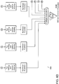
- FIG. 7 schematically illustrates an envelope detector core structure 700 that is used for envelope detection in the various RMS and envelope detectors in accordance with one or more embodiments.
- the detector comprises a plurality of bipolar triple-tail cells (indicated in the FIG. 7 example as the 1st stage and 2nd stage).
- Each triple-tail cell includes three emitter-coupled npn bipolar transistors (Q1, Q2, Q3 in the first stage, Q4, Q5, Q6 in the second stage) and a current source coupled to the common-emitter generating a tail-current Idc1, Idc2.
- the transistors Q1 and Q3 of the first stage form a differential pair with emitter areas equal to each other (Ae).
- the transistors Q4 and Q6 of the second stage form a differential pair with emitter areas equal to each other (Ce).
- the transistors Q2 and Q5 may have different emitter areas (Be and De, respectively) than their respective differential pairs.
- the ratios B/A or D/C may be unity, or may be greater or less than unity.
- the collectors of the transistors Q1 and Q3 of the first stage are coupled together forming the output terminal of an envelope detector core stage, while the collector of Q2 is coupled to an AC ground.
- the collectors of the transistors Q4 and Q6 of the second stage are coupled together forming the output terminal of an envelope detector core stage, while the collector of Q5 is coupled to an AC ground.
- the bases of the center transistors Q2 and Q5 receive only the dc component "DC”.
- the center transistors may receive a parasitic RF component.
- the type-2 stage uses two emitter degeneration resistors R2 that are coupled between the emitter of the differential pair transistors Q4, Q6 and the common emitter node (which is coupled to the current source).
- the degeneration resistors linearize the output-input transfer curve of the stage for mid and high level input signals when used with a proper D/C ratio (preferably D/C >> 1 in the current embodiment).
- the type-1 stage uses a single emitter degeneration resistor R1 that is coupled between the emitter of the center transistor Q2 and the common emitter node.
- the degeneration resistor linearizes the output-input transfer curve of the combined structure (including both type-1 and type-2 stages) for lower input signal levels with a proper B/A ratio (preferably B/A ⁇ 1 in the current embodiment).
- emitter degeneration resistors R1 and R2 expand the linear operating input voltage range of the envelope detector core.
- FIG. 8 shows an example of the output-input characteristics of the type-1 and type-2 stages as well as the combined structure. As shown, the type-2 stage provides approximately linear characteristics for input signal levels of Vinp > 150mV, while the combined structure provides approximately linear characteristics for input signal levels of Vinp > 50mV, resulting in a significant improvement in the dynamic range.
- Type-2 stages can be provided in parallel with different degeneration values and D/C ratios to further increase the dynamic range for higher signal levels.
Landscapes
- Physics & Mathematics (AREA)
- Engineering & Computer Science (AREA)
- General Physics & Mathematics (AREA)
- Electromagnetism (AREA)
- Computer Networks & Wireless Communication (AREA)
- Signal Processing (AREA)
- Power Engineering (AREA)
- Amplifiers (AREA)
- Measurement Of Current Or Voltage (AREA)
Description
- This application claims priority from
U.S. Provisional Patent Application Serial No. 61/383,820, filed on September 17, 2010 - The present application relates generally to root mean square (RMS) detectors and envelope detectors.
- There are many applications in which it is desirable to measure the average power level of a radio frequency (RF) signal. For example, power measurement and control of RF signals in both the transmitting and receiving chains of modern wireless communications systems, such as cellular telephone networks, may be essential. To efficiently use the available bandwidth, the transmitted signals in these systems are modulated using complex modulation schemes such as Code Division Multiple Access (CDMA), Wideband Code Division Multiple Access (WCDMA), or Worldwide Interoperability for Microwave Access (WiMAX). These complex modulated signals have a time varying crest factor, which is defined as the peak to average power ratio of the signal. Intolerable errors can result if conventional power detectors using diode detection or successive amplification are used to measure the signal power.
- Another challenge in modern wireless communication systems is improving the power efficiency of power amplifiers used in the transmit chain. Efficient use of power amplifiers is important in mobile communications systems. Improved power efficiency can provide significant benefits including lower overall operating costs. Improving the power efficiency of power amplifiers is especially difficult when high-crest factor signals (having a peak power of 10+dB more than the average power) are transmitted since the transmitter should be put in a deep back-off mode (very low average power output) to handle the linearity requirements for peak signal levels. To improve power efficiency, it is known to apply envelope tracking to the power amplifier input signal, and to use the detected envelope to vary the amplifier operation. For supplying power to the power amplifier, a variable power supply is utilized in an envelope tracking system. The input signal envelope power levels are monitored using an envelope detector, and the power that is supplied to the power amplifier is varied based on the monitored envelope levels. In particular, the supply voltage supplied to the power amplifier is varied so as to be just sufficient to reproduce the power level required by the amplifier at a given instant of time. Accordingly, at low envelope power levels, a low supply voltage is provided to the amplifier, and the full supply voltage is only provided when the maximum output envelope power is required, i.e., at the output power peaks.
- RMS power detectors can precisely measure RF power independent of the modulation type (signal shape or crest-factor). Accurate RMS calculation of these complex modulation schemes requires long integration times to include the time-varying envelope in the measurement. Thus, commercially available RMS power detectors are generally not capable of providing the envelope level of the modulated signals.
- Therefore, for transmitter systems, it is desirable to have a power detector that provides both average power information and input voltage envelope information.
-
US 2010/0097143 A1 describes an RF detector configured to provide two outputs, one being a function of the true RMS power level of an RF input signal, and the other being a function of the instantaneous/peak power of the RF input signal, normalized to the average power level. The RF detector includes a variable gain detection subsystem including a single detector or detector array that provides a representation of the power level of the RF input signal. The detector or detector array is common to both the RMS power detection channel and the instantaneous/peak power detection channel of the RF detector. A method of RF detection includes providing representations of the RF input signal at different gain levels, selecting one or more of the representations, and averaging the selected signals. The gain levels of the selected representations is adjusted to provide information about the average power level of the RF input signal. - "Analog Devices: Preliminary Technical Data ADL5502: 800 MHz to 3800 MHz Crest Factor Detector" describes a mean-responding power detector in combination with an envelope detector to accurately determine the crest factor of a modulated signal.
- A power detector in accordance with a first embodiment of the disclosure is defined in
claim 1 and a power detector in accordance with a second embodiment of the disclosure is defined inclaim 2. A method of detecting power of an RF signal in accordance with the first embodiment of the disclosure is defined inclaim 8 and a method of detecting power of an RF signal in accordance with the second embodiment of the disclosure is defined inclaim 9. - The power detector may include a gain or attenuation element. The logarithmic RMS detector receives an RF input signal and detects the average power level of the RF input signal. The gain or attenuation element also receives the RF input signal and generates an amplified or attenuated version of the RF input signal. The linear envelope detector receives the amplified or attenuated version of the RF input signal and detects the voltage envelope of the RF input signal, wherein the gain or attenuation element can generate a selected amplified or attenuated version of the RF input signal to shift the operating range of the envelope detector to higher or lower power levels.
- The method of detecting power of an RF input signal may further comprise generating an amplified or attenuated version of the RF input signal; and detecting the voltage envelope of the RF input signal using the amplified or attenuated version of the RF input signal, wherein the amplified or attenuated version of the RF input signal is selectively generated to shift the operating range of the envelope detector to higher or lower power levels.
- The logarithmic RMS detector may include a series of gain or attenuation stages that progressively amplify or attenuate the RF input signal. The logarithmic RMS detector may also include a plurality of mean square detectors, at least some of which are driven with amplified or attenuated versions of the RF input signal from the series of gain or attenuation stages. The envelope detector may be selectively coupled to an RF input for receiving the RF input signal or to one of a plurality of gain or attenuation taps of the series of gain or attenuation stages of the RMS detector for receiving an amplified or attenuated version of the RF input signal to shift the operating range of the envelope detector.
- The method of detecting power may comprise the steps of progressively amplifying or attenuating an RF input signal to generate a plurality of amplified or attenuated versions of the RF input signal; detecting the average power level of the RF input signal using a logarithmic RMS detector including a plurality of mean square detectors, at least some of which are driven with the plurality of amplified or attenuated versions of the RF input signal; and detecting the voltage envelope of the RF input signal using a linear envelope detector receiving the RF input signal or one of the plurality of amplified or attenuated versions of the RF input signal selected to shift the operating range of the envelope detector.
- The linear envelope detector for detecting the voltage envelope of an RF input signal may comprise a plurality of bipolar triple-tail cells. Each triple-tail cell includes two differential transistors and a center transistor. In each triple-tail cell, each of the transistors has a common emitter node coupled to a current source generating a tail-current. The collectors of the differential transistors of each triple-tail cell are coupled together to form an output of the envelope detector. In each triple-tail cell, a differential input voltage is applied between the bases of the differential transistors with a DC voltage component, and an input voltage with only a DC voltage component is applied to the base of the center transistor.
- The linear envelope detector for detecting the voltage envelope of an RF input signal may comprise a plurality of bipolar triple-tail cells. Each triple-tail cell includes two differential transistors and a center transistor. In each triple-tail cell, each of the transistors has a common emitter node coupled to a current source generating a tail-current. The collectors of the differential transistors of each triple-tail cell are coupled together to form an output of the envelope detector. In each triple-tail cell, a first signal is applied between the bases of a first one of the two differential transistors and the center transistor and a second signal is applied between the bases of a second one of the differential transistors and the center transistor, wherein the first and the second signals form a differential signal.
- The linear envelope detector for detecting the voltage envelope of an RF input signal may comprise a plurality of bipolar triple-tail cells. Each triple-tail cell includes two differential transistors and a center transistor. In each triple-tail cell, each of the transistors has a common emitter node coupled to a current source generating a tail-current. The collectors of the differential transistors of each triple-tail cell are coupled together to form an output of the envelope detector. In each triple-tail cell, a differential input voltage is applied between the bases of the differential transistors with a DC voltage component, and an input voltage with a parasitic RF component is applied to the base of the center transistor.
- Various embodiments of the invention are provided in the following detailed description. As will be realized, the invention is capable of other and different embodiments, and its several details may be capable of modifications in various respects, all without departing from the invention. Accordingly, the drawings and description are to be regarded as illustrative in nature and not in a restrictive or limiting sense, with the scope of the application being indicated in the claims.
-
-
FIG. 1 is a schematic diagram of a prior art RMS and envelope detector. -
FIG. 2 is a schematic diagram of another prior art RMS and envelope detector. -
FIG. 3 is a schematic diagram of another prior art RMS and envelope detector. -
FIG. 4 is a schematic diagram of an RMS and envelope detector in accordance with one or more embodiments. -
FIG. 5 is a schematic diagram of an RMS and envelope detector in accordance with one or more further embodiments. -
FIG. 6 is a schematic diagram of an RMS and envelope detector in accordance with one or more further embodiments. -
FIG. 7 is a schematic diagram of an envelope detector core structure in accordance with one or more embodiments. -
FIG. 8 is a graph illustrating exemplary output-input characteristics of triple-tail cells. - Like or identical reference numbers are used to identify common or similar elements.
-
FIG. 1 is a schematic block diagram illustrating a prior art RMS andenvelope detector 100, which uses twoseparate chips RMS detector 102 and theenvelope detector 104. Discrete implementation of RMS and envelope detection also generally requires a larger board area to accommodate both chips and required interface circuitry such as an input coupler. -
FIG. 2 is a block diagram of a prior art singlepackage power detector 200 providing both the envelope and RMS power information. The RF input is provided to separate RMS detector and envelope detector blocks 202, 204 through aDC decoupling capacitor 206. TheRMS detector 202 is of linear type (Vout ∼ Sqrt(Mean(Vin2))), meaning that the output voltage changes exponentially for dB changes in the input power. For these type of detectors, especially at lower power levels (e.g., less than -10dBm), the detected voltage level is very sensitive to mismatches and environmental variations such as temperature, and this limits the minimum detectable signal levels to about -15dBm. Theenvelope detector 204 also has similar limitations, resulting in a detectable input power range of about -15dBm to 10dBm for both detectors. Although the simplicity of this approach may result in a smaller package size and lower power dissipation, theprior art detector 200 is only useful for a limited level of input signals. Also, a linear RMS detector output is usually not preferable in power control applications because of larger reading errors for low input power levels. -
FIG. 3 illustrates another priorart power detector 300 providing both envelope and RMS power information. Thedetector 300 uses a servo feedback type RMS detection architecture for high dynamic range operation. The detector can detect signal levels down to -70dBm, giving it a significantly higher dynamic range than linear type RMS detectors. - The envelope detection channel receives its input from an internal point of the servo feedback loop and this buffered internal point provides the power envelope of the input signal that is normalized to the average power level of the input signal. This architecture provides a high dynamic range for both RMS and envelope detection (the envelope detection dynamic range is equivalent to the RMS detection range -- more than 70dB possible) with exceptional repeatability (over temperature and process variations) as well as exceptional matching between the RMS power reading and power envelope reading. Most envelope tracking applications, however, require the envelope detector to track the voltage envelope of the input signal instead of the power envelope, and this type of architecture may accordingly not be suitable because it tracks the power envelope.
-
FIG. 4 is a block diagram illustrating a singlepackage power detector 400 providing both envelope and RMS power information in accordance with one or more embodiments of the invention. An RF input is coupled to separate RMS detector and envelope detector blocks 402, 404, which process the input signal separately. TheRMS detector 402 and theenvelope detector 404 are provided in asingle package 406 and preferably on a single die. - The
RMS detector 402 is a logarithmic type (Vout ∼ Log(Mean(Vin2))) RMS detector, in which the output voltage changes linearly for dB changes in the input power. Logarithmic RMS detectors provide significantly larger input dynamic ranges compared to linear RMS detector types. They are especially useful for power/gain control applications because they have linear-in-dB characteristics and provide higher accuracy at low power levels (e.g., detection down to -70dBm is possible). - With direct coupling of the RF input signal to the envelope detector, the envelope detection dynamic range is lower (limited to about -15dBm at low power end and +10dBm at the top end).
-
FIG. 5 is a block diagram of an RMS andenvelope detector 500 in accordance with one or more further embodiments. Thedetector 500 is similar to thedetector 400 shown inFIG. 4 , and further includes a gain/attenuation block 502. In theFIG. 5 embodiment, the RF input is coupled to the gain/attenuation block 502 to provide amplification/attenuation to the input signal. The output of the gain/attenuation block is coupled to theenvelope detector 404. The operating range of the envelope detector 404 (the range of input signals to which the envelope detector accurately responds) can be shifted to lower or higher power levels. For example, for a gain of 20dB in the gain/attenuation block 502, theenvelope detector 404 can detect RF signals from about -35dBm to -10dBm. -
FIG. 6 is a block diagram of an RMS andenvelope detector 600 in accordance with one or more further embodiments of the invention. In this embodiment, anenvelope detector core 602 is coupled to one of a plurality of gain/attenuation taps 604 of anRMS detector 606. - In this embodiment, the
RMS detector 606 includes a plurality of mean square detectors, some of which are driven with amplified or attenuated versions of an RF input signal to obtain a wider range of mean square power detection than a single mean square detector. The amplified or attenuated versions of the RF input signal are obtained by using a series of gain or attenuation operations that progressively amplify or attenuate the RF inputsignal using amplifiers 608 orattenuators 610. - The operating range of the envelope detector 602 (the range of input signals that the envelope detector accurately responds to) can be shifted to lower or higher power levels similar to the
FIG. 5 embodiment. However, in theFIG. 6 embodiment, there is no need for additional amplification/attenuation because the amplified/attenuated taps ofRMS detector 606 can be used to supply the needed gain/attenuation. For gain/attenuation separation of 7dB, the envelope detector operation range can be shifted in 7dB steps. For example, if theenvelope detector 602 is coupled to the 3rd gain tap of the architecture (21dB gain from input), theenvelope detector 602 can detect RF signals from -36dBm to -11dBm assuming that the envelope detector has 25dB detection range. -
FIG. 7 schematically illustrates an envelopedetector core structure 700 that is used for envelope detection in the various RMS and envelope detectors in accordance with one or more embodiments. The detector comprises a plurality of bipolar triple-tail cells (indicated in theFIG. 7 example as the 1st stage and 2nd stage). Each triple-tail cell includes three emitter-coupled npn bipolar transistors (Q1, Q2, Q3 in the first stage, Q4, Q5, Q6 in the second stage) and a current source coupled to the common-emitter generating a tail-current Idc1, Idc2. The transistors Q1 and Q3 of the first stage form a differential pair with emitter areas equal to each other (Ae). The transistors Q4 and Q6 of the second stage form a differential pair with emitter areas equal to each other (Ce). The transistors Q2 and Q5 may have different emitter areas (Be and De, respectively) than their respective differential pairs. The ratios B/A or D/C may be unity, or may be greater or less than unity. The collectors of the transistors Q1 and Q3 of the first stage are coupled together forming the output terminal of an envelope detector core stage, while the collector of Q2 is coupled to an AC ground. Similarly, the collectors of the transistors Q4 and Q6 of the second stage are coupled together forming the output terminal of an envelope detector core stage, while the collector of Q5 is coupled to an AC ground. - In this configuration, a differential input voltage Vinp=INP-INN is applied between the bases of the transistors Q1, Q3 and Q4, Q6 with a dc voltage component denoted as "DC". The bases of the center transistors Q2 and Q5 receive only the dc component "DC". In an alternative embodiment, the center transistors may receive a parasitic RF component. In a further embodiment, one of the transistors in the differential pair Q1, Q3 or Q4, Q6 can receive a DC voltage at its base and the other two transistors (one of Q1, Q3 and also Q2, or one of Q4, Q6 and also Q5) can receive input signals that effectively generate a differential voltage across base inputs of Q1-Q2=Q4-Q5 (= Vinp/2) and Q3-Q2=Q6-Q5 (= -Vinp/2).
- In the embodiment illustrated in
FIG. 7 , two types of triple-tail cells are used in the envelope detector core (1st stage=type-1, 2nd stage=type-2). The type-2 stage uses two emitter degeneration resistors R2 that are coupled between the emitter of the differential pair transistors Q4, Q6 and the common emitter node (which is coupled to the current source). The degeneration resistors linearize the output-input transfer curve of the stage for mid and high level input signals when used with a proper D/C ratio (preferably D/C >> 1 in the current embodiment). The type-1 stage, on the other hand, uses a single emitter degeneration resistor R1 that is coupled between the emitter of the center transistor Q2 and the common emitter node. The degeneration resistor linearizes the output-input transfer curve of the combined structure (including both type-1 and type-2 stages) for lower input signal levels with a proper B/A ratio (preferably B/A < 1 in the current embodiment). In summary, emitter degeneration resistors R1 and R2 expand the linear operating input voltage range of the envelope detector core.FIG. 8 shows an example of the output-input characteristics of the type-1 and type-2 stages as well as the combined structure. As shown, the type-2 stage provides approximately linear characteristics for input signal levels of Vinp > 150mV, while the combined structure provides approximately linear characteristics for input signal levels of Vinp > 50mV, resulting in a significant improvement in the dynamic range. - It should be noted that additional Type-2 stages can be provided in parallel with different degeneration values and D/C ratios to further increase the dynamic range for higher signal levels.
Claims (13)
- A power detector (400, 500, 600), comprising:a logarithmic RMS detector (402, 606) configured to:receive an RF input signal (RFin); anddetect the average power level of the RF input signal; anda linear envelope detector (404, 602), configured to:
detect the voltage envelope of the RF input signal;wherein the linear envelope detector comprises:
a plurality of bipolar triple-tail cells, each triple-tail cell including two differential transistors (Q1 and Q3, Q4 and Q6) and a center transistor (Q2, Q5), andwherein in each triple-tail cell, each of the transistors has a common emitter node coupled to a current source configured to generate a tail-current (Idc1, Idc2), each triple-tail cell being configured to receive a differential input voltage between the bases of the differential transistors with a DC voltage component, and either a) an input voltage with a DC voltage component, or b) a parasitic RF component, on the base of the center transistor,wherein the collectors of the differential transistors of the triple-tail cells are all coupled together to an output terminal of the linear envelope detector; andwherein the logarithmic RMS detector and the envelope detector are integrated in a single package. - A power detector (400, 500, 600), comprising:a logarithmic RMS detector (402, 606) configured to:receive an RF input signal (RFin); anddetect the average power level of the RF input signal; anda linear envelope detector (404, 602), configured to:
detect the voltage envelope of the RF input signal;wherein the linear envelope detector comprises:
a plurality of bipolar triple-tail cells, each triple-tail cell including two differential transistors (Q1 and Q3, Q4 and Q6) and a center transistor (Q2, Q5), andwherein in each triple-tail cell, each of the transistors has a common emitter node coupled to a current source configured to generate a tail-current (Idc1, Idc2), each triple-tail cell being configured to receive a first signal between the bases of a first one of the two differential transistors and the center transistor and a second signal between the bases of a second one of the differential transistors and the center transistor, wherein the first and the second signals form a differential signal;wherein the collectors of the differential transistors of the triple-tail cells are all coupled together to an output terminal of the linear envelope detector; andwherein the logarithmic RMS detector and the envelope detector are integrated in a single package. - The power detector of claim 1 or claim 2, wherein the RMS detector and the envelope detector are integrated on a single die.
- The power detector of any of claims 1 to 3, further comprising a gain or attenuation element (502) configured to:receive the RF input signal; andgenerate an amplified or attenuated version of the RF input signal; andwherein the linear envelope detector is configured to receive the amplified or attenuated version of the RF input signal and detect the voltage envelope of the RF input signal, wherein the gain or attenuation element is configured to generate a selected amplified or attenuated version of the RF input signal to shift the operating range of the envelope detector to higher or lower power levels.
- The power detector of any of claims 1 to 3, wherein the logarithmic RMS detector includes a series of gain or attenuation stages (608, 610) configured to progressively amplify or attenuate the RF input signal, and the logarithmic RMS detector also includes a plurality of mean square detectors, at least some of which are driven with amplified or attenuated versions of the RF input signal from the series of gain or attenuation stages; and
wherein the linear envelope detector is selectively coupled to an RF input for receiving the RF input signal or to one of a plurality of gain or attenuation taps (604) of the series of gain or attenuation stages of the RMS detector for receiving an amplified or attenuated version of the RF input signal to shift the operating range of the envelope detector. - The power detector of any preceding claim, wherein at least one of the triple-tail cells further comprise an emitter degeneration resistor (R2) coupled between the emitter of each of the two differential transistors and the common emitter node.
- The power detector of claim 6, wherein at least one of the triple-tail cells different from triple-tail cells with an emitter degeneration resistor on the differential transistors further comprises an emitter degeneration resistor (R1) coupled between the emitter of the center transistor and the common emitter node.
- A method of detecting power of an RF input signal (RFin), comprising the steps of:detecting the average power level of the RF input signal using a logarithmic RMS detector (402, 606);detecting the voltage envelope of the RF input signal using a linear envelope detector (404, 602);wherein the linear envelope detector comprises a plurality of bipolar triple-tail cells, each triple-tail cell including two differential transistors (Q1 and Q3, Q4 and Q6) and a center transistor (Q2, Q5), andwherein in each triple-tail cell, each of the transistors has a common emitter node coupled to a current source generating a tail-current (Idc1, Idc2), a differential input voltage is applied between the bases of the differential transistors with a DC voltage component, and either a) an input voltage with a DC voltage component, or b) a parasitic RF component, is applied to the base of the center transistor, andwherein the collectors of the differential transistors of the triple-tail cells are all coupled together to an output terminal of the linear envelope detector, andwherein the logarithmic RMS detector and the envelope detector are integrated in a single package.
- A method of detecting power of an RF input signal (RFin), comprising the steps of:detecting the average power level of the RF input signal using a logarithmic RMS detector (402, 606);detecting the voltage envelope of the RF input signal using a linear envelope detector (404, 602);wherein the linear envelope detector comprises a plurality of bipolar triple-tail cells, each triple-tail cell including two differential transistors (Q1 and Q3, Q4 and Q6) and a center transistor (Q2, Q5), andwherein in each triple-tail cell, each of the transistors has a common emitter node coupled to a current source generating a tail-current (Idc1, Idc2), a first signal is applied between the bases of a first one of the two differential transistors and the center transistor and a second signal is applied between the bases of a second one of the differential transistors and the center transistor, wherein the first and the second signals form a differential signal, andwherein the collectors of the differential transistors of the triple-tail cells are all coupled together to an output terminal of the linear envelope detector, andwherein the logarithmic RMS detector and the envelope detector are integrated in a single package.
- The method of claim 8 or claim 9 wherein the RMS detector and the envelope detector are integrated on a single die.
- A method of any of claims 8 to 10, further comprising generating an amplified or attenuated version of the RF input signal; and
wherein detecting the voltage envelope of the RF input signal comprises using the amplified or attenuated version of the RF input signal, wherein the amplified or attenuated version of the RF input signal is selectively generated to shift the operating range of the envelope detector to higher or lower power levels. - The method of claim 11, wherein a gain or attenuation element (502) is used for generating the amplified or attenuated version of the RF input signal, and wherein a linear envelope detector is used for detecting the voltage envelope of the RF input signal.
- A method of any of claims 8 to 10, further comprising progressively amplifying or attenuating an RF input signal to generate a plurality of amplified or attenuated versions of the RF input signal;
wherein detecting the average power level of the RF input signal comprises using a logarithmic RMS detector including a plurality of mean square detectors, at least some of which are driven with the plurality of amplified or attenuated versions of the RF input signal; and
wherein detecting the voltage envelope of the RF input signal using a linear envelope detector comprises receiving the RF input signal or one of the plurality of amplified or attenuated versions of the RF input signal selected to shift the operating range of the envelope detector.
Applications Claiming Priority (1)
| Application Number | Priority Date | Filing Date | Title |
|---|---|---|---|
| US38382010P | 2010-09-17 | 2010-09-17 |
Publications (3)
| Publication Number | Publication Date |
|---|---|
| EP2437073A2 EP2437073A2 (en) | 2012-04-04 |
| EP2437073A3 EP2437073A3 (en) | 2016-07-20 |
| EP2437073B1 true EP2437073B1 (en) | 2020-03-25 |
Family
ID=45373674
Family Applications (1)
| Application Number | Title | Priority Date | Filing Date |
|---|---|---|---|
| EP11181290.5A Active EP2437073B1 (en) | 2010-09-17 | 2011-09-14 | RMS and envelope detector |
Country Status (4)
| Country | Link |
|---|---|
| US (2) | US9625498B2 (en) |
| EP (1) | EP2437073B1 (en) |
| CN (1) | CN102435835B (en) |
| TW (1) | TWI532999B (en) |
Families Citing this family (11)
| Publication number | Priority date | Publication date | Assignee | Title |
|---|---|---|---|---|
| TWI472776B (en) * | 2009-11-23 | 2015-02-11 | Hittite Microwave Corp | Logarithmic mean-square power detector |
| US9625498B2 (en) | 2010-09-17 | 2017-04-18 | Hittite Microwave Llc | RMS and envelope detector |
| US9678920B1 (en) * | 2012-04-04 | 2017-06-13 | Marvell International Ltd. | Self-calibration and compensation of detector offset in GSM transceivers power control loop |
| US9178476B2 (en) * | 2012-09-26 | 2015-11-03 | Broadcom Corporation | Envelope detector with enhanced linear range |
| US8952742B2 (en) * | 2012-10-31 | 2015-02-10 | Marvell World Trade Ltd. | Highly accurate true RMS power detector for cellular applications |
| US8744379B1 (en) * | 2012-12-31 | 2014-06-03 | Futurewei Technologies, Inc. | Temperature independent CMOS radio frequency power detector |
| US9590740B1 (en) * | 2014-10-22 | 2017-03-07 | The United States Of America, As Represented By The Secretary Of The Navy | Method and system for robust symmetrical number system photonic direction finding |
| US10361744B1 (en) * | 2018-03-05 | 2019-07-23 | Qorvo Us, Inc. | Transceiver circuit and related radio frequency circuit |
| US10886938B2 (en) * | 2018-09-05 | 2021-01-05 | Atmosic Technologies Inc. | Active analog front-end |
| IT202100007844A1 (en) * | 2021-03-30 | 2022-09-30 | St Microelectronics Srl | MATCHING ENVELOPE DETECTOR CIRCUIT, RECEIVER CIRCUIT AND GALVANIC ISOLATOR DEVICE |
| US11349512B1 (en) * | 2021-04-23 | 2022-05-31 | Analog Devices International Unlimited Company | Logarithmic power detector with noise compensation |
Family Cites Families (50)
| Publication number | Priority date | Publication date | Assignee | Title |
|---|---|---|---|---|
| US3517216A (en) | 1968-01-04 | 1970-06-23 | Bendix Corp | Means for generating a video constant false alarm rate signal at video frequencies |
| US3992584A (en) | 1975-05-09 | 1976-11-16 | Dugan Daniel W | Automatic microphone mixer |
| US4047235A (en) | 1976-08-13 | 1977-09-06 | General Electric Company | Current limit and overcurrent cut off system |
| US4156848A (en) | 1977-05-02 | 1979-05-29 | Motorola, Inc. | High dynamic range detector for indicating the quieting level of an FM receiver |
| US4758793A (en) | 1987-02-10 | 1988-07-19 | Raytheon Company | Detector log video amplifier |
| US4873484A (en) | 1987-09-03 | 1989-10-10 | Lucas Weinschel, Inc. | Extended range composite head power sensor with three circuit branches having a common node |
| US4823807A (en) * | 1988-02-11 | 1989-04-25 | Board Of Regents, Univ. Of Texas System | Device for non-invasive diagnosis and monitoring of articular and periarticular pathology |
| US4990803A (en) | 1989-03-27 | 1991-02-05 | Analog Devices, Inc. | Logarithmic amplifier |
| GB2232841B (en) | 1989-05-19 | 1994-01-26 | Quantel Ltd | An amplification circuit with temperature compensation |
| US5126686A (en) | 1989-08-15 | 1992-06-30 | Astec International, Ltd. | RF amplifier system having multiple selectable power output levels |
| GB2246888B (en) | 1990-07-04 | 1994-01-19 | Thorn Emi Electronics Ltd | Calculating apparatus |
| US5077541A (en) | 1990-08-14 | 1991-12-31 | Analog Devices, Inc. | Variable-gain amplifier controlled by an analog signal and having a large dynamic range |
| EP0517305B1 (en) | 1991-06-03 | 1995-11-22 | Koninklijke Philips Electronics N.V. | Logarithmic amplifier and detector |
| US5220276A (en) | 1991-06-11 | 1993-06-15 | Keithley Corporation | Crest factor measurement device |
| US5298811A (en) | 1992-08-03 | 1994-03-29 | Analog Devices, Inc. | Synchronous logarithmic amplifier |
| US5473244A (en) | 1992-09-17 | 1995-12-05 | Libove; Joel M. | Apparatus for measuring voltages and currents using non-contacting sensors |
| US5402451A (en) | 1993-01-11 | 1995-03-28 | Hughes Aircraft Company | Digital post-detection FM spatial diversity combination circuit |
| US5450029A (en) | 1993-06-25 | 1995-09-12 | At&T Corp. | Circuit for estimating a peak or RMS value of a sinusoidal voltage waveform |
| US5432478A (en) | 1994-01-21 | 1995-07-11 | Analog Devices, Inc. | Linear interpolation circuit |
| AU691554B2 (en) * | 1994-03-09 | 1998-05-21 | Nec Corporation | Analog multiplier using multitail cell |
| JP2606599B2 (en) * | 1994-09-09 | 1997-05-07 | 日本電気株式会社 | Logarithmic amplifier circuit |
| US5608409A (en) | 1995-03-28 | 1997-03-04 | Rilling; Kenneth F. | Adaptive array with automatic loop gain control |
| US5815039A (en) * | 1995-07-21 | 1998-09-29 | Nec Corporation | Low-voltage bipolar OTA having a linearity in transconductance over a wide input voltage range |
| US5668750A (en) | 1995-07-28 | 1997-09-16 | Nec Corporation | Bipolar multiplier with wide input voltage range using multitail cell |
| GB2305564A (en) | 1995-09-19 | 1997-04-09 | Nec Corp | Bipolar operational transconductance amplifier |
| JPH09148857A (en) | 1995-09-19 | 1997-06-06 | Nec Corp | Bipolar ota |
| US5790943A (en) | 1995-10-06 | 1998-08-04 | Philips Electronics North America Corporation | Dynamic range extension of a log amplifier with temperature and process compensation |
| JPH09219630A (en) * | 1995-12-08 | 1997-08-19 | Nec Corp | Differential circuit |
| US5684431A (en) | 1995-12-13 | 1997-11-04 | Analog Devices | Differential-input single-supply variable gain amplifier having linear-in-dB gain control |
| US5724003A (en) | 1995-12-29 | 1998-03-03 | Maxim Integrated Products, Inc. | Methods and apparatus for signal amplitude control systems |
| US6098463A (en) | 1997-02-18 | 2000-08-08 | Etymotic Research, Inc. | Method and apparatus for measurement of wide dynamic range signals |
| US5925095A (en) | 1997-05-12 | 1999-07-20 | International Business Machines Corporation | Method and a computer program product for client/server computing with support for both recoverable and non-recoverable clients |
| JPH11250168A (en) | 1998-03-04 | 1999-09-17 | Nec Corp | Square number calculation circuit, composite deferential amplifier circuit and multiplier using these circuits |
| US6291984B1 (en) | 1999-06-18 | 2001-09-18 | Anritsu Company | Dual mode diode power sensor with square law and linear operating regions |
| US6437630B1 (en) | 1999-12-28 | 2002-08-20 | Analog Devices, Inc. | RMS-DC converter having gain stages with variable weighting coefficients |
| EP1184671B1 (en) | 2000-08-24 | 2006-12-06 | Sony Deutschland GmbH | Power detector using FET transistor |
| CN2549652Y (en) | 2002-03-29 | 2003-05-07 | 深圳市中兴通讯股份有限公司上海第二研究所 | Self gain-control linear power amplifier |
| US7242779B2 (en) * | 2002-05-30 | 2007-07-10 | Peavey Electronics Corporation | Methods and apparatus for sub-harmonic generation, stereo expansion and distortion |
| DE602004010237T2 (en) | 2003-02-14 | 2008-10-02 | Analog Devices Inc., Norwood | SYSTEM AND METHOD FOR REDUCING THE TRANSMISSION FUNCTIONAL WAVE IN A LOGORITHMIC RMS-TO-DC CONVERTER |
| US7123086B2 (en) * | 2003-05-07 | 2006-10-17 | Powerwave Technologies, Inc. | Feed forward amplifier employing positive feedback pilot generation |
| US6963243B2 (en) * | 2003-10-22 | 2005-11-08 | Andrew Corporation | Amplifier pre-distortion processing based on composite look-up tables |
| EP1557680A1 (en) | 2004-01-26 | 2005-07-27 | STMicroelectronics S.r.l. | Device for detecting the power of a radio frequency signal |
| US20050228644A1 (en) | 2004-03-31 | 2005-10-13 | Bea Systems, Inc. | Generic user interface testing framework with rules-based wizard |
| US7440733B2 (en) * | 2004-04-09 | 2008-10-21 | Powerwave Technologies, Inc. | Constant gain nonlinear envelope tracking high efficiency linear amplifier |
| US7355478B2 (en) * | 2006-06-30 | 2008-04-08 | Andrew Corporation | RF amplifier with pulse detection and bias control |
| TW200805029A (en) * | 2006-07-12 | 2008-01-16 | Beyond Innovation Tech Co Ltd | Voltage control current source and frequency scanner using the same |
| WO2008143895A2 (en) | 2007-05-14 | 2008-11-27 | Hittite Microwave Corporation | Rf detector with crest factor measurement |
| US7777552B1 (en) * | 2008-04-29 | 2010-08-17 | Analog Devices, Inc. | Logarithmic amplifier with RMS post-processing |
| TWI472776B (en) | 2009-11-23 | 2015-02-11 | Hittite Microwave Corp | Logarithmic mean-square power detector |
| US9625498B2 (en) | 2010-09-17 | 2017-04-18 | Hittite Microwave Llc | RMS and envelope detector |
-
2011
- 2011-09-06 US US13/225,904 patent/US9625498B2/en active Active
- 2011-09-14 EP EP11181290.5A patent/EP2437073B1/en active Active
- 2011-09-15 TW TW100133180A patent/TWI532999B/en active
- 2011-09-16 CN CN201110275214.6A patent/CN102435835B/en active Active
-
2017
- 2017-03-16 US US15/461,233 patent/US10012679B2/en active Active
Non-Patent Citations (1)
| Title |
|---|
| None * |
Also Published As
| Publication number | Publication date |
|---|---|
| US10012679B2 (en) | 2018-07-03 |
| EP2437073A2 (en) | 2012-04-04 |
| TWI532999B (en) | 2016-05-11 |
| CN102435835A (en) | 2012-05-02 |
| TW201224465A (en) | 2012-06-16 |
| CN102435835B (en) | 2016-05-04 |
| US20120071125A1 (en) | 2012-03-22 |
| US20170248637A1 (en) | 2017-08-31 |
| US9625498B2 (en) | 2017-04-18 |
| EP2437073A3 (en) | 2016-07-20 |
Similar Documents
| Publication | Publication Date | Title |
|---|---|---|
| US10012679B2 (en) | Envelope detector with bipolar triple-tail cells | |
| US5880631A (en) | High dynamic range variable gain amplifier | |
| US6744319B2 (en) | Exponential function generator embodied by using a CMOS process and variable gain amplifier employing the same | |
| CN102753981B (en) | Logarithmic mean-square power detector | |
| Holdenried et al. | A DC-4-GHz true logarithmic amplifier: theory and implementation | |
| US7109796B2 (en) | Amplifying circuit with adjustable amplification and transmitter system comprising such an amplifying circuit | |
| CN113572433B (en) | RF differential amplifier circuit and RF module | |
| US20120034895A1 (en) | Circuit and Method for Peak Detection with Hysteresis | |
| CN114189292B (en) | Power detection circuit, power amplifier module and radio frequency front end architecture | |
| KR100572187B1 (en) | High dynamic range variable gain amplifier | |
| US20240405737A1 (en) | Wide-band logarithmic power detectors | |
| CN111049487A (en) | Automatic gain control circuit and control method | |
| US5461342A (en) | Wide bandwidth, phase-stable amplifier circuit and method | |
| CN103095232A (en) | Dual slope logarithmic amplifier circuit structure | |
| CN213990615U (en) | A power amplifier module and circuit | |
| US6750713B1 (en) | Variable gain amplifier | |
| CN116582144A (en) | A power adaptive link distribution front-end receiving component | |
| CN210405325U (en) | Power detector | |
| CN101098125B (en) | Rf amplifier with pulse detection and bias control | |
| CN117118375B (en) | A continuous dB linear wideband variable gain amplifier | |
| CN215575633U (en) | Miniature meteorological radar calibration circuit | |
| CN201846312U (en) | Broad frequency power amplifier | |
| Mao et al. | An Improved Bidirectional Gain-Configurable AGC Circuit at Transmitter | |
| CN115913417A (en) | A device and method for improving the detection range and accuracy of a radio frequency power detector | |
| JPS5875906A (en) | High frequency linear amplifier |
Legal Events
| Date | Code | Title | Description |
|---|---|---|---|
| PUAI | Public reference made under article 153(3) epc to a published international application that has entered the european phase |
Free format text: ORIGINAL CODE: 0009012 |
|
| AK | Designated contracting states |
Kind code of ref document: A2 Designated state(s): AL AT BE BG CH CY CZ DE DK EE ES FI FR GB GR HR HU IE IS IT LI LT LU LV MC MK MT NL NO PL PT RO RS SE SI SK SM TR |
|
| AX | Request for extension of the european patent |
Extension state: BA ME |
|
| PUAL | Search report despatched |
Free format text: ORIGINAL CODE: 0009013 |
|
| AK | Designated contracting states |
Kind code of ref document: A3 Designated state(s): AL AT BE BG CH CY CZ DE DK EE ES FI FR GB GR HR HU IE IS IT LI LT LU LV MC MK MT NL NO PL PT RO RS SE SI SK SM TR |
|
| AX | Request for extension of the european patent |
Extension state: BA ME |
|
| RIC1 | Information provided on ipc code assigned before grant |
Ipc: G01R 19/04 20060101ALI20160613BHEP Ipc: G01R 19/02 20060101AFI20160613BHEP |
|
| RAP1 | Party data changed (applicant data changed or rights of an application transferred) |
Owner name: HITTITE MICROWAVE LLC |
|
| STAA | Information on the status of an ep patent application or granted ep patent |
Free format text: STATUS: REQUEST FOR EXAMINATION WAS MADE |
|
| 17P | Request for examination filed |
Effective date: 20170120 |
|
| RBV | Designated contracting states (corrected) |
Designated state(s): AL AT BE BG CH CY CZ DE DK EE ES FI FR GB GR HR HU IE IS IT LI LT LU LV MC MK MT NL NO PL PT RO RS SE SI SK SM TR |
|
| STAA | Information on the status of an ep patent application or granted ep patent |
Free format text: STATUS: EXAMINATION IS IN PROGRESS |
|
| 17Q | First examination report despatched |
Effective date: 20181212 |
|
| GRAP | Despatch of communication of intention to grant a patent |
Free format text: ORIGINAL CODE: EPIDOSNIGR1 |
|
| STAA | Information on the status of an ep patent application or granted ep patent |
Free format text: STATUS: GRANT OF PATENT IS INTENDED |
|
| INTG | Intention to grant announced |
Effective date: 20191004 |
|
| GRAS | Grant fee paid |
Free format text: ORIGINAL CODE: EPIDOSNIGR3 |
|
| GRAA | (expected) grant |
Free format text: ORIGINAL CODE: 0009210 |
|
| STAA | Information on the status of an ep patent application or granted ep patent |
Free format text: STATUS: THE PATENT HAS BEEN GRANTED |
|
| AK | Designated contracting states |
Kind code of ref document: B1 Designated state(s): AL AT BE BG CH CY CZ DE DK EE ES FI FR GB GR HR HU IE IS IT LI LT LU LV MC MK MT NL NO PL PT RO RS SE SI SK SM TR |
|
| REG | Reference to a national code |
Ref country code: GB Ref legal event code: FG4D |
|
| REG | Reference to a national code |
Ref country code: DE Ref legal event code: R096 Ref document number: 602011065798 Country of ref document: DE |
|
| REG | Reference to a national code |
Ref country code: AT Ref legal event code: REF Ref document number: 1249159 Country of ref document: AT Kind code of ref document: T Effective date: 20200415 Ref country code: IE Ref legal event code: FG4D |
|
| REG | Reference to a national code |
Ref country code: SE Ref legal event code: TRGR |
|
| PG25 | Lapsed in a contracting state [announced via postgrant information from national office to epo] |
Ref country code: RS Free format text: LAPSE BECAUSE OF FAILURE TO SUBMIT A TRANSLATION OF THE DESCRIPTION OR TO PAY THE FEE WITHIN THE PRESCRIBED TIME-LIMIT Effective date: 20200325 Ref country code: NO Free format text: LAPSE BECAUSE OF FAILURE TO SUBMIT A TRANSLATION OF THE DESCRIPTION OR TO PAY THE FEE WITHIN THE PRESCRIBED TIME-LIMIT Effective date: 20200625 Ref country code: FI Free format text: LAPSE BECAUSE OF FAILURE TO SUBMIT A TRANSLATION OF THE DESCRIPTION OR TO PAY THE FEE WITHIN THE PRESCRIBED TIME-LIMIT Effective date: 20200325 |
|
| PG25 | Lapsed in a contracting state [announced via postgrant information from national office to epo] |
Ref country code: HR Free format text: LAPSE BECAUSE OF FAILURE TO SUBMIT A TRANSLATION OF THE DESCRIPTION OR TO PAY THE FEE WITHIN THE PRESCRIBED TIME-LIMIT Effective date: 20200325 Ref country code: GR Free format text: LAPSE BECAUSE OF FAILURE TO SUBMIT A TRANSLATION OF THE DESCRIPTION OR TO PAY THE FEE WITHIN THE PRESCRIBED TIME-LIMIT Effective date: 20200626 Ref country code: BG Free format text: LAPSE BECAUSE OF FAILURE TO SUBMIT A TRANSLATION OF THE DESCRIPTION OR TO PAY THE FEE WITHIN THE PRESCRIBED TIME-LIMIT Effective date: 20200625 Ref country code: LV Free format text: LAPSE BECAUSE OF FAILURE TO SUBMIT A TRANSLATION OF THE DESCRIPTION OR TO PAY THE FEE WITHIN THE PRESCRIBED TIME-LIMIT Effective date: 20200325 |
|
| REG | Reference to a national code |
Ref country code: NL Ref legal event code: MP Effective date: 20200325 |
|
| REG | Reference to a national code |
Ref country code: LT Ref legal event code: MG4D |
|
| PG25 | Lapsed in a contracting state [announced via postgrant information from national office to epo] |
Ref country code: NL Free format text: LAPSE BECAUSE OF FAILURE TO SUBMIT A TRANSLATION OF THE DESCRIPTION OR TO PAY THE FEE WITHIN THE PRESCRIBED TIME-LIMIT Effective date: 20200325 |
|
| PG25 | Lapsed in a contracting state [announced via postgrant information from national office to epo] |
Ref country code: CZ Free format text: LAPSE BECAUSE OF FAILURE TO SUBMIT A TRANSLATION OF THE DESCRIPTION OR TO PAY THE FEE WITHIN THE PRESCRIBED TIME-LIMIT Effective date: 20200325 Ref country code: RO Free format text: LAPSE BECAUSE OF FAILURE TO SUBMIT A TRANSLATION OF THE DESCRIPTION OR TO PAY THE FEE WITHIN THE PRESCRIBED TIME-LIMIT Effective date: 20200325 Ref country code: IS Free format text: LAPSE BECAUSE OF FAILURE TO SUBMIT A TRANSLATION OF THE DESCRIPTION OR TO PAY THE FEE WITHIN THE PRESCRIBED TIME-LIMIT Effective date: 20200725 Ref country code: SK Free format text: LAPSE BECAUSE OF FAILURE TO SUBMIT A TRANSLATION OF THE DESCRIPTION OR TO PAY THE FEE WITHIN THE PRESCRIBED TIME-LIMIT Effective date: 20200325 Ref country code: PT Free format text: LAPSE BECAUSE OF FAILURE TO SUBMIT A TRANSLATION OF THE DESCRIPTION OR TO PAY THE FEE WITHIN THE PRESCRIBED TIME-LIMIT Effective date: 20200818 Ref country code: LT Free format text: LAPSE BECAUSE OF FAILURE TO SUBMIT A TRANSLATION OF THE DESCRIPTION OR TO PAY THE FEE WITHIN THE PRESCRIBED TIME-LIMIT Effective date: 20200325 Ref country code: EE Free format text: LAPSE BECAUSE OF FAILURE TO SUBMIT A TRANSLATION OF THE DESCRIPTION OR TO PAY THE FEE WITHIN THE PRESCRIBED TIME-LIMIT Effective date: 20200325 Ref country code: SM Free format text: LAPSE BECAUSE OF FAILURE TO SUBMIT A TRANSLATION OF THE DESCRIPTION OR TO PAY THE FEE WITHIN THE PRESCRIBED TIME-LIMIT Effective date: 20200325 |
|
| REG | Reference to a national code |
Ref country code: AT Ref legal event code: MK05 Ref document number: 1249159 Country of ref document: AT Kind code of ref document: T Effective date: 20200325 |
|
| REG | Reference to a national code |
Ref country code: DE Ref legal event code: R097 Ref document number: 602011065798 Country of ref document: DE |
|
| PG25 | Lapsed in a contracting state [announced via postgrant information from national office to epo] |
Ref country code: DK Free format text: LAPSE BECAUSE OF FAILURE TO SUBMIT A TRANSLATION OF THE DESCRIPTION OR TO PAY THE FEE WITHIN THE PRESCRIBED TIME-LIMIT Effective date: 20200325 Ref country code: AT Free format text: LAPSE BECAUSE OF FAILURE TO SUBMIT A TRANSLATION OF THE DESCRIPTION OR TO PAY THE FEE WITHIN THE PRESCRIBED TIME-LIMIT Effective date: 20200325 Ref country code: ES Free format text: LAPSE BECAUSE OF FAILURE TO SUBMIT A TRANSLATION OF THE DESCRIPTION OR TO PAY THE FEE WITHIN THE PRESCRIBED TIME-LIMIT Effective date: 20200325 Ref country code: IT Free format text: LAPSE BECAUSE OF FAILURE TO SUBMIT A TRANSLATION OF THE DESCRIPTION OR TO PAY THE FEE WITHIN THE PRESCRIBED TIME-LIMIT Effective date: 20200325 |
|
| PLBE | No opposition filed within time limit |
Free format text: ORIGINAL CODE: 0009261 |
|
| STAA | Information on the status of an ep patent application or granted ep patent |
Free format text: STATUS: NO OPPOSITION FILED WITHIN TIME LIMIT |
|
| PG25 | Lapsed in a contracting state [announced via postgrant information from national office to epo] |
Ref country code: PL Free format text: LAPSE BECAUSE OF FAILURE TO SUBMIT A TRANSLATION OF THE DESCRIPTION OR TO PAY THE FEE WITHIN THE PRESCRIBED TIME-LIMIT Effective date: 20200325 |
|
| 26N | No opposition filed |
Effective date: 20210112 |
|
| PG25 | Lapsed in a contracting state [announced via postgrant information from national office to epo] |
Ref country code: MC Free format text: LAPSE BECAUSE OF FAILURE TO SUBMIT A TRANSLATION OF THE DESCRIPTION OR TO PAY THE FEE WITHIN THE PRESCRIBED TIME-LIMIT Effective date: 20200325 |
|
| REG | Reference to a national code |
Ref country code: CH Ref legal event code: PL |
|
| PG25 | Lapsed in a contracting state [announced via postgrant information from national office to epo] |
Ref country code: SI Free format text: LAPSE BECAUSE OF FAILURE TO SUBMIT A TRANSLATION OF THE DESCRIPTION OR TO PAY THE FEE WITHIN THE PRESCRIBED TIME-LIMIT Effective date: 20200325 |
|
| REG | Reference to a national code |
Ref country code: BE Ref legal event code: MM Effective date: 20200930 |
|
| PG25 | Lapsed in a contracting state [announced via postgrant information from national office to epo] |
Ref country code: LU Free format text: LAPSE BECAUSE OF NON-PAYMENT OF DUE FEES Effective date: 20200914 |
|
| PG25 | Lapsed in a contracting state [announced via postgrant information from national office to epo] |
Ref country code: FR Free format text: LAPSE BECAUSE OF NON-PAYMENT OF DUE FEES Effective date: 20200930 |
|
| PG25 | Lapsed in a contracting state [announced via postgrant information from national office to epo] |
Ref country code: BE Free format text: LAPSE BECAUSE OF NON-PAYMENT OF DUE FEES Effective date: 20200930 Ref country code: CH Free format text: LAPSE BECAUSE OF NON-PAYMENT OF DUE FEES Effective date: 20200930 Ref country code: IE Free format text: LAPSE BECAUSE OF NON-PAYMENT OF DUE FEES Effective date: 20200914 Ref country code: LI Free format text: LAPSE BECAUSE OF NON-PAYMENT OF DUE FEES Effective date: 20200930 |
|
| PG25 | Lapsed in a contracting state [announced via postgrant information from national office to epo] |
Ref country code: TR Free format text: LAPSE BECAUSE OF FAILURE TO SUBMIT A TRANSLATION OF THE DESCRIPTION OR TO PAY THE FEE WITHIN THE PRESCRIBED TIME-LIMIT Effective date: 20200325 Ref country code: MT Free format text: LAPSE BECAUSE OF FAILURE TO SUBMIT A TRANSLATION OF THE DESCRIPTION OR TO PAY THE FEE WITHIN THE PRESCRIBED TIME-LIMIT Effective date: 20200325 Ref country code: CY Free format text: LAPSE BECAUSE OF FAILURE TO SUBMIT A TRANSLATION OF THE DESCRIPTION OR TO PAY THE FEE WITHIN THE PRESCRIBED TIME-LIMIT Effective date: 20200325 |
|
| PG25 | Lapsed in a contracting state [announced via postgrant information from national office to epo] |
Ref country code: MK Free format text: LAPSE BECAUSE OF FAILURE TO SUBMIT A TRANSLATION OF THE DESCRIPTION OR TO PAY THE FEE WITHIN THE PRESCRIBED TIME-LIMIT Effective date: 20200325 Ref country code: AL Free format text: LAPSE BECAUSE OF FAILURE TO SUBMIT A TRANSLATION OF THE DESCRIPTION OR TO PAY THE FEE WITHIN THE PRESCRIBED TIME-LIMIT Effective date: 20200325 |
|
| PGFP | Annual fee paid to national office [announced via postgrant information from national office to epo] |
Ref country code: DE Payment date: 20250820 Year of fee payment: 15 |
|
| PGFP | Annual fee paid to national office [announced via postgrant information from national office to epo] |
Ref country code: GB Payment date: 20250822 Year of fee payment: 15 |
|
| PGFP | Annual fee paid to national office [announced via postgrant information from national office to epo] |
Ref country code: SE Payment date: 20250820 Year of fee payment: 15 |