EP2434375B1 - Variable capacitor, position indicator, and input device - Google Patents
Variable capacitor, position indicator, and input device Download PDFInfo
- Publication number
- EP2434375B1 EP2434375B1 EP11182718.4A EP11182718A EP2434375B1 EP 2434375 B1 EP2434375 B1 EP 2434375B1 EP 11182718 A EP11182718 A EP 11182718A EP 2434375 B1 EP2434375 B1 EP 2434375B1
- Authority
- EP
- European Patent Office
- Prior art keywords
- variable capacitor
- dielectric
- core body
- position indicator
- board
- Prior art date
- Legal status (The legal status is an assumption and is not a legal conclusion. Google has not performed a legal analysis and makes no representation as to the accuracy of the status listed.)
- Not-in-force
Links
- 239000003990 capacitor Substances 0.000 title claims description 153
- 125000006850 spacer group Chemical group 0.000 claims description 42
- 230000000881 depressing effect Effects 0.000 claims description 25
- 230000008878 coupling Effects 0.000 claims description 23
- 238000010168 coupling process Methods 0.000 claims description 23
- 238000005859 coupling reaction Methods 0.000 claims description 23
- 239000012212 insulator Substances 0.000 claims description 9
- 230000008859 change Effects 0.000 claims description 7
- 239000000853 adhesive Substances 0.000 claims description 6
- 238000001514 detection method Methods 0.000 claims description 5
- 230000001070 adhesive effect Effects 0.000 claims 1
- 238000012545 processing Methods 0.000 description 55
- 238000010276 construction Methods 0.000 description 43
- 230000005540 biological transmission Effects 0.000 description 20
- 239000000463 material Substances 0.000 description 12
- 229920001971 elastomer Polymers 0.000 description 11
- 239000005060 rubber Substances 0.000 description 11
- 238000006243 chemical reaction Methods 0.000 description 8
- 238000000034 method Methods 0.000 description 7
- 238000010586 diagram Methods 0.000 description 6
- 229910000859 α-Fe Inorganic materials 0.000 description 6
- 230000002093 peripheral effect Effects 0.000 description 5
- 229910000679 solder Inorganic materials 0.000 description 5
- 230000001360 synchronised effect Effects 0.000 description 5
- 239000000284 extract Substances 0.000 description 4
- 238000005476 soldering Methods 0.000 description 4
- 230000000994 depressogenic effect Effects 0.000 description 3
- 238000006073 displacement reaction Methods 0.000 description 3
- 238000005304 joining Methods 0.000 description 3
- 239000002245 particle Substances 0.000 description 3
- 230000035939 shock Effects 0.000 description 3
- 230000001174 ascending effect Effects 0.000 description 2
- 238000005219 brazing Methods 0.000 description 2
- 230000001010 compromised effect Effects 0.000 description 2
- 230000000694 effects Effects 0.000 description 2
- 239000013013 elastic material Substances 0.000 description 2
- 230000005284 excitation Effects 0.000 description 2
- 229920000139 polyethylene terephthalate Polymers 0.000 description 2
- 239000005020 polyethylene terephthalate Substances 0.000 description 2
- OKTJSMMVPCPJKN-UHFFFAOYSA-N Carbon Chemical compound [C] OKTJSMMVPCPJKN-UHFFFAOYSA-N 0.000 description 1
- -1 Polyethylene Terephthalate Polymers 0.000 description 1
- BQCADISMDOOEFD-UHFFFAOYSA-N Silver Chemical compound [Ag] BQCADISMDOOEFD-UHFFFAOYSA-N 0.000 description 1
- 230000004075 alteration Effects 0.000 description 1
- 238000013459 approach Methods 0.000 description 1
- 229910052799 carbon Inorganic materials 0.000 description 1
- 239000000919 ceramic Substances 0.000 description 1
- 230000000295 complement effect Effects 0.000 description 1
- 238000013461 design Methods 0.000 description 1
- 230000005674 electromagnetic induction Effects 0.000 description 1
- 230000008020 evaporation Effects 0.000 description 1
- 238000001704 evaporation Methods 0.000 description 1
- 230000004927 fusion Effects 0.000 description 1
- 238000004519 manufacturing process Methods 0.000 description 1
- 230000007246 mechanism Effects 0.000 description 1
- 229910044991 metal oxide Inorganic materials 0.000 description 1
- 150000004706 metal oxides Chemical class 0.000 description 1
- 238000012986 modification Methods 0.000 description 1
- 230000004048 modification Effects 0.000 description 1
- 238000004806 packaging method and process Methods 0.000 description 1
- 239000004033 plastic Substances 0.000 description 1
- 229920003023 plastic Polymers 0.000 description 1
- 238000005498 polishing Methods 0.000 description 1
- 229920001721 polyimide Polymers 0.000 description 1
- 239000004065 semiconductor Substances 0.000 description 1
- 230000035945 sensitivity Effects 0.000 description 1
- 229910052709 silver Inorganic materials 0.000 description 1
- 239000004332 silver Substances 0.000 description 1
- 238000009751 slip forming Methods 0.000 description 1
- 229920003051 synthetic elastomer Polymers 0.000 description 1
- 239000005061 synthetic rubber Substances 0.000 description 1
Images


Classifications
-
- H—ELECTRICITY
- H01—ELECTRIC ELEMENTS
- H01G—CAPACITORS; CAPACITORS, RECTIFIERS, DETECTORS, SWITCHING DEVICES, LIGHT-SENSITIVE OR TEMPERATURE-SENSITIVE DEVICES OF THE ELECTROLYTIC TYPE
- H01G5/00—Capacitors in which the capacitance is varied by mechanical means, e.g. by turning a shaft; Processes of their manufacture
- H01G5/01—Details
- H01G5/013—Dielectrics
-
- G—PHYSICS
- G06—COMPUTING; CALCULATING OR COUNTING
- G06F—ELECTRIC DIGITAL DATA PROCESSING
- G06F3/00—Input arrangements for transferring data to be processed into a form capable of being handled by the computer; Output arrangements for transferring data from processing unit to output unit, e.g. interface arrangements
- G06F3/01—Input arrangements or combined input and output arrangements for interaction between user and computer
- G06F3/03—Arrangements for converting the position or the displacement of a member into a coded form
- G06F3/033—Pointing devices displaced or positioned by the user, e.g. mice, trackballs, pens or joysticks; Accessories therefor
- G06F3/0354—Pointing devices displaced or positioned by the user, e.g. mice, trackballs, pens or joysticks; Accessories therefor with detection of 2D relative movements between the device, or an operating part thereof, and a plane or surface, e.g. 2D mice, trackballs, pens or pucks
- G06F3/03545—Pens or stylus
-
- G—PHYSICS
- G06—COMPUTING; CALCULATING OR COUNTING
- G06F—ELECTRIC DIGITAL DATA PROCESSING
- G06F3/00—Input arrangements for transferring data to be processed into a form capable of being handled by the computer; Output arrangements for transferring data from processing unit to output unit, e.g. interface arrangements
- G06F3/01—Input arrangements or combined input and output arrangements for interaction between user and computer
- G06F3/03—Arrangements for converting the position or the displacement of a member into a coded form
- G06F3/041—Digitisers, e.g. for touch screens or touch pads, characterised by the transducing means
- G06F3/046—Digitisers, e.g. for touch screens or touch pads, characterised by the transducing means by electromagnetic means
Definitions
- the present invention relates to a variable capacitor whose capacitance value is changed in accordance with a pressure or a displacement applied thereto from the outside, a position indicator using the variable capacitance, and an input device using the position indicator.
- the input device is composed, for example, of a position indicator and a position detector.
- the position indicator is formed as of a pen type.
- the position detector has an input surface to which a pointing operation, characters, figures and the like are inputted by using the position indicator.
- a variable capacitor as described in Japanese Patent Laid-Open No. Hei 4-96212 (hereinafter referred to as Patent Document 1) has been used in a pen-pressure detecting portion of the position indicator.
- the variable capacitor as described in Patent Document 1 includes a first electrode and a second electrode.
- the first electrode is mounted to one surface of a dielectric.
- the second electrode is disposed on the other surface of the dielectric and has flexibility.
- the variable capacitor includes a section for separating the second electrode and the other surface of the dielectric by a small space, except for a portion of the second electrode and the other surface of the dielectric, and a section for applying a relative pressure or displacement between the second electrode and the dielectric.
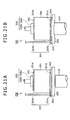
- FIGS. 21A and 21B are schematic views each showing a concrete construction of a conventional variable capacitor.
- FIG. 21A is a schematic view showing an initial state in the conventional variable capacitor
- FIG. 21B is a schematic view showing a state in which a pressure is applied to the conventional variable capacitor.
- the variable capacitor 200 includes a dielectric 201 having approximately a disc-like shape, a first electrode 202, and a second electrode 203.
- the first electrode 202 is mounted on one surface 201 a of the dielectric 201.
- the second electrode 203 is disposed on the other surface 201 b opposite to the one surface 201a of the dielectric 201.
- the second electrode 203 has flexibility and is disposed on the other surface 201b of the dielectric 201 through a ring-like spacer 204.
- a rod-like core body 210 is provided on a side of the second electrode 203 opposite to the dielectric 201 side through an elastic body 205.
- a first terminal 206 is provided on the one surface side of the first electrode 202.
- the first terminal 206 is composed of a disc-like flange portion 206a, and a lead portion 206b extending approximately from a center of one surface of the disc-like flange portion 206a.
- the flange portion 206a comes in contact with one surface of the first electrode 202 to be electrically connected to the first electrode 202.
- a second terminal 207 is provided in an end (edge) portion of the second electrode 203.
- the second terminal 207 is composed of a disc-like flange portion 207a and a lead portion 207b extending approximately from a center of one surface of the flange portion 207a similarly to the case of the first terminal 206.
- the flange portion 207a is in contact with an end portion of one surface of the second electrode 203 and is electrically connected to the first electrode 203.
- variable capacitor 200 in a state in which neither the pressure nor the displacement is applied to the core body 210 (initial state), a small space is defined between the other surface 201b of the dielectric 201 and the second electrode 203 by a spacer 204.
- a spacer 204 As shown in FIG. 21B , when the pressure is applied to the core body 210, both of the elastic body 205 and the second electrode 203 are depressed by the core body 210 to be elastically deformed. As a result, the second electrode 203 comes in contact with the other surface 201b of the dielectric 201.
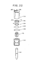
- the conventional variable capacitor 200 described with reference to FIGS. 21A and 21B is actually formed within a housing member. Specifically, with respect to assembly of the variable capacitor 200, as shown in FIG. 22 , the dielectric 201 having the first electrode 202 provided thereon, the spacer 204, the second electrode 203, and the elastic body 205 are laminated in this order to be formed within the housing member 221.
- the first terminal 206 is connected to the first electrode 202
- the second terminal 207 is connected to the end (edge) portion of the second electrode 203.
- both of a cap body 72 for holding the core body 210 and a second housing member 222 are inserted from a lower side of the first housing member 221 into the first housing member 221, thereby forming one variable capacitor 200.
- the conventional variable capacitor 200 is formed from the nine parts or components: (1) the first terminal 206; (2) the second terminal 207; (3) the first housing member 221; (4) the dielectric 201 having the first electrode 202 provided thereon; (5) the spacer 204; (6) the second electrode 203; (7) the elastic body 205; (8) the cap body 72 for holding the core body 210; and (9) the second housing member 222.
- the size of the conventional variable capacitor 200 is relatively small because the conventional variable capacitor 200 is accommodated in a pen-type position indicator. For this reason, it is rather difficult and time-consuming to manufacture the conventional variable capacitor 200 in some cases.
- the invention relates to a variable capacitor according to claim 1.
- Claims 2 to 15 refer to specifically advantageous realizations of the subject matter of claim 1.
- variable capacitor which is simpler to construct, without having its performance compromised. Further, a position indicator using such variable capacitor, and an input device including such position indicator are provided.
- a variable capacitor for use with an electronic circuit board including a first terminal portion and a second terminal portion, which are all to be built in a position indicator.
- the variable capacitor includes a dielectric having a first surface portion and a second surface portion opposite to said first surface portion, and a conductive elastic member having a board coupling portion and a dielectric contacting portion.
- the first terminal portion is coupled to the first surface portion
- the second terminal portion is coupled to the board coupling portion
- the dielectric contacting portion is disposed separately from the second surface portion so as to face the second surface portion and is further configured to be deformed to come in contact with the second surface portion of the dielectric.
- a contact area between the second surface portion and the dielectric contacting portion is changed in correspondence to a depressing force, which is applied against the dielectric contacting portion in a direction toward the dielectric, thereby changing an electrostatic capacitance of the variable capacitor.
- the first terminal portion of the electronic circuit board is coupled to the first surface portion of the dielectric
- the second terminal portion of the electronic circuit board is coupled to the board coupling portion of the conductive elastic member.
- the dielectric contacting portion of the conductive elastic member is disposed separately (spaced) from the second surface portion of the dielectric so as to face the second surface portion of the dielectric, but is configured to be deformed toward the second surface portion when a depressing force is applied.
- the dielectric contacting portion and the second surface portion of the dielectric come in contact with each other when the depressing force is applied.
- the contact area between the dielectric contacting portion and the second surface portion of the dielectric is changed, thereby changing the electrostatic capacitance of the variable capacitor.
- a connection system is formed as follows: the first terminal portion of the electronic circuit board ⁇ the first surface portion of the dielectric ⁇ the second surface portion of the dielectric ⁇ the dielectric contacting portion of the conductive elastic member ⁇ the board coupling portion of the conductive elastic member ⁇ the second terminal portion of the electronic circuit board.
- the variable capacitor is provided whose electrical capacitance changes in accordance with the contact state, corresponding to the depressing force, between the second surface portion of the dielectric and the dielectric contacting portion of the conductive elastic member.
- variable capacitor which has a very simple construction including two members: the dielectric and the conductive elastic member.
- performance of the variable capacitor is not degraded as compared with that of a conventional variable capacitor. In other words, it is possible to realize a variable capacitor, which is simpler to construct and yet maintains high performance.
- a position indicator including the variable capacitor as described above, an electronic circuit board having electronic circuit provided therein, and a resonance circuit having the variable capacitor as its element.
- an input device including a position indicator and a position detector having a detection surface configured to detect a position indicated by the position indicator.
- the position indicator includes a case, an elongated core body accommodated within the case and having one end thereof protruding from the case while having another end thereof accommodated within the case, a variable capacitor whose electrical capacitance changes when an external force is applied thereto through the core body, and an electronic circuit board having a first terminal portion and a second terminal portion.
- the variable capacitor of the position indicator includes a dielectric having a first surface portion and a second surface portion opposite to the first surface portion, and a conductive elastic member having a board coupling portion and a dielectric contacting portion.
- the first terminal portion is coupled to the first surface portion
- the second terminal portion is coupled to the board coupling portion
- the dielectric contacting portion is disposed separately from the second surface portion so as to face the second surface portion and is configured to be deformed to come in contact with said second surface portion.
- a contact area between the second surface portion and the dielectric contacting portion is changed in correspondence to a depressing force, which is applied against the dielectric contacting portion in a direction toward the dielectric, thereby changing an electrostatic capacitance of the variable capacitor.
- variable capacitor which is simpler to construct and maintains high performance.
- position indicator using the variable capacitor, and an input device using such position indicator including the variable capacitor.
- an accommodating portion claimed in the appended claims is embodied as a holding hole 15ch for a board and the like.
- a board coupling portion claimed in the appended claims is embodied as a groove portion 15ck provided in a holder portion 15cl for a board and the like in one embodiment.
- a core coupling portion claimed in the appended claims is embodied as a core body holding hole 15cp and a core body holder 15c2 in one embodiment.
- FIG. 1 is a perspective view showing the schematic construction of the embodiment of the input device according to the present invention.
- the input device 10 is composed of a position detector 1, and a position indicator 2 for inputting information to the position detector 1.
- the position detector 1 is connected to an external apparatus such as a personal computer or a Personal Digital Assistant (PDA) via a cable 8, whereby the position detector 1 is used as an input device for such an external apparatus. It is noted that although not specifically illustrated, such a position detector 1 may be built in the personal computer or the like.
- PDA Personal Digital Assistant
- the position detector 1 is composed of a detecting portion 4 and a chassis 5.
- the detecting portion 4 detects a position indicated by the position indicator 2, which will be described later.
- the chassis 5 forms approximately a hollow thin rectangular parallelepiped and has the detecting portion 4.
- the chassis 5 has an upper chassis 7 and a lower chassis (not shown).
- the upper chassis 7 has an opening portion 6 for exposing a detection surface of the detecting portion 4.
- the upper chassis 7 is superposed on the lower chassis (not shown).
- the detecting portion 4 is fitted into the quadrangular opening portion 6 of the upper chassis 7, so that the input surface of the detecting portion 4 is exposed through the quadrangular opening portion 6.
- the position detector 1 having such a construction receives an input of characters, figures or the like, made by a pointing operation of the position indicator 2, which will be described below.
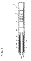
- FIG. 2 is a cross sectional view taken along line A-A' of the position indicator 2 shown in FIG. 1 .
- the position indicator 2 serves to indicate a position for the position detector 1 by using an electromagnetic induction system.
- the position indicator 2 has a resonance circuit which enters into resonance with an electric wave having a specific frequency and transmitted thereto from the position detector 1.
- the position indicator 2 transmits a resonance signal detected by the resonance circuit to the position detector 1, thereby indicating a position for the position detector 1.
- the position indicator 2 is constructed so as to include a case 11 showing a concrete example of a chassis, a core body 12, a position indicating coil 13, a variable capacitor 15, a ferrite core 16, and a printed wiring board 17.
- the case 11 is formed as an external packaging portion of the position indicator 2.
- the case 11 has a bottomed cylindrical shape whose one end is closed.
- the case 11 is composed of a first case 18 and a second case 19 which are assembled, and coupled with the first case 18 and the second case 19 being axially superposed on each other.
- the first case 18 has approximately a conical shape at one end side in an axial direction, and has an opening portion 18a at a tip of that one end side. The other end of the first case 18 in the axial direction is open.
- the second case 19 has a cylindrical shape whose one end in the axial direction is open and whose other end is closed.
- the first case 18 and the second case 19 are disposed on the same axis line, and are fixed to each other by using a firmly fixing section such as an adhesive agent or fixing screws.
- the printed wiring board 17 having electronic parts or components mounted thereto is firmly fixed to the second case 19 by using a firmly fixing section such as an adhesive agent or fixing screws.
- the ferrite core 16 is accommodated in the first case 18.
- the ferrite core 16 for example, has a cylindrical shape, and a core body 12 is inserted into a cylindrical hole 16a of the ferrite core 16. An indication portion 12a of the core body 12 protrudes from one end side in the axial direction of the ferrite core 16.
- a position indicating coil 13 composing a resonance circuit is wound around the outer periphery of the ferrite core 16 to be mounted thereto. Both ends (not shown) of the position indicating coil 13 are electrically connected to opposite terminals of corresponding one of the electronic parts or components firmly fixed to the printed wiring board 17, respectively. Electronic parts or components composing the resonance circuit are mounted to the printed wiring board 17.
- the core body 12 is made from approximately a rod-like member, and is accommodated in the case 11 along the axial direction of the case 11.
- the core body 12 is composed of the indication portion 12a, and an axis portion 12b.
- the indication portion 12a has a role of a pen tip at one end of the core body 12 in the axial direction.
- the axis portion 12b is continuously formed from the indication portion 12a.
- the indication portion 12a is formed approximately in a conical shape.
- the indication portion 12a protrudes from the opening portion 18a of the first case 18 toward the outside when the core body 12 is accommodated in the case 11.
- the variable capacitor 15 is mounted to the other end of the axis portion 12b in the axial direction.
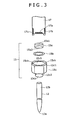
- FIG. 3 is an exploded perspective view of the variable capacitor 15.
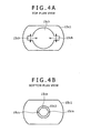
- FIGS. 4A and 4B are a top plan view and a bottom plan view, respectively, of a conductive elastic member 15c of the variable capacitor 15.
- FIG. 5 is a cross sectional view of the variable capacitor 15 portion when both of the printed wiring board 17 and the core body 12 are mounted to the variable capacitor 15.
- FIGS. 6A and 6B are cross sectional views explaining an example of joining between the printed wiring board 17 and a dielectric 15a.
- the variable capacitor 15 is a capacitor whose capacitance value is changed so as to correspond to a pressure (pen pressure) applied to the position indicator 2.
- the variable capacitor 15 detects the pen pressure applied to the core body 12 as a corresponding change in capacitance value, and thus serves as a pen pressure detecting portion of the position indicator 2.
- the variable capacitor 15 is composed of the dielectric 15a, a spacer (spacing member) 15b, and the conductive elastic member 15c.
- the dielectric 15a, the space (spacing member) 15b, and the conductive elastic member 15c are held between the printed wiring board 17 and the core body 12, to be used as the variable capacitor 15 of the position indicator 2.
- the dielectric 15a is formed in a columnar shape having a first surface portion 15a1 and a second surface portion 15a2 opposite to each other.
- the dielectric 15a is 2.95 mm in outer diameter, 1 mm in thickness, and 160 pF (permittivity: 4,000 F/m) in capacitance value.
- the unit, mm means a millimeter
- the unit, pF means a picofarad
- the unit, F/m means a meter per farad.
- the dielectric 15a is examples only, and thus various numerical values can be adopted in accordance with the size of the position indicator 2 having the variable capacitor 15 mounted thereto, the size of the printed wiring board 17, and the like.
- the second surface portion 15a2 of the dielectric 15a is subjected to mirror polishing, thereby increasing the degree of adhesion to a dielectric contacting portion 15cX of the conductive elastic member 15c (see FIG. 5 ), which will be described later.
- various kinds of materials such as ceramics and plastic can be used as the material for the dielectric 15a as long as they meet the conditions of the capacitance, the permittivity, and the like.
- the spacer (spacing member) 15b is formed in a ring-like (annular) shape.
- An inner diameter of the spacer 15b is smaller than a diameter of the dielectric 15a and an outer diameter of the spacer 15b is larger than the diameter of the dielectric 15a and is slightly smaller than an inner diameter of the conductive elastic member 15c, which will be described later, into which the spacer is accommodated.
- Adoption of such a construction can prevent position shift of the spacer 15b within the conductive elastic member 15c.
- the spacer 15b is set to be about 2.6 mm in inner diameter, and about 4.3 mm in outer diameter.
- the thickness of the spacer 15b is set equal to or smaller than 125 ⁇ m, for example.
- the numerical values shown here are examples only, and thus suitable material values can be adopted based on the size and the like of the dielectric 15 a.
- the spacer 15b may be formed from a Polyethylene Terephthalate (PET) film or a polyimide film, for example.
- a holder portion 15cl for a board and the like, and the core body holder portion 15c2, are formed integrally with each other, by using a conductive rubber, into the conductive elastic member 15c.
- the holder portion 15c1 for a board and the like is a cylindrical portion which has an opening portion having a diameter slightly larger than the outer diameter of the spacer 15b, and which is provided with a holding hole (accommodating portion) 15ch for a board and the like having a predetermined depth while maintaining an area of the opening portion.
- the spacer 15b, the dielectric 15a, and a terminal portion of the printed wiring board 17 are accommodated in order from the lower side in the holding hole 15ch for a board and the like to be held therein.
- a side of the holder portion 15c1 for a board and the like opposite to the opening portion thereof is provided with a closed bottom surface. This bottom surface composes the dielectric contacting portion 15cX, which is configured to contact the second surface portion 15a2 of the dielectric 15a (see FIG. 5 ).
- a paired groove portions 15ck composing a board coupling portion are provided in respective positions facing each other of the outer periphery of the holding hole 15ch for a board and the like of the holder portion 15c1 for a board and the like. That is to say, as shown in a top plan view of the conductive elastic member 15c of FIG. 4A , a construction is adopted such that the paired groove portions 15ck composing the board coupling portion into which the printed wiring board 17 is inserted are provided in the respective positions facing each other of the opening portion of the holding hole 15ch for a board and the like of the holder portion 15cl for a board and the like.
- a depth of each of the paired groove portions 15ck is set slightly shallower (shorter) than that of the holding hole 15ch for a board and the like (see FIG. 5 ).
- a width, w, of each of the paired groove portions 15ck shown in FIG. 4A is set slightly narrower than a thickness of the printed wiring board 17 inserted into the paired grooves 15ck.
- the holder portion 15cl for a board and the like has a shape as shown in FIG. 4A , in which outer peripheral portions in a direction (in a vertical direction in FIG. 4A ) intersecting with a diameter direction connecting the paired groove portions 15ck are cut away. Adoption of such a shape results in that the conductive elastic member 15c, which is hard to roll and is easy to handle, can be formed without wastefully using a conductive rubber.
- the core body holder 15c2 is provided in such a way that a (closed) bottom surface thereof is flush with the bottom surface of the holder portion 15cl for a board and the like.
- the core body holder portion 15c2 is provided in such a way that an outer diameter thereof is smaller than that of the holder portion 15c1 for a board and the like, and a center of the bottom surface of the holder portion 15c1 for a board and the like, and a center of the bottom surface of the core body holder 15c2 agree with each other.
- the core body holder 15c2 is a cylindrical portion which has an opening portion having a diameter slightly smaller than an outer diameter of the axis portion 12b of the core body 12 and which is provided with a core body holding hole (core body coupling portion) 15cp having a predetermined depth while maintaining an area of the opening portion. As shown in FIG. 3 , the axis portion 12b of the core body 12 is inserted into the core body holding hole 15cp to be held.
- a construction is adopted such that paired slit portions (cut portions) 15cs are provided in respective positions facing each other of the opening portion of the core body holding hole 15cp of the core body holder portion 15c2.
- a depth of each of the paired slit portions 15cs is set slightly shallower (shorter) than that of the core body holding hole 15cp. Provision of the paired slit portions 15cs results in that it is easy to insert the core body 12 into the core body holding hole 15cp.
- the conductive rubber composing the conductive elastic member 15c is a synthetic rubber with which a conductive particle such as a carbon particle or a silver particle is mixed, and is a material having the flexibility and the elasticity as well as the conductivity.
- conductive rubber is classified into one of two types: a rubber of a type in which an electrical resistance value depends on a pressure, that is, a rubber (pressure-sensitive rubber) of a type having a tendency such that a resistance value becomes small as a depressing force applied is larger, and a rubber (narrow conductive rubber) of a type in which an electrical resistance value does not depend on a pressure. Any of the two types of rubbers can be used as the material composing the conductive elastic member 15c.
- flexibility is a property capable of being bent, or a property capable of being pliant.
- flexibility means that a material can be deformed when a depressing force is applied thereto, and can be restored back to the original state when the depressing force is removed. In this case, whether or not a size of the material itself is changed with respect to (along) the depressing direction is not relevant.
- elasticity means that a size of a material itself is reduced along a depressing direction when a depressing force is applied to the material, and the material can be returned back to the original state when the depressing force is removed.
- the conductive elastic member 15c (having flexibility) in the embodiment can be bent or contracted when the pressure is applied thereto and can be restored back to the original state when the pressure is removed.
- variable capacitor 15 in the embodiment of the input device both of the dielectric 15a and the spacer 15b are accommodated in the holding hole 15ch for a board and the like provided in the holder portion 15cl for a board and the like of the conductive elastic member 15c. Also, the dielectric 15a, the spacer 15b, and the conductive elastic member 15c are held between the printed wiring board 17 and the core body 12, thereby serving as the variable capacitor 15 of the position indicator 2.
- each of the two lateral side portions of the end portion is set slightly longer than a bottom side portion held between the two lateral side portions of the end portion.
- a first lead piece (first terminal portion) 17a is provided in the bottom side portion of the printed wiring board 17, and second lead portions (second terminal portions) 17b are provided in both of the lateral side portions, respectively.
- the first terminal portion 17a and the second terminal portions 17b are connected to a predetermined circuit portion(s) provided on the printed wiring board 17 through respective lead lines (not shown).
- the first lead piece 17a of the printed wiring board 17 is electrically connected to the first surface portion 15al of the dielectric 15a, and the dielectric 15a itself is firmly fixed to the printed wiring board 17.
- the first lead piece 17a of the printed wiring board 17 and the first surface portion 15al of the dielectric 15a are joined to each other by, for example, using a method such as a soldering method or a brazing method.
- a method such as a soldering method or a brazing method.
- the first lead piece 17a of the printed wiring board 17, and the first surface portion 15al of the dielectric 15a are electrically connected to each other, and the dielectric 15a is firmly fixed to the printed wiring board 17.
- the soldering method or the brazing method is an example of the firmly fixing method.
- the first lead piece 17a, and the first surface portion 15al of the dielectric 15a may be electrically connected to each other by using any of various kinds of conductive adhesive agents, and thus the dielectric 15a may be firmly fixed to the printed wiring board 17.
- Both of the end portions of the lateral sides of the printed wiring board 17 are respectively fitted into the paired groove portions (board coupling portions) facing each other and provided in the outer peripheral portion of the holding hole 15ch for a board and the like of the holder portion 15c1 for a board and the like of the conductive elastic member 15c.
- the second lead pieces 17b provided in both of the lateral side portions of the printed wiring board 17, respectively are electrically connected to the conductive elastic member 15c.
- the ring-like spacer 15b is accommodated in the holding hole 15ch for a board and the like provided in the holder portion 15cl for a board and the like of the conductive elastic member 15c so as to contact the bottom surface of the holding hole 15ch for a board and the like.
- the first surface portion 15al is electrically connected to the first lead piece 17a of the printed wiring board 17, and also the dielectric 15a firmly fixed to the printed wiring board 17 is accommodated together with the printed wiring board 17 from the opening portion of the holding hole 15ch for a board and the like.
- both of the lateral side portions provided with the second lead pieces 17b of the printed wiring board 17, respectively are fitted into the paired groove portions (board coupling portions) 15ck facing each other and provided in the outer peripheral portion of the holding hole 15ch for a board and the like.
- the second lead pieces 17b provided in both of the lateral side portions of the printed wiring board 17, respectively are electrically connected to the conductive elastic member 15c through the respective groove portions 15ck composing the board coupling portions.
- the bottom surface portion of the holding hole 15ch for a board and the like of the holder portion 15c1 for a board and the like composing the dielectric contacting portion 15cX, and the second surface portion 15a2 of the dielectric 15a are separated (spaced) from each other by a thickness of the spacer 15b by the spacer 15b. That is to say, a space 15d is defined between the bottom surface portion of the holding hole 15ch for a board and the like of the holder portion 15cl for a board and the like composing the dielectric contacting portion 15cX, and the second surface portion 15a2 of the dielectric 15a by the spacer 15b.
- the axis portion 12b of the core body 12 is fitted into the core body holding hole 15cp of the core body holder portion 15c2 of the conductive elastic member 15c. It is then supposed that a depressing force is applied to the dielectric 15a side of the core body 12 when, for example, the indication portion 12a of the core body 12 is pressed against the detecting portion 4 of the position detector 1.
- the conductive elastic member 15c has elasticity and flexibility as well as conductivity. Therefore, the bottom surface portion (the dielectric contacting portion 15cX) of the holding hole 15ch for a board and the like of the board holder portion 15cl is upward pressed toward the second surface portion 15a2 side of the dielectric 15a by the core body 12. Also, the application of the depressing force toward the dielectric 15a by the core body 12 results in that the bottom surface portion (the dielectric contacting portion 15cX) of the holding hole 15ch for a board and the like comes in contact with the second surface portion 15a2 of the dielectric 15a.
- the conductive elastic member 15c is returned back to the original state by the elasticity and flexibility of the conductive elastic member 15c.
- the operation state is returned back to the state such that the space 15d is defined between the bottom surface portion (the dielectric contacting portion 15cX) of the holding hole 15ch for a board and the like, and the second surface portion 15a2 of the dielectric 15a by the spacer 15b.
- the space 15d is defined between the bottom surface portion (the dielectric contacting portion 15cX) of the holding hole 15ch for a board and the like, and the second surface portion 15a2 of the dielectric 15a, and therefore electrical connection is not formed.
- the bottom surface portion (the dielectric contacting portion 15cX) of the holding hole 15ch for a board and the like, and the second surface portion 15a2 of the dielectric 15a come in contact with each other.
- a connection system as follows: the first lead piece 17a of the printed wiring board 17 ⁇ the first surface portion 15al of the dielectric 15a ⁇ the second surface portion 15a2 of the dielectric 15a ⁇ the dielectric contacting portion 15cX of the conductive elastic member 15c ⁇ the board coupling portion 15ck of the conductive elastic member 15c ⁇ the second terminal portion 17b of the printed wiring board 17.
- variable capacitor 15 is constructed whose electrical capacitance is changed in accordance with the contact state, corresponding to the depressing force, between the second surface portion 15a2 of the dielectric 15a, and the dielectric connecting portion 15cX of the conductive elastic portion 15c in the connection system.
- variable capacitor 15 in the illustrated embodiment can be basically composed of the three parts or components: the dielectric 15a; the spacer 15b; and the conductive elastic member 15c.
- the variable capacitor 15 having a very simple construction can be realized in this manner.
- variable capacitor 15 of the embodiment for the purpose of reliably and firmly fixing the printed wiring board 17 to the first surface portion 15a1 of the dielectric 15a, a sample construction of a connection end of the printed wiring board 17 to (be connected to) the conductive elastic member 15c is provided and now described.
- a semi-circular through hole (a cutout portion (or a holding hole) for holding the solder as the conductive adhesive agent) 17c is provided in the first lead piece 17a portion of the connection end of the printed wiring board 17, to be connected to the conductive elastic member 15c.
- the bottom side portion of the printed wiring board 17 is cut into the semi-circular shape to provide the through hole 17c.
- the first lead piece 17a is provided so as to have an arc-like shape along the outer peripheral portion of the semi-circular through hole 17c.
- the first surface portion 15al of the dielectric 15a is made to come in contact with the through hole 17c portion of the printed wiring board 17 constructed in such a way, and a solder 17x as the conductive adhesive agent is caused to flow into the through hole 17c portion, thereby carrying out the soldering.
- the through hole 17c is filled with the solder 17x.
- the solder 17x portion is solidified, the first surface portion 15al of the dielectric 15a, and the first lead piece 17a of the printed wiring board 17 are electrically connected to each other and also the dielectric 15a is firmly fixed to the printed wiring board 17.
- the construction is adopted such that the through hole 17c is provided in the connection end of the printed wiring board 17 to be connected to the conductive elastic member 15c, and the arc-like lead piece 17a is provided in the outer peripheral portion of the through hole 17c.
- the first lead piece 17a of the printed wiring board 17 and the first surface portion 15al of the dielectric 15a can be electrically connected to each other and also the dielectric 15a can be firmly fixed to the printed wiring board 17.
- the through hole 17c has been described as being semi-circular here, the present invention is by no means limited thereto.
- a through hole having a polygonal shape such as a triangular shape or a quadrangular shape may be provided, and the first lead piece may be provided in an outer periphery or edge of the through hole.
- variable capacitor 15 composes the pen pressure detecting portion in the position indicator 2. Next, a description will be given regarding the precision in detection of the pen pressure (pressure) by the variable capacitor 15 of the embodiment described above.
- FIG. 7 is a graph showing phase-load characteristics of the variable capacitor 15 with a load applied to the core body 12 on an axis of abscissa, and a phase (a difference in phase between a transmitted electric wave and a received electric wave) on an axis of ordinate.
- variable capacitor 15 of the embodiment described above has a very simple construction, as shown in FIG. 7 , the variable capacitor 15 can detect a load (pressure) of about 10g. Also, the variable capacitor 15 can approximately linearly detect the applied load up to about 100 g with high sensitivity. The applied load above 100 g up to about 300 g can be suitably detected as well. Although a change in phase difference against the applied load of 300 g or more becomes small, since application of a large pen pressure of 300 g or more to the position indicator 2 is rare, practical utility of the position indicator 2 using the variable capacitor 15 is not compromised at all.
- variable capacitor 15 shown in FIG. 7 are approximately the same as the characteristics of the position indicator using the conventional variable capacitor described with reference to FIGS. 21A and 21B , and FIG. 22 , for example. Therefore, although the variable capacitor 15 of the illustrated embodiment is simple in construction, the variable capacitor 15 maintains the same performance as compared with the conventional variable capacitor.
- FIG. 8 is a block diagram, partly in circuit, showing the position indicator 2 and the position detector 1.
- the input device is composed of the position indicator 2 and the position detector 1.
- the position indicator 2 is configured by a resonance circuit 61 composed of the position indicating coil 13, the variable capacitor 15 connected in parallel with the position indicating coil 13, and a resonance capacitor 60a connected in parallel with the variable capacitor 15 in terms of a circuit configuration.
- the resonance circuit 61 changes its resonance frequency in accordance with a change in electrical capacitance of the variable capacitor 15, and the change in resonance frequency is detected as a pen pressure.
- an X-axis direction loop coil group 104a, and a Y-axis direction loop coil group 104b are laminated and provided, thereby forming a position detecting coil 101.
- Each of the X-axis direction loop coil group 104a, and the Y-axis direction loop coil group 104b is composed of 40 rectangular loop coils, for example.
- the rectangular loop coils composing each of the X-axis direction loop coil group 104a and the Y-axis direction loop coil group 104b are disposed in such a way that they are arranged at equal intervals to be superposed one upon another.
- the position detector 1 is provided with a selecting circuit 106, to which both of the X-axis direction loop coil group 104a and the Y-axis direction loop coil group 104b are connected.
- the selecting circuit 106 successively selects one loop coil from the X-axis direction loop coil group 104a and the Y-axis direction loop coil group 104b.
- the position detector 1 is provided with an oscillator 103, a current driver 105, a switchover connecting circuit 107, a receiving amplifier 108, a detector 109, a low-pass filter 110, a sample-and-hold circuit 112, an A/D conversion circuit 113, a synchronous detector 116, a low-pass filter 117, a sample-and-hold circuit 118, an A/D conversion circuit 119, and a processing portion 114.
- the oscillator 103 is one which generates an A.C. signal having a frequency, f0, and supplies the resulting A.C. signal to each of the current driver 105 and the synchronous detector 116.
- the current driver 105 converts the A.C. signal supplied thereto from the oscillator 103 into an A.C. current, and sends the resulting A.C. current to the switchover connecting circuit 107.
- the switchover connecting circuit 107 switches connection destinations (a transmission side terminal T and a reception side terminal R), to which the loop coil selected by the selecting circuit 106 is connected in accordance with the control made by the processing portion 114, which will be described later. Of the connection destinations, the current driver 105 is connected to the transmission side terminal T, and the reception amplifier 108 is connected to the reception side terminal R.
- An induced voltage generated in the loop coil selected by the selecting circuit 106 is sent to the reception amplifier 108 through the selecting circuit 106 and the switchover connecting circuit 107.
- the reception amplifier 108 amplifies the induced voltage supplied thereto from the selected loop coil, and sends the induced voltage thus amplified to each of the detector 109 and the synchronous detector 116.
- the detector 109 detects the induced voltage generated in the selected loop coil, that is, the received signal, and sends the received signal thus detected to the low-pass filter 110.
- the low-pass filter 110 has a sufficient lower cutoff frequency than the frequency, f0, described above, converts the output signal from the detector 109 into a D.C. signal, and sends the resulting D.C. signal to the sample-and-hold circuit 112.
- the sample-and-hold circuit 112 holds an analog voltage value at a predetermined timing of the output signal from the low-pass filter 110, specifically, at a predetermined timing during a period of time for reception, and sends the analog voltage to the Analog-to-Digital (A/D) conversion circuit 113.
- the A/D conversion circuit 113 converts the analog output from the sample-and-hold circuit 112 into a digital signal, and outputs the resulting digital signal to the processing portion 114.
- the synchronous detector 116 detects the output signal from the reception amplifier 108 synchronously with the A.C. signal from the oscillator 103, and sends a signal having a level corresponding to a difference in phase between the output signal and the A.C. signal to the low-pass filter 117.
- the low-pass filter 117 has a sufficiently lower cutoff frequency than the frequency, f0, and converts the output signal from the synchronous detector 116 into a D.C. signal and sends the resulting D.C. signal to the sample-and-hold circuit 118.
- the sample-and-hold circuit 118 holds an analog voltage value at a predetermined timing of the output signal from the low-pass filter 117, and sends the analog voltage to the Analog-to-Digital (A/D) conversion circuit 119.
- the A/D conversion circuit 119 converts the analog voltage from the sample-and-hold circuit 118 into a digital signal, and outputs the resulting digital signal to the processing portion 114.
- the processing portion 114 controls the operations of the portions in the position detector 1. In other words, the processing portion 114 controls the selection of the loop coil in the selecting circuit 106, the switchover of the switchover connecting circuit 107, and the timings of the sample-and-hold circuits 112 and 118.
- the processing portion 114 causes the X-axis direction loop group 104a and the Y-axis direction loop group 104b to transmit the electric wave for a given transmission duration in accordance with the input signals from the A/D conversion circuits 113 and 119.
- the induced voltage is generated in each of the loop coils of the X-axis direction loop group 104a and the Y-axis direction loop group 104b based on the electric wave transmitted from the position indicator 2.
- the processing portion 114 calculates the coordinate values of the indicated position in the X-axis direction and in the Y-axis direction in accordance with the level of the voltage value of the induced voltage generated in corresponding one of the loop coils.
- the processing portion 114 detects the pen pressure in accordance with the difference in phase between the transmitted electric wave and the received electric wave.
- FIG. 9 is a flow chart representing the flow of the processing in the processing portion 114.
- Step S1 the processing portion 114 successively scans and selects the loop coils of the X-axis direction loop group 104a (hereinafter, this successive scan and selection will be referred to as "global scan") (Step S1).
- the processing portion 114 firstly sends information, in accordance with which the first loop coil of the X-axis direction loop coil group 104a, for example the loop coil X1, is selected by the selecting circuit 106, and also sends a signal, in accordance with which the transmission side is selected by the switchover connecting circuit 107.
- a sine wave signal having the frequency f0 is supplied from the oscillator 103 to the loop coil X1, so that the loop coil X1 generates the electric wave having the frequency, f0.
- the position indicator 2 either approaches or contacts the upper surface of the detecting portion 4 of the position detector 1
- the electric wave generated from the loop coil X1 excites the resonance circuit 61 having the position indicating coil 13.
- the induced voltage having the frequency f0 is generated in the resonance circuit 61.
- the processing portion 114 After the processing portion 114 sends a signal, in accordance with which the transmission side terminal T is selected by the switchover connecting circuit 107 for a given period of time, the processing portion 114 sends a signal, in accordance with which the reception side terminal R is selected by the switchover connecting circuit 107, thereby causing the electric wave generated from the loop coil X1 to disappear.
- the induced voltage generated in the resonance circuit 61 of the position indicator 2 having the resonance capacitor 60a and the variable capacitor 15 gradually attenuates correspondingly, so that the resonance circuit 61 transmits the electric wave.
- the electric wave reversely excites the loop coil X1 described above, thereby causing the loop coil X1 to generate the induced voltage.
- the processing portion 114 After the processing portion 114 sends a signal, in accordance with which the reception side terminal R is selected by the switchover connecting circuit 107 for a given period of time, the processing portion 114 sends information, in accordance with which the selecting circuit 106 is caused to select the second loop coil from the X-axis direction loop group 104a, for example the loop coil X2, to be connected to the switchover connecting circuit 107. After that, the processing portion 114 sends a signal, in accordance with which the transmission side terminal T is selected by the switchover connecting circuit 107, thereby carrying out the same transmission and reception of the electric wave as those in the foregoing.
- the processing portion 114 executes the same processing as that of the foregoing, whereby the loop coils from the third to 40-th loop coils of the X-axis direction loop coil group 104a, for example the loop coils X3 to X40, are successively scanned and selected. As a result, the transmission and reception of the electric wave are carried out in the loop coils X3 to X40 in order.
- the processing portion 114 may suitably limit the loop coils to be selected such as every other loop coil or one in every two loop coils.
- the transmission and reception of the electric wave for one loop coil may be carried out plural times.
- the transmission time for each of the loop coils need to be the same, and the reception time for each of the loop coils need to be the same, the transmission time and the reception time need not be identical to each other.
- the induced voltage generated in the loop coil of the X-axis direction loop coil group 104a for the period of time for reception described above, that is, the A.C. received signal, is detected by the detector 109 to be converted into a D.C. signal and smoothed in the low-pass filter 110.
- the resulting D.C. signal is held at the predetermined timing by the sample-and-hold circuit 112, and is then sent as a voltage value to the processing portion 114 through the A/D conversion circuit 113.
- FIGS. 10A to 10D show an example of waveforms in the portions in the X-axis global scanning operation (Step S 1 in FIG. 9 ) described above.
- FIG. 10A shows the waveforms of the electric wave transmitted from the position detecting coil 101.
- FIG. 10B shows the waveforms of the induced voltage generated in the resonance circuit 61
- FIG. 10C shows the waveforms of the received signal received by the position detector 1
- FIG. 10D shows the waveforms of the output signal from the sample-and-hold circuit 112.
- a level of the output signal from the sample-and-hold circuit 112 is a value depending on a distance between the position indicator 2 and the loop coil. For this reason, the processing portion 114 determines whether or not a maximum value of the level of the output signal from the sample-and-hold circuit 112 is equal to or larger than a given value previously set (Step S2), thereby determining whether or not a height of the position indicator 2 falls within an effective read height of the position detector 1.
- Step S2 When it is determined in the processing in Step S2 that the maximum value of the level of the output signal from the sample-and-hold circuit 112 is not equal to or larger than the given value previously set, that is, the height of the position indicator 2 does not fall within the effective read height of the position detector 1 (NO in Step S2), the processing portion 114 returns the operation back to the processing in Step S 1.
- the processing portion 114 extracts the loop coil from which the maximum value is obtained (hereinafter referred to as "a peak coil”) from the loop coils X1 to X40, and stores a number of the peak coil ("X7" in this case) (Step S3).
- the processing portion 114 successively scans and selects (global scan) the loop coils of the Y-axis direction loop coil group 104b (Step S4), and carries out the transmission and reception of the electric waves in the loop coils of the Y-axis direction loop coil group 104b.
- FIGS. 11A to 11D show an example of waveforms in the portions in a Y-axis global scanning operation.
- the signals shown in waveforms in FIGS. 11A to 11D are the same signals as those shown in FIGS. 10A to 10D , respectively.
- the processing portion 114 extracts the loop coil from which the maximum value is obtained (hereinafter referred to as "a peak coil") of the loop coils Y1 to Y40, and stores a number of the peak coil ("Y5" in this case) (Step S5).
- the processing portion 114 carries out the transmission and reception of the electric waves for a predetermined number of X loop coils adjacent to the X peak coil, for example, five loop coils with the peak coil of the X-axis direction loop coil group 104a as a center.
- the processing portion 114 when the electric wave is transmitted, that is, when the transmission side terminal T is selected in the switchover connecting circuit 107, the processing portion 114 usually selects the peak coil ("the loop coil X7" in this case).
- the processing portion 114 when the electric wave is received, that is, when the reception side terminal R is selected in the switchover connecting circuit 107, the processing portion 114 successively scans and selects (sector scan) the loop coils (the five loop coils in this case) in the ascending order in number (or in the descending order in number) (Step S6).
- the processing portion 114 carries out the transmission and reception of the electric waves for a predetermined number of Y loop coils adjacent to the Y peak coil, for example, five loop coils with the peak coil of the Y-axis direction loop coil group 104a as a center.
- the processing portion 114 when the electric wave is transmitted, that is, when the transmission side terminal T is selected in the switchover connecting circuit 107, the processing portion 114 usually selects the peak coil ("the loop coil Y5" in this case).
- the processing portion 114 successively scans and selects (sector scan) the loop coils (the five loop coils in this case) in the ascending order in number (or in the descending order in number) (Step S7).
- FIGS. 12A to 12D show an example of waveforms in the portions in the X-axis sector scanning operation and the Y-axis sector scanning operation.
- the signals shown in FIGS. 12A to 12D are the same signals as those shown in FIGS. 10A to 10D , respectively.
- the processing portion 114 determines whether or not each of maximum values of the induced voltages obtained in the two processing operations in Steps S6 and S7, respectively, is equal to or larger than a given value previously set (Step S8), thereby determining whether or not the height of the position indicator 2 falls within the effective read height of the position detector 1.
- Step S8 When it is determined in the processing in Step S8 that the maximum value of the level of the output signal from the sample-and-hold circuit 112 is not equal to or larger than the given value previously set, that is, the height of the position indicator 2 does not fall within the effective read height of the position detector 1 (NO in Step S8), the processing portion 114 returns the operation back to the processing in Step S1.
- the processing portion 114 extracts the peak coil in the X-axis direction and the peak coil in the Y-axis direction from which the maximum induced voltages are obtained, respectively, and stores numbers of the respective peak coils (Step S9).
- the processing portion 114 extracts plural induced voltages, for example, three induced voltages in the descending order in level whenever the X-axis direction sector scan and the Y-axis direction sector scan are carried out, thereby obtaining the coordinate values in the X-axis direction and in the Y-axis direction of the position indicated by the position indicator 2 in accordance with these signals (Step S10).
- the coordinate values in the X-axis direction and in the Y-axis direction can be calculated by carrying out the well-known coordinate calculation, as described in Japanese Patent No. 2,131,145 commonly assigned as the present application.
- the processing portion 114 detects the pen pressure from the level of the signal corresponding to the difference in phase between the transmitted electric wave and the received electric wave (Step S11).
- the processing portion 114 repetitively executes the six processing operations in Steps S6 to S11 as long as the height of the position indicator 2 falls within the effective read height.
- the processing portion 114 returns the operation back to the processing in Step S 1.
- the position of the position indicator 2 approaching the position detector 1 can be detected by the processing portion 114.
- the phase of the signal received is detected, thereby making it possible to obtain the information on the value of the pen pressure of the position indicator 2.
- FIG. 13 is a circuit diagram showing another configuration (second configuration) of the resonance circuit provided in the position indicator 2.
- the resonance circuit 62 having this configuration is composed of the position indicating coil 13 and the variable capacitor 15.
- the resonance circuit 61 having the first configuration (refer to FIG. 8 )
- the variable capacitor 15 and the resonance capacitor 60a are connected in parallel with each other, thereby configuring the parallel resonance circuit.
- the resonance circuit of the position indicator 2 as shown in FIG. 13 , can also be configured by using the variable capacitor 15 as the capacitor.
- FIG. 14 is a circuit diagram showing another configuration of a position indicator 2A. It is noted that in a description which will be given with reference to FIG. 14 , portions corresponding to those shown in FIG. 8 are designated by the same reference numerals or symbols, respectively, and a detailed description is omitted here for the sake of simplicity.
- the position indicator 2A includes a resonance circuit 121 which resonates with the electric wave having the frequency, f0, and sent from the position detecting coil 101 (refer to FIG. 8 ) provided in the position detector 1.
- the resonance circuit 121 is composed of the position indicating coil 13 and the resonance capacitor 60a.
- an Integrated Circuit (IC) 122 manufactured by using the well-known Complementary Metal Oxide Semiconductor (CMOS) is disposed on a printed circuit board of the position indicator 2A.
- the CMOS IC 122 is driven by a drive power source composed of a diode 123 and a capacitor 124.
- An anode terminal of the diode 123 is connected to the resonance circuit 121.
- An A.C. voltage which is generated in the resonance circuit 121 in accordance with an excitation signal supplied from the position detecting coil 101 is applied to the diode 123.
- the A.C. voltage is smoothed by both of the diode 123 and the capacitor 124 and is converted into a D.C. voltage to be used as a drive power source of the CMOS IC 122.
- a signal generated in the resonance circuit 121 is supplied to the CMOS IC 122 as well through the capacitor 125.
- the CMOS IC 122 generates both of a clock signal, synchronously with which the transmission and reception of the signal are carried out between the position indicator 2A and the position detector 1, and a clock signal, synchronously with which the pen pressure is detected in accordance with a signal supplied thereto through the capacitor 125.
- the electrical capacitance of the variable capacitor 15 is changed in accordance with the pen pressure applied to the core body 12 of the position detector 2 (refer to FIG. 2 ).
- the variable capacitor 15 is connected to a resistor (not shown), thereby configuring a time constant circuit. Therefore, when the electrical capacitance of the variable capacitor 15 is changed in accordance with the pen pressure, a time constant of the time constant circuit is changed accordingly.
- the time constant is converted into a pen pressure value having a predetermined number of bits, for example, 8 bits in the CMOS IC 122.
- the pen pressure data (8-bit pen pressure value) obtained in such a way is outputted 1 bit by 1 bit from the CMOS IC 122 synchronously with the above clock signal, synchronously with which the transmission and reception of the signal between the position detector 1 and the position indicator 2A are carried out.
- the CMOS IC 122 controls the switching between an ON state and an OFF state of the switch 60b connected in parallel with the resonance circuit 121 in accordance with the pen pressure data thus outputted. Therefore, when the switch 60b is held in the OFF state, the position detector 1 detects the signal sent thereto from the position indicator 2A. On the other hand, when the switch 60b is held in the ON state, since the resonance circuit 121 is short-circuited, the signal sent from the position indicator 2A cannot be detected by the position detector 1.
- the position detector 1 transmits the excitation signal in accordance with which the electric power is supplied from the position detecting coil 101 to the position indicator 2A for a given period of time. After that, the position detector 1 detects the signal sent thereto from the position indicator 2A, thereby making it possible to obtain the pen pressure applied to the core body 12.
- variable capacitor 15 is respectively a cross sectional view showing another construction of the variable capacitor 15, and a top plan view showing a construction of the conductive electric portion 15c of the variable capacitor 15 shown in FIG. 15A .
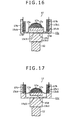
- FIG. 16 is a cross sectional view showing still another construction of the variable capacitor 15.
- FIG. 17 is a cross sectional view showing yet another construction of the variable capacitor 15.
- the variable capacitor 15 in the embodiment of the input device described above is described as being composed of the dielectric 15a, the ring-like spacer 15b, and the conductive elastic member 15c.
- FIGS. 15A and 15B to FIG. 17 portions having the same constructions as those of the variable capacitor 15 described mainly with reference to FIG. 3 to FIGS. 6A and 6B are designated by the same reference numerals or symbols, respectively, and detailed descriptions thereof are omitted here for the sake of simplicity.
- a variable capacitor 15(1) shown in FIGS. 15A and 15B is such that an insulator portion 15x is provided on the bottom surface of the holding hole 15ch for a board and the like of the holder portion 15cl for a board and the like instead of the ring-like spacer 15b.
- the insulator portion 15x is provided in a portion, indicated by slant lines, of the bottom surface of the holding hole 15ch for a board and the like.
- any of various kinds of insulators may be provided in the portion, indicated by the slant lines, of the bottom surface of the holding hole 15ch for a board and the like by carrying out evaporation, fusion, application or the like, or plural protrusions made of any suitable insulator may be provided in the portion, indicated by the slant lines, of the bottom surface of the holding hole 15ch for a board and the like, thereby making it possible to form the insulator portion 15x.
- the insulator portion 15x is formed on the bottom surface of the holding hole 15ch for a board and the like of the holder portion 15cl for a board and the like in such a way, which makes it unnecessary to accommodate the spacer 15b in the holding hole 15ch for a board and the like.
- a variable capacitor 15(2) shown in FIG. 16 is such that both of the lateral side portions 17d of the printed wiring board 17 are formed so as to protrude (downwardly in FIG. 16 ) relative to the dielectric 15a, which is firmly fixed to the bottom side portion of the printed wiring board 17 (via the solder 17x).
- the dielectric 15a firmly fixed to the bottom side portion of the printed wiring board 17 is spaced (above) from the bottom surface (the dielectric contacting portion 15cX) of the holding hole 15ch for a board and the like by both of the lateral side portions 17c of the printed wiring board 17.
- the space 15d can be provided between the second surface portion 15a2 of the dielectric 15a and the dielectric contacting portion 15cX.
- both of the printed wiring board 17 and the dielectric 15a are formed so as to have the same constructions as those of the corresponding portions of the embodiment described with reference to FIGS. 6A and 6B , and the like.
- the holding hole 15ch for a board and the like is formed so as to be different in shape from the corresponding portion of the embodiment described with reference to FIGS. 6A and 6B , and the like.
- each of the groove portions 15ck into which the printed wiring board 17 is fitted is made shallow.
- the dielectric 15a firmly fixed to the printed wiring board 17 is spaced (above) from the bottom surface (the dielectric contacting portion 15cX) of the holding hole 15ch for a board and the like.
- the space 15d can be provided between the second surface portion 15a2 of the dielectric 15a and the dielectric contacting portion 15cX.
- the second surface portion 15a2 of the dielectric 1a and the bottom surface (the dielectric contacting portion 15cX) of the holding hole 15ch for a board and the like are spaced from each other to provide the space 15d, thereby making it possible to make the use of the spacer 15b unnecessary.
- the spacer 15b it is preferable either to use the spacer 15b or to provide the insulator portion 15x. That is, it is preferable to construct the variable capacitor either like the variable capacitor 15 described with reference to FIG. 3 to FIGS. 6A and 6B , or like the variable capacitor 15(1) described with reference to FIGS. 15A and 15B .
- the portion of the printed wiring board 17 connected to the conductive elastic member 15c need not be constructed in the form of one sheet of board, but, for example, may be constructed as a combination of multiple boards that are crossed, thereby making it possible to provide the same state as that in the case where the spacer 15b is provided.
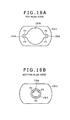
- FIGS. 18A and 18B are a top plan view and a bottom plan view, respectively, each showing another construction of the conductive elastic member 15c.
- FIGS. 19A and 19B are a top plan view and a transverse cross sectional view, respectively, each showing still another construction of the conductive elastic member 15c. It is noted that in FIGS. 18A and 18B and FIGS. 19A and 19B , portions which have the same constructions as those in the case of the variable capacitor 15 mainly described with reference FIG. 3 to FIGS. 6A and 6B are designated by the same reference numerals or symbols, respectively, and thus detailed descriptions thereof are omitted here for the sake of simplicity.
- a conductive elastic material 15c(1) shown in FIGS. 18A and 18B is basically formed in the same manner as that in the case of the conductive elastic material 15c described with reference to FIGS. 4A and 4B .
- each of the groove portions 15ck provided in positions facing each other of the outer periphery of the holding hole 15ch for a board and the like of the holder portion 15cl for a board and the like is different in shape from that shown in FIG. 4A .
- the core body holding hole 15cp of the core body holder portion 15c2 is also different in shape from that shown in FIG. 4B .
- paired protrusions P1 are provided in respective positions facing each other in each of the groove portions 15ck provided in the respective positions facing each other of the paired outer periphery of the holding hole 15ch for a board and the like.
- Each of the protrusions P1 is formed in rod-like shape so as to extend from the upper end to the lower end of the groove portion 15ck.
- a pair of protrusions P1 is provided such that, when the portions of the printed wiring board 17 having the second lead pieces 17b are inserted into the groove portions 15ck, respectively, each of the second lead piece 17b portions can be more firmly held between the paired protrusions P1. Therefore, the second lead pieces 17b and the conductive elastic member 15c(1) can be electrically connected more relatively. In addition, the printed wiring board 17 mounted to the conductive elastic member 15c(1) can be prevented from being detached from the conductive elastic member 15c(1).
- the core body holding hole 15cp is not provided with any of the slit portions 15cs, and instead, three protrusions P2 are provided inside the core body holding hole 15cp.
- Each of the three protrusions P2 is formed in rod-like shape so as to extend from the upper end to the lower end of the core body holding hole 15cp.
- the three protrusions P2 are provided such that the core body 12 inserted into the core body holding hole 15cp can be more firmly held by the three protrusions P2, and the core body 12 can be reliably held by the core body holding hole 15cp. In other words, the core body 12 can be prevented from being detached from the core body holding hole 15cp.
- a conductive elastic member 15c(2) shown in FIGS. 19A and 19B is composed of the holder portion 15c1 for a board and the like, and the core body holder portion 15c2 similarly to the case of the conductive elastic member 15c described above with reference to FIGS. 4A and 4B .
- the holder portion 15c1 for a board and the like is provided with the holding hole 15ch for a board and the like
- the core body holder portion 15c2 is provided with the core body holding hole 15cp.
- FIG. 19B is a cross sectional view of the conductive elastic member 15c(2) when viewed in the direction of an arrow "a" in FIG. 19A .
- the holding hole 15ch for a board and the like is provided inside the holder portion 15c1 for a board and the like.
- a construction is adopted such that the cover portions KU and KD are provided in the upper portion of the holder portion 15c1 for a board and the like so as to close the opening portion of the holding hole 15ch for a board and the like.
- FIG. 20 is a cross sectional view showing the other construction of the core body holder portion 15c2.
- the core body holder portion 15c2 of the embodiment described above has the cylindrical core body holding portion 15cp (refer to FIG. 3 ) in order to insert and hold the axis portion 12b of the core body 12 into the core body holder portion 15c2.
- the core body holder portion 15c2 may be damaged due to the shock in some cases.
- connection cap 20 is provided between the axis portion 12b of the core body 12 and the core body holder portion 15c2. Additional provision of the connection cap 20 results in that the core body holder portion 15c2 can be prevented from being damaged by the shock caused by dropping of the pen.
- variable capacitor 15 having the performance equal to that of the conventional variable capacitor can be realized by provision of the dielectric 15a, the spacer 15b, and the conductive elastic member 15c.
- variable capacitors 15(1), 15(2), 15(3), etc. each not using the spacer 15b.
- variable capacitor As a result, it is possible to realize a variable capacitor with a dramatically reduced number of parts or components, as compared with the case of the conventional variable capacitor. Therefore, it is possible to realize a variable capacitor, which has a reduced number of parts or components and which can be very simply manufactured. These effects make it possible to largely reduce the cost of the variable capacitor. It is also possible to realize a position indicator using the variable capacitor, and an input device using the position indicator, which are further useful in reducing the cost of the position indicator and the input device.
- the conductive elastic member 15c has been described as including both of the holder portion 15c1 for a board and the like, and the core body holder portion 15c2, the present invention is by no means limited thereto.
- the core body 12 is held movably in the axis direction within the first case 18 as shown in FIG. 2 by a mechanism provided in the first case 18 side, which ensures that the predetermined position of the conductive elastic member 15c is depressed by the core body 12, it is unnecessary to provide the core body holder portion 15c2.
- the shape of the holding hole 15ch for a board and the like of the holder portion 15c1 for a board and the like can be variously changed.
- the dielectric 15a can be formed in a polygonal columnar shape such as a quadrangular columnar shape
- the spacer 15b can also be formed in a polygonal columnar shape such as a quadrangular columnar shape so as to correspond to the shape of the dielectric 15a.
- the holding hole 15ch for a board and the like of the holder portion 15c1 1 for a board and the like has a polygonal opening portion, which agrees in shape with the shape of the dielectric 15a or the spacer 15b.
- variable capacitor 15 is constructed such that the second lead piece 17b of the printed wiring board 17 is normally in contact with the conductive elastic member 15c, while only when the core body 12 is depressed the dielectric contacting portion 15cX (of the conductive elastic member 15c) comes in contact with the second surface portion 15a2 of the dielectric 15a connected to the first lead piece 17a of the printed wiring board 17.
Landscapes
- Engineering & Computer Science (AREA)
- General Engineering & Computer Science (AREA)
- Theoretical Computer Science (AREA)
- Human Computer Interaction (AREA)
- Physics & Mathematics (AREA)
- General Physics & Mathematics (AREA)
- Power Engineering (AREA)
- Microelectronics & Electronic Packaging (AREA)
- Position Input By Displaying (AREA)
- Measurement Of Length, Angles, Or The Like Using Electric Or Magnetic Means (AREA)
- Switches That Are Operated By Magnetic Or Electric Fields (AREA)
Description
- The present invention relates to a variable capacitor whose capacitance value is changed in accordance with a pressure or a displacement applied thereto from the outside, a position indicator using the variable capacitance, and an input device using the position indicator.
- In recent years, an input device has been used with a personal computer and the like. The input device is composed, for example, of a position indicator and a position detector. In this case, the position indicator is formed as of a pen type. The position detector has an input surface to which a pointing operation, characters, figures and the like are inputted by using the position indicator.
- A variable capacitor as described in Japanese Patent Laid-Open No.
Hei 4-96212 Patent Document 1 includes a first electrode and a second electrode. The first electrode is mounted to one surface of a dielectric. The second electrode is disposed on the other surface of the dielectric and has flexibility. The variable capacitor includes a section for separating the second electrode and the other surface of the dielectric by a small space, except for a portion of the second electrode and the other surface of the dielectric, and a section for applying a relative pressure or displacement between the second electrode and the dielectric. -
FIGS. 21A and 21B are schematic views each showing a concrete construction of a conventional variable capacitor.FIG. 21A is a schematic view showing an initial state in the conventional variable capacitor, andFIG. 21B is a schematic view showing a state in which a pressure is applied to the conventional variable capacitor. - The
variable capacitor 200 includes a dielectric 201 having approximately a disc-like shape, afirst electrode 202, and asecond electrode 203. In this case, thefirst electrode 202 is mounted on onesurface 201 a of the dielectric 201. Thesecond electrode 203 is disposed on theother surface 201 b opposite to the onesurface 201a of the dielectric 201. Thesecond electrode 203 has flexibility and is disposed on theother surface 201b of the dielectric 201 through a ring-like spacer 204. In addition, a rod-like core body 210 is provided on a side of thesecond electrode 203 opposite to the dielectric 201 side through anelastic body 205. - A
first terminal 206 is provided on the one surface side of thefirst electrode 202. Thefirst terminal 206 is composed of a disc-like flange portion 206a, and alead portion 206b extending approximately from a center of one surface of the disc-like flange portion 206a. When a pen pressure is applied to thevariable capacitor 200, theflange portion 206a comes in contact with one surface of thefirst electrode 202 to be electrically connected to thefirst electrode 202. - A
second terminal 207 is provided in an end (edge) portion of thesecond electrode 203. Thesecond terminal 207 is composed of a disc-like flange portion 207a and alead portion 207b extending approximately from a center of one surface of theflange portion 207a similarly to the case of thefirst terminal 206. When the pen pressure is applied to thevariable capacitor 200, theflange portion 207a is in contact with an end portion of one surface of thesecond electrode 203 and is electrically connected to thefirst electrode 203. - In the
variable capacitor 200, in a state in which neither the pressure nor the displacement is applied to the core body 210 (initial state), a small space is defined between theother surface 201b of the dielectric 201 and thesecond electrode 203 by aspacer 204. As shown inFIG. 21B , when the pressure is applied to thecore body 210, both of theelastic body 205 and thesecond electrode 203 are depressed by thecore body 210 to be elastically deformed. As a result, thesecond electrode 203 comes in contact with theother surface 201b of the dielectric 201. When a contact area between thesecond electrode 203 and theother surface 201b of thedielectric 201 is increased, a value of an electrical capacitance defined between the first andsecond terminals second terminals core body 210. - The conventional
variable capacitor 200 described with reference toFIGS. 21A and 21B is actually formed within a housing member. Specifically, with respect to assembly of thevariable capacitor 200, as shown inFIG. 22 , the dielectric 201 having thefirst electrode 202 provided thereon, thespacer 204, thesecond electrode 203, and theelastic body 205 are laminated in this order to be formed within thehousing member 221. - In this case, the
first terminal 206 is connected to thefirst electrode 202, and thesecond terminal 207 is connected to the end (edge) portion of thesecond electrode 203. Also, both of acap body 72 for holding thecore body 210 and asecond housing member 222 are inserted from a lower side of thefirst housing member 221 into thefirst housing member 221, thereby forming onevariable capacitor 200. - Therefore, the conventional
variable capacitor 200 is formed from the nine parts or components: (1) thefirst terminal 206; (2) thesecond terminal 207; (3) thefirst housing member 221; (4) thedielectric 201 having thefirst electrode 202 provided thereon; (5) thespacer 204; (6) thesecond electrode 203; (7) theelastic body 205; (8) thecap body 72 for holding thecore body 210; and (9) thesecond housing member 222. - As described above, there are a large number of parts or components in the conventional
variable capacitor 200. In addition, the size of the conventionalvariable capacitor 200 is relatively small because the conventionalvariable capacitor 200 is accommodated in a pen-type position indicator. For this reason, it is rather difficult and time-consuming to manufacture the conventionalvariable capacitor 200 in some cases. - The invention relates to a variable capacitor according to
claim 1.Claims 2 to 15 refer to specifically advantageous realizations of the subject matter ofclaim 1. - In light of the foregoing, according to one aspect of the present invention, a variable capacitor is provided which is simpler to construct, without having its performance compromised. Further, a position indicator using such variable capacitor, and an input device including such position indicator are provided.
- According to an embodiment of the present invention, a variable capacitor is provided for use with an electronic circuit board including a first terminal portion and a second terminal portion, which are all to be built in a position indicator. The variable capacitor includes a dielectric having a first surface portion and a second surface portion opposite to said first surface portion, and a conductive elastic member having a board coupling portion and a dielectric contacting portion. The first terminal portion is coupled to the first surface portion, the second terminal portion is coupled to the board coupling portion, and the dielectric contacting portion is disposed separately from the second surface portion so as to face the second surface portion and is further configured to be deformed to come in contact with the second surface portion of the dielectric. A contact area between the second surface portion and the dielectric contacting portion is changed in correspondence to a depressing force, which is applied against the dielectric contacting portion in a direction toward the dielectric, thereby changing an electrostatic capacitance of the variable capacitor.
- In the variable capacitor described above, the first terminal portion of the electronic circuit board is coupled to the first surface portion of the dielectric, and the second terminal portion of the electronic circuit board is coupled to the board coupling portion of the conductive elastic member. The dielectric contacting portion of the conductive elastic member is disposed separately (spaced) from the second surface portion of the dielectric so as to face the second surface portion of the dielectric, but is configured to be deformed toward the second surface portion when a depressing force is applied. In other words, the dielectric contacting portion and the second surface portion of the dielectric come in contact with each other when the depressing force is applied. The contact area between the dielectric contacting portion and the second surface portion of the dielectric is changed, thereby changing the electrostatic capacitance of the variable capacitor.
- Therefore, when a depressing force is applied, a connection system is formed as follows: the first terminal portion of the electronic circuit board → the first surface portion of the dielectric → the second surface portion of the dielectric → the dielectric contacting portion of the conductive elastic member → the board coupling portion of the conductive elastic member → the second terminal portion of the electronic circuit board. In the connection system, the variable capacitor is provided whose electrical capacitance changes in accordance with the contact state, corresponding to the depressing force, between the second surface portion of the dielectric and the dielectric contacting portion of the conductive elastic member.
- As a result, a variable capacitor is provided, which has a very simple construction including two members: the dielectric and the conductive elastic member. In addition, the performance of the variable capacitor is not degraded as compared with that of a conventional variable capacitor. In other words, it is possible to realize a variable capacitor, which is simpler to construct and yet maintains high performance.
- According to another embodiment of the present invention, a position indicator is provided including the variable capacitor as described above, an electronic circuit board having electronic circuit provided therein, and a resonance circuit having the variable capacitor as its element.
- Therefore, it is possible to realize a position indicator using the variable capacitor, which is simpler to construct and maintains high performance.
- According to still another embodiment of the present invention, an input device is provided including a position indicator and a position detector having a detection surface configured to detect a position indicated by the position indicator. The position indicator includes a case, an elongated core body accommodated within the case and having one end thereof protruding from the case while having another end thereof accommodated within the case, a variable capacitor whose electrical capacitance changes when an external force is applied thereto through the core body, and an electronic circuit board having a first terminal portion and a second terminal portion. The variable capacitor of the position indicator includes a dielectric having a first surface portion and a second surface portion opposite to the first surface portion, and a conductive elastic member having a board coupling portion and a dielectric contacting portion. The first terminal portion is coupled to the first surface portion, the second terminal portion is coupled to the board coupling portion, and the dielectric contacting portion is disposed separately from the second surface portion so as to face the second surface portion and is configured to be deformed to come in contact with said second surface portion. A contact area between the second surface portion and the dielectric contacting portion is changed in correspondence to a depressing force, which is applied against the dielectric contacting portion in a direction toward the dielectric, thereby changing an electrostatic capacitance of the variable capacitor.
- Therefore, it is possible to realize an input device using the position indicator of the present invention.
- As set forth hereinabove, according to various embodiments of the present invention, it is possible to realize a variable capacitor which is simpler to construct and maintains high performance. In addition, it is possible to realize a position indicator using the variable capacitor, and an input device using such position indicator including the variable capacitor.
-
-
FIG. 1 is a perspective view showing a construction of an embodiment of an input device according to the present invention; -
FIG. 2 is a cross sectional view taken along line A-A' of a position indicator shown inFIG. 1 ; -
FIG. 3 is an exploded perspective view of a variable capacitor in the embodiment of the input device shown inFIG. 1 ; -
FIGS. 4A and 4B are a top plan view and a bottom plan view, respectively, of a conductive elastic member of the variable capacitor shown inFIG. 3 ; -
FIG. 5 is a cross sectional view of the variable capacitor portion when both of a printed wiring board and a core body are mounted; -
FIGS. 6A and 6B are cross sectional views explaining an example of joining between a printed wiring board and a dielectric; -
FIG. 7 is a graph representing pen pressure characteristics of the variable capacitor; -
FIG. 8 is a block diagram, partly in circuit, showing a position indicator and a position detector composing the input device according to an embodiment of the present invention; -
FIG. 9 is a flow chart showing processing executed by a processing portion of the position detector composing the input device according to an embodiment of the present invention; -
FIGS. 10A to 10D are waveform charts respectively showing waveforms obtained in different portions, in an X-axis global scanning operation carried out by the position detector composing the input device according to an embodiment of the present invention; -
FIGS. 11A to 11D are waveform charts respectively showing waveforms obtained in different portions, in a Y-axis global scanning operation carried out by the position detector composing the input device according to an embodiment of the present invention; -
FIGS. 12A to 12D are waveform charts respectively showing waveforms obtained in different portions, in an X-axis sector scanning operation and a Y-axis sector scanning operation carried out by the position detector composing the input device according to an embodiment of the present invention; -
FIG. 13 is a circuit diagram showing another configuration of a resonance circuit provided in the position detector composing the input device according to an embodiment of the present invention; -
FIG. 14 is a circuit diagram showing another configuration of the position detector composing the input device according to an embodiment of the present invention; -
FIGS. 15A and 15B are a cross sectional view showing another construction of the variable capacitor, and a top plan view showing a construction of a conductive elastic portion shown inFIG. 15A , respectively; -
FIG. 16 is a cross sectional view showing still another construction of the variable capacitor; -
FIG. 17 is a cross sectional view showing yet another construction of the variable capacitor; -
FIGS. 18A and 18B are a top plan view and a bottom plan view, respectively, each showing another construction of the conductive elastic member; -
FIGS. 19A and 19B are a top plan view and a transverse cross sectional view, respectively, showing still another construction of the conductive elastic member; -
FIG. 20 is a cross sectional view showing another construction of a core body holder portion; -
FIGS. 21A and 21B are an explanatory view schematically showing an initial state of a conventional variable capacitor, and an explanatory view showing a state in which a pressure (pen pressure) is applied to a core body of the conventional variable capacitor, respectively; and -
FIG. 22 is an exploded perspective view showing a concrete construction of the conventional variable capacitor shown inFIGS. 21A and 21B . - The preferred embodiments of the present invention will be described in detail hereinafter with reference to the accompanying drawings. It is noted that members common to the figures are designated by the same reference numerals or symbols, respectively. In an embodiment which will be described below, an accommodating portion claimed in the appended claims is embodied as a holding hole 15ch for a board and the like. A board coupling portion claimed in the appended claims is embodied as a groove portion 15ck provided in a holder portion 15cl for a board and the like in one embodiment. Also, a core coupling portion claimed in the appended claims is embodied as a core body holding hole 15cp and a core body holder 15c2 in one embodiment.
- Firstly, a schematic construction of an embodiment of the input device according to the present invention will be described with reference to
FIG. 1. FIG. 1 is a perspective view showing the schematic construction of the embodiment of the input device according to the present invention. - The
input device 10 is composed of aposition detector 1, and aposition indicator 2 for inputting information to theposition detector 1. - The
position detector 1 is connected to an external apparatus such as a personal computer or a Personal Digital Assistant (PDA) via acable 8, whereby theposition detector 1 is used as an input device for such an external apparatus. It is noted that although not specifically illustrated, such aposition detector 1 may be built in the personal computer or the like. - The
position detector 1 is composed of a detectingportion 4 and achassis 5. In this case, the detectingportion 4 detects a position indicated by theposition indicator 2, which will be described later. Thechassis 5 forms approximately a hollow thin rectangular parallelepiped and has the detectingportion 4. Thechassis 5 has anupper chassis 7 and a lower chassis (not shown). In this case, theupper chassis 7 has an opening portion 6 for exposing a detection surface of the detectingportion 4. Theupper chassis 7 is superposed on the lower chassis (not shown). The detectingportion 4 is fitted into the quadrangular opening portion 6 of theupper chassis 7, so that the input surface of the detectingportion 4 is exposed through the quadrangular opening portion 6. Theposition detector 1 having such a construction receives an input of characters, figures or the like, made by a pointing operation of theposition indicator 2, which will be described below. - Next, a description will be given with respect to a schematic construction of the
position indicator 2 with reference toFIG. 2. FIG. 2 is a cross sectional view taken along line A-A' of theposition indicator 2 shown inFIG. 1 . - The
position indicator 2 serves to indicate a position for theposition detector 1 by using an electromagnetic induction system. Theposition indicator 2 has a resonance circuit which enters into resonance with an electric wave having a specific frequency and transmitted thereto from theposition detector 1. Theposition indicator 2 transmits a resonance signal detected by the resonance circuit to theposition detector 1, thereby indicating a position for theposition detector 1. - As shown in
FIG. 2 , theposition indicator 2 is constructed so as to include acase 11 showing a concrete example of a chassis, acore body 12, aposition indicating coil 13, avariable capacitor 15, aferrite core 16, and a printedwiring board 17. - The
case 11 is formed as an external packaging portion of theposition indicator 2. Thecase 11 has a bottomed cylindrical shape whose one end is closed. Thecase 11 is composed of afirst case 18 and asecond case 19 which are assembled, and coupled with thefirst case 18 and thesecond case 19 being axially superposed on each other. Thefirst case 18 has approximately a conical shape at one end side in an axial direction, and has anopening portion 18a at a tip of that one end side. The other end of thefirst case 18 in the axial direction is open. - The
second case 19 has a cylindrical shape whose one end in the axial direction is open and whose other end is closed. Thefirst case 18 and thesecond case 19 are disposed on the same axis line, and are fixed to each other by using a firmly fixing section such as an adhesive agent or fixing screws. The printedwiring board 17 having electronic parts or components mounted thereto is firmly fixed to thesecond case 19 by using a firmly fixing section such as an adhesive agent or fixing screws. Theferrite core 16 is accommodated in thefirst case 18. - The
ferrite core 16, for example, has a cylindrical shape, and acore body 12 is inserted into acylindrical hole 16a of theferrite core 16. Anindication portion 12a of thecore body 12 protrudes from one end side in the axial direction of theferrite core 16. In addition, aposition indicating coil 13 composing a resonance circuit is wound around the outer periphery of theferrite core 16 to be mounted thereto. Both ends (not shown) of theposition indicating coil 13 are electrically connected to opposite terminals of corresponding one of the electronic parts or components firmly fixed to the printedwiring board 17, respectively. Electronic parts or components composing the resonance circuit are mounted to the printedwiring board 17. - The
core body 12 is made from approximately a rod-like member, and is accommodated in thecase 11 along the axial direction of thecase 11. Thecore body 12 is composed of theindication portion 12a, and anaxis portion 12b. In this case, theindication portion 12a has a role of a pen tip at one end of thecore body 12 in the axial direction. Theaxis portion 12b is continuously formed from theindication portion 12a. Theindication portion 12a is formed approximately in a conical shape. Theindication portion 12a protrudes from theopening portion 18a of thefirst case 18 toward the outside when thecore body 12 is accommodated in thecase 11. Thevariable capacitor 15 is mounted to the other end of theaxis portion 12b in the axial direction. - Next, the
variable capacitor 15 of theposition detector 1 composing an embodiment of the input device will be described with reference toFIG. 3 to FIGS. 6A and6B .FIG. 3 is an exploded perspective view of thevariable capacitor 15.FIGS. 4A and 4B are a top plan view and a bottom plan view, respectively, of a conductiveelastic member 15c of thevariable capacitor 15. In addition,FIG. 5 is a cross sectional view of thevariable capacitor 15 portion when both of the printedwiring board 17 and thecore body 12 are mounted to thevariable capacitor 15. Also,FIGS. 6A and 6B are cross sectional views explaining an example of joining between the printedwiring board 17 and a dielectric 15a. - The
variable capacitor 15 is a capacitor whose capacitance value is changed so as to correspond to a pressure (pen pressure) applied to theposition indicator 2. Thevariable capacitor 15 detects the pen pressure applied to thecore body 12 as a corresponding change in capacitance value, and thus serves as a pen pressure detecting portion of theposition indicator 2. - As shown in
FIG. 3 , thevariable capacitor 15 is composed of the dielectric 15a, a spacer (spacing member) 15b, and the conductiveelastic member 15c. The dielectric 15a, the space (spacing member) 15b, and the conductiveelastic member 15c are held between the printedwiring board 17 and thecore body 12, to be used as thevariable capacitor 15 of theposition indicator 2. - The dielectric 15a is formed in a columnar shape having a first surface portion 15a1 and a second surface portion 15a2 opposite to each other. In the illustrated embodiment, for example, the dielectric 15a is 2.95 mm in outer diameter, 1 mm in thickness, and 160 pF (permittivity: 4,000 F/m) in capacitance value. Here, the unit, mm, means a millimeter, the unit, pF, means a picofarad, and the unit, F/m, means a meter per farad.
- It is noted that numerical values of the dielectric 15a provided above are examples only, and thus various numerical values can be adopted in accordance with the size of the
position indicator 2 having thevariable capacitor 15 mounted thereto, the size of the printedwiring board 17, and the like. In one embodiment, the second surface portion 15a2 of the dielectric 15a is subjected to mirror polishing, thereby increasing the degree of adhesion to a dielectric contacting portion 15cX of the conductiveelastic member 15c (seeFIG. 5 ), which will be described later. In addition, various kinds of materials such as ceramics and plastic can be used as the material for the dielectric 15a as long as they meet the conditions of the capacitance, the permittivity, and the like. - The spacer (spacing member) 15b is formed in a ring-like (annular) shape. An inner diameter of the
spacer 15b is smaller than a diameter of the dielectric 15a and an outer diameter of thespacer 15b is larger than the diameter of the dielectric 15a and is slightly smaller than an inner diameter of the conductiveelastic member 15c, which will be described later, into which the spacer is accommodated. Adoption of such a construction can prevent position shift of thespacer 15b within the conductiveelastic member 15c. - When the
spacer 15b is made to correspond to the dielectric 15a having the size exemplified above, thespacer 15b is set to be about 2.6 mm in inner diameter, and about 4.3 mm in outer diameter. In addition, the thickness of thespacer 15b is set equal to or smaller than 125 µm, for example. Of course, the numerical values shown here are examples only, and thus suitable material values can be adopted based on the size and the like of the dielectric 15 a. In addition, although various kinds of insulators can be used as the material for thespacer 15b, thespacer 15b may be formed from a Polyethylene Terephthalate (PET) film or a polyimide film, for example. - A holder portion 15cl for a board and the like, and the core body holder portion 15c2, are formed integrally with each other, by using a conductive rubber, into the conductive
elastic member 15c. - The holder portion 15c1 for a board and the like is a cylindrical portion which has an opening portion having a diameter slightly larger than the outer diameter of the
spacer 15b, and which is provided with a holding hole (accommodating portion) 15ch for a board and the like having a predetermined depth while maintaining an area of the opening portion. Thespacer 15b, the dielectric 15a, and a terminal portion of the printedwiring board 17 are accommodated in order from the lower side in the holding hole 15ch for a board and the like to be held therein. It is noted that a side of the holder portion 15c1 for a board and the like opposite to the opening portion thereof is provided with a closed bottom surface. This bottom surface composes the dielectric contacting portion 15cX, which is configured to contact the second surface portion 15a2 of the dielectric 15a (seeFIG. 5 ). - In addition, as shown in
FIG. 3 , a paired groove portions 15ck composing a board coupling portion are provided in respective positions facing each other of the outer periphery of the holding hole 15ch for a board and the like of the holder portion 15c1 for a board and the like. That is to say, as shown in a top plan view of the conductiveelastic member 15c ofFIG. 4A , a construction is adopted such that the paired groove portions 15ck composing the board coupling portion into which the printedwiring board 17 is inserted are provided in the respective positions facing each other of the opening portion of the holding hole 15ch for a board and the like of the holder portion 15cl for a board and the like. - A depth of each of the paired groove portions 15ck is set slightly shallower (shorter) than that of the holding hole 15ch for a board and the like (see
FIG. 5 ). In addition, a width, w, of each of the paired groove portions 15ck shown inFIG. 4A is set slightly narrower than a thickness of the printedwiring board 17 inserted into the paired grooves 15ck. As a result, the printedwiring board 17 inserted into the paired grooves 15ck is held by the paired grooves 15ck, and the printedwiring board 17 is prevented from being easily detached from the holder portion 15cl for a board and the like of the conductiveelastic member 15c. Also, although details will be described later, a lead piece (terminal portion) provided in the printedwiring board 17 and the conductiveelastic member 15c can be electrically connected to each other. - In addition, the holder portion 15cl for a board and the like has a shape as shown in
FIG. 4A , in which outer peripheral portions in a direction (in a vertical direction inFIG. 4A ) intersecting with a diameter direction connecting the paired groove portions 15ck are cut away. Adoption of such a shape results in that the conductiveelastic member 15c, which is hard to roll and is easy to handle, can be formed without wastefully using a conductive rubber. - On the other hand, the core body holder 15c2 is provided in such a way that a (closed) bottom surface thereof is flush with the bottom surface of the holder portion 15cl for a board and the like. The core body holder portion 15c2 is provided in such a way that an outer diameter thereof is smaller than that of the holder portion 15c1 for a board and the like, and a center of the bottom surface of the holder portion 15c1 for a board and the like, and a center of the bottom surface of the core body holder 15c2 agree with each other.
- The core body holder 15c2 is a cylindrical portion which has an opening portion having a diameter slightly smaller than an outer diameter of the
axis portion 12b of thecore body 12 and which is provided with a core body holding hole (core body coupling portion) 15cp having a predetermined depth while maintaining an area of the opening portion. As shown inFIG. 3 , theaxis portion 12b of thecore body 12 is inserted into the core body holding hole 15cp to be held. - In addition, as shown in the bottom plan view of the conductive
elastic member 15c ofFIG. 4B , a construction is adopted such that paired slit portions (cut portions) 15cs are provided in respective positions facing each other of the opening portion of the core body holding hole 15cp of the core body holder portion 15c2. A depth of each of the paired slit portions 15cs is set slightly shallower (shorter) than that of the core body holding hole 15cp. Provision of the paired slit portions 15cs results in that it is easy to insert thecore body 12 into the core body holding hole 15cp. - It is noted that the conductive rubber composing the conductive
elastic member 15c is a synthetic rubber with which a conductive particle such as a carbon particle or a silver particle is mixed, and is a material having the flexibility and the elasticity as well as the conductivity. In general, conductive rubber is classified into one of two types: a rubber of a type in which an electrical resistance value depends on a pressure, that is, a rubber (pressure-sensitive rubber) of a type having a tendency such that a resistance value becomes small as a depressing force applied is larger, and a rubber (narrow conductive rubber) of a type in which an electrical resistance value does not depend on a pressure. Any of the two types of rubbers can be used as the material composing the conductiveelastic member 15c. - Although the phrases such as flexibility and elasticity are the terms which are normally used interchangeably with each other, these phrases can be defined as follows. Flexibility is a property capable of being bent, or a property capable of being pliant. Thus, flexibility means that a material can be deformed when a depressing force is applied thereto, and can be restored back to the original state when the depressing force is removed. In this case, whether or not a size of the material itself is changed with respect to (along) the depressing direction is not relevant. On the other hand, elasticity means that a size of a material itself is reduced along a depressing direction when a depressing force is applied to the material, and the material can be returned back to the original state when the depressing force is removed. In this case, whether or not the material itself is bent with respect to the depressing direction is not relevant. Therefore, the conductive
elastic member 15c (having flexibility) in the embodiment can be bent or contracted when the pressure is applied thereto and can be restored back to the original state when the pressure is removed. - As described above with reference to
FIG. 3 , in thevariable capacitor 15 in the embodiment of the input device, both of the dielectric 15a and thespacer 15b are accommodated in the holding hole 15ch for a board and the like provided in the holder portion 15cl for a board and the like of the conductiveelastic member 15c. Also, the dielectric 15a, thespacer 15b, and the conductiveelastic member 15c are held between the printedwiring board 17 and thecore body 12, thereby serving as thevariable capacitor 15 of theposition indicator 2. - In an end portion of the printed
wiring board 17, connected to (or received within) thevariable capacitor 15 as shown inFIGS. 3 and5 , each of the two lateral side portions of the end portion is set slightly longer than a bottom side portion held between the two lateral side portions of the end portion. As further shown inFIGS. 3 and5 , a first lead piece (first terminal portion) 17a is provided in the bottom side portion of the printedwiring board 17, and second lead portions (second terminal portions) 17b are provided in both of the lateral side portions, respectively. The firstterminal portion 17a and the secondterminal portions 17b are connected to a predetermined circuit portion(s) provided on the printedwiring board 17 through respective lead lines (not shown). - The
first lead piece 17a of the printedwiring board 17 is electrically connected to the first surface portion 15al of the dielectric 15a, and the dielectric 15a itself is firmly fixed to the printedwiring board 17. In this case, thefirst lead piece 17a of the printedwiring board 17 and the first surface portion 15al of the dielectric 15a are joined to each other by, for example, using a method such as a soldering method or a brazing method. As a result, thefirst lead piece 17a of the printedwiring board 17, and the first surface portion 15al of the dielectric 15a are electrically connected to each other, and the dielectric 15a is firmly fixed to the printedwiring board 17. - It is noted that the soldering method or the brazing method is an example of the firmly fixing method. Thus, the
first lead piece 17a, and the first surface portion 15al of the dielectric 15a may be electrically connected to each other by using any of various kinds of conductive adhesive agents, and thus the dielectric 15a may be firmly fixed to the printedwiring board 17. - Both of the end portions of the lateral sides of the printed
wiring board 17 are respectively fitted into the paired groove portions (board coupling portions) facing each other and provided in the outer peripheral portion of the holding hole 15ch for a board and the like of the holder portion 15c1 for a board and the like of the conductiveelastic member 15c. As a result, as also described above, thesecond lead pieces 17b provided in both of the lateral side portions of the printedwiring board 17, respectively, are electrically connected to the conductiveelastic member 15c. - Specifically, as shown in a cross sectional view of the
variable capacitor 15 portion ofFIG. 5 , the ring-like spacer 15b is accommodated in the holding hole 15ch for a board and the like provided in the holder portion 15cl for a board and the like of the conductiveelastic member 15c so as to contact the bottom surface of the holding hole 15ch for a board and the like. Above the ring-like spacer 15b, the first surface portion 15al is electrically connected to thefirst lead piece 17a of the printedwiring board 17, and also the dielectric 15a firmly fixed to the printedwiring board 17 is accommodated together with the printedwiring board 17 from the opening portion of the holding hole 15ch for a board and the like. - In this case, both of the lateral side portions provided with the
second lead pieces 17b of the printedwiring board 17, respectively, are fitted into the paired groove portions (board coupling portions) 15ck facing each other and provided in the outer peripheral portion of the holding hole 15ch for a board and the like. As a result, thesecond lead pieces 17b provided in both of the lateral side portions of the printedwiring board 17, respectively, are electrically connected to the conductiveelastic member 15c through the respective groove portions 15ck composing the board coupling portions. - In this case, as shown in
FIG. 5 , the bottom surface portion of the holding hole 15ch for a board and the like of the holder portion 15c1 for a board and the like composing the dielectric contacting portion 15cX, and the second surface portion 15a2 of the dielectric 15a are separated (spaced) from each other by a thickness of thespacer 15b by thespacer 15b. That is to say, aspace 15d is defined between the bottom surface portion of the holding hole 15ch for a board and the like of the holder portion 15cl for a board and the like composing the dielectric contacting portion 15cX, and the second surface portion 15a2 of the dielectric 15a by thespacer 15b. - As shown in
FIG. 5 , theaxis portion 12b of thecore body 12 is fitted into the core body holding hole 15cp of the core body holder portion 15c2 of the conductiveelastic member 15c. It is then supposed that a depressing force is applied to the dielectric 15a side of thecore body 12 when, for example, theindication portion 12a of thecore body 12 is pressed against the detectingportion 4 of theposition detector 1. - In this case, the conductive
elastic member 15c has elasticity and flexibility as well as conductivity. Therefore, the bottom surface portion (the dielectric contacting portion 15cX) of the holding hole 15ch for a board and the like of the board holder portion 15cl is upward pressed toward the second surface portion 15a2 side of the dielectric 15a by thecore body 12. Also, the application of the depressing force toward the dielectric 15a by thecore body 12 results in that the bottom surface portion (the dielectric contacting portion 15cX) of the holding hole 15ch for a board and the like comes in contact with the second surface portion 15a2 of the dielectric 15a. - When the depressing force applied toward the dielectric 15a side of the
core body 12 is released, the conductiveelastic member 15c is returned back to the original state by the elasticity and flexibility of the conductiveelastic member 15c. As a result, the operation state is returned back to the state such that thespace 15d is defined between the bottom surface portion (the dielectric contacting portion 15cX) of the holding hole 15ch for a board and the like, and the second surface portion 15a2 of the dielectric 15a by thespacer 15b. - When the depressing force is not applied to the dielectric 15a side by the
core body 12 in such a way, thespace 15d is defined between the bottom surface portion (the dielectric contacting portion 15cX) of the holding hole 15ch for a board and the like, and the second surface portion 15a2 of the dielectric 15a, and therefore electrical connection is not formed. - However, when the depressing force is applied to the dielectric 15a side by the
core body 12, the bottom surface portion (the dielectric contacting portion 15cX) of the holding hole 15ch for a board and the like, and the second surface portion 15a2 of the dielectric 15a come in contact with each other. In this case, there is formed a connection system as follows: thefirst lead piece 17a of the printedwiring board 17 → the first surface portion 15al of the dielectric 15a → the second surface portion 15a2 of the dielectric 15a → the dielectric contacting portion 15cX of the conductiveelastic member 15c → the board coupling portion 15ck of the conductiveelastic member 15c → the secondterminal portion 17b of the printedwiring board 17. Thus, thevariable capacitor 15 is constructed whose electrical capacitance is changed in accordance with the contact state, corresponding to the depressing force, between the second surface portion 15a2 of the dielectric 15a, and the dielectric connecting portion 15cX of the conductiveelastic portion 15c in the connection system. - As shown in
FIGS. 3 and5 , thevariable capacitor 15 in the illustrated embodiment can be basically composed of the three parts or components: the dielectric 15a; thespacer 15b; and the conductiveelastic member 15c. Thevariable capacitor 15 having a very simple construction can be realized in this manner. - It has been described above that the
first lead piece 17a of the printedwiring board 17, and the first surface portion 15al of the dielectric 15a are joined to each other by, for example, using the soldering method. In thevariable capacitor 15 of the embodiment, for the purpose of reliably and firmly fixing the printedwiring board 17 to the first surface portion 15a1 of the dielectric 15a, a sample construction of a connection end of the printedwiring board 17 to (be connected to) the conductiveelastic member 15c is provided and now described. - In the embodiment as shown in
FIG. 6A , a semi-circular through hole (a cutout portion (or a holding hole) for holding the solder as the conductive adhesive agent) 17c is provided in thefirst lead piece 17a portion of the connection end of the printedwiring board 17, to be connected to the conductiveelastic member 15c. In other words, the bottom side portion of the printedwiring board 17 is cut into the semi-circular shape to provide the throughhole 17c. As shown inFIG. 6A , thefirst lead piece 17a is provided so as to have an arc-like shape along the outer peripheral portion of the semi-circular throughhole 17c. - As shown in
FIG. 6B , the first surface portion 15al of the dielectric 15a is made to come in contact with the throughhole 17c portion of the printedwiring board 17 constructed in such a way, and asolder 17x as the conductive adhesive agent is caused to flow into the throughhole 17c portion, thereby carrying out the soldering. As a result, as shown inFIG. 6B , the throughhole 17c is filled with thesolder 17x. Also, when thesolder 17x portion is solidified, the first surface portion 15al of the dielectric 15a, and thefirst lead piece 17a of the printedwiring board 17 are electrically connected to each other and also the dielectric 15a is firmly fixed to the printedwiring board 17. - Thus, in the illustrated embodiment, the construction is adopted such that the through
hole 17c is provided in the connection end of the printedwiring board 17 to be connected to the conductiveelastic member 15c, and the arc-like lead piece 17a is provided in the outer peripheral portion of the throughhole 17c. As a result, thefirst lead piece 17a of the printedwiring board 17 and the first surface portion 15al of the dielectric 15a can be electrically connected to each other and also the dielectric 15a can be firmly fixed to the printedwiring board 17. - It is noted that although the through
hole 17c has been described as being semi-circular here, the present invention is by no means limited thereto. For example, a through hole having a polygonal shape such as a triangular shape or a quadrangular shape may be provided, and the first lead piece may be provided in an outer periphery or edge of the through hole. - As described above, the
variable capacitor 15 composes the pen pressure detecting portion in theposition indicator 2. Next, a description will be given regarding the precision in detection of the pen pressure (pressure) by thevariable capacitor 15 of the embodiment described above. -
FIG. 7 is a graph showing phase-load characteristics of thevariable capacitor 15 with a load applied to thecore body 12 on an axis of abscissa, and a phase (a difference in phase between a transmitted electric wave and a received electric wave) on an axis of ordinate. - Although the
variable capacitor 15 of the embodiment described above has a very simple construction, as shown inFIG. 7 , thevariable capacitor 15 can detect a load (pressure) of about 10g. Also, thevariable capacitor 15 can approximately linearly detect the applied load up to about 100 g with high sensitivity. The applied load above 100 g up to about 300 g can be suitably detected as well. Although a change in phase difference against the applied load of 300 g or more becomes small, since application of a large pen pressure of 300 g or more to theposition indicator 2 is rare, practical utility of theposition indicator 2 using thevariable capacitor 15 is not compromised at all. - The phase-load characteristics of the
variable capacitor 15 shown inFIG. 7 are approximately the same as the characteristics of the position indicator using the conventional variable capacitor described with reference toFIGS. 21A and 21B , andFIG. 22 , for example. Therefore, although thevariable capacitor 15 of the illustrated embodiment is simple in construction, thevariable capacitor 15 maintains the same performance as compared with the conventional variable capacitor. - Next, a description will be given of a concrete circuit configuration of the
position detector 1, for detecting the indicated position and the pen pressure, by using theposition indicator 2 including thevariable capacitor 15 described above with reference toFIG. 8. FIG. 8 is a block diagram, partly in circuit, showing theposition indicator 2 and theposition detector 1. The input device is composed of theposition indicator 2 and theposition detector 1. - The
position indicator 2 is configured by aresonance circuit 61 composed of theposition indicating coil 13, thevariable capacitor 15 connected in parallel with theposition indicating coil 13, and aresonance capacitor 60a connected in parallel with thevariable capacitor 15 in terms of a circuit configuration. In various embodiments, theresonance circuit 61 changes its resonance frequency in accordance with a change in electrical capacitance of thevariable capacitor 15, and the change in resonance frequency is detected as a pen pressure. - On the other hand, in the
position detector 1, an X-axis directionloop coil group 104a, and a Y-axis directionloop coil group 104b are laminated and provided, thereby forming aposition detecting coil 101. Each of the X-axis directionloop coil group 104a, and the Y-axis directionloop coil group 104b is composed of 40 rectangular loop coils, for example. The rectangular loop coils composing each of the X-axis directionloop coil group 104a and the Y-axis directionloop coil group 104b are disposed in such a way that they are arranged at equal intervals to be superposed one upon another. - The
position detector 1 is provided with a selectingcircuit 106, to which both of the X-axis directionloop coil group 104a and the Y-axis directionloop coil group 104b are connected. The selectingcircuit 106 successively selects one loop coil from the X-axis directionloop coil group 104a and the Y-axis directionloop coil group 104b. - The
position detector 1 is provided with anoscillator 103, acurrent driver 105, aswitchover connecting circuit 107, a receivingamplifier 108, adetector 109, a low-pass filter 110, a sample-and-hold circuit 112, an A/D conversion circuit 113, asynchronous detector 116, a low-pass filter 117, a sample-and-hold circuit 118, an A/D conversion circuit 119, and aprocessing portion 114. - The
oscillator 103 is one which generates an A.C. signal having a frequency, f0, and supplies the resulting A.C. signal to each of thecurrent driver 105 and thesynchronous detector 116. Thecurrent driver 105 converts the A.C. signal supplied thereto from theoscillator 103 into an A.C. current, and sends the resulting A.C. current to theswitchover connecting circuit 107. Theswitchover connecting circuit 107 switches connection destinations (a transmission side terminal T and a reception side terminal R), to which the loop coil selected by the selectingcircuit 106 is connected in accordance with the control made by theprocessing portion 114, which will be described later. Of the connection destinations, thecurrent driver 105 is connected to the transmission side terminal T, and thereception amplifier 108 is connected to the reception side terminal R. - An induced voltage generated in the loop coil selected by the selecting
circuit 106 is sent to thereception amplifier 108 through the selectingcircuit 106 and theswitchover connecting circuit 107. Thereception amplifier 108 amplifies the induced voltage supplied thereto from the selected loop coil, and sends the induced voltage thus amplified to each of thedetector 109 and thesynchronous detector 116. - The
detector 109 detects the induced voltage generated in the selected loop coil, that is, the received signal, and sends the received signal thus detected to the low-pass filter 110. The low-pass filter 110 has a sufficient lower cutoff frequency than the frequency, f0, described above, converts the output signal from thedetector 109 into a D.C. signal, and sends the resulting D.C. signal to the sample-and-hold circuit 112. The sample-and-hold circuit 112 holds an analog voltage value at a predetermined timing of the output signal from the low-pass filter 110, specifically, at a predetermined timing during a period of time for reception, and sends the analog voltage to the Analog-to-Digital (A/D)conversion circuit 113. The A/D conversion circuit 113 converts the analog output from the sample-and-hold circuit 112 into a digital signal, and outputs the resulting digital signal to theprocessing portion 114. - On the other hand, the
synchronous detector 116 detects the output signal from thereception amplifier 108 synchronously with the A.C. signal from theoscillator 103, and sends a signal having a level corresponding to a difference in phase between the output signal and the A.C. signal to the low-pass filter 117. The low-pass filter 117 has a sufficiently lower cutoff frequency than the frequency, f0, and converts the output signal from thesynchronous detector 116 into a D.C. signal and sends the resulting D.C. signal to the sample-and-hold circuit 118. The sample-and-hold circuit 118 holds an analog voltage value at a predetermined timing of the output signal from the low-pass filter 117, and sends the analog voltage to the Analog-to-Digital (A/D)conversion circuit 119. The A/D conversion circuit 119 converts the analog voltage from the sample-and-hold circuit 118 into a digital signal, and outputs the resulting digital signal to theprocessing portion 114. - The
processing portion 114 controls the operations of the portions in theposition detector 1. In other words, theprocessing portion 114 controls the selection of the loop coil in the selectingcircuit 106, the switchover of theswitchover connecting circuit 107, and the timings of the sample-and-hold circuits processing portion 114 causes the X-axisdirection loop group 104a and the Y-axisdirection loop group 104b to transmit the electric wave for a given transmission duration in accordance with the input signals from the A/D conversion circuits - The induced voltage is generated in each of the loop coils of the X-axis
direction loop group 104a and the Y-axisdirection loop group 104b based on the electric wave transmitted from theposition indicator 2. Theprocessing portion 114 calculates the coordinate values of the indicated position in the X-axis direction and in the Y-axis direction in accordance with the level of the voltage value of the induced voltage generated in corresponding one of the loop coils. In addition, theprocessing portion 114 detects the pen pressure in accordance with the difference in phase between the transmitted electric wave and the received electric wave. - Next, an operation of the
position detector 1 carried out along a flow of processing in theprocessing portion 114 will be described with reference toFIG. 9. FIG. 9 is a flow chart representing the flow of the processing in theprocessing portion 114. - Firstly, the
processing portion 114 successively scans and selects the loop coils of the X-axisdirection loop group 104a (hereinafter, this successive scan and selection will be referred to as "global scan") (Step S1). - Concretely describing the global scan, the
processing portion 114 firstly sends information, in accordance with which the first loop coil of the X-axis directionloop coil group 104a, for example the loop coil X1, is selected by the selectingcircuit 106, and also sends a signal, in accordance with which the transmission side is selected by theswitchover connecting circuit 107. As a result, a sine wave signal having the frequency f0 is supplied from theoscillator 103 to the loop coil X1, so that the loop coil X1 generates the electric wave having the frequency, f0. At this time, when theposition indicator 2 either approaches or contacts the upper surface of the detectingportion 4 of theposition detector 1, the electric wave generated from the loop coil X1 excites theresonance circuit 61 having theposition indicating coil 13. As a result, the induced voltage having the frequency f0 is generated in theresonance circuit 61. - After the
processing portion 114 sends a signal, in accordance with which the transmission side terminal T is selected by theswitchover connecting circuit 107 for a given period of time, theprocessing portion 114 sends a signal, in accordance with which the reception side terminal R is selected by theswitchover connecting circuit 107, thereby causing the electric wave generated from the loop coil X1 to disappear. In this case, the induced voltage generated in theresonance circuit 61 of theposition indicator 2 having theresonance capacitor 60a and thevariable capacitor 15 gradually attenuates correspondingly, so that theresonance circuit 61 transmits the electric wave. The electric wave reversely excites the loop coil X1 described above, thereby causing the loop coil X1 to generate the induced voltage. - After the
processing portion 114 sends a signal, in accordance with which the reception side terminal R is selected by theswitchover connecting circuit 107 for a given period of time, theprocessing portion 114 sends information, in accordance with which the selectingcircuit 106 is caused to select the second loop coil from the X-axisdirection loop group 104a, for example the loop coil X2, to be connected to theswitchover connecting circuit 107. After that, theprocessing portion 114 sends a signal, in accordance with which the transmission side terminal T is selected by theswitchover connecting circuit 107, thereby carrying out the same transmission and reception of the electric wave as those in the foregoing. - After that, the
processing portion 114 executes the same processing as that of the foregoing, whereby the loop coils from the third to 40-th loop coils of the X-axis directionloop coil group 104a, for example the loop coils X3 to X40, are successively scanned and selected. As a result, the transmission and reception of the electric wave are carried out in the loop coils X3 to X40 in order. - It is noted that in the processing in Step S1, the
processing portion 114 may suitably limit the loop coils to be selected such as every other loop coil or one in every two loop coils. In addition, the transmission and reception of the electric wave for one loop coil may be carried out plural times. Moreover, although the transmission time for each of the loop coils need to be the same, and the reception time for each of the loop coils need to be the same, the transmission time and the reception time need not be identical to each other. - The induced voltage generated in the loop coil of the X-axis direction
loop coil group 104a for the period of time for reception described above, that is, the A.C. received signal, is detected by thedetector 109 to be converted into a D.C. signal and smoothed in the low-pass filter 110. The resulting D.C. signal is held at the predetermined timing by the sample-and-hold circuit 112, and is then sent as a voltage value to theprocessing portion 114 through the A/D conversion circuit 113. -
FIGS. 10A to 10D show an example of waveforms in the portions in the X-axis global scanning operation (Step S 1 inFIG. 9 ) described above.FIG. 10A shows the waveforms of the electric wave transmitted from theposition detecting coil 101.FIG. 10B shows the waveforms of the induced voltage generated in theresonance circuit 61,FIG. 10C shows the waveforms of the received signal received by theposition detector 1, andFIG. 10D shows the waveforms of the output signal from the sample-and-hold circuit 112. - Here, a level of the output signal from the sample-and-
hold circuit 112 is a value depending on a distance between theposition indicator 2 and the loop coil. For this reason, theprocessing portion 114 determines whether or not a maximum value of the level of the output signal from the sample-and-hold circuit 112 is equal to or larger than a given value previously set (Step S2), thereby determining whether or not a height of theposition indicator 2 falls within an effective read height of theposition detector 1. - When it is determined in the processing in Step S2 that the maximum value of the level of the output signal from the sample-and-
hold circuit 112 is not equal to or larger than the given value previously set, that is, the height of theposition indicator 2 does not fall within the effective read height of the position detector 1 (NO in Step S2), theprocessing portion 114 returns the operation back to the processing inStep S 1. - On the other hand, when it is determined in the processing in Step S2 that the height of the
position indicator 2 falls within the effective read height of the position detector 1 (YES in Step S2), theprocessing portion 114 extracts the loop coil from which the maximum value is obtained (hereinafter referred to as "a peak coil") from the loop coils X1 to X40, and stores a number of the peak coil ("X7" in this case) (Step S3). - Next, the
processing portion 114 successively scans and selects (global scan) the loop coils of the Y-axis directionloop coil group 104b (Step S4), and carries out the transmission and reception of the electric waves in the loop coils of the Y-axis directionloop coil group 104b. -
FIGS. 11A to 11D show an example of waveforms in the portions in a Y-axis global scanning operation. Here, the signals shown in waveforms inFIGS. 11A to 11D are the same signals as those shown inFIGS. 10A to 10D , respectively. - Next, the
processing portion 114 extracts the loop coil from which the maximum value is obtained (hereinafter referred to as "a peak coil") of the loop coils Y1 to Y40, and stores a number of the peak coil ("Y5" in this case) (Step S5). - Next, the
processing portion 114 carries out the transmission and reception of the electric waves for a predetermined number of X loop coils adjacent to the X peak coil, for example, five loop coils with the peak coil of the X-axis directionloop coil group 104a as a center. In the transmission and reception of each of the electric waves, when the electric wave is transmitted, that is, when the transmission side terminal T is selected in theswitchover connecting circuit 107, theprocessing portion 114 usually selects the peak coil ("the loop coil X7" in this case). On the other hand, when the electric wave is received, that is, when the reception side terminal R is selected in theswitchover connecting circuit 107, theprocessing portion 114 successively scans and selects (sector scan) the loop coils (the five loop coils in this case) in the ascending order in number (or in the descending order in number) (Step S6). - When the X-axis sector scanning operation has been ended, the
processing portion 114 carries out the transmission and reception of the electric waves for a predetermined number of Y loop coils adjacent to the Y peak coil, for example, five loop coils with the peak coil of the Y-axis directionloop coil group 104a as a center. In the transmission and reception of each of the electric waves, when the electric wave is transmitted, that is, when the transmission side terminal T is selected in theswitchover connecting circuit 107, theprocessing portion 114 usually selects the peak coil ("the loop coil Y5" in this case). On the other hand, when the electric wave is received, that is, when the reception side terminal R is selected in theswitchover connecting circuit 107, theprocessing portion 114 successively scans and selects (sector scan) the loop coils (the five loop coils in this case) in the ascending order in number (or in the descending order in number) (Step S7). -
FIGS. 12A to 12D show an example of waveforms in the portions in the X-axis sector scanning operation and the Y-axis sector scanning operation. Here, the signals shown inFIGS. 12A to 12D are the same signals as those shown inFIGS. 10A to 10D , respectively. - When the Y-axis sector scanning operation has been ended, the
processing portion 114 determines whether or not each of maximum values of the induced voltages obtained in the two processing operations in Steps S6 and S7, respectively, is equal to or larger than a given value previously set (Step S8), thereby determining whether or not the height of theposition indicator 2 falls within the effective read height of theposition detector 1. - When it is determined in the processing in Step S8 that the maximum value of the level of the output signal from the sample-and-
hold circuit 112 is not equal to or larger than the given value previously set, that is, the height of theposition indicator 2 does not fall within the effective read height of the position detector 1 (NO in Step S8), theprocessing portion 114 returns the operation back to the processing in Step S1. - On the other hand, when it is determined in the processing that the height of the
position indicator 2 falls within the effective read height of the position detector 1 (YES in Step S8), theprocessing portion 114 extracts the peak coil in the X-axis direction and the peak coil in the Y-axis direction from which the maximum induced voltages are obtained, respectively, and stores numbers of the respective peak coils (Step S9). - Next, the
processing portion 114 extracts plural induced voltages, for example, three induced voltages in the descending order in level whenever the X-axis direction sector scan and the Y-axis direction sector scan are carried out, thereby obtaining the coordinate values in the X-axis direction and in the Y-axis direction of the position indicated by theposition indicator 2 in accordance with these signals (Step S10). The coordinate values in the X-axis direction and in the Y-axis direction can be calculated by carrying out the well-known coordinate calculation, as described in Japanese Patent No.2,131,145 - Next, the
processing portion 114 detects the pen pressure from the level of the signal corresponding to the difference in phase between the transmitted electric wave and the received electric wave (Step S11). Hereinafter, theprocessing portion 114 repetitively executes the six processing operations in Steps S6 to S11 as long as the height of theposition indicator 2 falls within the effective read height. On the other hand, if it is determined that the height of theposition indicator 2 does not fall within the effective read height, theprocessing portion 114 returns the operation back to the processing inStep S 1. - This way, with the
position detector 1, the position of theposition indicator 2 approaching theposition detector 1 can be detected by theprocessing portion 114. In addition, the phase of the signal received is detected, thereby making it possible to obtain the information on the value of the pen pressure of theposition indicator 2. - Next, a description will be given with respect to another configuration of the
position indicator 2 using thevariable capacitor 15 of the embodiment described above according to the present invention.FIG. 13 is a circuit diagram showing another configuration (second configuration) of the resonance circuit provided in theposition indicator 2. Theresonance circuit 62 having this configuration is composed of theposition indicating coil 13 and thevariable capacitor 15. In theresonance circuit 61 having the first configuration (refer toFIG. 8 ), thevariable capacitor 15 and theresonance capacitor 60a are connected in parallel with each other, thereby configuring the parallel resonance circuit. However, the resonance circuit of theposition indicator 2, as shown inFIG. 13 , can also be configured by using thevariable capacitor 15 as the capacitor. - Next, another configuration of a position indicator will be described with reference to
FIG. 14. FIG. 14 is a circuit diagram showing another configuration of aposition indicator 2A. It is noted that in a description which will be given with reference toFIG. 14 , portions corresponding to those shown inFIG. 8 are designated by the same reference numerals or symbols, respectively, and a detailed description is omitted here for the sake of simplicity. - The
position indicator 2A includes aresonance circuit 121 which resonates with the electric wave having the frequency, f0, and sent from the position detecting coil 101 (refer toFIG. 8 ) provided in theposition detector 1. Theresonance circuit 121 is composed of theposition indicating coil 13 and theresonance capacitor 60a. In addition, an Integrated Circuit (IC) 122 manufactured by using the well-known Complementary Metal Oxide Semiconductor (CMOS) is disposed on a printed circuit board of theposition indicator 2A. TheCMOS IC 122 is driven by a drive power source composed of adiode 123 and acapacitor 124. - An anode terminal of the
diode 123 is connected to theresonance circuit 121. An A.C. voltage which is generated in theresonance circuit 121 in accordance with an excitation signal supplied from theposition detecting coil 101 is applied to thediode 123. The A.C. voltage is smoothed by both of thediode 123 and thecapacitor 124 and is converted into a D.C. voltage to be used as a drive power source of theCMOS IC 122. In addition, a signal generated in theresonance circuit 121 is supplied to theCMOS IC 122 as well through thecapacitor 125. TheCMOS IC 122 generates both of a clock signal, synchronously with which the transmission and reception of the signal are carried out between theposition indicator 2A and theposition detector 1, and a clock signal, synchronously with which the pen pressure is detected in accordance with a signal supplied thereto through thecapacitor 125. - As described above, the electrical capacitance of the
variable capacitor 15 is changed in accordance with the pen pressure applied to thecore body 12 of the position detector 2 (refer toFIG. 2 ). Thevariable capacitor 15 is connected to a resistor (not shown), thereby configuring a time constant circuit. Therefore, when the electrical capacitance of thevariable capacitor 15 is changed in accordance with the pen pressure, a time constant of the time constant circuit is changed accordingly. The time constant is converted into a pen pressure value having a predetermined number of bits, for example, 8 bits in theCMOS IC 122. - The pen pressure data (8-bit pen pressure value) obtained in such a way is outputted 1 bit by 1 bit from the
CMOS IC 122 synchronously with the above clock signal, synchronously with which the transmission and reception of the signal between theposition detector 1 and theposition indicator 2A are carried out. TheCMOS IC 122 controls the switching between an ON state and an OFF state of theswitch 60b connected in parallel with theresonance circuit 121 in accordance with the pen pressure data thus outputted. Therefore, when theswitch 60b is held in the OFF state, theposition detector 1 detects the signal sent thereto from theposition indicator 2A. On the other hand, when theswitch 60b is held in the ON state, since theresonance circuit 121 is short-circuited, the signal sent from theposition indicator 2A cannot be detected by theposition detector 1. - As a result, the
position detector 1 transmits the excitation signal in accordance with which the electric power is supplied from theposition detecting coil 101 to theposition indicator 2A for a given period of time. After that, theposition detector 1 detects the signal sent thereto from theposition indicator 2A, thereby making it possible to obtain the pen pressure applied to thecore body 12. - Next, other constructions of the
variable capacitor 15 will be described with reference toFIGS. 15A and 15B toFIG. 17 . F1GS. 15A and 15B are respectively a cross sectional view showing another construction of thevariable capacitor 15, and a top plan view showing a construction of the conductiveelectric portion 15c of thevariable capacitor 15 shown inFIG. 15A .FIG. 16 is a cross sectional view showing still another construction of thevariable capacitor 15. Also,FIG. 17 is a cross sectional view showing yet another construction of thevariable capacitor 15. Thevariable capacitor 15 in the embodiment of the input device described above is described as being composed of the dielectric 15a, the ring-like spacer 15b, and the conductiveelastic member 15c. However, the construction can be further simplified so as not to require the ring-like spacer 15b in thevariable capacitor 15. It is noted that inFIGS. 15A and 15B toFIG. 17 , portions having the same constructions as those of thevariable capacitor 15 described mainly with reference toFIG. 3 to FIGS. 6A and 6B are designated by the same reference numerals or symbols, respectively, and detailed descriptions thereof are omitted here for the sake of simplicity. - A variable capacitor 15(1) shown in
FIGS. 15A and 15B is such that aninsulator portion 15x is provided on the bottom surface of the holding hole 15ch for a board and the like of the holder portion 15cl for a board and the like instead of the ring-like spacer 15b. In other words, as shown in the top plan view of the conductiveelastic member 15c ofFIG. 15B , theinsulator portion 15x is provided in a portion, indicated by slant lines, of the bottom surface of the holding hole 15ch for a board and the like. - Any of various kinds of insulators may be provided in the portion, indicated by the slant lines, of the bottom surface of the holding hole 15ch for a board and the like by carrying out evaporation, fusion, application or the like, or plural protrusions made of any suitable insulator may be provided in the portion, indicated by the slant lines, of the bottom surface of the holding hole 15ch for a board and the like, thereby making it possible to form the
insulator portion 15x. Theinsulator portion 15x is formed on the bottom surface of the holding hole 15ch for a board and the like of the holder portion 15cl for a board and the like in such a way, which makes it unnecessary to accommodate thespacer 15b in the holding hole 15ch for a board and the like. - A variable capacitor 15(2) shown in
FIG. 16 is such that both of thelateral side portions 17d of the printedwiring board 17 are formed so as to protrude (downwardly inFIG. 16 ) relative to the dielectric 15a, which is firmly fixed to the bottom side portion of the printed wiring board 17 (via thesolder 17x). As a result, the dielectric 15a firmly fixed to the bottom side portion of the printedwiring board 17 is spaced (above) from the bottom surface (the dielectric contacting portion 15cX) of the holding hole 15ch for a board and the like by both of thelateral side portions 17c of the printedwiring board 17. In other words, thespace 15d can be provided between the second surface portion 15a2 of the dielectric 15a and the dielectric contacting portion 15cX. - In a variable capacitor 15(3) shown in
FIG. 17 , both of the printedwiring board 17 and the dielectric 15a are formed so as to have the same constructions as those of the corresponding portions of the embodiment described with reference toFIGS. 6A and 6B , and the like. However, the holding hole 15ch for a board and the like is formed so as to be different in shape from the corresponding portion of the embodiment described with reference toFIGS. 6A and 6B , and the like. Specifically, as shown inFIG. 17 , each of the groove portions 15ck into which the printedwiring board 17 is fitted is made shallow. As a result, the dielectric 15a firmly fixed to the printedwiring board 17 is spaced (above) from the bottom surface (the dielectric contacting portion 15cX) of the holding hole 15ch for a board and the like. In other words, thespace 15d can be provided between the second surface portion 15a2 of the dielectric 15a and the dielectric contacting portion 15cX. - As shown in
FIGS. 16 and 17 , the second surface portion 15a2 of the dielectric 1a and the bottom surface (the dielectric contacting portion 15cX) of the holding hole 15ch for a board and the like are spaced from each other to provide thespace 15d, thereby making it possible to make the use of thespacer 15b unnecessary. - However, to ensure that the second surface portion 15a2 of the dielectric 15a and the bottom surface (the dielectric contacting portion 15cX) of the holding hole 15ch for a board and the like come in contact with each other uniformly in accordance with the depressing force applied to the
core body 12, it is preferable either to use thespacer 15b or to provide theinsulator portion 15x. That is, it is preferable to construct the variable capacitor either like thevariable capacitor 15 described with reference toFIG. 3 to FIGS. 6A and6B , or like the variable capacitor 15(1) described with reference toFIGS. 15A and 15B . - It is noted that the portion of the printed
wiring board 17 connected to the conductiveelastic member 15c need not be constructed in the form of one sheet of board, but, for example, may be constructed as a combination of multiple boards that are crossed, thereby making it possible to provide the same state as that in the case where thespacer 15b is provided. - In addition, the conductive
elastic member 15c is also by no means limited to the member described above, and thus the conductiveelastic member 15c can be variously improved.FIGS. 18A and 18B are a top plan view and a bottom plan view, respectively, each showing another construction of the conductiveelastic member 15c.FIGS. 19A and 19B are a top plan view and a transverse cross sectional view, respectively, each showing still another construction of the conductiveelastic member 15c. It is noted that inFIGS. 18A and 18B andFIGS. 19A and 19B , portions which have the same constructions as those in the case of thevariable capacitor 15 mainly described with referenceFIG. 3 to FIGS. 6A and6B are designated by the same reference numerals or symbols, respectively, and thus detailed descriptions thereof are omitted here for the sake of simplicity. - A conductive
elastic material 15c(1) shown inFIGS. 18A and 18B is basically formed in the same manner as that in the case of the conductiveelastic material 15c described with reference toFIGS. 4A and 4B . However, each of the groove portions 15ck provided in positions facing each other of the outer periphery of the holding hole 15ch for a board and the like of the holder portion 15cl for a board and the like is different in shape from that shown inFIG. 4A . In addition, the core body holding hole 15cp of the core body holder portion 15c2 is also different in shape from that shown inFIG. 4B . - Specifically, as shown in the top plan view of the conductive
elastic member 15c(l) ofFIG. 18A , paired protrusions P1 are provided in respective positions facing each other in each of the groove portions 15ck provided in the respective positions facing each other of the paired outer periphery of the holding hole 15ch for a board and the like. Each of the protrusions P1 is formed in rod-like shape so as to extend from the upper end to the lower end of the groove portion 15ck. - A pair of protrusions P1 is provided such that, when the portions of the printed
wiring board 17 having thesecond lead pieces 17b are inserted into the groove portions 15ck, respectively, each of thesecond lead piece 17b portions can be more firmly held between the paired protrusions P1. Therefore, thesecond lead pieces 17b and the conductiveelastic member 15c(1) can be electrically connected more relatively. In addition, the printedwiring board 17 mounted to the conductiveelastic member 15c(1) can be prevented from being detached from the conductiveelastic member 15c(1). - In addition, as shown in the bottom plan view of the conductive
elastic member 15c(1) ofFIG. 18B , the core body holding hole 15cp is not provided with any of the slit portions 15cs, and instead, three protrusions P2 are provided inside the core body holding hole 15cp. Each of the three protrusions P2 is formed in rod-like shape so as to extend from the upper end to the lower end of the core body holding hole 15cp. - The three protrusions P2 are provided such that the
core body 12 inserted into the core body holding hole 15cp can be more firmly held by the three protrusions P2, and thecore body 12 can be reliably held by the core body holding hole 15cp. In other words, thecore body 12 can be prevented from being detached from the core body holding hole 15cp. - A conductive
elastic member 15c(2) shown inFIGS. 19A and 19B is composed of the holder portion 15c1 for a board and the like, and the core body holder portion 15c2 similarly to the case of the conductiveelastic member 15c described above with reference toFIGS. 4A and 4B . In the conductiveelastic member 15c(2) shown inFIGS. 19A and 19B , similarly to the case of the conductiveelastic member 15c described above with reference toFIGS. 4A and 4B , the holder portion 15c1 for a board and the like is provided with the holding hole 15ch for a board and the like, and the core body holder portion 15c2 is provided with the core body holding hole 15cp. - However, in the conductive
elastic member 15c(2) shown inFIGS. 19A and 19B , as shown in the top plan view ofFIG. 19A , an opening portion of the holding hole 15ch for a board and the like is provided with a saw-tooth stopper, and is also provided with cover portions KU and KD for holding the printedwiring board 17 inserted thereinto between them.FIG. 19B is a cross sectional view of the conductiveelastic member 15c(2) when viewed in the direction of an arrow "a" inFIG. 19A . As shown inFIG. 19B , the holding hole 15ch for a board and the like is provided inside the holder portion 15c1 for a board and the like. However, a construction is adopted such that the cover portions KU and KD are provided in the upper portion of the holder portion 15c1 for a board and the like so as to close the opening portion of the holding hole 15ch for a board and the like. - When the printed
wiring board 17, to which both of thespacer 15b and the dielectric 15a are firmly fixed, is intended to be accommodated in the holding hole 15ch for a board and the like of the conductiveelastic member 15c(2) in this case, as indicated by the two arrows shown inFIG. 19A , the cover portions KU and KD are pushed open to expose the opening portion of the holding hole 15ch for a board and the like. After the printedwiring board 17, to which both of thespacer 15b and the dielectric 15a were firmly fixed, has been accommodated in the holding hole 15ch for a board and the like, the cover portions KU and KD are closed. As a result, the printedwiring board 17 thus accommodated is held by the saw-tooth stopper of the cover portions KU and KD, thereby making it possible to prevent the printedwiring board 17 from being detached from the conductiveelastic member 15c(2). - Next, another construction of the core body holder portion 15c2 will be described with reference to
FIG. 20. FIG. 20 is a cross sectional view showing the other construction of the core body holder portion 15c2. The core body holder portion 15c2 of the embodiment described above has the cylindrical core body holding portion 15cp (refer toFIG. 3 ) in order to insert and hold theaxis portion 12b of thecore body 12 into the core body holder portion 15c2. In this embodiment, when the pen drops with the pen tip down, the core body holder portion 15c2 may be damaged due to the shock in some cases. In order to address this situation, in the other construction of the core body holder portion 15c2 shown inFIG. 20 , for the purpose of softening the shock caused by dropping of the pen to thereby prevent damage to the core body holder portion 15c2, aconnection cap 20 is provided between theaxis portion 12b of thecore body 12 and the core body holder portion 15c2. Additional provision of theconnection cap 20 results in that the core body holder portion 15c2 can be prevented from being damaged by the shock caused by dropping of the pen. - As set forth hereinabove, according to various embodiments of the present invention, the
variable capacitor 15 having the performance equal to that of the conventional variable capacitor can be realized by provision of the dielectric 15a, thespacer 15b, and the conductiveelastic member 15c. In addition, it is also possible to construct the variable capacitors 15(1), 15(2), 15(3), etc. each not using thespacer 15b. - As a result, it is possible to realize a variable capacitor with a dramatically reduced number of parts or components, as compared with the case of the conventional variable capacitor. Therefore, it is possible to realize a variable capacitor, which has a reduced number of parts or components and which can be very simply manufactured. These effects make it possible to largely reduce the cost of the variable capacitor. It is also possible to realize a position indicator using the variable capacitor, and an input device using the position indicator, which are further useful in reducing the cost of the position indicator and the input device.
- Although in the embodiments described above, the conductive
elastic member 15c has been described as including both of the holder portion 15c1 for a board and the like, and the core body holder portion 15c2, the present invention is by no means limited thereto. For example, when thecore body 12 is held movably in the axis direction within thefirst case 18 as shown inFIG. 2 by a mechanism provided in thefirst case 18 side, which ensures that the predetermined position of the conductiveelastic member 15c is depressed by thecore body 12, it is unnecessary to provide the core body holder portion 15c2. - In addition, as also described above, the shape of the holding hole 15ch for a board and the like of the holder portion 15c1 for a board and the like can be variously changed. For example, the dielectric 15a can be formed in a polygonal columnar shape such as a quadrangular columnar shape, and the
spacer 15b can also be formed in a polygonal columnar shape such as a quadrangular columnar shape so as to correspond to the shape of the dielectric 15a. In this case, the holding hole 15ch for a board and the like of theholder portion 15c1 1 for a board and the like has a polygonal opening portion, which agrees in shape with the shape of the dielectric 15a or thespacer 15b. - In addition, it is also expected to adopt a construction in which the holding hole 15ch for a board and the like is not provided. In short, it is only necessary that the
variable capacitor 15 is constructed such that thesecond lead piece 17b of the printedwiring board 17 is normally in contact with the conductiveelastic member 15c, while only when thecore body 12 is depressed the dielectric contacting portion 15cX (of the conductiveelastic member 15c) comes in contact with the second surface portion 15a2 of the dielectric 15a connected to thefirst lead piece 17a of the printedwiring board 17. - It is also possible to adopt a configuration such that, in the
position indicator 2, another construction having thevariable capacitor 15 is provided on a side opposite to the side where thecore body 12 is provided, such that twocore bodies 12 each coupled with avariable capacitor 15 of the present invention are provided in mirror image. Then, either end of theposition indicator 2 can be used as an input end of the position indicator. In addition, it is also possible to adopt a similar configuration having twovariable capacitors 15 arranged on both sides of theposition indicator 2 in mirror image, with one side being provided with thecore body 12 to be used as an input end of information, while the other side being used as a so-called "rubber" eraser for erasing the inputted information. - It should be understood by those skilled in the art that various modifications, combinations, sub-combinations and alterations may occur depending on design requirements and other factors insofar as they are within the scope of the appended claims.
Claims (15)
- A variable capacitor (15) for a position indicator, said position indicator having an electronic circuit board (17) including a first terminal portion (17a) and a second terminal portion (17b), said variable capacitor comprising:a dielectric (15a) having a first surface portion (15a1) and a second surface portion (15a2)opposite to said first surface portion (15a1); anda conductive elastic member (15c) having a board coupling portion (15ck) and a dielectric contacting portion (15cx),wherein, when said variable capacitor (15) is coupled to said electronic circuit board (17), said first terminal portion (17a) is coupled to said first surface portion (15a1), said second terminal portion (17b) is coupled to said board coupling portion (15ck), and said dielectric contacting portion (15cx) is disposed separately from said second surface portion (15a2) so as to face said second surface portion (15a2) and is configured to be deformed to come in contact with said second surface portion (15a2), anda contact area between said second surface portion (15a2) and said dielectric contacting portion (15cx) is changed in correspondence to a depressing force, which can be applied, by a user of said position indicator, against said dielectric contacting portion (15cx) in a direction toward the dielectric (15a), thereby changing an electrostatic capacitance of the variable capacitor (15),characterized in thatthe board coupling portion (15ck) of said conductive elastic member (15c) comprises a groove configured to receive a portion of the electronic circuit board therein.
- The variable capacitor according to claim 1, further comprising a spacer configured to provide a space between said second surface portion and said dielectric contacting portion when the depressing force is not applied.
- The variable capacitor according to claim 2, wherein said conductive elastic member includes an accommodating portion configured to accommodate said dielectric and said spacer in the accommodating portion.
- The variable capacitor according to claim 3, wherein a distance from a center to an outer periphery of said spacer is longer than a distance from a center to an outer periphery of said second surface portion, and is shorter than a distance from a center to an outer periphery of said accommodating portion.
- The variable capacitor according toone of the preceding claims, wherein said electronic circuit board includes a cutout portion adjacent to said first terminal portion, and wherein said cutout portion is fixed to said dielectric with a conductive adhesive.
- The variable capacitor according to one of the preceding claims, wherein said conductive elastic member includes an accommodating portion, which is configured to accommodate said dielectric in the accommodating portion and is further configured to provide a space between said second surface portion of the dielectric and said dielectric contacting portion when the depressing force is not applied.
- The variable capacitor according to one of the claims 3 to 6, further comprising an insulator portion applied on a bottom surface of the accommodating portion.
- A position indicator, comprising:an electronic circuit board including a first terminal portion and a second terminal portion,a variable capacitor according to one of the preceding claims, and a resonance circuit having said variable capacitor, whereinsaid first terminal portion (17a) is coupled to said first surface portion (15a1), and said second terminal portion (17b) is coupled to said board coupling portion (15ck).
- The position indicator according to claim 8, further comprising a case and a core body, wherein said electronic circuit board, said variable capacitor, said resonance circuit, and said core body are all accommodated in said case, such that one end of said core body protrudes from said case for indicating a position and another end of said core body is provided to depress said dielectric contacting portion of the conductive elastic member toward said second surface portion of the dielectric when the depressing force is applied.
- The position indicator according to claim 9, further comprising a core body coupling portion configured to couple said core body to said variable capacitor.
- The position indicator according to claim 9, wherein the conductive elastic member further includes a core body coupling portion configured to couple said core body to said variable capacitor.
- The position indicator according to claim 11, wherein said core body coupling portion defines a hole configured to receive the other end of said core body provided to depress said dielectric contacting portion.
- The position indicator according to one of the claims 10 to 12, further comprising a connection cap provided between said core body coupling portion and the other end of said core body provided to depress said dielectric contacting portion.
- An input device, comprising:a position indicator according to one of the claims 8 to 13, including a case, an elongated core body accommodated within the case and having one end thereof protruding from said case while having another end thereof accommodated within the case, said variable capacitor whose electrical capacitance changes when an external force is applied thereto through the other end of said core body, anda position detector comprising a detection surface configured to detect a position indicated by said one end of the core body protruding from said case.,
- The input device according to claim 14, wherein said position indicator includes a resonance circuit composed of a coil and said variable capacitor, said resonance circuit changes a resonance frequency in accordance with a change in electrical capacitance of the variable capacitor based on an external force applied thereto through said core body, and said position detector detects the change in resonance frequency as a pen pressure.
Applications Claiming Priority (1)
| Application Number | Priority Date | Filing Date | Title |
|---|---|---|---|
| JP2010215621A JP5569939B2 (en) | 2010-09-27 | 2010-09-27 | Variable capacitor, position indicator and input device |
Publications (2)
| Publication Number | Publication Date |
|---|---|
| EP2434375A1 EP2434375A1 (en) | 2012-03-28 |
| EP2434375B1 true EP2434375B1 (en) | 2015-10-21 |
Family
ID=44903068
Family Applications (1)
| Application Number | Title | Priority Date | Filing Date |
|---|---|---|---|
| EP11182718.4A Not-in-force EP2434375B1 (en) | 2010-09-27 | 2011-09-26 | Variable capacitor, position indicator, and input device |
Country Status (6)
| Country | Link |
|---|---|
| US (1) | US8525531B2 (en) |
| EP (1) | EP2434375B1 (en) |
| JP (1) | JP5569939B2 (en) |
| KR (1) | KR101809275B1 (en) |
| CN (2) | CN202422086U (en) |
| TW (1) | TWI526883B (en) |
Cited By (1)
| Publication number | Priority date | Publication date | Assignee | Title |
|---|---|---|---|---|
| CN108345394A (en) * | 2017-01-25 | 2018-07-31 | 宏碁股份有限公司 | Input unit |
Families Citing this family (14)
| Publication number | Priority date | Publication date | Assignee | Title |
|---|---|---|---|---|
| JP5446426B2 (en) * | 2009-04-24 | 2014-03-19 | パナソニック株式会社 | Position detection device |
| JP2013254816A (en) * | 2012-06-06 | 2013-12-19 | Wacom Co Ltd | Capacitor |
| KR101989408B1 (en) * | 2012-10-25 | 2019-06-14 | 삼성전자 주식회사 | Touch input apparatus using delay component and touch input method thereof and touch input system and method |
| EP2743807B1 (en) * | 2012-12-13 | 2016-06-01 | BlackBerry Limited | Capacitive force sensor with magnetic spring |
| CN103064537A (en) * | 2012-12-14 | 2013-04-24 | 苏州瀚瑞微电子有限公司 | Pressure detecting capacitance pen |
| JP6137610B2 (en) * | 2013-04-10 | 2017-05-31 | 株式会社ワコム | Position indicator |
| JP6261230B2 (en) * | 2013-08-03 | 2018-01-17 | 株式会社ワコム | Writing pressure detection module and position indicator |
| US9785263B2 (en) * | 2013-08-22 | 2017-10-10 | Microchip Technology Incorporated | Touch screen stylus with force and/or angle sensing functionality |
| KR102293319B1 (en) | 2013-12-25 | 2021-08-25 | 가부시키가이샤 와코무 | Position indicating module and stylus pen |
| CN111665957B (en) * | 2014-07-08 | 2024-04-23 | 株式会社和冠 | Position indicator |
| TWI556697B (en) * | 2015-01-30 | 2016-11-01 | 禾瑞亞科技股份有限公司 | Method for assembling force sensitive capacitor |
| CN106952729B (en) * | 2017-04-12 | 2018-10-30 | 鲁伯特(北京)教育科技有限公司 | A kind of time writer containing annular variable capacitance |
| JP6368018B2 (en) * | 2017-08-09 | 2018-08-01 | 株式会社ワコム | Position indicator |
| KR102360971B1 (en) * | 2019-02-14 | 2022-02-09 | 주식회사 하이딥 | A stylus pen |
Family Cites Families (16)
| Publication number | Priority date | Publication date | Assignee | Title |
|---|---|---|---|---|
| JPS6370326A (en) | 1986-09-12 | 1988-03-30 | Wacom Co Ltd | Position detector |
| JPH02131145A (en) | 1988-11-11 | 1990-05-18 | Iseki & Co Ltd | Supply quantity control device of hulling and selecting machine |
| JP3150685B2 (en) | 1990-08-06 | 2001-03-26 | 株式会社ワコム | Variable capacitance capacitor |
| US6326565B1 (en) * | 1997-02-28 | 2001-12-04 | Electronics For Imaging, Inc. | Marking device for electronic presentation board |
| JP4376425B2 (en) | 2000-05-08 | 2009-12-02 | 株式会社ワコム | Variable capacitor and position indicator |
| US6801192B2 (en) * | 2000-12-13 | 2004-10-05 | Wacom Company Ltd. | Pen-shaped coordinate pointing device |
| JP4397681B2 (en) | 2003-12-03 | 2010-01-13 | 株式会社ワコム | Position indicator and position detection device |
| DE102004063249A1 (en) * | 2004-12-23 | 2006-07-13 | Fraunhofer-Gesellschaft zur Förderung der angewandten Forschung e.V. | Sensor system and method for the capacitive measurement of electromagnetic signals of biological origin |
| US7794167B2 (en) * | 2005-08-01 | 2010-09-14 | Silverbrook Research Pty Ltd | Pen with side loading cartridge |
| JP4950679B2 (en) * | 2007-01-26 | 2012-06-13 | 株式会社ワコム | Position indicator |
| JP4872111B2 (en) * | 2007-04-19 | 2012-02-08 | 株式会社ワコム | Position indicator |
| US8184109B2 (en) * | 2007-10-24 | 2012-05-22 | Wacom Co., Ltd. | Coordinate input device, position indicator and variable capacitor |
| JP5206343B2 (en) * | 2008-11-13 | 2013-06-12 | 株式会社ワコム | Position indicator |
| JP5235631B2 (en) * | 2008-11-28 | 2013-07-10 | 株式会社ワコム | Position indicator, variable capacitor and input device |
| JP5358834B2 (en) | 2009-02-17 | 2013-12-04 | 株式会社ワコム | Position indicator and input device |
| KR101125101B1 (en) * | 2011-06-07 | 2012-03-21 | (주)펜앤프리 | Apparatus for generating signal |
-
2010
- 2010-09-27 JP JP2010215621A patent/JP5569939B2/en not_active Expired - Fee Related
-
2011
- 2011-08-30 TW TW100131105A patent/TWI526883B/en not_active IP Right Cessation
- 2011-09-07 US US13/227,347 patent/US8525531B2/en not_active Expired - Fee Related
- 2011-09-23 CN CN2011203657943U patent/CN202422086U/en not_active Expired - Fee Related
- 2011-09-23 KR KR1020110096569A patent/KR101809275B1/en active IP Right Grant
- 2011-09-23 CN CN201110291073.7A patent/CN102419672B/en not_active Expired - Fee Related
- 2011-09-26 EP EP11182718.4A patent/EP2434375B1/en not_active Not-in-force
Cited By (2)
| Publication number | Priority date | Publication date | Assignee | Title |
|---|---|---|---|---|
| CN108345394A (en) * | 2017-01-25 | 2018-07-31 | 宏碁股份有限公司 | Input unit |
| CN108345394B (en) * | 2017-01-25 | 2020-12-22 | 宏碁股份有限公司 | Input device |
Also Published As
| Publication number | Publication date |
|---|---|
| KR20120031902A (en) | 2012-04-04 |
| JP5569939B2 (en) | 2014-08-13 |
| KR101809275B1 (en) | 2017-12-14 |
| EP2434375A1 (en) | 2012-03-28 |
| CN202422086U (en) | 2012-09-05 |
| TW201232342A (en) | 2012-08-01 |
| US20120074962A1 (en) | 2012-03-29 |
| CN102419672B (en) | 2017-04-12 |
| US8525531B2 (en) | 2013-09-03 |
| TWI526883B (en) | 2016-03-21 |
| JP2012069888A (en) | 2012-04-05 |
| CN102419672A (en) | 2012-04-18 |
Similar Documents
| Publication | Publication Date | Title |
|---|---|---|
| EP2434375B1 (en) | Variable capacitor, position indicator, and input device | |
| KR102414059B1 (en) | Writing tool and electrical pen body | |
| JP5534419B2 (en) | Position indicator, variable capacitor and input device | |
| CN107656630B (en) | Electronic pen | |
| JP5109171B2 (en) | Position indicator, position input device, and computer system | |
| KR102327363B1 (en) | Position indicator and cartridge for position indicator | |
| US9151586B2 (en) | Position indicator | |
| US8350166B2 (en) | Position indicator | |
| JP5206343B2 (en) | Position indicator | |
| KR102167741B1 (en) | Position pointer and electronic ink cartridge | |
| US20140306940A1 (en) | Position indicator | |
| CN109074173B (en) | Electronic pen and electronic pen main body part | |
| CN108369458B (en) | Electronic pen | |
| JP2010129920A (en) | Position indicator, variable capacitor and input device | |
| JP2018180974A (en) | Stylus | |
| JP5639703B2 (en) | Position indicator, variable capacitor and input device | |
| JP7474824B2 (en) | Electronic pen | |
| JP2009130135A (en) | Variable capacitor, position indicator, and coordinate input device | |
| JP5400237B2 (en) | Position indicator, variable capacitor and input device |
Legal Events
| Date | Code | Title | Description |
|---|---|---|---|
| PUAI | Public reference made under article 153(3) epc to a published international application that has entered the european phase |
Free format text: ORIGINAL CODE: 0009012 |
|
| AK | Designated contracting states |
Kind code of ref document: A1 Designated state(s): AL AT BE BG CH CY CZ DE DK EE ES FI FR GB GR HR HU IE IS IT LI LT LU LV MC MK MT NL NO PL PT RO RS SE SI SK SM TR |
|
| AX | Request for extension of the european patent |
Extension state: BA ME |
|
| 17P | Request for examination filed |
Effective date: 20120925 |
|
| GRAP | Despatch of communication of intention to grant a patent |
Free format text: ORIGINAL CODE: EPIDOSNIGR1 |
|
| INTG | Intention to grant announced |
Effective date: 20150609 |
|
| GRAS | Grant fee paid |
Free format text: ORIGINAL CODE: EPIDOSNIGR3 |
|
| GRAA | (expected) grant |
Free format text: ORIGINAL CODE: 0009210 |
|
| AK | Designated contracting states |
Kind code of ref document: B1 Designated state(s): AL AT BE BG CH CY CZ DE DK EE ES FI FR GB GR HR HU IE IS IT LI LT LU LV MC MK MT NL NO PL PT RO RS SE SI SK SM TR |
|
| REG | Reference to a national code |
Ref country code: GB Ref legal event code: FG4D Ref country code: NL Ref legal event code: MP Effective date: 20151021 |
|
| REG | Reference to a national code |
Ref country code: CH Ref legal event code: EP |
|
| REG | Reference to a national code |
Ref country code: AT Ref legal event code: REF Ref document number: 756982 Country of ref document: AT Kind code of ref document: T Effective date: 20151115 |
|
| REG | Reference to a national code |
Ref country code: IE Ref legal event code: FG4D |
|
| REG | Reference to a national code |
Ref country code: DE Ref legal event code: R096 Ref document number: 602011020747 Country of ref document: DE |
|
| REG | Reference to a national code |
Ref country code: LT Ref legal event code: MG4D |
|
| REG | Reference to a national code |
Ref country code: AT Ref legal event code: MK05 Ref document number: 756982 Country of ref document: AT Kind code of ref document: T Effective date: 20151021 |
|
| PG25 | Lapsed in a contracting state [announced via postgrant information from national office to epo] |
Ref country code: IS Free format text: LAPSE BECAUSE OF FAILURE TO SUBMIT A TRANSLATION OF THE DESCRIPTION OR TO PAY THE FEE WITHIN THE PRESCRIBED TIME-LIMIT Effective date: 20160221 Ref country code: ES Free format text: LAPSE BECAUSE OF FAILURE TO SUBMIT A TRANSLATION OF THE DESCRIPTION OR TO PAY THE FEE WITHIN THE PRESCRIBED TIME-LIMIT Effective date: 20151021 Ref country code: LT Free format text: LAPSE BECAUSE OF FAILURE TO SUBMIT A TRANSLATION OF THE DESCRIPTION OR TO PAY THE FEE WITHIN THE PRESCRIBED TIME-LIMIT Effective date: 20151021 Ref country code: HR Free format text: LAPSE BECAUSE OF FAILURE TO SUBMIT A TRANSLATION OF THE DESCRIPTION OR TO PAY THE FEE WITHIN THE PRESCRIBED TIME-LIMIT Effective date: 20151021 Ref country code: IT Free format text: LAPSE BECAUSE OF FAILURE TO SUBMIT A TRANSLATION OF THE DESCRIPTION OR TO PAY THE FEE WITHIN THE PRESCRIBED TIME-LIMIT Effective date: 20151021 Ref country code: NO Free format text: LAPSE BECAUSE OF FAILURE TO SUBMIT A TRANSLATION OF THE DESCRIPTION OR TO PAY THE FEE WITHIN THE PRESCRIBED TIME-LIMIT Effective date: 20160121 Ref country code: NL Free format text: LAPSE BECAUSE OF FAILURE TO SUBMIT A TRANSLATION OF THE DESCRIPTION OR TO PAY THE FEE WITHIN THE PRESCRIBED TIME-LIMIT Effective date: 20151021 |
|
| PG25 | Lapsed in a contracting state [announced via postgrant information from national office to epo] |
Ref country code: LV Free format text: LAPSE BECAUSE OF FAILURE TO SUBMIT A TRANSLATION OF THE DESCRIPTION OR TO PAY THE FEE WITHIN THE PRESCRIBED TIME-LIMIT Effective date: 20151021 Ref country code: PL Free format text: LAPSE BECAUSE OF FAILURE TO SUBMIT A TRANSLATION OF THE DESCRIPTION OR TO PAY THE FEE WITHIN THE PRESCRIBED TIME-LIMIT Effective date: 20151021 Ref country code: PT Free format text: LAPSE BECAUSE OF FAILURE TO SUBMIT A TRANSLATION OF THE DESCRIPTION OR TO PAY THE FEE WITHIN THE PRESCRIBED TIME-LIMIT Effective date: 20160222 Ref country code: RS Free format text: LAPSE BECAUSE OF FAILURE TO SUBMIT A TRANSLATION OF THE DESCRIPTION OR TO PAY THE FEE WITHIN THE PRESCRIBED TIME-LIMIT Effective date: 20151021 Ref country code: AT Free format text: LAPSE BECAUSE OF FAILURE TO SUBMIT A TRANSLATION OF THE DESCRIPTION OR TO PAY THE FEE WITHIN THE PRESCRIBED TIME-LIMIT Effective date: 20151021 Ref country code: GR Free format text: LAPSE BECAUSE OF FAILURE TO SUBMIT A TRANSLATION OF THE DESCRIPTION OR TO PAY THE FEE WITHIN THE PRESCRIBED TIME-LIMIT Effective date: 20160122 Ref country code: FI Free format text: LAPSE BECAUSE OF FAILURE TO SUBMIT A TRANSLATION OF THE DESCRIPTION OR TO PAY THE FEE WITHIN THE PRESCRIBED TIME-LIMIT Effective date: 20151021 Ref country code: SE Free format text: LAPSE BECAUSE OF FAILURE TO SUBMIT A TRANSLATION OF THE DESCRIPTION OR TO PAY THE FEE WITHIN THE PRESCRIBED TIME-LIMIT Effective date: 20151021 |
|
| REG | Reference to a national code |
Ref country code: DE Ref legal event code: R097 Ref document number: 602011020747 Country of ref document: DE |
|
| PG25 | Lapsed in a contracting state [announced via postgrant information from national office to epo] |
Ref country code: CZ Free format text: LAPSE BECAUSE OF FAILURE TO SUBMIT A TRANSLATION OF THE DESCRIPTION OR TO PAY THE FEE WITHIN THE PRESCRIBED TIME-LIMIT Effective date: 20151021 |
|
| PLBE | No opposition filed within time limit |
Free format text: ORIGINAL CODE: 0009261 |
|
| STAA | Information on the status of an ep patent application or granted ep patent |
Free format text: STATUS: NO OPPOSITION FILED WITHIN TIME LIMIT |
|
| PG25 | Lapsed in a contracting state [announced via postgrant information from national office to epo] |
Ref country code: DK Free format text: LAPSE BECAUSE OF FAILURE TO SUBMIT A TRANSLATION OF THE DESCRIPTION OR TO PAY THE FEE WITHIN THE PRESCRIBED TIME-LIMIT Effective date: 20151021 Ref country code: SK Free format text: LAPSE BECAUSE OF FAILURE TO SUBMIT A TRANSLATION OF THE DESCRIPTION OR TO PAY THE FEE WITHIN THE PRESCRIBED TIME-LIMIT Effective date: 20151021 Ref country code: EE Free format text: LAPSE BECAUSE OF FAILURE TO SUBMIT A TRANSLATION OF THE DESCRIPTION OR TO PAY THE FEE WITHIN THE PRESCRIBED TIME-LIMIT Effective date: 20151021 Ref country code: RO Free format text: LAPSE BECAUSE OF FAILURE TO SUBMIT A TRANSLATION OF THE DESCRIPTION OR TO PAY THE FEE WITHIN THE PRESCRIBED TIME-LIMIT Effective date: 20151021 Ref country code: SM Free format text: LAPSE BECAUSE OF FAILURE TO SUBMIT A TRANSLATION OF THE DESCRIPTION OR TO PAY THE FEE WITHIN THE PRESCRIBED TIME-LIMIT Effective date: 20151021 |
|
| 26N | No opposition filed |
Effective date: 20160722 |
|
| PG25 | Lapsed in a contracting state [announced via postgrant information from national office to epo] |
Ref country code: SI Free format text: LAPSE BECAUSE OF FAILURE TO SUBMIT A TRANSLATION OF THE DESCRIPTION OR TO PAY THE FEE WITHIN THE PRESCRIBED TIME-LIMIT Effective date: 20151021 |
|
| PG25 | Lapsed in a contracting state [announced via postgrant information from national office to epo] |
Ref country code: BE Free format text: LAPSE BECAUSE OF FAILURE TO SUBMIT A TRANSLATION OF THE DESCRIPTION OR TO PAY THE FEE WITHIN THE PRESCRIBED TIME-LIMIT Effective date: 20151021 |
|
| PG25 | Lapsed in a contracting state [announced via postgrant information from national office to epo] |
Ref country code: MC Free format text: LAPSE BECAUSE OF FAILURE TO SUBMIT A TRANSLATION OF THE DESCRIPTION OR TO PAY THE FEE WITHIN THE PRESCRIBED TIME-LIMIT Effective date: 20151021 |
|
| REG | Reference to a national code |
Ref country code: CH Ref legal event code: PL |
|
| REG | Reference to a national code |
Ref country code: IE Ref legal event code: MM4A |
|
| REG | Reference to a national code |
Ref country code: FR Ref legal event code: ST Effective date: 20170531 |
|
| PG25 | Lapsed in a contracting state [announced via postgrant information from national office to epo] |
Ref country code: IE Free format text: LAPSE BECAUSE OF NON-PAYMENT OF DUE FEES Effective date: 20160926 Ref country code: CH Free format text: LAPSE BECAUSE OF NON-PAYMENT OF DUE FEES Effective date: 20160930 Ref country code: LI Free format text: LAPSE BECAUSE OF NON-PAYMENT OF DUE FEES Effective date: 20160930 Ref country code: FR Free format text: LAPSE BECAUSE OF NON-PAYMENT OF DUE FEES Effective date: 20160930 |
|
| PG25 | Lapsed in a contracting state [announced via postgrant information from national office to epo] |
Ref country code: LU Free format text: LAPSE BECAUSE OF NON-PAYMENT OF DUE FEES Effective date: 20160926 |
|
| PG25 | Lapsed in a contracting state [announced via postgrant information from national office to epo] |
Ref country code: CY Free format text: LAPSE BECAUSE OF FAILURE TO SUBMIT A TRANSLATION OF THE DESCRIPTION OR TO PAY THE FEE WITHIN THE PRESCRIBED TIME-LIMIT Effective date: 20151021 Ref country code: HU Free format text: LAPSE BECAUSE OF FAILURE TO SUBMIT A TRANSLATION OF THE DESCRIPTION OR TO PAY THE FEE WITHIN THE PRESCRIBED TIME-LIMIT; INVALID AB INITIO Effective date: 20110926 |
|
| PG25 | Lapsed in a contracting state [announced via postgrant information from national office to epo] |
Ref country code: MT Free format text: LAPSE BECAUSE OF NON-PAYMENT OF DUE FEES Effective date: 20160930 Ref country code: MK Free format text: LAPSE BECAUSE OF FAILURE TO SUBMIT A TRANSLATION OF THE DESCRIPTION OR TO PAY THE FEE WITHIN THE PRESCRIBED TIME-LIMIT Effective date: 20151021 Ref country code: TR Free format text: LAPSE BECAUSE OF FAILURE TO SUBMIT A TRANSLATION OF THE DESCRIPTION OR TO PAY THE FEE WITHIN THE PRESCRIBED TIME-LIMIT Effective date: 20151021 |
|
| PG25 | Lapsed in a contracting state [announced via postgrant information from national office to epo] |
Ref country code: BG Free format text: LAPSE BECAUSE OF FAILURE TO SUBMIT A TRANSLATION OF THE DESCRIPTION OR TO PAY THE FEE WITHIN THE PRESCRIBED TIME-LIMIT Effective date: 20151021 |
|
| PG25 | Lapsed in a contracting state [announced via postgrant information from national office to epo] |
Ref country code: AL Free format text: LAPSE BECAUSE OF FAILURE TO SUBMIT A TRANSLATION OF THE DESCRIPTION OR TO PAY THE FEE WITHIN THE PRESCRIBED TIME-LIMIT Effective date: 20151021 |
|
| PGFP | Annual fee paid to national office [announced via postgrant information from national office to epo] |
Ref country code: DE Payment date: 20190918 Year of fee payment: 9 |
|
| PGFP | Annual fee paid to national office [announced via postgrant information from national office to epo] |
Ref country code: GB Payment date: 20190920 Year of fee payment: 9 |
|
| REG | Reference to a national code |
Ref country code: DE Ref legal event code: R119 Ref document number: 602011020747 Country of ref document: DE |
|
| GBPC | Gb: european patent ceased through non-payment of renewal fee |
Effective date: 20200926 |
|
| PG25 | Lapsed in a contracting state [announced via postgrant information from national office to epo] |
Ref country code: DE Free format text: LAPSE BECAUSE OF NON-PAYMENT OF DUE FEES Effective date: 20210401 |
|
| PG25 | Lapsed in a contracting state [announced via postgrant information from national office to epo] |
Ref country code: GB Free format text: LAPSE BECAUSE OF NON-PAYMENT OF DUE FEES Effective date: 20200926 |