EP2434367A1 - Gasket and display assembly for an electronic mobile device - Google Patents
Gasket and display assembly for an electronic mobile device Download PDFInfo
- Publication number
- EP2434367A1 EP2434367A1 EP10179225A EP10179225A EP2434367A1 EP 2434367 A1 EP2434367 A1 EP 2434367A1 EP 10179225 A EP10179225 A EP 10179225A EP 10179225 A EP10179225 A EP 10179225A EP 2434367 A1 EP2434367 A1 EP 2434367A1
- Authority
- EP
- European Patent Office
- Prior art keywords
- gasket
- spacer
- display
- outer panel
- device housing
- Prior art date
- Legal status (The legal status is an assumption and is not a legal conclusion. Google has not performed a legal analysis and makes no representation as to the accuracy of the status listed.)
- Granted
Links
- 125000006850 spacer group Chemical group 0.000 claims abstract description 60
- 239000000853 adhesive Substances 0.000 claims description 21
- 230000001070 adhesive effect Effects 0.000 claims description 21
- 238000004519 manufacturing process Methods 0.000 claims description 11
- 238000000034 method Methods 0.000 claims description 10
- 229920000642 polymer Polymers 0.000 claims description 6
- 238000013037 co-molding Methods 0.000 claims description 4
- 238000000465 moulding Methods 0.000 claims description 2
- 230000002401 inhibitory effect Effects 0.000 description 3
- 239000002313 adhesive film Substances 0.000 description 2
- 230000001413 cellular effect Effects 0.000 description 2
- 238000004891 communication Methods 0.000 description 2
- 239000000463 material Substances 0.000 description 2
- 229910052751 metal Inorganic materials 0.000 description 2
- 239000002184 metal Substances 0.000 description 2
- 150000002739 metals Chemical class 0.000 description 2
- 238000003825 pressing Methods 0.000 description 2
- 238000009825 accumulation Methods 0.000 description 1
- 239000000428 dust Substances 0.000 description 1
- 238000005516 engineering process Methods 0.000 description 1
- 230000003203 everyday effect Effects 0.000 description 1
- 239000004973 liquid crystal related substance Substances 0.000 description 1
- 238000010295 mobile communication Methods 0.000 description 1
- 239000002245 particle Substances 0.000 description 1
- 238000009877 rendering Methods 0.000 description 1
Images


Classifications
-
- G—PHYSICS
- G06—COMPUTING; CALCULATING OR COUNTING
- G06F—ELECTRIC DIGITAL DATA PROCESSING
- G06F1/00—Details not covered by groups G06F3/00 - G06F13/00 and G06F21/00
- G06F1/16—Constructional details or arrangements
- G06F1/1613—Constructional details or arrangements for portable computers
- G06F1/1633—Constructional details or arrangements of portable computers not specific to the type of enclosures covered by groups G06F1/1615 - G06F1/1626
- G06F1/1656—Details related to functional adaptations of the enclosure, e.g. to provide protection against EMI, shock, water, or to host detachable peripherals like a mouse or removable expansions units like PCMCIA cards, or to provide access to internal components for maintenance or to removable storage supports like CDs or DVDs, or to mechanically mount accessories
-
- G—PHYSICS
- G06—COMPUTING; CALCULATING OR COUNTING
- G06F—ELECTRIC DIGITAL DATA PROCESSING
- G06F1/00—Details not covered by groups G06F3/00 - G06F13/00 and G06F21/00
- G06F1/16—Constructional details or arrangements
- G06F1/1613—Constructional details or arrangements for portable computers
- G06F1/1626—Constructional details or arrangements for portable computers with a single-body enclosure integrating a flat display, e.g. Personal Digital Assistants [PDAs]
-
- G—PHYSICS
- G06—COMPUTING; CALCULATING OR COUNTING
- G06F—ELECTRIC DIGITAL DATA PROCESSING
- G06F1/00—Details not covered by groups G06F3/00 - G06F13/00 and G06F21/00
- G06F1/16—Constructional details or arrangements
- G06F1/1613—Constructional details or arrangements for portable computers
- G06F1/1633—Constructional details or arrangements of portable computers not specific to the type of enclosures covered by groups G06F1/1615 - G06F1/1626
- G06F1/1637—Details related to the display arrangement, including those related to the mounting of the display in the housing
-
- H—ELECTRICITY
- H04—ELECTRIC COMMUNICATION TECHNIQUE
- H04M—TELEPHONIC COMMUNICATION
- H04M1/00—Substation equipment, e.g. for use by subscribers
- H04M1/02—Constructional features of telephone sets
- H04M1/0202—Portable telephone sets, e.g. cordless phones, mobile phones or bar type handsets
- H04M1/026—Details of the structure or mounting of specific components
- H04M1/0266—Details of the structure or mounting of specific components for a display module assembly
-
- H—ELECTRICITY
- H04—ELECTRIC COMMUNICATION TECHNIQUE
- H04M—TELEPHONIC COMMUNICATION
- H04M1/00—Substation equipment, e.g. for use by subscribers
- H04M1/02—Constructional features of telephone sets
- H04M1/18—Telephone sets specially adapted for use in ships, mines, or other places exposed to adverse environment
Definitions
- the present disclosure generally relates to an electronic mobile device having a gasket for inhibiting debris ingress to a device housing.
- Electronic mobile devices e.g., cellular phones, pagers, global positioning system (GPS) navigation devices and other satellite navigation devices, smart phones, wireless organizers, wireless personal digital assistants (PDAs), and the like
- delicate components e.g., displays, electronic circuits, and the like
- an electronic mobile device display can be damaged by impact forces transferred through the outer device housing when dropped.
- electronic circuits within the device can be rendered inoperable if debris (e.g., dust particles) enters the device through gaps between adjacent components.
- electronic mobile devices typically include one or more gaskets or seals between some adjacent components, such as the device housing and the display assembly. That is, these gaskets transfer impact forces to more rugged components (e.g., support frames within the device) and away from delicate components (e.g., display panels).
- these gaskets transfer impact forces to more rugged components (e.g., support frames within the device) and away from delicate components (e.g., display panels).
- the same or additional gaskets inhibit debris ingress that could damage electronic circuits
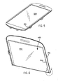
- Fig. 1 is a perspective view of an electronic mobile device according to the present disclosure
- Fig. 2 is a perspective section view of a display assembly and a gasket of the electronic mobile device along line 2-2 of Fig. 1 ;
- Fig. 3 is a front section view of the display assembly and the gasket along line 2-2 of Fig. 1 ;
- Fig. 4 is a flow chart illustrating a manufacturing process for the electronic mobile device of Fig. 1 ;
- Fig. 5 is a perspective view of a manufacturing subassembly including a spacer of the display assembly connected to a display base;
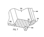
- Fig. 6 is a perspective section view of a manufacturing subassembly including the gasket connected to the spacer of Fig. 5 ;
- Fig. 7 is a detail perspective view of the subassembly of Fig. 6 enclosed by line 7-7;
- Fig. 8 is an exploded perspective view of a manufacturing subassembly including the subassembly of Fig. 6 , adhesives, a display, and an outer panel;
- Fig. 9 is a detail section view of the subassembly of Fig. 8 ;
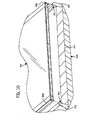
- Fig. 10 is an exploded section view of a manufacturing subassembly including the subassembly of Fig. 8 and a device housing;
- Fig. 11 is a section view illustrating deformation of the gasket due to engagement with the device housing.
- an electronic mobile device comprises a device housing and a spacer supported within the device housing.
- An outer panel is supported by the spacer, and the outer panel and the spacer together define an internal recess.
- a display configured to display information is supported by the device housing within the internal recess.
- a gasket is compressed between the device housing, the spacer, and the outer panel to inhibit debris ingress to the device housing. The gasket has a first side that engages the device housing and a second side that engages the spacer and the outer panel.
- the teachings of the present disclosure relate generally to portable electronic devices, e.g., mobile communication devices such as pagers, cellular phones, global positioning system (GPS) navigation devices and other satellite navigation devices, smart phones, wireless organizers, wireless personal digital assistants (PDA), and tablet computers.
- the portable electronic devices could be devices without wireless communication capabilities such as PDAs, electronic gaming devices, digital photograph albums or picture frames, digital cameras, or digital video recorders. These examples are intended to be non-limiting. It is also possible that the teachings of the present disclosure could be applied to electronic devices other than handheld electronic devices, e.g., notebook computers.
- an electronic mobile device 100 includes a device housing 102 that supports electronic components 204 ( Fig. 2 ) and a display assembly 106.
- a seal or gasket 208 is supported between the device housing 102 and the display assembly 106 to prevent debris ingress to the device housing 102.
- the gasket 208 also transfers impact forces to more rugged components of the display assembly 106 and away from delicate components.
- the structure of the gasket 208, the display assembly 108, and the device housing 102 facilitate ease of manufacturing and assembly.
- the device housing 102 is a generally open-top box shaped component. That is, the device housing 102 includes a back wall 210 ( Fig. 2 ) and a plurality of side walls 112 extending away from the edges of the back wall 210. Together, the back wall 210 and the side walls 112 define a front recess 214 ( Fig. 2 ) in which other components of the device 100 are housed.
- the side walls 112 also define a gasket channel 319 ( Fig. 3 ) that extends along the inner perimeter of the side walls 112. That is, the gasket channel 319 faces the front recess 214 of the device housing 102.
- the back wall 210 and the side walls 112 may also support other components of the device 100, such as buttons 118, power/data ports 118, covers overlaying battery and removable memory compartments (not shown), and the like.
- the device housing 102 may comprise various materials, such as metals, polymers, combinations thereof, and the like.
- the front recess 214 of the device housing 102 houses the electronic components 204.
- these components include a microprocessor (not shown), communication modules (not shown), and signal transmitters and receivers (not shown).
- the device housing 102 may also house additional or other electronic components commonly associated with electronic mobile devices 100.
- the display assembly 106 is housed in the front recess 214 of the device housing 102 and overlays the electronic components 204.
- the display assembly 106 includes several components, some of which are used to display information and others of which are used to connect and/or protect the components that display information.
- the display assembly 106 includes a display base 220.
- the display base 220 is a generally thin and flat support component that may comprise, for example, metals, polymers, and combinations thereof.
- the display base 220 includes a plurality of holes, one of which is shown and identified by reference number 222. Each of the holes 222 receives a mounting boss 224 of a spacer 226 that extends proximate the edges of the display base 220.
- the spacer 226 generally has a rectangular cross-sectional shape and has an outer perimeter 328 ( Fig. 3 ) disposed proximate each of the side walls 112 of the device housing 102.
- the spacer 226 may comprise one or more polymers.
- the spacer 226 extends about a first adhesive 230 that overlays the display base 220.
- the first adhesive 230 may be a double-sided adhesive film that adheres to both the display base 220 and a display 232 disposed there above.
- the display 232 is a liquid crystal display (LCD), an organic light emitting diode (OLED) display, or the like.
- the display 232 has an upper or viewing surface 334 ( Fig. 3 ) on which or through which information, e.g., telephone call information, electronic address book entries, electronic calendar entries, internet web pages, SMS messages, e-mail messages, navigation directions, electronic planner entries, digital photographs, digital videos, and the like, is viewable.
- the display 232 is positioned such that the spacer 226 extends thereabout. However, an outer perimeter 236 of the display 232 is spaced apart from the spacer 226 to define a gap 338 ( Fig. 3 ) there between. As described in further detail below, the gap 338 prevents the spacer 226 from transmitting forces directly to the display 232, thereby inhibiting damaging the display 232 by, e.g., dropping the device 100.
- a second adhesive 240 overlays both the viewing surface 334 of the display 232 and the spacer 226.
- the second adhesive 240 may be transparent to permit viewing of the display 232 there through.
- the second adhesive 240 may be a double-sided adhesive film that adheres to both the display 232 and an outer panel 242 disposed there above.
- the outer panel 242 is generally thin and flat, and in some embodiments, is a transparent component comprising one or more polymers or the like.
- the outer panel 242 is a touch-sensitive panel that operates in connection with, e.g., piezoelectric sensors (not shown), capacitive sensors (not shown), or the like in order to act as an input panel for the electronic mobile device 100.
- an outer perimeter 344 ( Fig. 3 ) of the outer panel 242 is disposed proximate the side walls 112 of the device housing 102.
- the gasket 208 is disposed in the gasket channel 319 of the side walls 112 and extends about the outer perimeters of both the spacer 226 and the outer panel 242.
- the gasket 208 may have a generally rectangular cross-sectional shape with two arcuate corners and may comprise an elastically deformable polymer that is softer than the side walls 112, the spacer 226, and the outer panel 242. This permits the gasket 208 to be compressed between these components.
- a first side 348 ( Fig. 3 ) of the gasket 208 engages the side walls 112 within the gasket channel 319
- a second side 350 of the gasket 208 engages the outer perimeters of both the spacer 226 and the outer panel 242.
- the manner in which the gasket 208 is connected to the spacer 226 provides a tight fit between the gasket 208 and the display assembly 106.
- This fit in addition to the gasket 208 engaging the side walls 112, provides a seal between the display assembly 106 and the side walls 112.
- the gasket 208 prevents debris ingress to the device housing 102 between the side walls 112 and the display assembly 106.
- the spacer 226 may engage at least two thirds of the surface area of the second side 350 of the gasket 208 such that the stress caused by the contact forces is relatively low.
- the outer panel 242 may engage at most one-third of the surface area of the second side 350.
- a method for manufacturing the electronic mobile device 100 is preferably as follows.
- the spacer 226 is molded to the display base 220 ( e.g., in an insert molding operation).
- the tapered mounting bosses 224 of the spacer 226 extend through the holes 222 in the display base 220 to secure the spacer 226 to the display base 220.
- step 462 and as shown in Figs.
- the gasket 208 is molded to the spacer 226 (e.g., in a co-molding operation) opposite an internal recess 652 defined by the spacer 226 and the display base 220. That is, the gasket 208 is molded along the outer perimeter 328 of the spacer 226.
- the gasket 208 is originally formed with a cross-sectional shape 208' ( Fig. 11 ) that differs from that of the completed assembly. Specifically, the area of the second side 350 of the gasket 208 that ultimately contacts the outer panel 242 is originally offset away from the spacer 226 compared to the area of the second side 350 that contacts the spacer 226. Similarly, the area of the first side 348 opposite the offset area of the second side 350 is also offset away from the spacer 226 by a similar distance.
- the offset may be at least one-sixth of the original width (i.e ., the distance between the first side 348 and the second side 350) of the gasket 208 (e.g., about 0.1 to 0.2 mm) to permit the outer panel 242 to be easily placed within the gasket 208 as described in further detail below.
- the first adhesive 230 is connected to the display base 220 within the internal recess 652.
- This step may include, e.g., removing a liner (not shown) from the lower surface of the first adhesive 230, pressing the first adhesive 230 against the display base 220, and then removing another liner (not shown) from the upper surface of the first adhesive 230.
- the display 232 is then connected to the first adhesive 230 within the internal recess 652.
- the second adhesive 240 is overlaid and connects to both the display 232 and the spacer 226.
- This step may include, e.g., removing a liner (not shown) from the lower surface of the second adhesive 240, pressing the second adhesive 240 against the display 232 and the spacer 226, and then removing another liner (not shown) from the upper surface of the second adhesive 240.
- the outer panel 242 is then connected to the second adhesive 240.
- the second side 350 of the gasket 208 is offset from the outer panel 242 and, as such, the outer panel 242 is easily connected to the second adhesive 240 without displacing or deforming the gasket 208.
- the display assembly 106 and the gasket 208 are positioned in the device housing 102 such that the gasket 208 is received in the gasket channel 319 of the side walls 112.
- the cross-sectional area of the gasket channel 319 is less than and differs from the shape of the original cross-sectional area 208' of the gasket. As such, positioning the display assembly 106 and the gasket 208 in the device housing 102 causes the softer gasket 208 to deform and move toward the outer panel 242. The second side 350 of the gasket 208 thereby contacts the outer panel 242 to inhibit debris passage adjacent the outer panel 242.
- the electronic mobile device 100 and its method of manufacturing described above may be modified in various manners without departing from the scope of the disclosure.
- the specific cross-sectional shape of the gasket 208 may differ from that shown in the figures to provide a more circular gasket shape.
- the cross-sectional shape of the gasket 208 shown in the figures i.e., rectangular with two arcuate corners
- the present disclosure provides an electronic mobile device 100 in which a gasket 208 engages an outer display panel 242 to inhibit debris ingress and accumulation beneath the outer panel 242. Moreover, the contact force between the gasket 208 and the outer panel 242 is relatively small compared to that between the gasket 208 and a spacer 226, and therefore the majority of an impact force is transferred to the spacer 226 instead of the outer panel 242. Further still, the present disclosure provides a method for manufacturing the electronic mobile device 100 in a manner that is unlikely to damage components of the display assembly 106.
Abstract
Description
- The present disclosure generally relates to an electronic mobile device having a gasket for inhibiting debris ingress to a device housing.
- Electronic mobile devices (e.g., cellular phones, pagers, global positioning system (GPS) navigation devices and other satellite navigation devices, smart phones, wireless organizers, wireless personal digital assistants (PDAs), and the like) typically comprise delicate components (e.g., displays, electronic circuits, and the like) that can easily be damaged during everyday use. For example, an electronic mobile device display can be damaged by impact forces transferred through the outer device housing when dropped. As another example, electronic circuits within the device can be rendered inoperable if debris (e.g., dust particles) enters the device through gaps between adjacent components.
- For the above reasons, electronic mobile devices typically include one or more gaskets or seals between some adjacent components, such as the device housing and the display assembly. That is, these gaskets transfer impact forces to more rugged components (e.g., support frames within the device) and away from delicate components (e.g., display panels). In addition, the same or additional gaskets inhibit debris ingress that could damage electronic circuits
- Unfortunately, these gaskets, due to their tight positioning between adjacent components, typically make device assembly relatively difficult. For example, it can be difficult to press a display panel into a gasket that extends around the perimeter of the display panel because of the small clearances between the two components. If care is not taken during this step, the display panel could flatten part of the gasket instead of properly connecting to it, thereby partially rendering the gasket ineffective for inhibiting debris ingress. As another example, other methods for connecting a gasket to a display panel, such as co-molding, typically fail because of different material properties of the two components. In particular, display panels typically cannot tolerate the high temperatures used in co-molding operations. For these reasons, electronic mobile devices typically do not include a gasket that contacts a display panel, and debris may thereby enter and accumulate beneath the display panel.
-
Fig. 1 is a perspective view of an electronic mobile device according to the present disclosure; -
Fig. 2 is a perspective section view of a display assembly and a gasket of the electronic mobile device along line 2-2 ofFig. 1 ; -
Fig. 3 is a front section view of the display assembly and the gasket along line 2-2 ofFig. 1 ; -
Fig. 4 is a flow chart illustrating a manufacturing process for the electronic mobile device ofFig. 1 ; -
Fig. 5 is a perspective view of a manufacturing subassembly including a spacer of the display assembly connected to a display base; -
Fig. 6 is a perspective section view of a manufacturing subassembly including the gasket connected to the spacer ofFig. 5 ; -
Fig. 7 is a detail perspective view of the subassembly ofFig. 6 enclosed by line 7-7; -
Fig. 8 is an exploded perspective view of a manufacturing subassembly including the subassembly ofFig. 6 , adhesives, a display, and an outer panel; -
Fig. 9 is a detail section view of the subassembly ofFig. 8 ; -
Fig. 10 is an exploded section view of a manufacturing subassembly including the subassembly ofFig. 8 and a device housing; and -
Fig. 11 is a section view illustrating deformation of the gasket due to engagement with the device housing. - According to some embodiments, an electronic mobile device comprises a device housing and a spacer supported within the device housing. An outer panel is supported by the spacer, and the outer panel and the spacer together define an internal recess. A display configured to display information is supported by the device housing within the internal recess. A gasket is compressed between the device housing, the spacer, and the outer panel to inhibit debris ingress to the device housing. The gasket has a first side that engages the device housing and a second side that engages the spacer and the outer panel.
- The teachings of the present disclosure relate generally to portable electronic devices, e.g., mobile communication devices such as pagers, cellular phones, global positioning system (GPS) navigation devices and other satellite navigation devices, smart phones, wireless organizers, wireless personal digital assistants (PDA), and tablet computers. The portable electronic devices could be devices without wireless communication capabilities such as PDAs, electronic gaming devices, digital photograph albums or picture frames, digital cameras, or digital video recorders. These examples are intended to be non-limiting. It is also possible that the teachings of the present disclosure could be applied to electronic devices other than handheld electronic devices, e.g., notebook computers.
- Referring now to
Figs. 1-3 , an electronicmobile device 100 according to the present disclosure includes adevice housing 102 that supports electronic components 204 (Fig. 2 ) and adisplay assembly 106. A seal orgasket 208 is supported between thedevice housing 102 and thedisplay assembly 106 to prevent debris ingress to thedevice housing 102. Thegasket 208 also transfers impact forces to more rugged components of thedisplay assembly 106 and away from delicate components. Furthermore, the structure of thegasket 208, the display assembly 108, and thedevice housing 102 facilitate ease of manufacturing and assembly. These aspects and components are described in further detail in the following paragraphs, beginning with thedevice housing 102 and concluding with the manufacturing process. - Still referring to
Figs. 1-3 , thedevice housing 102 is a generally open-top box shaped component. That is, thedevice housing 102 includes a back wall 210 (Fig. 2 ) and a plurality ofside walls 112 extending away from the edges of theback wall 210. Together, theback wall 210 and theside walls 112 define a front recess 214 (Fig. 2 ) in which other components of thedevice 100 are housed. Theside walls 112 also define a gasket channel 319 (Fig. 3 ) that extends along the inner perimeter of theside walls 112. That is, thegasket channel 319 faces thefront recess 214 of thedevice housing 102. - The
back wall 210 and theside walls 112 may also support other components of thedevice 100, such asbuttons 118, power/data ports 118, covers overlaying battery and removable memory compartments (not shown), and the like. In addition, thedevice housing 102 may comprise various materials, such as metals, polymers, combinations thereof, and the like. - As described briefly above, the front recess 214 of the
device housing 102 houses theelectronic components 204. In some embodiments, these components include a microprocessor (not shown), communication modules (not shown), and signal transmitters and receivers (not shown). Thedevice housing 102 may also house additional or other electronic components commonly associated with electronicmobile devices 100. - Referring now to
Figs. 2 and3 , thedisplay assembly 106 is housed in thefront recess 214 of thedevice housing 102 and overlays theelectronic components 204. In general, thedisplay assembly 106 includes several components, some of which are used to display information and others of which are used to connect and/or protect the components that display information. Immediately above theelectronic components 204, thedisplay assembly 106 includes adisplay base 220. Thedisplay base 220 is a generally thin and flat support component that may comprise, for example, metals, polymers, and combinations thereof. Thedisplay base 220 includes a plurality of holes, one of which is shown and identified byreference number 222. Each of theholes 222 receives amounting boss 224 of aspacer 226 that extends proximate the edges of thedisplay base 220. - The
spacer 226 generally has a rectangular cross-sectional shape and has an outer perimeter 328 (Fig. 3 ) disposed proximate each of theside walls 112 of thedevice housing 102. In addition, thespacer 226 may comprise one or more polymers. Thespacer 226 extends about afirst adhesive 230 that overlays thedisplay base 220. The first adhesive 230 may be a double-sided adhesive film that adheres to both thedisplay base 220 and adisplay 232 disposed there above. - The
display 232 is a liquid crystal display (LCD), an organic light emitting diode (OLED) display, or the like. In any case, thedisplay 232 has an upper or viewing surface 334 (Fig. 3 ) on which or through which information, e.g., telephone call information, electronic address book entries, electronic calendar entries, internet web pages, SMS messages, e-mail messages, navigation directions, electronic planner entries, digital photographs, digital videos, and the like, is viewable. - The
display 232 is positioned such that thespacer 226 extends thereabout. However, anouter perimeter 236 of thedisplay 232 is spaced apart from thespacer 226 to define a gap 338 (Fig. 3 ) there between. As described in further detail below, thegap 338 prevents thespacer 226 from transmitting forces directly to thedisplay 232, thereby inhibiting damaging thedisplay 232 by, e.g., dropping thedevice 100. - A
second adhesive 240 overlays both theviewing surface 334 of thedisplay 232 and thespacer 226. Thesecond adhesive 240 may be transparent to permit viewing of thedisplay 232 there through. Furthermore, thesecond adhesive 240 may be a double-sided adhesive film that adheres to both thedisplay 232 and anouter panel 242 disposed there above. - The
outer panel 242 is generally thin and flat, and in some embodiments, is a transparent component comprising one or more polymers or the like. In some embodiments, theouter panel 242 is a touch-sensitive panel that operates in connection with, e.g., piezoelectric sensors (not shown), capacitive sensors (not shown), or the like in order to act as an input panel for the electronicmobile device 100. In any case, an outer perimeter 344 (Fig. 3 ) of theouter panel 242 is disposed proximate theside walls 112 of thedevice housing 102. - Still referring to
Figs. 2 and3 , thegasket 208 is disposed in thegasket channel 319 of theside walls 112 and extends about the outer perimeters of both thespacer 226 and theouter panel 242. Thegasket 208 may have a generally rectangular cross-sectional shape with two arcuate corners and may comprise an elastically deformable polymer that is softer than theside walls 112, thespacer 226, and theouter panel 242. This permits thegasket 208 to be compressed between these components. In particular, a first side 348 (Fig. 3 ) of thegasket 208 engages theside walls 112 within thegasket channel 319, and asecond side 350 of thegasket 208 engages the outer perimeters of both thespacer 226 and theouter panel 242. The manner in which thegasket 208 is connected to the spacer 226 (described in further detail below) provides a tight fit between thegasket 208 and thedisplay assembly 106. This fit, in addition to thegasket 208 engaging theside walls 112, provides a seal between thedisplay assembly 106 and theside walls 112. As such, thegasket 208 prevents debris ingress to thedevice housing 102 between theside walls 112 and thedisplay assembly 106. - Contact forces between the
gasket 208 and thespacer 226 are larger than those between thegasket 208 and theouter panel 242 due to the manner in which thedisplay assembly 106 is connected to the device housing 102 (described in further detail below). That is, thegasket 208 presses against theouter panel 242 more loosely than it does against thespacer 226. As a result, the majority of an impact force acting on the device housing 102 (e.g., caused by dropping the device) is transmitted to thespacer 226 or acts to press thegasket 208 more tightly against thespacer 226. This manner of reacting to impact forces inhibits the forces from damaging theouter panel 242. - Considering the contact forces described above, the
spacer 226 may engage at least two thirds of the surface area of thesecond side 350 of thegasket 208 such that the stress caused by the contact forces is relatively low. As a result, theouter panel 242 may engage at most one-third of the surface area of thesecond side 350. - Referring now to
Figs. 4-11 , a method for manufacturing the electronicmobile device 100, particularly assembling thedisplay assembly 106 and connecting thedevice housing 102, is preferably as follows. First, atstep 460 and as shown inFig. 5 , thespacer 226 is molded to the display base 220 (e.g., in an insert molding operation). As described above, the tapered mountingbosses 224 of thespacer 226 extend through theholes 222 in thedisplay base 220 to secure thespacer 226 to thedisplay base 220. Next, at step 462 and as shown inFigs. 6 and7 , thegasket 208 is molded to the spacer 226 (e.g., in a co-molding operation) opposite aninternal recess 652 defined by thespacer 226 and thedisplay base 220. That is, thegasket 208 is molded along theouter perimeter 328 of thespacer 226. - As shown most clearly in
Figs. 7 and11 , thegasket 208 is originally formed with a cross-sectional shape 208' (Fig. 11 ) that differs from that of the completed assembly. Specifically, the area of thesecond side 350 of thegasket 208 that ultimately contacts theouter panel 242 is originally offset away from thespacer 226 compared to the area of thesecond side 350 that contacts thespacer 226. Similarly, the area of thefirst side 348 opposite the offset area of thesecond side 350 is also offset away from thespacer 226 by a similar distance. The offset may be at least one-sixth of the original width (i.e., the distance between thefirst side 348 and the second side 350) of the gasket 208 (e.g., about 0.1 to 0.2 mm) to permit theouter panel 242 to be easily placed within thegasket 208 as described in further detail below. - Next, however, and at
step 464 and as shown inFig. 8 , thefirst adhesive 230 is connected to thedisplay base 220 within theinternal recess 652. This step may include, e.g., removing a liner (not shown) from the lower surface of thefirst adhesive 230, pressing thefirst adhesive 230 against thedisplay base 220, and then removing another liner (not shown) from the upper surface of thefirst adhesive 230. Atstep 466 and still referring toFig. 8 , thedisplay 232 is then connected to thefirst adhesive 230 within theinternal recess 652. - Next, at
step 468 and as shown inFig. 8 , thesecond adhesive 240 is overlaid and connects to both thedisplay 232 and thespacer 226. This step may include, e.g., removing a liner (not shown) from the lower surface of thesecond adhesive 240, pressing thesecond adhesive 240 against thedisplay 232 and thespacer 226, and then removing another liner (not shown) from the upper surface of thesecond adhesive 240. - At
step 470 and referring toFig. 9 , theouter panel 242 is then connected to thesecond adhesive 240. As described briefly above, thesecond side 350 of thegasket 208 is offset from theouter panel 242 and, as such, theouter panel 242 is easily connected to thesecond adhesive 240 without displacing or deforming thegasket 208. Lastly, at step 472 and referring toFig. 10 , thedisplay assembly 106 and thegasket 208 are positioned in thedevice housing 102 such that thegasket 208 is received in thegasket channel 319 of theside walls 112. - As shown in
Fig. 11 , the cross-sectional area of thegasket channel 319 is less than and differs from the shape of the original cross-sectional area 208' of the gasket. As such, positioning thedisplay assembly 106 and thegasket 208 in thedevice housing 102 causes thesofter gasket 208 to deform and move toward theouter panel 242. Thesecond side 350 of thegasket 208 thereby contacts theouter panel 242 to inhibit debris passage adjacent theouter panel 242. - The electronic
mobile device 100 and its method of manufacturing described above may be modified in various manners without departing from the scope of the disclosure. For example, the specific cross-sectional shape of thegasket 208 may differ from that shown in the figures to provide a more circular gasket shape. However, the cross-sectional shape of thegasket 208 shown in the figures (i.e., rectangular with two arcuate corners) allows the arcuate corners of thefirst side 348 to be slid over theside walls 112 to position thegasket 208 in thegasket channel 319, and the generally flatsecond side 350 securely engages thespacer 226 and theouter panel 242. - From the above description it, should be apparent that the present disclosure provides an electronic
mobile device 100 in which agasket 208 engages anouter display panel 242 to inhibit debris ingress and accumulation beneath theouter panel 242. Moreover, the contact force between thegasket 208 and theouter panel 242 is relatively small compared to that between thegasket 208 and aspacer 226, and therefore the majority of an impact force is transferred to thespacer 226 instead of theouter panel 242. Further still, the present disclosure provides a method for manufacturing the electronicmobile device 100 in a manner that is unlikely to damage components of thedisplay assembly 106. - The various embodiments presented above are merely examples and are in no way meant to limit the scope of this disclosure. Variations of the embodiments described herein will be apparent to persons of ordinary skill in the art, such variations being within the intended scope of the present application. In particular, features from one or more of the above-described embodiments may be selected to create alternative embodiments comprised of a sub-combination of features which may not be explicitly described above. In addition, features from one or more of the above-described embodiments may be selected and combined to create alternative embodiments comprised of a combination of features which may not be explicitly described above. Features suitable for such combinations and subcombinations would be readily apparent to persons skilled in the art upon review of the present application as a whole. The subject matter described herein and in the recited claims intends to cover and embrace all suitable changes in technology.
Claims (14)
- An electronic mobile device, comprising:a device housing (102);a spacer (226) supported within the device housing (102);an outer panel (242) supported by the spacer (226), the outer panel (242) and the spacer (226) together defining an internal recess;a display (232) configured to display information and being supported by the device housing (102) within the internal recess; anda gasket (208) compressed between the device housing (102), the spacer (226), and the outer panel (242) to inhibit debris ingress to the device housing (102), the gasket (208) having a first side (348) engaging the device housing (102) and a second side (350) engaging the spacer (226) and the outer panel (242).
- The electronic mobile device of claim 1, wherein the spacer (226) and the display (232) define a gap (338) there between to inhibit forces from being transferred from the spacer (226) directly to the display (232).
- The electronic mobile device of claim 1, wherein the second side (350) has a surface area, and the spacer (226) engages at least two-thirds of the surface area and the outer panel (242) engages at most one-third of the surface area.
- The electronic mobile device of claim 1, wherein the gasket (208) has a rectangular cross-sectional shape with two arcuate corners.
- The electronic mobile device of claim 4, wherein the two arcuate corners engage the device housing (102).
- The electronic mobile device of claim 1, wherein the gasket (208) comprises an elastically-deformable polymer.
- A method of manufacturing an electronic mobile device, comprising the steps of:providing a display base (220);connecting a spacer (226) to the display base (220) such that the spacer (226) and the display base (220) together define an internal recess;positioning a gasket (208) about an outer perimeter (328) of the spacer (226) opposite the internal recess;positioning a display (232) within the internal recess;positioning an outer panel (242) proximate the display (232) and the spacer (226) and outside of the internal recess such that an outer perimeter (344) of the outer panel (242) is spaced apart from the gasket (208); anddeforming the gasket (208) such that the gasket (208) engages the outer perimeter (344) of the outer panel (242).
- The method of claim 7, wherein the step of deforming the gasket (208) such that the gasket (208) engages the outer perimeter (344) of the outer panel (242) includes engaging a side (348) of the gasket (208) opposite the outer panel (242) with a plurality of side walls (112) of a device housing (102).
- The method of claim 8, wherein the step of engaging the gasket (208) with the plurality of side walls (112) of the device housing (102) includes positioning the gasket (208) within a gasket channel (319) defined by the plurality of side walls (112).
- The method of claim 7, wherein the step of positioning the display (232) within the internal recess includes positioning the display (232) such that an outer perimeter (236) of the display (232) is spaced apart from the spacer (226).
- The method of claim 7, wherein the step of connecting the gasket (208) about the outer perimeter (328) of the spacer (226) includes co-molding the gasket (208) to the spacer (226).
- The method of claim 7, wherein the step of connecting the spacer (226) to the display base (220) includes insert molding the spacer (226) to the display base (220).
- The method of claim 7, further comprising the step of connecting a first adhesive to the display base (220) within the internal recess, and wherein the step of positioning the display (232) within the internal recess includes connecting the display (232) to the first adhesive (230) opposite the display base (220).
- The method of claim 13, further comprising the step of connecting a second adhesive (240) to the display (232) opposite the display base (220), and wherein the step of positioning the outer panel (242) proximate the display (232) includes connecting the outer panel (242) to the second adhesive (240) opposite the display (232).
Priority Applications (2)
| Application Number | Priority Date | Filing Date | Title |
|---|---|---|---|
| EP20100179225 EP2434367B1 (en) | 2010-09-24 | 2010-09-24 | Gasket and display assembly for an electronic mobile device |
| CA 2753507 CA2753507A1 (en) | 2010-09-24 | 2011-09-23 | Gasket and display assembly for an electronic mobile device |
Applications Claiming Priority (1)
| Application Number | Priority Date | Filing Date | Title |
|---|---|---|---|
| EP20100179225 EP2434367B1 (en) | 2010-09-24 | 2010-09-24 | Gasket and display assembly for an electronic mobile device |
Publications (2)
| Publication Number | Publication Date |
|---|---|
| EP2434367A1 true EP2434367A1 (en) | 2012-03-28 |
| EP2434367B1 EP2434367B1 (en) | 2015-05-06 |
Family
ID=43532821
Family Applications (1)
| Application Number | Title | Priority Date | Filing Date |
|---|---|---|---|
| EP20100179225 Active EP2434367B1 (en) | 2010-09-24 | 2010-09-24 | Gasket and display assembly for an electronic mobile device |
Country Status (2)
| Country | Link |
|---|---|
| EP (1) | EP2434367B1 (en) |
| CA (1) | CA2753507A1 (en) |
Cited By (1)
| Publication number | Priority date | Publication date | Assignee | Title |
|---|---|---|---|---|
| WO2014102470A1 (en) * | 2012-12-27 | 2014-07-03 | Valeo Systemes Thermiques | Display module and display device comprising such a module |
Citations (3)
| Publication number | Priority date | Publication date | Assignee | Title |
|---|---|---|---|---|
| US20030048597A1 (en) * | 2001-09-07 | 2003-03-13 | Shih-Chieh Wang | Personal digital assistant with waterproof and dustproof functions |
| WO2009126480A2 (en) * | 2008-04-11 | 2009-10-15 | Apple Inc. | Portable electronic device with two-piece housing |
| US20100061055A1 (en) * | 2008-09-05 | 2010-03-11 | Apple Inc. | Handheld computing device |
-
2010
- 2010-09-24 EP EP20100179225 patent/EP2434367B1/en active Active
-
2011
- 2011-09-23 CA CA 2753507 patent/CA2753507A1/en not_active Abandoned
Patent Citations (3)
| Publication number | Priority date | Publication date | Assignee | Title |
|---|---|---|---|---|
| US20030048597A1 (en) * | 2001-09-07 | 2003-03-13 | Shih-Chieh Wang | Personal digital assistant with waterproof and dustproof functions |
| WO2009126480A2 (en) * | 2008-04-11 | 2009-10-15 | Apple Inc. | Portable electronic device with two-piece housing |
| US20100061055A1 (en) * | 2008-09-05 | 2010-03-11 | Apple Inc. | Handheld computing device |
Cited By (3)
| Publication number | Priority date | Publication date | Assignee | Title |
|---|---|---|---|---|
| WO2014102470A1 (en) * | 2012-12-27 | 2014-07-03 | Valeo Systemes Thermiques | Display module and display device comprising such a module |
| FR3000590A1 (en) * | 2012-12-27 | 2014-07-04 | Valeo Systemes Thermiques | DISPLAY MODULE AND DISPLAY DEVICE HAVING SUCH A MODULE |
| CN105378580A (en) * | 2012-12-27 | 2016-03-02 | 法雷奥热系统公司 | Display module and display device comprising such a module |
Also Published As
| Publication number | Publication date |
|---|---|
| CA2753507A1 (en) | 2012-03-24 |
| EP2434367B1 (en) | 2015-05-06 |
Similar Documents
| Publication | Publication Date | Title |
|---|---|---|
| US8508927B2 (en) | Gasket and display assembly for an electronic mobile device | |
| US8060168B2 (en) | Dust sealing tape and display using same and method of sealing | |
| US9575522B2 (en) | Mobile terminal and manufacturing method for heat spreader module | |
| CN204967873U (en) | Mobile terminal with front camera and large LCD | |
| EP1675363B1 (en) | Dustproof structure and dust entry preventing method and electronic device having same dustproof structure | |
| US9232667B2 (en) | Display device | |
| CN202217735U (en) | Battery assembly and small shape factor calculating device | |
| CN107835281B (en) | Terminal | |
| JP5684914B2 (en) | Mobile terminal | |
| KR20120041609A (en) | Button switch assembly of mobile terminal | |
| US8541697B2 (en) | Dustproof structure and electronic device employing the same | |
| US20090262424A1 (en) | Display screen assembly | |
| US20090305580A1 (en) | Mobile terminal | |
| US20120229390A1 (en) | Mobile device | |
| KR20120041605A (en) | Connector cover assembly of mobile terminal | |
| EP2434367A1 (en) | Gasket and display assembly for an electronic mobile device | |
| CN110447002B (en) | Terminal | |
| CN210225469U (en) | Mobile terminal and middle frame | |
| KR101604488B1 (en) | Backlight unit and liquid crystal display device having the same | |
| EP3053275B1 (en) | Mobile terminal | |
| CN209787211U (en) | Terminal device | |
| JP2010197925A (en) | Electro-optical device and electronic apparatus | |
| US20100328869A1 (en) | Portable electronic device | |
| CN216565725U (en) | Flexible circuit board, display module assembly and electronic equipment | |
| CN111708197B (en) | Display device and manufacturing method thereof |
Legal Events
| Date | Code | Title | Description |
|---|---|---|---|
| PUAI | Public reference made under article 153(3) epc to a published international application that has entered the european phase |
Free format text: ORIGINAL CODE: 0009012 |
|
| 17P | Request for examination filed |
Effective date: 20100924 |
|
| AK | Designated contracting states |
Kind code of ref document: A1 Designated state(s): AL AT BE BG CH CY CZ DE DK EE ES FI FR GB GR HR HU IE IS IT LI LT LU LV MC MK MT NL NO PL PT RO SE SI SK SM TR |
|
| AX | Request for extension of the european patent |
Extension state: BA ME RS |
|
| 17Q | First examination report despatched |
Effective date: 20130626 |
|
| RAP1 | Party data changed (applicant data changed or rights of an application transferred) |
Owner name: BLACKBERRY LIMITED |
|
| RAP1 | Party data changed (applicant data changed or rights of an application transferred) |
Owner name: BLACKBERRY LIMITED |
|
| REG | Reference to a national code |
Ref country code: DE Ref legal event code: R079 Ref document number: 602010024434 Country of ref document: DE Free format text: PREVIOUS MAIN CLASS: G06F0001160000 Ipc: H04M0001020000 |
|
| GRAP | Despatch of communication of intention to grant a patent |
Free format text: ORIGINAL CODE: EPIDOSNIGR1 |
|
| RIC1 | Information provided on ipc code assigned before grant |
Ipc: H04M 1/18 20060101ALN20141029BHEP Ipc: H04M 1/02 20060101AFI20141029BHEP Ipc: G06F 1/16 20060101ALI20141029BHEP |
|
| INTG | Intention to grant announced |
Effective date: 20141128 |
|
| GRAS | Grant fee paid |
Free format text: ORIGINAL CODE: EPIDOSNIGR3 |
|
| GRAA | (expected) grant |
Free format text: ORIGINAL CODE: 0009210 |
|
| STAA | Information on the status of an ep patent application or granted ep patent |
Free format text: STATUS: THE PATENT HAS BEEN GRANTED |
|
| AK | Designated contracting states |
Kind code of ref document: B1 Designated state(s): AL AT BE BG CH CY CZ DE DK EE ES FI FR GB GR HR HU IE IS IT LI LT LU LV MC MK MT NL NO PL PT RO SE SI SK SM TR |
|
| REG | Reference to a national code |
Ref country code: GB Ref legal event code: FG4D |
|
| REG | Reference to a national code |
Ref country code: CH Ref legal event code: EP |
|
| REG | Reference to a national code |
Ref country code: IE Ref legal event code: FG4D |
|
| REG | Reference to a national code |
Ref country code: AT Ref legal event code: REF Ref document number: 726377 Country of ref document: AT Kind code of ref document: T Effective date: 20150615 |
|
| REG | Reference to a national code |
Ref country code: DE Ref legal event code: R096 Ref document number: 602010024434 Country of ref document: DE Effective date: 20150618 |
|
| REG | Reference to a national code |
Ref country code: AT Ref legal event code: MK05 Ref document number: 726377 Country of ref document: AT Kind code of ref document: T Effective date: 20150506 |
|
| REG | Reference to a national code |
Ref country code: NL Ref legal event code: MP Effective date: 20150506 |
|
| REG | Reference to a national code |
Ref country code: LT Ref legal event code: MG4D |
|
| PG25 | Lapsed in a contracting state [announced via postgrant information from national office to epo] |
Ref country code: FI Free format text: LAPSE BECAUSE OF FAILURE TO SUBMIT A TRANSLATION OF THE DESCRIPTION OR TO PAY THE FEE WITHIN THE PRESCRIBED TIME-LIMIT Effective date: 20150506 Ref country code: LT Free format text: LAPSE BECAUSE OF FAILURE TO SUBMIT A TRANSLATION OF THE DESCRIPTION OR TO PAY THE FEE WITHIN THE PRESCRIBED TIME-LIMIT Effective date: 20150506 Ref country code: HR Free format text: LAPSE BECAUSE OF FAILURE TO SUBMIT A TRANSLATION OF THE DESCRIPTION OR TO PAY THE FEE WITHIN THE PRESCRIBED TIME-LIMIT Effective date: 20150506 Ref country code: NO Free format text: LAPSE BECAUSE OF FAILURE TO SUBMIT A TRANSLATION OF THE DESCRIPTION OR TO PAY THE FEE WITHIN THE PRESCRIBED TIME-LIMIT Effective date: 20150806 Ref country code: PT Free format text: LAPSE BECAUSE OF FAILURE TO SUBMIT A TRANSLATION OF THE DESCRIPTION OR TO PAY THE FEE WITHIN THE PRESCRIBED TIME-LIMIT Effective date: 20150907 Ref country code: ES Free format text: LAPSE BECAUSE OF FAILURE TO SUBMIT A TRANSLATION OF THE DESCRIPTION OR TO PAY THE FEE WITHIN THE PRESCRIBED TIME-LIMIT Effective date: 20150506 |
|
| PG25 | Lapsed in a contracting state [announced via postgrant information from national office to epo] |
Ref country code: GR Free format text: LAPSE BECAUSE OF FAILURE TO SUBMIT A TRANSLATION OF THE DESCRIPTION OR TO PAY THE FEE WITHIN THE PRESCRIBED TIME-LIMIT Effective date: 20150807 Ref country code: BG Free format text: LAPSE BECAUSE OF FAILURE TO SUBMIT A TRANSLATION OF THE DESCRIPTION OR TO PAY THE FEE WITHIN THE PRESCRIBED TIME-LIMIT Effective date: 20150806 Ref country code: IS Free format text: LAPSE BECAUSE OF FAILURE TO SUBMIT A TRANSLATION OF THE DESCRIPTION OR TO PAY THE FEE WITHIN THE PRESCRIBED TIME-LIMIT Effective date: 20150906 Ref country code: LV Free format text: LAPSE BECAUSE OF FAILURE TO SUBMIT A TRANSLATION OF THE DESCRIPTION OR TO PAY THE FEE WITHIN THE PRESCRIBED TIME-LIMIT Effective date: 20150506 Ref country code: AT Free format text: LAPSE BECAUSE OF FAILURE TO SUBMIT A TRANSLATION OF THE DESCRIPTION OR TO PAY THE FEE WITHIN THE PRESCRIBED TIME-LIMIT Effective date: 20150506 |
|
| PG25 | Lapsed in a contracting state [announced via postgrant information from national office to epo] |
Ref country code: DK Free format text: LAPSE BECAUSE OF FAILURE TO SUBMIT A TRANSLATION OF THE DESCRIPTION OR TO PAY THE FEE WITHIN THE PRESCRIBED TIME-LIMIT Effective date: 20150506 Ref country code: EE Free format text: LAPSE BECAUSE OF FAILURE TO SUBMIT A TRANSLATION OF THE DESCRIPTION OR TO PAY THE FEE WITHIN THE PRESCRIBED TIME-LIMIT Effective date: 20150506 |
|
| REG | Reference to a national code |
Ref country code: DE Ref legal event code: R097 Ref document number: 602010024434 Country of ref document: DE |
|
| PG25 | Lapsed in a contracting state [announced via postgrant information from national office to epo] |
Ref country code: RO Free format text: LAPSE BECAUSE OF NON-PAYMENT OF DUE FEES Effective date: 20150506 Ref country code: CZ Free format text: LAPSE BECAUSE OF FAILURE TO SUBMIT A TRANSLATION OF THE DESCRIPTION OR TO PAY THE FEE WITHIN THE PRESCRIBED TIME-LIMIT Effective date: 20150506 Ref country code: PL Free format text: LAPSE BECAUSE OF FAILURE TO SUBMIT A TRANSLATION OF THE DESCRIPTION OR TO PAY THE FEE WITHIN THE PRESCRIBED TIME-LIMIT Effective date: 20150506 Ref country code: SK Free format text: LAPSE BECAUSE OF FAILURE TO SUBMIT A TRANSLATION OF THE DESCRIPTION OR TO PAY THE FEE WITHIN THE PRESCRIBED TIME-LIMIT Effective date: 20150506 |
|
| PLBE | No opposition filed within time limit |
Free format text: ORIGINAL CODE: 0009261 |
|
| STAA | Information on the status of an ep patent application or granted ep patent |
Free format text: STATUS: NO OPPOSITION FILED WITHIN TIME LIMIT |
|
| 26N | No opposition filed |
Effective date: 20160209 |
|
| PG25 | Lapsed in a contracting state [announced via postgrant information from national office to epo] |
Ref country code: MC Free format text: LAPSE BECAUSE OF FAILURE TO SUBMIT A TRANSLATION OF THE DESCRIPTION OR TO PAY THE FEE WITHIN THE PRESCRIBED TIME-LIMIT Effective date: 20150506 Ref country code: LU Free format text: LAPSE BECAUSE OF FAILURE TO SUBMIT A TRANSLATION OF THE DESCRIPTION OR TO PAY THE FEE WITHIN THE PRESCRIBED TIME-LIMIT Effective date: 20150924 Ref country code: IT Free format text: LAPSE BECAUSE OF FAILURE TO SUBMIT A TRANSLATION OF THE DESCRIPTION OR TO PAY THE FEE WITHIN THE PRESCRIBED TIME-LIMIT Effective date: 20150506 |
|
| REG | Reference to a national code |
Ref country code: CH Ref legal event code: PL |
|
| PG25 | Lapsed in a contracting state [announced via postgrant information from national office to epo] |
Ref country code: SI Free format text: LAPSE BECAUSE OF FAILURE TO SUBMIT A TRANSLATION OF THE DESCRIPTION OR TO PAY THE FEE WITHIN THE PRESCRIBED TIME-LIMIT Effective date: 20150506 |
|
| REG | Reference to a national code |
Ref country code: IE Ref legal event code: MM4A |
|
| PG25 | Lapsed in a contracting state [announced via postgrant information from national office to epo] |
Ref country code: LI Free format text: LAPSE BECAUSE OF NON-PAYMENT OF DUE FEES Effective date: 20150930 Ref country code: CH Free format text: LAPSE BECAUSE OF NON-PAYMENT OF DUE FEES Effective date: 20150930 Ref country code: IE Free format text: LAPSE BECAUSE OF NON-PAYMENT OF DUE FEES Effective date: 20150924 |
|
| PG25 | Lapsed in a contracting state [announced via postgrant information from national office to epo] |
Ref country code: BE Free format text: LAPSE BECAUSE OF FAILURE TO SUBMIT A TRANSLATION OF THE DESCRIPTION OR TO PAY THE FEE WITHIN THE PRESCRIBED TIME-LIMIT Effective date: 20150506 |
|
| REG | Reference to a national code |
Ref country code: FR Ref legal event code: PLFP Year of fee payment: 7 |
|
| PG25 | Lapsed in a contracting state [announced via postgrant information from national office to epo] |
Ref country code: MT Free format text: LAPSE BECAUSE OF FAILURE TO SUBMIT A TRANSLATION OF THE DESCRIPTION OR TO PAY THE FEE WITHIN THE PRESCRIBED TIME-LIMIT Effective date: 20150506 |
|
| PG25 | Lapsed in a contracting state [announced via postgrant information from national office to epo] |
Ref country code: HU Free format text: LAPSE BECAUSE OF FAILURE TO SUBMIT A TRANSLATION OF THE DESCRIPTION OR TO PAY THE FEE WITHIN THE PRESCRIBED TIME-LIMIT; INVALID AB INITIO Effective date: 20100924 Ref country code: SM Free format text: LAPSE BECAUSE OF FAILURE TO SUBMIT A TRANSLATION OF THE DESCRIPTION OR TO PAY THE FEE WITHIN THE PRESCRIBED TIME-LIMIT Effective date: 20150506 |
|
| PG25 | Lapsed in a contracting state [announced via postgrant information from national office to epo] |
Ref country code: CY Free format text: LAPSE BECAUSE OF FAILURE TO SUBMIT A TRANSLATION OF THE DESCRIPTION OR TO PAY THE FEE WITHIN THE PRESCRIBED TIME-LIMIT Effective date: 20150506 Ref country code: SE Free format text: LAPSE BECAUSE OF FAILURE TO SUBMIT A TRANSLATION OF THE DESCRIPTION OR TO PAY THE FEE WITHIN THE PRESCRIBED TIME-LIMIT Effective date: 20150506 Ref country code: NL Free format text: LAPSE BECAUSE OF FAILURE TO SUBMIT A TRANSLATION OF THE DESCRIPTION OR TO PAY THE FEE WITHIN THE PRESCRIBED TIME-LIMIT Effective date: 20150506 |
|
| PG25 | Lapsed in a contracting state [announced via postgrant information from national office to epo] |
Ref country code: TR Free format text: LAPSE BECAUSE OF FAILURE TO SUBMIT A TRANSLATION OF THE DESCRIPTION OR TO PAY THE FEE WITHIN THE PRESCRIBED TIME-LIMIT Effective date: 20150506 |
|
| REG | Reference to a national code |
Ref country code: FR Ref legal event code: PLFP Year of fee payment: 8 |
|
| PG25 | Lapsed in a contracting state [announced via postgrant information from national office to epo] |
Ref country code: MK Free format text: LAPSE BECAUSE OF FAILURE TO SUBMIT A TRANSLATION OF THE DESCRIPTION OR TO PAY THE FEE WITHIN THE PRESCRIBED TIME-LIMIT Effective date: 20150506 |
|
| REG | Reference to a national code |
Ref country code: FR Ref legal event code: PLFP Year of fee payment: 9 |
|
| PG25 | Lapsed in a contracting state [announced via postgrant information from national office to epo] |
Ref country code: AL Free format text: LAPSE BECAUSE OF FAILURE TO SUBMIT A TRANSLATION OF THE DESCRIPTION OR TO PAY THE FEE WITHIN THE PRESCRIBED TIME-LIMIT Effective date: 20150506 |
|
| PGFP | Annual fee paid to national office [announced via postgrant information from national office to epo] |
Ref country code: GB Payment date: 20230927 Year of fee payment: 14 |
|
| PGFP | Annual fee paid to national office [announced via postgrant information from national office to epo] |
Ref country code: FR Payment date: 20230925 Year of fee payment: 14 Ref country code: DE Payment date: 20230927 Year of fee payment: 14 |