EP2434297A1 - Structure having chip mounted thereon and module provided with the structure - Google Patents
Structure having chip mounted thereon and module provided with the structure Download PDFInfo
- Publication number
- EP2434297A1 EP2434297A1 EP09844914A EP09844914A EP2434297A1 EP 2434297 A1 EP2434297 A1 EP 2434297A1 EP 09844914 A EP09844914 A EP 09844914A EP 09844914 A EP09844914 A EP 09844914A EP 2434297 A1 EP2434297 A1 EP 2434297A1
- Authority
- EP
- European Patent Office
- Prior art keywords
- adhesive agent
- chip
- substrate
- acceleration sensor
- base
- Prior art date
- Legal status (The legal status is an assumption and is not a legal conclusion. Google has not performed a legal analysis and makes no representation as to the accuracy of the status listed.)
- Ceased
Links
Images








Classifications
-
- G—PHYSICS
- G01—MEASURING; TESTING
- G01P—MEASURING LINEAR OR ANGULAR SPEED, ACCELERATION, DECELERATION, OR SHOCK; INDICATING PRESENCE, ABSENCE, OR DIRECTION, OF MOVEMENT
- G01P15/00—Measuring acceleration; Measuring deceleration; Measuring shock, i.e. sudden change of acceleration
- G01P15/02—Measuring acceleration; Measuring deceleration; Measuring shock, i.e. sudden change of acceleration by making use of inertia forces using solid seismic masses
- G01P15/08—Measuring acceleration; Measuring deceleration; Measuring shock, i.e. sudden change of acceleration by making use of inertia forces using solid seismic masses with conversion into electric or magnetic values
- G01P15/12—Measuring acceleration; Measuring deceleration; Measuring shock, i.e. sudden change of acceleration by making use of inertia forces using solid seismic masses with conversion into electric or magnetic values by alteration of electrical resistance
- G01P15/123—Measuring acceleration; Measuring deceleration; Measuring shock, i.e. sudden change of acceleration by making use of inertia forces using solid seismic masses with conversion into electric or magnetic values by alteration of electrical resistance by piezo-resistive elements, e.g. semiconductor strain gauges
-
- G—PHYSICS
- G01—MEASURING; TESTING
- G01P—MEASURING LINEAR OR ANGULAR SPEED, ACCELERATION, DECELERATION, OR SHOCK; INDICATING PRESENCE, ABSENCE, OR DIRECTION, OF MOVEMENT
- G01P15/00—Measuring acceleration; Measuring deceleration; Measuring shock, i.e. sudden change of acceleration
- G01P15/02—Measuring acceleration; Measuring deceleration; Measuring shock, i.e. sudden change of acceleration by making use of inertia forces using solid seismic masses
- G01P15/08—Measuring acceleration; Measuring deceleration; Measuring shock, i.e. sudden change of acceleration by making use of inertia forces using solid seismic masses with conversion into electric or magnetic values
-
- B—PERFORMING OPERATIONS; TRANSPORTING
- B81—MICROSTRUCTURAL TECHNOLOGY
- B81B—MICROSTRUCTURAL DEVICES OR SYSTEMS, e.g. MICROMECHANICAL DEVICES
- B81B7/00—Microstructural systems ; Auxiliary parts of microstructural devices or systems
- B81B7/0032—Packages or encapsulation
- B81B7/0045—Packages or encapsulation for reducing stress inside of the package structure
- B81B7/0048—Packages or encapsulation for reducing stress inside of the package structure between the MEMS die and the substrate
-
- G—PHYSICS
- G01—MEASURING; TESTING
- G01P—MEASURING LINEAR OR ANGULAR SPEED, ACCELERATION, DECELERATION, OR SHOCK; INDICATING PRESENCE, ABSENCE, OR DIRECTION, OF MOVEMENT
- G01P1/00—Details of instruments
- G01P1/02—Housings
- G01P1/023—Housings for acceleration measuring devices
-
- G—PHYSICS
- G01—MEASURING; TESTING
- G01P—MEASURING LINEAR OR ANGULAR SPEED, ACCELERATION, DECELERATION, OR SHOCK; INDICATING PRESENCE, ABSENCE, OR DIRECTION, OF MOVEMENT
- G01P15/00—Measuring acceleration; Measuring deceleration; Measuring shock, i.e. sudden change of acceleration
- G01P15/02—Measuring acceleration; Measuring deceleration; Measuring shock, i.e. sudden change of acceleration by making use of inertia forces using solid seismic masses
- G01P15/08—Measuring acceleration; Measuring deceleration; Measuring shock, i.e. sudden change of acceleration by making use of inertia forces using solid seismic masses with conversion into electric or magnetic values
- G01P15/0802—Details
-
- G—PHYSICS
- G01—MEASURING; TESTING
- G01P—MEASURING LINEAR OR ANGULAR SPEED, ACCELERATION, DECELERATION, OR SHOCK; INDICATING PRESENCE, ABSENCE, OR DIRECTION, OF MOVEMENT
- G01P15/00—Measuring acceleration; Measuring deceleration; Measuring shock, i.e. sudden change of acceleration
- G01P15/02—Measuring acceleration; Measuring deceleration; Measuring shock, i.e. sudden change of acceleration by making use of inertia forces using solid seismic masses
- G01P15/08—Measuring acceleration; Measuring deceleration; Measuring shock, i.e. sudden change of acceleration by making use of inertia forces using solid seismic masses with conversion into electric or magnetic values
- G01P15/12—Measuring acceleration; Measuring deceleration; Measuring shock, i.e. sudden change of acceleration by making use of inertia forces using solid seismic masses with conversion into electric or magnetic values by alteration of electrical resistance
-
- G—PHYSICS
- G01—MEASURING; TESTING
- G01P—MEASURING LINEAR OR ANGULAR SPEED, ACCELERATION, DECELERATION, OR SHOCK; INDICATING PRESENCE, ABSENCE, OR DIRECTION, OF MOVEMENT
- G01P15/00—Measuring acceleration; Measuring deceleration; Measuring shock, i.e. sudden change of acceleration
- G01P15/18—Measuring acceleration; Measuring deceleration; Measuring shock, i.e. sudden change of acceleration in two or more dimensions
-
- H—ELECTRICITY
- H10—SEMICONDUCTOR DEVICES; ELECTRIC SOLID-STATE DEVICES NOT OTHERWISE PROVIDED FOR
- H10W—GENERIC PACKAGES, INTERCONNECTIONS, CONNECTORS OR OTHER CONSTRUCTIONAL DETAILS OF DEVICES COVERED BY CLASS H10
- H10W72/00—Interconnections or connectors in packages
-
- H—ELECTRICITY
- H10—SEMICONDUCTOR DEVICES; ELECTRIC SOLID-STATE DEVICES NOT OTHERWISE PROVIDED FOR
- H10W—GENERIC PACKAGES, INTERCONNECTIONS, CONNECTORS OR OTHER CONSTRUCTIONAL DETAILS OF DEVICES COVERED BY CLASS H10
- H10W90/00—Package configurations
-
- G—PHYSICS
- G01—MEASURING; TESTING
- G01P—MEASURING LINEAR OR ANGULAR SPEED, ACCELERATION, DECELERATION, OR SHOCK; INDICATING PRESENCE, ABSENCE, OR DIRECTION, OF MOVEMENT
- G01P15/00—Measuring acceleration; Measuring deceleration; Measuring shock, i.e. sudden change of acceleration
- G01P15/02—Measuring acceleration; Measuring deceleration; Measuring shock, i.e. sudden change of acceleration by making use of inertia forces using solid seismic masses
- G01P15/08—Measuring acceleration; Measuring deceleration; Measuring shock, i.e. sudden change of acceleration by making use of inertia forces using solid seismic masses with conversion into electric or magnetic values
- G01P2015/0805—Measuring acceleration; Measuring deceleration; Measuring shock, i.e. sudden change of acceleration by making use of inertia forces using solid seismic masses with conversion into electric or magnetic values being provided with a particular type of spring-mass-system for defining the displacement of a seismic mass due to an external acceleration
- G01P2015/0822—Measuring acceleration; Measuring deceleration; Measuring shock, i.e. sudden change of acceleration by making use of inertia forces using solid seismic masses with conversion into electric or magnetic values being provided with a particular type of spring-mass-system for defining the displacement of a seismic mass due to an external acceleration for defining out-of-plane movement of the mass
- G01P2015/084—Measuring acceleration; Measuring deceleration; Measuring shock, i.e. sudden change of acceleration by making use of inertia forces using solid seismic masses with conversion into electric or magnetic values being provided with a particular type of spring-mass-system for defining the displacement of a seismic mass due to an external acceleration for defining out-of-plane movement of the mass the mass being suspended at more than one of its sides, e.g. membrane-type suspension, so as to permit multi-axis movement of the mass
- G01P2015/0842—Measuring acceleration; Measuring deceleration; Measuring shock, i.e. sudden change of acceleration by making use of inertia forces using solid seismic masses with conversion into electric or magnetic values being provided with a particular type of spring-mass-system for defining the displacement of a seismic mass due to an external acceleration for defining out-of-plane movement of the mass the mass being suspended at more than one of its sides, e.g. membrane-type suspension, so as to permit multi-axis movement of the mass the mass being of clover leaf shape
-
- H—ELECTRICITY
- H10—SEMICONDUCTOR DEVICES; ELECTRIC SOLID-STATE DEVICES NOT OTHERWISE PROVIDED FOR
- H10W—GENERIC PACKAGES, INTERCONNECTIONS, CONNECTORS OR OTHER CONSTRUCTIONAL DETAILS OF DEVICES COVERED BY CLASS H10
- H10W70/00—Package substrates; Interposers; Redistribution layers [RDL]
- H10W70/60—Insulating or insulated package substrates; Interposers; Redistribution layers
- H10W70/67—Insulating or insulated package substrates; Interposers; Redistribution layers characterised by their insulating layers or insulating parts
- H10W70/68—Shapes or dispositions thereof
- H10W70/682—Shapes or dispositions thereof comprising holes having chips therein
-
- H—ELECTRICITY
- H10—SEMICONDUCTOR DEVICES; ELECTRIC SOLID-STATE DEVICES NOT OTHERWISE PROVIDED FOR
- H10W—GENERIC PACKAGES, INTERCONNECTIONS, CONNECTORS OR OTHER CONSTRUCTIONAL DETAILS OF DEVICES COVERED BY CLASS H10
- H10W72/00—Interconnections or connectors in packages
- H10W72/071—Connecting or disconnecting
- H10W72/072—Connecting or disconnecting of bump connectors
-
- H—ELECTRICITY
- H10—SEMICONDUCTOR DEVICES; ELECTRIC SOLID-STATE DEVICES NOT OTHERWISE PROVIDED FOR
- H10W—GENERIC PACKAGES, INTERCONNECTIONS, CONNECTORS OR OTHER CONSTRUCTIONAL DETAILS OF DEVICES COVERED BY CLASS H10
- H10W72/00—Interconnections or connectors in packages
- H10W72/071—Connecting or disconnecting
- H10W72/072—Connecting or disconnecting of bump connectors
- H10W72/07231—Techniques
- H10W72/07237—Techniques using a polymer adhesive, e.g. an adhesive based on silicone or epoxy
-
- H—ELECTRICITY
- H10—SEMICONDUCTOR DEVICES; ELECTRIC SOLID-STATE DEVICES NOT OTHERWISE PROVIDED FOR
- H10W—GENERIC PACKAGES, INTERCONNECTIONS, CONNECTORS OR OTHER CONSTRUCTIONAL DETAILS OF DEVICES COVERED BY CLASS H10
- H10W72/00—Interconnections or connectors in packages
- H10W72/071—Connecting or disconnecting
- H10W72/072—Connecting or disconnecting of bump connectors
- H10W72/07251—Connecting or disconnecting of bump connectors characterised by changes in properties of the bump connectors during connecting
- H10W72/07252—Connecting or disconnecting of bump connectors characterised by changes in properties of the bump connectors during connecting changes in structures or sizes
-
- H—ELECTRICITY
- H10—SEMICONDUCTOR DEVICES; ELECTRIC SOLID-STATE DEVICES NOT OTHERWISE PROVIDED FOR
- H10W—GENERIC PACKAGES, INTERCONNECTIONS, CONNECTORS OR OTHER CONSTRUCTIONAL DETAILS OF DEVICES COVERED BY CLASS H10
- H10W72/00—Interconnections or connectors in packages
- H10W72/071—Connecting or disconnecting
- H10W72/073—Connecting or disconnecting of die-attach connectors
-
- H—ELECTRICITY
- H10—SEMICONDUCTOR DEVICES; ELECTRIC SOLID-STATE DEVICES NOT OTHERWISE PROVIDED FOR
- H10W—GENERIC PACKAGES, INTERCONNECTIONS, CONNECTORS OR OTHER CONSTRUCTIONAL DETAILS OF DEVICES COVERED BY CLASS H10
- H10W72/00—Interconnections or connectors in packages
- H10W72/071—Connecting or disconnecting
- H10W72/073—Connecting or disconnecting of die-attach connectors
- H10W72/07351—Connecting or disconnecting of die-attach connectors characterised by changes in properties of the die-attach connectors during connecting
- H10W72/07354—Connecting or disconnecting of die-attach connectors characterised by changes in properties of the die-attach connectors during connecting changes in dispositions
-
- H—ELECTRICITY
- H10—SEMICONDUCTOR DEVICES; ELECTRIC SOLID-STATE DEVICES NOT OTHERWISE PROVIDED FOR
- H10W—GENERIC PACKAGES, INTERCONNECTIONS, CONNECTORS OR OTHER CONSTRUCTIONAL DETAILS OF DEVICES COVERED BY CLASS H10
- H10W72/00—Interconnections or connectors in packages
- H10W72/20—Bump connectors, e.g. solder bumps or copper pillars; Dummy bumps; Thermal bumps
- H10W72/221—Structures or relative sizes
- H10W72/222—Multilayered bumps, e.g. a coating on top and side surfaces of a bump core
- H10W72/223—Multilayered bumps, e.g. a coating on top and side surfaces of a bump core characterised by the structure of the outermost layers, e.g. multilayered coatings
-
- H—ELECTRICITY
- H10—SEMICONDUCTOR DEVICES; ELECTRIC SOLID-STATE DEVICES NOT OTHERWISE PROVIDED FOR
- H10W—GENERIC PACKAGES, INTERCONNECTIONS, CONNECTORS OR OTHER CONSTRUCTIONAL DETAILS OF DEVICES COVERED BY CLASS H10
- H10W72/00—Interconnections or connectors in packages
- H10W72/20—Bump connectors, e.g. solder bumps or copper pillars; Dummy bumps; Thermal bumps
- H10W72/221—Structures or relative sizes
- H10W72/225—Bumps having a filler embedded in a matrix
-
- H—ELECTRICITY
- H10—SEMICONDUCTOR DEVICES; ELECTRIC SOLID-STATE DEVICES NOT OTHERWISE PROVIDED FOR
- H10W—GENERIC PACKAGES, INTERCONNECTIONS, CONNECTORS OR OTHER CONSTRUCTIONAL DETAILS OF DEVICES COVERED BY CLASS H10
- H10W72/00—Interconnections or connectors in packages
- H10W72/20—Bump connectors, e.g. solder bumps or copper pillars; Dummy bumps; Thermal bumps
- H10W72/221—Structures or relative sizes
- H10W72/227—Multiple bumps having different sizes
-
- H—ELECTRICITY
- H10—SEMICONDUCTOR DEVICES; ELECTRIC SOLID-STATE DEVICES NOT OTHERWISE PROVIDED FOR
- H10W—GENERIC PACKAGES, INTERCONNECTIONS, CONNECTORS OR OTHER CONSTRUCTIONAL DETAILS OF DEVICES COVERED BY CLASS H10
- H10W72/00—Interconnections or connectors in packages
- H10W72/20—Bump connectors, e.g. solder bumps or copper pillars; Dummy bumps; Thermal bumps
- H10W72/241—Dispositions, e.g. layouts
-
- H—ELECTRICITY
- H10—SEMICONDUCTOR DEVICES; ELECTRIC SOLID-STATE DEVICES NOT OTHERWISE PROVIDED FOR
- H10W—GENERIC PACKAGES, INTERCONNECTIONS, CONNECTORS OR OTHER CONSTRUCTIONAL DETAILS OF DEVICES COVERED BY CLASS H10
- H10W72/00—Interconnections or connectors in packages
- H10W72/20—Bump connectors, e.g. solder bumps or copper pillars; Dummy bumps; Thermal bumps
- H10W72/241—Dispositions, e.g. layouts
- H10W72/245—Dispositions, e.g. layouts of outermost layers of multilayered bumps, e.g. bump coating being only on a part of a bump core
-
- H—ELECTRICITY
- H10—SEMICONDUCTOR DEVICES; ELECTRIC SOLID-STATE DEVICES NOT OTHERWISE PROVIDED FOR
- H10W—GENERIC PACKAGES, INTERCONNECTIONS, CONNECTORS OR OTHER CONSTRUCTIONAL DETAILS OF DEVICES COVERED BY CLASS H10
- H10W72/00—Interconnections or connectors in packages
- H10W72/20—Bump connectors, e.g. solder bumps or copper pillars; Dummy bumps; Thermal bumps
- H10W72/241—Dispositions, e.g. layouts
- H10W72/247—Dispositions of multiple bumps
- H10W72/248—Top-view layouts, e.g. mirror arrays
-
- H—ELECTRICITY
- H10—SEMICONDUCTOR DEVICES; ELECTRIC SOLID-STATE DEVICES NOT OTHERWISE PROVIDED FOR
- H10W—GENERIC PACKAGES, INTERCONNECTIONS, CONNECTORS OR OTHER CONSTRUCTIONAL DETAILS OF DEVICES COVERED BY CLASS H10
- H10W72/00—Interconnections or connectors in packages
- H10W72/20—Bump connectors, e.g. solder bumps or copper pillars; Dummy bumps; Thermal bumps
- H10W72/251—Materials
- H10W72/252—Materials comprising solid metals or solid metalloids, e.g. PbSn, Ag or Cu
-
- H—ELECTRICITY
- H10—SEMICONDUCTOR DEVICES; ELECTRIC SOLID-STATE DEVICES NOT OTHERWISE PROVIDED FOR
- H10W—GENERIC PACKAGES, INTERCONNECTIONS, CONNECTORS OR OTHER CONSTRUCTIONAL DETAILS OF DEVICES COVERED BY CLASS H10
- H10W72/00—Interconnections or connectors in packages
- H10W72/20—Bump connectors, e.g. solder bumps or copper pillars; Dummy bumps; Thermal bumps
- H10W72/251—Materials
- H10W72/253—Materials not comprising solid metals or solid metalloids, e.g. polymers or ceramics
-
- H—ELECTRICITY
- H10—SEMICONDUCTOR DEVICES; ELECTRIC SOLID-STATE DEVICES NOT OTHERWISE PROVIDED FOR
- H10W—GENERIC PACKAGES, INTERCONNECTIONS, CONNECTORS OR OTHER CONSTRUCTIONAL DETAILS OF DEVICES COVERED BY CLASS H10
- H10W72/00—Interconnections or connectors in packages
- H10W72/20—Bump connectors, e.g. solder bumps or copper pillars; Dummy bumps; Thermal bumps
- H10W72/251—Materials
- H10W72/255—Materials of outermost layers of multilayered bumps, e.g. material of a coating
-
- H—ELECTRICITY
- H10—SEMICONDUCTOR DEVICES; ELECTRIC SOLID-STATE DEVICES NOT OTHERWISE PROVIDED FOR
- H10W—GENERIC PACKAGES, INTERCONNECTIONS, CONNECTORS OR OTHER CONSTRUCTIONAL DETAILS OF DEVICES COVERED BY CLASS H10
- H10W72/00—Interconnections or connectors in packages
- H10W72/20—Bump connectors, e.g. solder bumps or copper pillars; Dummy bumps; Thermal bumps
- H10W72/29—Bond pads specially adapted therefor
-
- H—ELECTRICITY
- H10—SEMICONDUCTOR DEVICES; ELECTRIC SOLID-STATE DEVICES NOT OTHERWISE PROVIDED FOR
- H10W—GENERIC PACKAGES, INTERCONNECTIONS, CONNECTORS OR OTHER CONSTRUCTIONAL DETAILS OF DEVICES COVERED BY CLASS H10
- H10W72/00—Interconnections or connectors in packages
- H10W72/30—Die-attach connectors
- H10W72/341—Dispositions of die-attach connectors, e.g. layouts
-
- H—ELECTRICITY
- H10—SEMICONDUCTOR DEVICES; ELECTRIC SOLID-STATE DEVICES NOT OTHERWISE PROVIDED FOR
- H10W—GENERIC PACKAGES, INTERCONNECTIONS, CONNECTORS OR OTHER CONSTRUCTIONAL DETAILS OF DEVICES COVERED BY CLASS H10
- H10W72/00—Interconnections or connectors in packages
- H10W72/30—Die-attach connectors
- H10W72/351—Materials of die-attach connectors
- H10W72/353—Materials of die-attach connectors not comprising solid metals or solid metalloids, e.g. ceramics
- H10W72/354—Materials of die-attach connectors not comprising solid metals or solid metalloids, e.g. ceramics comprising polymers
-
- H—ELECTRICITY
- H10—SEMICONDUCTOR DEVICES; ELECTRIC SOLID-STATE DEVICES NOT OTHERWISE PROVIDED FOR
- H10W—GENERIC PACKAGES, INTERCONNECTIONS, CONNECTORS OR OTHER CONSTRUCTIONAL DETAILS OF DEVICES COVERED BY CLASS H10
- H10W72/00—Interconnections or connectors in packages
- H10W72/50—Bond wires
- H10W72/541—Dispositions of bond wires
- H10W72/5445—Dispositions of bond wires being orthogonal to a side surface of the chip, e.g. parallel arrangements
-
- H—ELECTRICITY
- H10—SEMICONDUCTOR DEVICES; ELECTRIC SOLID-STATE DEVICES NOT OTHERWISE PROVIDED FOR
- H10W—GENERIC PACKAGES, INTERCONNECTIONS, CONNECTORS OR OTHER CONSTRUCTIONAL DETAILS OF DEVICES COVERED BY CLASS H10
- H10W72/00—Interconnections or connectors in packages
- H10W72/50—Bond wires
- H10W72/541—Dispositions of bond wires
- H10W72/5449—Dispositions of bond wires not being orthogonal to a side surface of the chip, e.g. fan-out arrangements
-
- H—ELECTRICITY
- H10—SEMICONDUCTOR DEVICES; ELECTRIC SOLID-STATE DEVICES NOT OTHERWISE PROVIDED FOR
- H10W—GENERIC PACKAGES, INTERCONNECTIONS, CONNECTORS OR OTHER CONSTRUCTIONAL DETAILS OF DEVICES COVERED BY CLASS H10
- H10W72/00—Interconnections or connectors in packages
- H10W72/50—Bond wires
- H10W72/551—Materials of bond wires
- H10W72/552—Materials of bond wires comprising metals or metalloids, e.g. silver
-
- H—ELECTRICITY
- H10—SEMICONDUCTOR DEVICES; ELECTRIC SOLID-STATE DEVICES NOT OTHERWISE PROVIDED FOR
- H10W—GENERIC PACKAGES, INTERCONNECTIONS, CONNECTORS OR OTHER CONSTRUCTIONAL DETAILS OF DEVICES COVERED BY CLASS H10
- H10W72/00—Interconnections or connectors in packages
- H10W72/50—Bond wires
- H10W72/59—Bond pads specially adapted therefor
-
- H—ELECTRICITY
- H10—SEMICONDUCTOR DEVICES; ELECTRIC SOLID-STATE DEVICES NOT OTHERWISE PROVIDED FOR
- H10W—GENERIC PACKAGES, INTERCONNECTIONS, CONNECTORS OR OTHER CONSTRUCTIONAL DETAILS OF DEVICES COVERED BY CLASS H10
- H10W72/00—Interconnections or connectors in packages
- H10W72/851—Dispositions of multiple connectors or interconnections
- H10W72/853—On the same surface
- H10W72/856—Bump connectors and die-attach connectors
-
- H—ELECTRICITY
- H10—SEMICONDUCTOR DEVICES; ELECTRIC SOLID-STATE DEVICES NOT OTHERWISE PROVIDED FOR
- H10W—GENERIC PACKAGES, INTERCONNECTIONS, CONNECTORS OR OTHER CONSTRUCTIONAL DETAILS OF DEVICES COVERED BY CLASS H10
- H10W72/00—Interconnections or connectors in packages
- H10W72/851—Dispositions of multiple connectors or interconnections
- H10W72/874—On different surfaces
- H10W72/884—Die-attach connectors and bond wires
-
- H—ELECTRICITY
- H10—SEMICONDUCTOR DEVICES; ELECTRIC SOLID-STATE DEVICES NOT OTHERWISE PROVIDED FOR
- H10W—GENERIC PACKAGES, INTERCONNECTIONS, CONNECTORS OR OTHER CONSTRUCTIONAL DETAILS OF DEVICES COVERED BY CLASS H10
- H10W72/00—Interconnections or connectors in packages
- H10W72/90—Bond pads, in general
- H10W72/931—Shapes of bond pads
- H10W72/932—Plan-view shape, i.e. in top view
-
- H—ELECTRICITY
- H10—SEMICONDUCTOR DEVICES; ELECTRIC SOLID-STATE DEVICES NOT OTHERWISE PROVIDED FOR
- H10W—GENERIC PACKAGES, INTERCONNECTIONS, CONNECTORS OR OTHER CONSTRUCTIONAL DETAILS OF DEVICES COVERED BY CLASS H10
- H10W72/00—Interconnections or connectors in packages
- H10W72/90—Bond pads, in general
- H10W72/941—Dispositions of bond pads
- H10W72/944—Dispositions of multiple bond pads
- H10W72/9445—Top-view layouts, e.g. mirror arrays
-
- H—ELECTRICITY
- H10—SEMICONDUCTOR DEVICES; ELECTRIC SOLID-STATE DEVICES NOT OTHERWISE PROVIDED FOR
- H10W—GENERIC PACKAGES, INTERCONNECTIONS, CONNECTORS OR OTHER CONSTRUCTIONAL DETAILS OF DEVICES COVERED BY CLASS H10
- H10W74/00—Encapsulations, e.g. protective coatings
-
- H—ELECTRICITY
- H10—SEMICONDUCTOR DEVICES; ELECTRIC SOLID-STATE DEVICES NOT OTHERWISE PROVIDED FOR
- H10W—GENERIC PACKAGES, INTERCONNECTIONS, CONNECTORS OR OTHER CONSTRUCTIONAL DETAILS OF DEVICES COVERED BY CLASS H10
- H10W90/00—Package configurations
- H10W90/20—Configurations of stacked chips
- H10W90/231—Configurations of stacked chips the stacked chips being on both top and bottom sides of an auxiliary carrier having no electrical connection structure
-
- H—ELECTRICITY
- H10—SEMICONDUCTOR DEVICES; ELECTRIC SOLID-STATE DEVICES NOT OTHERWISE PROVIDED FOR
- H10W—GENERIC PACKAGES, INTERCONNECTIONS, CONNECTORS OR OTHER CONSTRUCTIONAL DETAILS OF DEVICES COVERED BY CLASS H10
- H10W90/00—Package configurations
- H10W90/20—Configurations of stacked chips
- H10W90/24—Configurations of stacked chips at least one of the stacked chips being laterally offset from a neighbouring stacked chip, e.g. chip stacks having a staircase shape
-
- H—ELECTRICITY
- H10—SEMICONDUCTOR DEVICES; ELECTRIC SOLID-STATE DEVICES NOT OTHERWISE PROVIDED FOR
- H10W—GENERIC PACKAGES, INTERCONNECTIONS, CONNECTORS OR OTHER CONSTRUCTIONAL DETAILS OF DEVICES COVERED BY CLASS H10
- H10W90/00—Package configurations
- H10W90/701—Package configurations characterised by the relative positions of pads or connectors relative to package parts
- H10W90/721—Package configurations characterised by the relative positions of pads or connectors relative to package parts of bump connectors
- H10W90/722—Package configurations characterised by the relative positions of pads or connectors relative to package parts of bump connectors between stacked chips
-
- H—ELECTRICITY
- H10—SEMICONDUCTOR DEVICES; ELECTRIC SOLID-STATE DEVICES NOT OTHERWISE PROVIDED FOR
- H10W—GENERIC PACKAGES, INTERCONNECTIONS, CONNECTORS OR OTHER CONSTRUCTIONAL DETAILS OF DEVICES COVERED BY CLASS H10
- H10W90/00—Package configurations
- H10W90/701—Package configurations characterised by the relative positions of pads or connectors relative to package parts
- H10W90/751—Package configurations characterised by the relative positions of pads or connectors relative to package parts of bond wires
- H10W90/752—Package configurations characterised by the relative positions of pads or connectors relative to package parts of bond wires between stacked chips
-
- H—ELECTRICITY
- H10—SEMICONDUCTOR DEVICES; ELECTRIC SOLID-STATE DEVICES NOT OTHERWISE PROVIDED FOR
- H10W—GENERIC PACKAGES, INTERCONNECTIONS, CONNECTORS OR OTHER CONSTRUCTIONAL DETAILS OF DEVICES COVERED BY CLASS H10
- H10W90/00—Package configurations
- H10W90/701—Package configurations characterised by the relative positions of pads or connectors relative to package parts
- H10W90/751—Package configurations characterised by the relative positions of pads or connectors relative to package parts of bond wires
- H10W90/754—Package configurations characterised by the relative positions of pads or connectors relative to package parts of bond wires between a chip and a stacked insulating package substrate, interposer or RDL
Definitions
- This invention relates to a mounting structure of the chip comprising a substrate, a chip which is realized by the semiconductor device and which is disposed on the upper surface of the substrate, and the adhesive agent for bonding the substrate and the chip.
- this invention relates to a module comprising the mounting structure of chip.
- Japanese patent application publication No. 2006-133123A discloses a prior module.
- the prior module comprises a substrate, an acceleration sensor, and an adhesive agent.
- the substrate has a rectangular shape.
- the substrate is provided at its upper surface with four arrangement portions.
- the adhesive agents are disposed on the four arrangement portions.
- the acceleration sensor is, so called, the chip.
- the acceleration sensor has a size which is smaller than a size of the substrate.
- the acceleration sensor is, so called, the semiconductor device.
- the acceleration sensor is shaped to have a rectangular shape.
- the acceleration sensor has a rectangular shape.
- the acceleration sensor is provided at its four corners of the lower surface with adhesive portions.
- the acceleration sensor is attached to the upper surface of the substrate such that each the arrangement spot and each the adhesive portion is bonded by the adhesive agent. That is, the acceleration sensor has a mounting structure that the four corners of the acceleration sensor and the substrate are bonded by the adhesive agent.
- the acceleration sensor is assembled as follows. Firstly, the adhesive agent is applied to the four arrangement spots of the substrate. Subsequently, the acceleration sensor is disposed on the upper surface of the substrate through each the adhesive agent such that each the arrangement spot is faced to the adhesive portion.
- the substrate, the adhesive agents, and the acceleration sensor are heated at, for example, 150 degree C. When the adhesive agents are heated, the acceleration sensor and the substrate are bonded by the adhesive agent. Then, the substrate, the adhesive agent, and the acceleration sensor are cooled to room temperature. In this manner, the acceleration sensor is assembled.
- the substrate is changed into a warpage condition from a normal condition. Then, the acceleration sensor and the substrate which has the warpage are bonded by the adhesive agent. Subsequently, when the substrate having the warpage, the adhesive agent, and the acceleration sensor are cooled to the room temperature, the substrate is changed into the normal condition from the warpage condition. However, the acceleration sensor and the warped substrate are bonded by the adhesive agent. Therefore, when the substrate is changed into the normal condition from the warpage condition, the acceleration sensor receives the stress.
- a first objective of this invention is to produce a mounting structure of chip which is configured to reduce the stress applied to the chip.
- a second objective of this invention is to produce the module having the mounting structure of chip of the above.
- this invention discloses a mounting structure of chip which comprises a substrate having a base, a first chip disposed on an upper surface of the base, and adhesive agents which is configured to bond the first chip to the base.
- the adhesive agents are disposed on the upper surface of the base.
- the first chip is shaped to have a rectangular shape, whereby the first chip has a width and a length.
- the first chip is bonded at its lower surface to the base by the adhesive agents.
- the adhesive agents comprise only the first adhesive agent, the second adhesive agent, and the third adhesive agents.
- the first adhesive agent, the second adhesive agent, and the third adhesive agents are disposed on the three spots of the upper surface of the base, respectively. The three spots of the upper surface of the base are not arranged in a row.
- the connecting lines form the triangle. Therefore, the three spots of the upper surface of the base have arrangement such that the three spots are located in the vertexes of the triangle which is formed by the connecting lines which connects the three spots with each other.
- the first chip is bonded to the base by only the first adhesive agent, the second adhesive agent, and the third adhesive agent.
- the substrate When the first chip is mounted on the substrate, the substrate is deformed according to the increase of the temperature. Then, the substrate is changed into normal condition when the substrate is cooled to the room temperature.
- the above configuration makes it possible to prevent the first chip from receiving the stress due to the deformation caused by the temperature variation of the substrate.
- the first chip further comprises a plurality of the first pad electrodes.
- the first pad electrodes are disposed on the upper surface of the first chip.
- the first adhesive agent and the second adhesive agent are located in one lengthwise end of the first chip, and "the third adhesive agent” is located in a remaining lengthwise end of the first chip, the remaining lengthwise end of the first chip is opposite of the one lengthwise end of the first chip.
- the first adhesive agent is located in one width end of the first chip and the second adhesive agent is located in a remaining width end of the first chip, the remaining width end of the first chip is opposite to the one width end of the first chip.
- All the first pad electrodes are arranged in the width direction on the upper surface of the first chip such that all said first pad electrode is located between the first adhesive agent and the second adhesive agent.
- all the first pad electrodes are located in the one lengthwise end of the first chip, the one lengthwise end of the first chip is located away from the third adhesive agent.
- the first chip further comprises a plurality of the first pad electrodes.
- a plurality of the first pad electrodes are disposed on the upper surface of the first chip.
- the first adhesive agent and the second adhesive agent are located in one lengthwise end of the first chip, and the third adhesive agent is located in a remaining lengthwise end of the first chip. The remaining lengthwise end of the first chip is opposite of the one lengthwise end of the first chip.
- the first adhesive agent is located in one width end of the lower surface of the first chip and the second adhesive agent is located in a remaining width end of the lower surface of the first chip. The remaining width end of the lower surface of the first chip is opposite of the one width end of the lower surface of the first chip.
- a plurality of the first pad electrodes comprises a first electrode row and a second electrode row.
- the first electrode row, the first adhesive agent, and the second adhesive agent are arranged in the width direction of the first chip.
- the second electrode row, the first adhesive agent, and the third adhesive agent are arranged in the length direction of the first chip.
- the module has above mentioned mounting structure of chip.
- the module comprises a second chip, a fourth adhesive agent, a fifth adhesive agent, and a sixth adhesive agent in addition to the substrate, the first chip, the first adhesive agent, the second adhesive agent, and the third adhesive agent.
- the fourth adhesive agent, the fifth adhesive agent, and the sixth adhesive agent are disposed on only the three spots of the upper surface of the first chip, respectively.
- the three spots of the upper surface of the first chip are not arranged in a straight line. Therefore, the connecting lines which connect the three spots of the upper surface of the first chip with each other forms a triangle.
- the three spots of the upper surface of the first chip have an arrangement such that the three spots are located in the vertexes of the triangle which is formed by the connecting line which connects the three points with each other.
- the first chip has a plurality of the first pad electrodes.
- the pad electrodes are disposed on the upper surface of the first chip.
- the second chip is bonded to the first chip by the fourth adhesive agent, the fifth adhesive agent, and the sixth adhesive agent such that all the first pad electrode are exposed to the upper direction.
- the second chip has a linear coefficient of expansion which is different from a linear coefficient of expansion of the first chip. Therefore, the second chip is greatly deformed according to the temperature increase of the second chip when the second chip is mounted on the first chip. In addition, when the second chip is cooled to the room temperature, the second chip is changed into the flat condition. However, this configuration makes it possible to bond the second chip to the first chip under a condition where the second chip has an inclination with respect to the first chip. The inclination releases the stress due to the deformation caused by the temperature variation of the second chip.
- the first adhesive agent is preferably aligned with the fourth adhesive agent in the thickness direction of the first chip.
- the second adhesive agent is aligned with the fifth adhesive agent.
- the sixth adhesive agent is preferably aligned with the sixth adhesive agent.
- the substrate preferably comprises a step and a peripheral wall.
- the step extends in the upper direction from the outer end of the base.
- the step has "a step upper surface".
- the step upper surface has a first height from the upper surface of the base.
- the peripheral wall extends to the upper direction from an entire circumference of the base and the step such that the peripheral wall surrounds the base and the step.
- the second chip has a rectangular shape, whereby the second chip has a width and a length.
- the second chip has one lengthwise end and a remaining lengthwise end opposite of the one lengthwise end.
- the one lengthwise end of the lengthwise end of the second chip is defined as the overlapping portion.
- the remaining lengthwise end of the second chip is bonded to the first chip by the fourth adhesive agent and the fifth adhesive agent.
- the overlapping portion has a lower surface having a second height from the upper surface of the base.
- the second height is greater than the first height.
- the second chip is disposed on the upper surface of the first chip such that the overlapping portion is overlapped with the step upper surface.
- the module further comprises the seventh adhesive agent.
- the seventh adhesive agent is disposed between "the lower surface of the overlapping portion" and the step upper surface.
- the seventh adhesive agent is configured to bond the lower surface of the overlapping portion to the step upper surface.
- the four adhesive agent is located in one width end of the second chip, and the fifth adhesive agent is located in a remaining width end of the second chip.
- the remaining width end of the second is opposite of the one width end of the second chip.
- the seventh adhesive agent is preferably located in the one width end of the second chip and the remaining width end of the second chip such that the seventh adhesive agent is located in two corners of the second chip.
- the substrate preferably comprises the connecting electrodes.
- the connecting electrodes are disposed on the three spots of the substrate.
- the first chip has a plurality of the terminal electrodes.
- the terminal electrodes are located in the lower surface of the first chip such that the terminal electrodes are located in positions corresponding to the connecting electrodes.
- the first adhesive agent, the second adhesive agent, and the third adhesive agent are defined by the bumps. Each the terminal electrode is coupled to each the connecting electrode through the bump.
- the temperature of the substrate is varied.
- the above configuration makes it possible to prevent the deformation of the first chip due to the stress.
- the first chip is a MEMS device.
- the MEMS device comprises a movable portion.
- the MEMS device has a plurality of the first pad electrodes. Each the first pad electrode is spaced from the movable portion.
- the first chip is an acceleration sensor.
- the acceleration sensor has a frame, a weight, a diaphragm, a piezoresistance, and a plurality of the first pad electrodes.
- the weight is disposed in an inside of the frame.
- the diaphragm is configured to couple the upper end of the weight with an upper end of the frame such that the weight is spaced from the frame by a predetermined gap.
- the diaphragm has flexibility.
- the piezoresistance is provided to the diaphragm. The piezoresistance is varied its resistance value according to a flexure due to the swinging of the weight.
- the piezoresistance is electrically connected to a plurality of the first pad electrodes.
- first adhesive agent, the second adhesive agent, and the third adhesive agent further comprise encapsulation resins, respectively.
- the encapsulation resin is configured to encapsulate the bump.
- the substrate is provided with projections.
- the projection is formed to be projected toward an upper direction from the upper surface of the base.
- the projections are located in three spots of the upper surface of the base, respectively.
- the projections are covered by the adhesive agent.
- first adhesive agent, the second adhesive agent, and the third adhesive agent comprise the silicone series resins, respectively.
- first adhesive agent, the second adhesive agent, and the third adhesive agent are made of resin with spacer having spherical shapes.
- the spacer is preferably made of glass or plastic.
- This configuration makes it possible to stably leave the space having a predetermined distance from the substrate to the first chip.
- the first adhesive agent, the second adhesive agent, and the third adhesive agent are preferably disposed in outer circumference of the first chip.
- the seventh adhesive agent is made of silicone series resin.
- At least one of the first adhesive agent, the second adhesive agent, and the third adhesive agent is a plurality of bumps.
- the bump is located in the outer circumference of the first chip. In this case, it is possible to stably adhere the first chip to the substrate.
- the bump is made of a solder.
- the bump made of the solder is soft, compared with the bump made of Au. Therefore, the bump made of the solder has a high absorbing effect of the stress. Therefore, it is possible to prevent the stress caused in the substrate from being applied to the first chip.
- the bump is made of an electrical conductive paste of silicone series.
- the bump made of the electrical conductive paste of silicone series is soft, compared with the bump made of metal. Therefore, the bump made of the electrical conductive paste has a high stress absorbing effect. That is, this configuration makes it possible to prevent the stress caused by the deformation due to the temperature variation of the substrate from being applied to the first chip.
- each one of the first adhesive agent, the second adhesive agent, and the third adhesive agent covers the lower side of the side surface of the first chip.
- the first chip is preferably realized by the acceleration sensor.
- the second chip is preferably realized by the IC chip.
- the acceleration sensor has a frame, the weight, the diaphragm, the piezoresistance, the input terminal, and a plurality of the output terminals.
- the weight is disposed in an inside of the frame.
- the diaphragm is shaped to connect "an upper end of the weight" with "an upper end of the frame”.
- the diaphragm has flexibility.
- the piezoresistance is disposed on the diaphragm.
- the piezoresistance is configured to vary its resistance value according to the flexure caused by the swinging of the weight.
- the piezoresistance receives the voltage from the voltage source in the outside through the input terminal.
- the piezoresistnace is configured to output the voltage signal which indicates the variation of the resistance value of the piezoresistance.
- the IC chip has an input terminal.
- the IC chip is configured to make an arithmetic processing of processing the voltage signal received in the input terminal, and calculate the acceleration.
- the IC chip is configured to output the acceleration through the third pad electrodes.
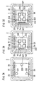
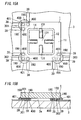
- Fig. 1A shows a top view of the module having the mounting structure of the chip in this embodiment.
- the arrowed line X indicates the right direction of the module.
- the arrowed line Y indicates the front direction of the module.
- the arrowed line Z is set perpendicular to both the arrowed line X and the arrowed line Y. That is, the arrowed line Z indicates the upper-lower direction of the module.
- Fig. 1B shows a side cross sectional view of the module having the mounting structure of the chip in this embodiment.
- the module in this embodiment comprises the substrate 3, the acceleration sensor 1, and the adhesive agents 2.
- the substrate 3 is made of material such as a ceramic and a glass epoxy resin.
- the substrate 3 is provided at its surface with a wiring which is omitted in the illustration.
- the substrate 3 comprises a base 31.
- the base 31 has "a base upper surface 3a".
- the base upper surface 3a is provided with a first arrangement spot 301, a second arrangement spot 302, and a third arrangement spot 303.
- the first arrangement sport 301, the second arrangement spot 302, and the third arrangement sport 303 are not arranged in a row. Therefore, the connecting lines of the first arrangement spot 301, the second arrangement spot 302, and the third arrangement spot 303 forms a triangle.
- first arrangement spot 301, the second arrangement spot 302, and the third arrangement spot 303 are positioned in vertexes of the triangle.
- Each one of the first arrangement spot 301, the second arrangement spot 302, and the third arrangement spot 303 is provided at its upper surface with the adhesive agent 2.
- the adhesive agent 2 is made of silicone series resin.
- the adhesive agents 2 comprises only the first adhesive agent 221, the second adhesive agent 222, and the third adhesive agent 223.
- the adhesive agent 2 further comprises a spherical-shaped spacer.
- the base 31 and the acceleration sensor 1 are arranged to leave the distance which is determined by the diameter of the spherical shaped spacer. Consequently, the acceleration sensor 1 is spaced from a base 31 to leave a predetermined distance.
- the spacer is preferably made of glass or plastic. In this case, it is possible to improve the accuracy of dimension of the spacer.
- the adhesive agent 2 further comprise the spacer having a dimension of 3 micrometers to 30 micrometers.
- the adhesive agent 2 comprises the silicone resin which contains 1 percent to 20 percents of spacer.
- the acceleration sensor defines the first chip.
- the acceleration sensor 1 has a rectangular shape. Therefore, the acceleration sensor 1 has an upper surface and a lower surface.
- the acceleration sensor 1 has a width and a length.
- the acceleration sensor 1 has a frame 11, a diaphragm 10, a weight 12, resistors Rx1, Rx2, Rx3, Rx4, resistors Ry1, Ry2, Ry3, Ry4, resistors Rz1, Rz2, Rz3, Rz4, and the first pad electrode 19.
- the frame 11 has a rectangular shape.
- the frame 11 is formed at its center with an opening which penetrates in the thickness direction of the frame 11. Therefore, the frame 11 has "an upper surface having a rectangular shape perpendicular to the thickness direction of the frame 11" and "a lower surface having a rectangular shape perpendicular to the thickness direction of the frame 11".
- the frame 11 is provided at outer periphery of the lower surface with a first side 141, a second side 142, a third side 143, and a fourth side 144.
- the first side 141 is opposite of the second side 142 in the lower surface of the frame 11.
- the third side 143 and the fourth side 144 are located adjacent to the first side 141, and also are located adjacent to the second side 142.
- the third side 143 is opposite of the fourth side 144 in the lower surface of the frame 11.
- the first end of the first side 141 is cooperative with the first end of the third side 143 to define the first adhesion spot 101.
- the second end of the first side 141 which is opposite of the first end of the first side 141 defines the second adhesion spot 102.
- One spot on the second side 142 defines the third adhesion spot 103. That is, the first adhesion spot 101, the second adhesion spot 102, and the third adhesion spot 103 are located in the periphery of the lower surface of the frame 11.
- the frame 11 has the upper surface.
- the diaphragm 10 is disposed on the upper surface of the frame 11.
- the diaphragm 10 is made of silicon. As will be understood from Fig. 1B , the diaphragm 10 is thinned. Therefore, the diaphragm 10 has flexibility.
- the diaphragm 10 has a dimension which is equal to the dimension of the frame 11.
- the diaphragm 10 comprises the frame portion 111, the beam 131, and the holding portion 121.
- the frame portion 111 has a thickness which is equal to the thicknesses of the four beams 131, and also equal to the thickness of the holding portion.
- the holding portion 121 is located in a center of the frame portion 111.
- Each one of the beams 131 has a first end which is coupled to the holding portion and a second end which is coupled to the inside circumferential surface of the frame portion 111.
- Each one of the beams 131 is spaced from the other of the beams 131. Consequently, the opening which is located in an inside of the frame portion 111 is divided by the beams 131 and the holding portion 121, whereby the opening is divided into four sub-openings.
- the holding portion 121 is provided at its lower surface with a weight 12.
- the holding portion 121 has a certain portion which is overlapped with respect to the holding portion 121 in the thickness direction.
- the weight 12 is held by the certain portion of the holding portion 121.
- the dimension of the plane which is perpendicular to the thickness direction of the weight 12 is set to be smaller than the dimension of the plane perpendicular to the thickness direction of the aperture of the frame 11. Consequently, the weight 12 is disposed within the frame 11 such that the weight 12 is spaced from the frame 11 by a gap 14.
- the gap 14 allows the weight to swing in the front-back direction and left-right direction according to the flexure of the beam 131.
- the flexure of the beam 131 allows the weight to swing in the upper-lower direction.
- the beam 131 which extends in the lateral direction has a connection portion which is connected to the holding portion 121.
- the connection portion is provided with the resistors Rx1, Rx2, Rx3, and Rx4.
- the resistors Rx1, Rx2, Rx3, and Rx4 are provided for detecting the acceleration in the X-axis direction.
- the beam 131 which extends in the front-back direction has a connection portion which is connected to the holding portion 121.
- the connection portion is provided with the resistors Ry1, Ry2, Ry3, and Ry4.
- the resistors Ry1, Ry2, Ry3, and Ry4 are provided for detecting the acceleration in the Y-axis direction.
- the frame portion 111 has a connection portion which is connected to the holding portion 121.
- the connection portion is provided with the resistors Rz1, Rz2, Rz3, and Rz4.
- the resistors Rz1, Rz2, Rz3, and Rz4 are provided for detecting the acceleration in the Z-axis direction.
- Each one of the resistors Rx1 to Rz4 is made of p-type semiconductor which comprises the silicon with dopant. That is, each the resistors Rx1 to Rx4 is realized by the piezoresistance.
- the resistors Rx1, Rx2, Rx3, and Rx4 are connected by the wiring which is not shown in the illustration such that the resistors Rx1, Rx2, Rx3, and Rx4 form the bridge circuit Bx shown in Fig. 2 .
- the resistors Ry1, Ry2, Ry3, and Ry4 are connected by the wiring which is not shown in the illustration such that the resistors Ry1, Ry2, Ry3, and Ry4 forms the bridge circuit By shown in Fig. 2 .
- the resistor Rz1, Rz2, Rz3, and Rz4 are connected by the wiring which is not shown in the illustration such that the resistors Rz1, Rz2, Rz3, and Rz4 form the bridge circuit Bz shown in Fig. 2 .
- each the bridge circuit Bx, By, and Bz are arranged in parallel with each other.
- the voltage is applied to each the bridge circuit Bx, By, and Bz through the input terminal VDD.
- each the bridge circuit Bx, By, and Bz has an output terminals X1, X2, Y1, Y2, Z1, and Z2.
- the input terminal VDD is connected to the output terminals X1 to Z2.
- the ground (earth) GND is connected to the first pad electrode 19 through a wiring which is not shown in the illustration.
- the first pad electrode 19 is connected to the power source in the outside, the voltage detection circuit, and the ground electrode (earth electrode) through the wiring which is not shown in the illustration.
- the voltage is applied to the input terminal VDD from the power source in the outside.
- the ground (earth) GND is connected to the ground electrode (earth electrode) in the outside.
- the output terminals Z1 to Z2 are connected to the voltage detection circuit in the outside.
- the voltage detection circuit is configured to detect the acceleration in the X-direction, Y-direction, and Z-direction according to the variation of the voltage output from the bridge circuit Bx, By, and Bz.
- the diaphragm 10 is provided at its periphery of the upper surface with a fifth side 145, a sixth side 146, a seventh side 147, and a eighth side 148.
- the fifth side 145 and the seventh side 147 extend in parallel with each other.
- the fifth side 145 is opposite of the first side 141 in the acceleration sensor.
- the fifth side 145 is aligned with the first side 141 in the thickness direction of the acceleration sensor 1.
- the sixth side 146 is opposite of the second side 142 in the thickness direction of the acceleration sensor 1.
- the sixth side 146 is aligned with the second side 142 in the thickness direction of the acceleration sensor 1.
- the seventh side 147 is opposite of the third side 143 in the thickness direction of the acceleration sensor 1.
- the seventh side 147 is aligned with the third side 143 in the thickness direction of the acceleration sensor 1.
- the eighth side 148 is opposite of the fourth side 144 in the thickness direction of the acceleration sensor 1.
- the eights side 148 is aligned with the fourth side 144 in the thickness direction of the acceleration sensor 1.
- the first pad electrodes 19 are arranged along the fifth side 145 on the upper surface of the diaphragm 10 such that the first pad electrodes 19 are located between the first arrangement spot 301 and the second arrangement spot 302. That is, all the first pad electrodes 19, the first arrangement spot 301, and the second arrangement spot 302 are arranged in the Y-direction of the acceleration sensor 1.
- the first pad electrode 19 comprises the input terminal VDD, the output terminals X1 to Z2, and the ground GND.
- the acceleration sensor 1 is attached to the base 31 through the adhesive agents on the first arrangement spot 301, the second arrangement spot 302, and the third arrangement spot 303. Consequently, the first arrangement spot 301 is faced to the first adhesion spot 101.
- the second arrangement spot 302 is faced to the second adhesion spot 102.
- the third arrangement spot 303 is faced to the third adhesion spot 103. Therefore, the first adhesive agent 221 is disposed on the first adhesion spot 301.
- the second adhesive agent 222 is disposed on the second adhesion spot 302.
- the third adhesive agent 223 is disposed on the third adhesion spot 303.
- the weight 12 When the acceleration sensor 1 is swung, the weight 12 is swung in the lateral direction defined by X-direction, the front-back direction defined by the Y-direction, and the upper-lower direction defined by the Z-direction.
- each the beam 131 When the weight 12 is swung, each the beam 131 is flexed.
- the stretching stress and the compression stress are caused to the beam 131.
- the stretching stress and the compression stress are applied to each the resistor Rx1 to Rz4.
- Each the resistor Rx1 to Rz4 is realized by the piezoresistance. Therefore, the resistance values of the resistors Rx1 to Rz4 is increased when the resistors Rx1 to Rz4 receives the stretching stress.
- the resistance value of the resistors Rx1 to Rz4 is decreased when the resistors Rx1 to Rz4 receive the compression stress.
- the resistance value of the bridge circuit Bx, By, and Bz are varied.
- the bridge circuit Bx, By, and Bz receives the voltage through the input terminal VDD. Therefore, the output voltage of the bridge circuit Bx, By, and Bz is varied according to the resistance value of the bridge circuit Bx, By, and Bz.
- the variation of the output voltage is detected by the voltage detection circuit. Then, the module detects the acceleration on the basis of the detection result.
- the acceleration sensor 1 is mounted on the base 31 as follows. At first, the adhesive agents 2 are applied to the first arrangement spot 301, the second arrangement spot 302, and the third arrangement spot 303 on the base upper surface 3a. Then, the acceleration sensor 1 is disposed on the adhesive agents 2. Consequently, the first arrangement spot 301 is faced to the first adhesion spot 101. The second arrangement spot 302 is faced to the second adhesion spot 102. The third arrangement spot 303 is faced to the third adhesion spot 103. Consequently, the substrate 3, the adhesive agent 2, and the acceleration sensor 1 are arranged in the manner shown in Fig. 3A . The substrate 3, the adhesive agent, and the acceleration sensor 1 are heated at 150 degrees.
- the adhesive agent, and the acceleration sensor 1 are heated, the warpage of the substrate 1 is caused. Then, the substrate 3 is cooled to a room temperature. Consequently, the acceleration sensor 1 is adhered to the base 31 having warpage through the adhesive agents 2. However, the acceleration sensor 1 is adhered to the substrate 3 through the three points of the first adhesive agent 221, the second adhesive agent 222, and the third adhesive agent 223. Therefore, even if the stress is caused by changing from the warpage condition to the flat condition of the base 31, the acceleration sensor 1 is fixed to the base 31 such that the acceleration sensor 1 is made inclination with respect to the base 31. Consequently, the stress is released. However, the inclination is nanometer-level. Therefore, the inclination causes no effect with respect to the detection accuracy of the acceleration sensor 1.
- the mounting structure of chip in this embodiment makes it possible to prevent the semiconductor device such as the acceleration sensor from being made deformation due to the warpage of the substrate. Therefore, it is possible to obtain the acceleration sensor which is free from the effect of the stress after the chip is mounted on the substrate.
- all the first pad electrodes 19 are arranged along the fifth side 145 such that all the first pad electrodes 19 are located between the first adhesion spot 101 and the second adhesion spot 102. That is, the first pad electrodes 19 are arranged along the fifth side 145 such that the first pad electrodes 19 are located between the first adhesive agent 221 and the second adhesive agent 222. The first pad electrodes 19 are arranged along the fifth side 145 which is spaced away from the third adhesive agent 223. Consequently, even if the stress is applied to the first pad electrodes 19 from the upside, the acceleration sensor 1 is stably supported by the substrate 3. Therefore, it is possible to establish the bonding of the first pad electrodes by the bonding wire.
- the adhesive agent 2 is made of silicone-series resin.
- the silicone-series resin has a low coefficient of elasticity. Therefore, the adhesive agent 2 made of the silicone series resin absorbs the stress applied to the acceleration sensor 1 from the substrate.
- the adhesive agents 2 are disposed on the three spots of the substrate such that the adhesive agents 2 cover the lower side of the outer circumference of the acceleration sensor. Therefore, it is possible to prevent the acceleration sensor 1 from being come off when the acceleration sensor 1 receives the force in the front-back direction and the lateral direction.
- Fig. 4A show a top view of the module having the mounting structure of chip in the first modification of this embodiment.
- Fig. 4B shows a side cross sectional view of the module having the mounting structure of chip in the modification of this embodiment.
- the first adhesion spot 101 is defined by the first end of the first side 141 and the first end of the third side 143.
- the second adhesion spot 102 is defined by the second end, opposite of the first end, of the first side 141.
- the third adhesion spot 103 is defined by the second end, opposite of the first end, of the third side 143.
- all the first pad electrodes 19 comprises a first electrode row and a second electrode row.
- the first electrode row is arranged along the fifth side 145. Therefore, the first electrode row is arranged in the Y-direction of the acceleration sensor 1 such that the first electrode row is located between the first adhesive agent 221 and the second adhesive agent 222.
- the second electrode row is arranged along the seventh side 147. Therefore, the second electrode row is arranged along the X-direction of the acceleration sensor 1 such that the second electrode row is located between the first adhesive agent 221 and the third adhesive agent 223.
- the mounting structure of chip in this configuration also makes it possible to establish the stable bonding of the bonding wire with respect to each the first pad electrode 19.
- the arrangement of the adhesive agent 2 is not limited to the arrangement in the first embodiment and the modification of the first embodiment.
- the arrangement of the adhesive agent 2 of (a) to (I) shown in Fig. 5 also makes it possible to achieve the effect of the above.
- the longitudinal row A of Fig. 5 shows all the adhesive agents 2 which are disposed in the three corners of the lower surface of the acceleration sensor 1.
- the longitudinal row B of Fig. 5 shows two adhesive agents 2 which are disposed in two corners of the lower surface of the acceleration sensor 1.
- the longitudinal row C of Fig. 5 shows one adhesive agent 2 which is disposed in one corner of the lower surface of the acceleration sensor.
- the longitudinal row D in Fig. 5 shows the adhesive agents 2 any one of which is disposed in corner of the acceleration sensor 1.
- the adhesive agents 2 are disposed such that the triangle has a large dimension and the center of the triangle is located in a center of the semiconductor element.
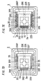
- Fig. 16 shows the module of the mounting structure of chip in the second modification of this embodiment.
- the base 31 is provided with the projections 900 which are located in the first arrangement spot 301, the second arrangement spot 302, and the third arrangement spot 303, respectively.
- the projections 90 are located between "the arrangement spot 301 and the adhesion spot 101", between " the arrangement spot 302 and the adhesion spot 102", and between "the arrangement spot 303 and the adhesion spot 103", respectively.
- the projections 900 are covered by the first adhesive agent 221, the second adhesive agent 222, and the third adhesive agent 223.
- each one of the first adhesive agent 221, the second adhesive agent 222, and the third adhesive agent 223 are located between "the upper surfaces of the projections" and "the lower surface of the frame 11". Consequently, even if the stress is caused when the base 31 is changed from the warpage condition into the flat condition, it is possible to release the stress. Furthermore, it is possible to leave a space between the base upper surface 3a and the lower surface of the acceleration sensor by a uniform distance.
- the explanation of the above embodiment is made with using the first chip which is defined by the acceleration sensor 1 of piezoresistance type.
- the first chip is not limited to the acceleration sensor of the piezoresistance type. That is, the mounting structure of chip of the above may be applied to "a MEMS device such as acceleration sensor of capacitance type, a gyro sensor, a pressure sensor, a micro-actuator, a micro-relay, a micro-valve, an infrared sensor", and "the module such as IC chip”.
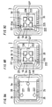
- Fig. 6A shows a top view of the module in this embodiment.
- Fig. 6B shows a side cross sectional view of this embodiment.
- the module in this embodiment comprises the substrate 3B, the adhesive agent 2, the acceleration sensor 1, the adhesive agent 20, and the IC chip 200.
- the substrate 3B is made of material such as a ceramic and a glass epoxy resin.
- the substrate 3 is formed to have the base 31, the step 32, and the peripheral wall 33.
- the step 32 extends toward the upper direction from the periphery of the base 31.
- the peripheral wall 33 extends toward the upper direction from the periphery of the base 31 and the step 32. Consequently, the substrate 3B has a box shape and is provided at its upper surface with an opening.
- the peripheral wall 33 is provided at its upper end with the adhesive agents 34.
- the lid is attached to the peripheral wall 33 through the adhesive agent 34.
- the step 32 has an upper surface which is defined as "a step upper surface 32f'. "The step upper surface 32f' has a first height from "the base upper surface 3a”.
- the step upper surface 32f is provided with a plurality of the wirings 35.
- the adhesive agent 2 comprises the silicone series resin 2a mixed with the spacers 2b having the spherical shapes.
- the acceleration sensor 1 is cooperative with the IC chip 200 to construct the semiconductor device.
- the acceleration sensor 1 has an upper surface which is defined as "a sensor upper surface 2S", and is provide at its sensor upper surface 2S with the fourth arrangement spot 104, the fifth arrangement spot 105, the sixth arrangement spot 106, and a plurality of the first pad electrodes 19.
- the fourth arrangement spot 104, the fifth arrangement spot 105, and the sixth arrangement spot 106 are not arranged in a row. Therefore, the connecting lines of the fourth arrangement spot 104, the fifth arrangement spot 105, and the sixth arrangement spot 106 forms a triangle.
- the fourth arrangement spot 104 is aligned with the first adhesion spot 301 in the thickness direction of the acceleration sensor 1.
- the fifth arrangement spot 105 is aligned in the second adhesion spot 302 in the thickness direction of the acceleration sensor 1. Therefore, the fifth arrangement spot 105 and the sixth arrangement spot 106 are located in the first end in the longitudinal direction of the acceleration sensor 1.
- the fifth arrangement spot 105 and the sixth arrangement spot 106 are located in one end in the width direction and the other end in the width direction of the acceleration sensor 1, respectively.
- the sixth arrangement spot 106 is aligned with the third adhesion spot 303 in the thickness direction of the acceleration sensor 1.
- a plurality of the first pad electrodes 19 are arranged along the fifth side 145 such that a plurality of the first pad electrodes 19 are located between the fourth arrangement spot 104 and the fifth arrangement spot 105.
- the adhesive agent 20 is made of silicone series resin 20a mixed with the spacers 20b having spherical shapes.
- the adhesive agent 20 comprises the fourth adhesive agent 224, the fifth adhesive agent 225, and the sixth adhesive agent 226.
- the adhesive agents 20 are only applied to the fourth spot 104, the fifth spot 105, and the sixth spot 106.
- the IC chip 200 is defined as the second chip.
- IC chip 200 has a rectangular shape.
- IC chip 200 has "an IC chip lower surface 20u which is faced to the sensor upper surface 2S" and "an IC chip upper surface 20S which is opposite of the IC chip lower surface 20u".
- the IC chip 200 is provided at its IC chip lower surface 20u with the fourth adhesion spot 304, the fifth adhesion spot 305, and the sixth adhesion spot 306.
- the IC chip 200 is disposed on the upper surface of the acceleration sensor 1 such that all the first pad electrodes 19 are exposed to the upper direction of the acceleration sensor 1.
- the IC chip 200 is disposed on the upper side of the acceleration sensor 1. Consequently, the fourth arrangement spot 104 is faced to the fourth adhesion spot 304.
- the fifth arrangement spot 105 is faced to the fifth adhesion spot 305.
- the sixth arrangement spot 106 is faced to the sixth adhesion spot 306. Consequently, the lower surface of the IC chip 200 is located at a second height from the base upper surface 3a. The second height is set to be greater than the first height.
- the IC chip 200 has one longitudinal end defined as the first end and the other longitudinal end defined as the second end.
- the first end of the IC chip 200 is defined as an overlapping portion 200P.
- the second end of the IC chip 200 has the fourth adhesion spot 304 and the fifth adhesion spot 305.
- the fourth adhesion spot 304 is disposed in one width end of the lower surface of the IC chip 200 and the fifth adhesion spot 305 is disposed in the other width end of the lower surface of the IC chip 200. Therefore, the overlapping portion 200P has the lower surface which is located at a second height from the base upper surface 3a.
- the IC chip 200 is disposed on the same side of the acceleration sensor 1 as the upper surface of upper surface of the acceleration sensor 1 such that the overlapping portion 200P is overlapped with the step upper surface 32f.
- the IC chip 200 has a length which is greater than a length of the acceleration sensor 1.
- the IC chip 200 is provided at its IC chip upper surface 20S with "a plurality of the second pad electrodes 202" and "a plurality of the third pad electrodes 203". All the second pad electrodes 202 are disposed along one side of the IC chip upper surface 20S such that all the second pad electrodes 202 are located between the fourth adhesion spot 304 and the fifth adhesion spot 305.
- the second pad electrodes 202 are electrically connected to the first pad electrodes 19 through the bonding wires 15, respectively.
- the second electrode pads 202 are connected to the third electrode pads 203, respectively, through the wirings not shown in the illustration.
- the third pad electrodes 203 are arranged in a plurality of the sides of the IC chip upper surface 20S such that the third pad electrodes 203 are arranged in parallel with a plurality of the wirings 35 of the substrate 3B.
- the third pad electrodes 203 are electrically connected to the wirings 35, respectively, through the bonding wires 215.
- the wiring 35 is connected to the voltage source disposed in the outside.
- the acceleration sensor 1 is connected to the power source provided in the outside.
- the IC chip is configured to calculate the acceleration on the basis of the voltage signal sent from the second pad electrodes 202.
- the IC chip is configured to output a signal indicative of the acceleration to the through the third pad electrode.
- the above acceleration sensor 1 and the IC chip 200 are mounted on the substrate 32 as follows. Firstly, as shown in Fig. 7A , the adhesive agents 2 are applied to the first arrangement spot 301, the second arrangement spot 302, and the third arrangement spot 303 of the base upper surface 3a. Then, the acceleration sensor 1 is disposed on the upper surface of the adhesive agent 2. Consequently, the first arrangement spot 301 is faced to the first adhesion spot 101. The second arrangement spot 302 is faced to the second adhesion spot 102. The third arrangement spot 303 is faced to the third adhesion spot 103. Consequently, as shown in Fig. 7B , the substrate 3, the adhesive agent 2, and the acceleration sensor 1 are arranged. The substrate 3, the adhesive agent 2, and the acceleration sensor 1 are heated at 150 degrees C.
- the acceleration sensor 1 is adhered to the substrate 3 having the warpage through the adhesive agent 2.
- the acceleration sensor 1 is adhered to the substrate 3 through the three points of the first adhesive agent 221, the second adhesive agent 22, and the third adhesive agent 223. Therefore, even if the stress is caused when the substrate 3 is changed from the warpage condition into the flat condition, the acceleration sensor 1 is fixed to the substrate such that the acceleration sensor is made inclination with respect to the substrate. Therefore, the inclination releases the stress.
- the inclination is nanometer level. Therefore, the inclination causes no effect of the detection accuracy of the acceleration sensor 1.
- the acceleration sensor 1 is attached to the substrate 3 under a condition shown in Fig. 7B .
- the adhesive agent 20 is applied to the fourth arrangement spot 104, the fifth arrangement spot 105, and the sixth arrangement spot 106 of the sensor upper surface 2S.
- the IC chip 200 is disposed on the same side of the acceleration sensor 1 as the upper surface of the acceleration sensor 1. Consequently, the fourth arrangement spot 104 is faced to the fourth adhesion spot 304.
- the fifth arrangement spot 105 is faced to the fifth adhesion spot 305.
- the sixth arrangement spot 106 is faced to the sixth adhesion spot 306.
- the first pad electrodes 19 are exposed to the upper side of the acceleration sensor 1.
- the overlapping portion 200P is overlapped with the step upper surface 32f.
- the substrate 3, the adhesive agent 2, the acceleration sensor 1, the adhesive agent 20, and the IC chip 200 are heated at 150 degrees C.
- the acceleration sensor 1 has a linear coefficient of expansion which is different from a linear coefficient of expansion of the IC chip 200. Therefore, the warpage of the acceleration sensor 1 is different from the warpage of the IC chip 200.
- the substrate 3, the adhesive agent 2, and the acceleration sensor 1 is cooled to the room temperature, the IC chip 200 is adhered to the acceleration sensor 200 under a condition where the IC chip 200 is inclined with respect to the acceleration sensor 1. Therefore, the stress caused by the warpage of the IC chip 200 is released. Consequently, similar to the above, the acceleration sensor 1 is mounted on the substrate 3 without receiving the stress from the IC chip 200.
- the components have the arrangement shown in Fig. 7D .
- the first pad electrodes 19 are electrically connected to the second pad electrodes 202 through the wires 15.
- the third pad electrodes 203 are electrically connected to the wiring through the wire 215.
- the modules are operated as follows.
- the module receives the voltage from the voltage source in the outside of the module.
- the voltage is applied to the input terminal VDD of the first pad electrodes 19 through the third pad electrodes. Consequently, each the piezoresistances Rx1 to Rz4 receives the voltage.
- Each the piezoresistances outputs the voltage signal from the output terminal X1 to Z2 of the first pad electrodes 19.
- IC chip 200 receives the output signal through the wire 15 and the second pad electrode 202.
- the IC chip 200 comprises the voltage detection circuit.
- the IC chip 200 calculates the acceleration on the basis of the output signal, and outputs the signal indicative of the acceleration through the third pad electrode 203, the wire 215, and the wiring 35.
- the module with the mounting structure of chip of the above comprises the semiconductor device comprising the acceleration sensor 1 and the IC chip 200.
- the semiconductor device is mounted on the base 31 through the first adhesive agent 221, the second adhesive agent 222, and the third adhesive agent 223 on the base upper surface 3a.
- the IC chip 200 is mounted on the acceleration sensor 1 through the fourth adhesive agent 224, the fifth adhesive agent 225, and the sixth adhesive agent 226 on the upper surface of the acceleration sensor 1.
- the first adhesive agent 221 is aligned with the fourth adhesive agent 224 in the thickness direction of the acceleration sensor 1.
- the second adhesive agent 222 is aligned with the fifth adhesive agent 225 in the thickness direction of the acceleration sensor 1.
- the third adhesive agent 223 is aligned with the sixth adhesive agent 226 in the thickness direction of the acceleration sensor 1.
- the adhesive agents 2 are aligned with the adhesive agents 20, respectively, in the thickness direction of the acceleration sensor 1. Therefore, it is possible to prevent the deformation of the acceleration sensor 1 due to the warpage caused in a situation where the acceleration sensor 1 is mounted on the substrate 1. Therefore, the mounting structure of chip in this embodiment makes it possible to produce the semiconductor device which is free from the stress after mounting on the substgrate.
- the adhesive agent 20 is made of silicone series resin.
- the silicone series resin has a low coefficient of elasticity. Therefore, the adhesive agent 20 made of silicone series resin makes it possible to prevent the transfer of the stress to the IC chip 200 through the acceleration sensor 1 from the substrate 3.
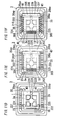
- Fig. 8 shows the module in the first modification of this embodiment.
- the module in this modification further comprises the seventh adhesive agent 40.
- the seventh adhesive agent 40 is located between the step upper surface 32f and the lower surface of the overlapping portion 200P. Consequently, the seventh adhesive agent 40 bonds the step upper surface 32f to the overlapping portion 200P.
- the acceleration sensor 1 and the IC chip 200 are mounted on the substrate 3 as follows. Firstly, as shown in Fig. 9A , the adhesive agents 2 are applied to the first arrangement spot 301, the second arrangement spot 302, and the third arrangement spot 303 on the base upper surface 3a. Then, the acceleration sensor 1 is disposed on the upper surface of the adhesive agents 2. Consequently, the first arrangement spot 301 is faced to the first adhesion spot 101. The second arrangement spot 302 is faced to the second adhesion spot 102. The third arrangement spot 303 is faced to the third adhesion spot 103. Consequently, the substrate 3, the adhesive agents 2, and the acceleration sensor 1 have an arrangement shown in Fig. 9 B. The substrate 3, the adhesive agent 2, and the acceleration sensor 1 are heated at 150 degrees C.
- the acceleration sensor 1 is adhered to the substrate 3 having the warpage through the adhesive agent 2.
- the acceleration sensor 1 is adhered to the substrate 3 through only the first adhesive agent 221, the second adhesive agent 222, and the third adhesive agent 223. Therefore, even if the stress is caused when the substrate 3 is changed from the warpage condition into the flat condition, the acceleration sensor 1 is fixed to the substrate under a condition where the acceleration sensor 1 has an inclination with respect to the substrate. The inclination causes the release of the stress. In addition, the inclination is nanometer level. Therefore, the inclination causes no effect of the detection accuracy of the acceleration sensor 1. Furthermore, the acceleration sensor is fixed to the substrate 3 to have a condition shown by Fig. 9B .
- the adhesive agents 20 are applied to the fourth spot 104, the fifth spot 105, and the sixth spot 106 on the sensor upper surface 2S.
- the IC chip 200 is mounted on the same side of the acceleration sensor 1 as the upper surface of the acceleration sensor 1. Consequently, the fourth arrangement spot 104 is faced to the fourth adhesion spot 304.
- the fifth arrangement spot 105 is faced to the fifth adhesion spot 305.
- the sixth arrangement spot 106 is faced to the sixth adhesion spot 306.
- the first pad electrodes 19 are exposed to the upper direction of the acceleration sensor 1.
- the overlapping portion 200P is located in a position such that the overlapping portion 200P is spaced from the step upper surface 32f to leave the gap 41.
- the substrate 3, the adhesive agent 2, the acceleration sensor 1, the adhesive agent 20, and the IC chip 200 are heated at 150 degrees C. Consequently, similar to the above, the acceleration sensor 1 and the IC chip 200 are mounted on the substrate 3 without receiving the stress from the substrate 3. Consequently, the components have an arrangement shown in Fig. 9D . Then, the gap 41 is filled with the seventh adhesive agent 40. Then, the substrate 3, the adhesive agent 2, the acceleration sensor 1, the adhesive agent 20, the IC chip 200, and the seventh adhesive agent 40 are heated at 150 degrees C. Consequently, the overlapping portion 200P is adhered to the step upper surface 32f. Then, as shown in Fig. 9F , the first pad electrodes 19 is electrically connected to the second pad electrodes 202 through the wires 15. The third pad electrodes 203 are electrically connected to the wiring through the wire 215.
- the module with mounting structure of chip comprises the IC chip 200 which has an overlapping portion 200P.
- the IC chip 200 is disposed on the upper side of the substrate 3B and on the upper side of the acceleration sensor 1 such that the gap 41 is left between the overlapping portion 200P and the step upper surface 32f.
- the gap 41 is filled with the seventh adhesive agent 40. Therefore, it is possible to stably establish the wire bonding with respect to the second pad electrodes 202.
- Fig. 10 shows a second modification of this embodiment.
- the lower surface of the overlapping portion 200P is provided at its both width ends of the acceleration sensor 1 with an overlapping spots 20ap, 20bp. Consequently, the overlapping spots 20ap, 20bp are located in two corners of the IC chip 200.
- the step upper surface 32f is provided with the arrangement spots 30ap, 30bp which are faced to the overlapping spots 20ap, 20bp, respectively.
- the seventh adhesive agents 40 are preferably disposed such that the seventh adhesive agents 40 are located between "the overlapping spot 20ap and the arrangement spot 30a", and between "the overlapping spot 20bp and the arrangement spot 30a", respectively.
- the module with mounting structure of chip in the third embodiment of this invention is explained with attached drawings. It is noted that the components in this embodiment in common with the components in the first embodiment are symbolized by the same reference numerals, whereby the explanation is omitted. As will be understood from Fig. 12 and Fig. 13 , the module in this embodiment comprises the substrate 3, the bump 400, and the acceleration sensor 1.
- the substrate 3 further comprises a plurality of wirings 39.
- a plurality of the wirings 39 is disposed on the upper surface of the substrate 3.
- One end of each the wiring acts as a connecting electrode.
- the connecting electrodes are located in the first arrangement spot 301 or the second arrangement spot 302 or the third arrangement spot 303.
- the connecting electrodes are provided at its upper surface with bumps 400, respectively.
- the bump 400 acts as the adhesive agent.
- the bump 400 is made of a solder.
- the bump 400 is disposed on the upper surface of one end of each the wiring 30. That is, the bumps 400 are disposed on the first arrangement spot 301, the second arrangement spot 302, and the third arrangement spot 303, respectively.
- the acceleration sensor 1 B further comprises a plurality of terminal electrodes 190.
- the terminal electrodes 190 are located on the first adhesion spot 101, the second adhesion spot 102, and the third adhesion spot 103, respectively. Further, as shown in Fig. 12A , the acceleration sensor 1 is disposed on the upper surface of the substrate 3 such that each the terminal electrode 190 is faced to the connecting electrode on one end of each the wiring 39.
- the input terminal VDD, the output terminal X1 to Z2, and the ground (earth) GND are connected to each the terminal electrode 190 via the wiring in the through hole which penetrates the frame 11 and which extends in the thickness direction of the frame 11.
- Each the terminal electrode 190 is connected to the power source in the outside of the module, the voltage detection circuit, and the ground electrode (earth electrode) through the wiring which is not shown in the illustration.
- the power source in the outside of the module is configured to apply the voltage to the input terminal VDD.
- the ground (earth) GND is connected to the ground electrode (earth electrode) in the outside of the module.
- the output terminal Z1 to Z2 is connected to the voltage detection circuit in the outside of the module.
- the voltage detection circuit is configured to detect the accelerations in X-direction, Y-direction, and Z-direction on the basis of the variation of the voltage which is output from the bridge circuit Bx, By, and Bz.
- the acceleration sensor 1 is mounted on the substrate 3 as follows. Firstly, as will be understood from Fig. 14A , the bump 400 is provided to the lower surface of each the terminal electrode 190. Then, the acceleration sensor 1 is disposed on the supper surface of the substrate 3 such that "the connecting electrode in one end of each the wiring 39", "each the bump 400", and “each the terminal electrode 190" are aligned with each other in the thickness direction of "the substrate 3 and the acceleration sensor 1". Then, the substrate 3, the bump 400, and the acceleration sensor 1 are heated at a predetermined temperature. When the substrate 3, the bump 400, and the acceleration sensor 1 are heated, as shown in Fig. 14B , the heat causes the warpage of the substrate.
- the substrate 3, the bump 400, and the acceleration sensor 1 are cooled to a room temperature. Consequently, the acceleration sensor 1 is bonded to the substrate having the warpage through the bump 400. However, the acceleration sensor 1 is adhered to the substrate 3 through only three spots. Therefore, when the substrate 3 is changed from the warpage condition into flat condition, the stress is caused. However, the acceleration sensor 1 is fixed to the substrate such that the acceleration sensor 1 has an inclination with respect to the substrate 3. This inclination releases the stress. In addition, this inclination is nanometer level. Therefore, the inclination causes no effect to the detection accuracy of the acceleration sensor 1.
- the module with mounting structure of chip in this embodiment of this embodiment makes it possible to prevent the warpage of the substrate when mounting the first chip. Therefore, it is possible to prevent the deformation of the first chip. Consequently, it is possible to obtain the module with the first chip which is free from the stress after mounting on the substrate.
- Fig. 15 shows a first modification of this embodiment.
- the module in this modification further comprises an encapsulation resin 401.
- the encapsulation resins 401 are located in positions "between the first arrangement spot 301 and the first adhesion spot 101", "between the second arrangement spot 302 and the second adhesion spot 102", and "between the third arrangement spot 303 and the third adhesion spot 103". Consequently, the encapsulation resins 401 encapsulate the bumps 400.
- the acceleration sensor 1 is mounted on the substrate 3 as follows. Firstly, the bump 400 and the encapsulation resin 401 are formed on the lower surface of each the terminal electrode 190. Then, the acceleration sensor 1 is disposed on the upper surface of the substrate 3 such that "one end of each the wiring 39", "each the bump 400", and “each the terminal electrode 190" are aligned with each other in the thickness direction of "the substrate 3 and the acceleration sensor 1". Then, the substrate 3, the bump 400, and the acceleration sensor 1 are heated to a predetermined temperature. When the substrate 3, the bump 400, and the acceleration sensor 1 are heated, as shown in Fig. 14 B, the heat causes the warpage of the substrate 3. Then, the substrate 3, the bump 400, and the acceleration sensor 1 are cooled at room temperature.
- the acceleration sensor 1 is adhered to the substrate 3 with the warpage through the bump 400.
- the acceleration sensor 1 is adhered to the substrate 3 through the three spots.
- the stress is caused.
- the acceleration sensor 1 is fixed to the substrate such that the acceleration sensor 1 has an inclination with respect to the substrate. Therefore, the stress is released by the inclination.
- the encapsulation resin 401 is located between each the arrangement spot and each the adhesion spot. Therefore, it is possible to stably establish the electrical connection of the bump 400 with respect to the terminal electrode 190.
- the module with mounting structure of chip in this modification makes it possible to prevent the contact failure of the bump 400 with respect to one end of the wiring 39 when the substrate is changed from the warpage condition into the flat condition under a condition where the acceleration sensor 1 is mounted.
- a plurality of the bumps 400 are disposed on the first arrangement spot 301, are disposed on the second arrangement spot 302, and are disposed on the third arrangement spot 303.
- this embodiment discloses the bump 400 which is made of the solder.
- the bump 400 is not limited its material to the solder.
- the bump made of metal material such as Au may be employed as the bump.
- it is possible to employ the bump made of the electrical conductive paste of silicone series resin may be employed as the bump.
- the bump made of electrical conductive paste having the silicone series resin it is possible to reduce the effect to the acceleration sensor 1 due to the stress caused by the temperature variation of the substrate.
- the bump made of the electrical conductive paste of silicone series resin it is possible to establish the stable connection of the bump with respect to the terminal electrode 190.
Landscapes
- Physics & Mathematics (AREA)
- General Physics & Mathematics (AREA)
- Engineering & Computer Science (AREA)
- Microelectronics & Electronic Packaging (AREA)
- Computer Hardware Design (AREA)
- Pressure Sensors (AREA)
Abstract
Description
- This invention relates to a mounting structure of the chip comprising a substrate, a chip which is realized by the semiconductor device and which is disposed on the upper surface of the substrate, and the adhesive agent for bonding the substrate and the chip. In addition, this invention relates to a module comprising the mounting structure of chip.
- Japanese patent application publication No.
2006-133123A - The acceleration sensor is assembled as follows. Firstly, the adhesive agent is applied to the four arrangement spots of the substrate. Subsequently, the acceleration sensor is disposed on the upper surface of the substrate through each the adhesive agent such that each the arrangement spot is faced to the adhesive portion. The substrate, the adhesive agents, and the acceleration sensor are heated at, for example, 150 degree C. When the adhesive agents are heated, the acceleration sensor and the substrate are bonded by the adhesive agent. Then, the substrate, the adhesive agent, and the acceleration sensor are cooled to room temperature. In this manner, the acceleration sensor is assembled.
- However, when the substrate, the adhesive agent, and the acceleration sensor are heated to 150 degree C, the substrate is changed into a warpage condition from a normal condition. Then, the acceleration sensor and the substrate which has the warpage are bonded by the adhesive agent. Subsequently, when the substrate having the warpage, the adhesive agent, and the acceleration sensor are cooled to the room temperature, the substrate is changed into the normal condition from the warpage condition. However, the acceleration sensor and the warped substrate are bonded by the adhesive agent. Therefore, when the substrate is changed into the normal condition from the warpage condition, the acceleration sensor receives the stress.
- This invention is produced to solve the above problem. A first objective of this invention is to produce a mounting structure of chip which is configured to reduce the stress applied to the chip. In addition, a second objective of this invention is to produce the module having the mounting structure of chip of the above.
- In order to solve the above problem, this invention discloses a mounting structure of chip which comprises a substrate having a base, a first chip disposed on an upper surface of the base, and adhesive agents which is configured to bond the first chip to the base. The adhesive agents are disposed on the upper surface of the base. The first chip is shaped to have a rectangular shape, whereby the first chip has a width and a length. The first chip is bonded at its lower surface to the base by the adhesive agents. The adhesive agents comprise only the first adhesive agent, the second adhesive agent, and the third adhesive agents. The first adhesive agent, the second adhesive agent, and the third adhesive agents are disposed on the three spots of the upper surface of the base, respectively. The three spots of the upper surface of the base are not arranged in a row. Therefore, when the three spots of the upper surface of the base are connected by the connecting lines, the connecting lines form the triangle. Therefore, the three spots of the upper surface of the base have arrangement such that the three spots are located in the vertexes of the triangle which is formed by the connecting lines which connects the three spots with each other. The first chip is bonded to the base by only the first adhesive agent, the second adhesive agent, and the third adhesive agent.
- When the first chip is mounted on the substrate, the substrate is deformed according to the increase of the temperature. Then, the substrate is changed into normal condition when the substrate is cooled to the room temperature. However, the above configuration makes it possible to prevent the first chip from receiving the stress due to the deformation caused by the temperature variation of the substrate.
- The first chip further comprises a plurality of the first pad electrodes. The first pad electrodes are disposed on the upper surface of the first chip. "The first adhesive agent and the second adhesive agent" are located in one lengthwise end of the first chip, and "the third adhesive agent" is located in a remaining lengthwise end of the first chip, the remaining lengthwise end of the first chip is opposite of the one lengthwise end of the first chip. The first adhesive agent is located in one width end of the first chip and the second adhesive agent is located in a remaining width end of the first chip, the remaining width end of the first chip is opposite to the one width end of the first chip. All the first pad electrodes are arranged in the width direction on the upper surface of the first chip such that all said first pad electrode is located between the first adhesive agent and the second adhesive agent. In addition, all the first pad electrodes are located in the one lengthwise end of the first chip, the one lengthwise end of the first chip is located away from the third adhesive agent.
- In this case, it is possible to make a bonding of the bonding wires to the first pad electrodes, respectively.
- In addition, the first chip further comprises a plurality of the first pad electrodes. A plurality of the first pad electrodes are disposed on the upper surface of the first chip. "The first adhesive agent and the second adhesive agent" are located in one lengthwise end of the first chip, and the third adhesive agent is located in a remaining lengthwise end of the first chip. The remaining lengthwise end of the first chip is opposite of the one lengthwise end of the first chip. The first adhesive agent is located in one width end of the lower surface of the first chip and the second adhesive agent is located in a remaining width end of the lower surface of the first chip. The remaining width end of the lower surface of the first chip is opposite of the one width end of the lower surface of the first chip. A plurality of the first pad electrodes comprises a first electrode row and a second electrode row. The first electrode row, the first adhesive agent, and the second adhesive agent are arranged in the width direction of the first chip. The second electrode row, the first adhesive agent, and the third adhesive agent are arranged in the length direction of the first chip.
- In this case, it is possible to make a stable bonding of each the bonding wire with respect to each the first pad electrode.
- It is preferred that the module has above mentioned mounting structure of chip. The module comprises a second chip, a fourth adhesive agent, a fifth adhesive agent, and a sixth adhesive agent in addition to the substrate, the first chip, the first adhesive agent, the second adhesive agent, and the third adhesive agent. The fourth adhesive agent, the fifth adhesive agent, and the sixth adhesive agent are disposed on only the three spots of the upper surface of the first chip, respectively. The three spots of the upper surface of the first chip are not arranged in a straight line. Therefore, the connecting lines which connect the three spots of the upper surface of the first chip with each other forms a triangle. Therefore, the three spots of the upper surface of the first chip have an arrangement such that the three spots are located in the vertexes of the triangle which is formed by the connecting line which connects the three points with each other. The first chip has a plurality of the first pad electrodes. The pad electrodes are disposed on the upper surface of the first chip. The second chip is bonded to the first chip by the fourth adhesive agent, the fifth adhesive agent, and the sixth adhesive agent such that all the first pad electrode are exposed to the upper direction.
- The second chip has a linear coefficient of expansion which is different from a linear coefficient of expansion of the first chip. Therefore, the second chip is greatly deformed according to the temperature increase of the second chip when the second chip is mounted on the first chip. In addition, when the second chip is cooled to the room temperature, the second chip is changed into the flat condition. However, this configuration makes it possible to bond the second chip to the first chip under a condition where the second chip has an inclination with respect to the first chip. The inclination releases the stress due to the deformation caused by the temperature variation of the second chip.
- The first adhesive agent is preferably aligned with the fourth adhesive agent in the thickness direction of the first chip. Similarly, it is preferred that the second adhesive agent is aligned with the fifth adhesive agent. Similarly, the sixth adhesive agent is preferably aligned with the sixth adhesive agent.
- In this case, it is possible to stably adhere the second chip to the upper surface of the first chip.
- The substrate preferably comprises a step and a peripheral wall. The step extends in the upper direction from the outer end of the base. The step has "a step upper surface". The step upper surface has a first height from the upper surface of the base. The peripheral wall extends to the upper direction from an entire circumference of the base and the step such that the peripheral wall surrounds the base and the step. The second chip has a rectangular shape, whereby the second chip has a width and a length. The second chip has one lengthwise end and a remaining lengthwise end opposite of the one lengthwise end. The one lengthwise end of the lengthwise end of the second chip is defined as the overlapping portion. The remaining lengthwise end of the second chip is bonded to the first chip by the fourth adhesive agent and the fifth adhesive agent. The overlapping portion has a lower surface having a second height from the upper surface of the base. The second height is greater than the first height. The second chip is disposed on the upper surface of the first chip such that the overlapping portion is overlapped with the step upper surface. The module further comprises the seventh adhesive agent. The seventh adhesive agent is disposed between "the lower surface of the overlapping portion" and the step upper surface. The seventh adhesive agent is configured to bond the lower surface of the overlapping portion to the step upper surface.
- In this case, it is possible to make a stable wire bonding with respect to the upper surface of the second chip.
- It is preferred that the four adhesive agent is located in one width end of the second chip, and the fifth adhesive agent is located in a remaining width end of the second chip. The remaining width end of the second is opposite of the one width end of the second chip.
- In this case, it is possible to make a stable wire bonding with respect to the upper surface of the second chip.
- The seventh adhesive agent is preferably located in the one width end of the second chip and the remaining width end of the second chip such that the seventh adhesive agent is located in two corners of the second chip.
- In this case, it is possible to make a stable wire bonding with respect to the upper surface of the second chip.
- The substrate preferably comprises the connecting electrodes. The connecting electrodes are disposed on the three spots of the substrate. The first chip has a plurality of the terminal electrodes. The terminal electrodes are located in the lower surface of the first chip such that the terminal electrodes are located in positions corresponding to the connecting electrodes. The first adhesive agent, the second adhesive agent, and the third adhesive agent are defined by the bumps. Each the terminal electrode is coupled to each the connecting electrode through the bump.
- When the first chip is mounted on the substrate, the temperature of the substrate is varied. However, the above configuration makes it possible to prevent the deformation of the first chip due to the stress.
- It is preferred that the first chip is a MEMS device. The MEMS device comprises a movable portion. The MEMS device has a plurality of the first pad electrodes. Each the first pad electrode is spaced from the movable portion.
- In addition, it is preferred that the first chip is an acceleration sensor. The acceleration sensor has a frame, a weight, a diaphragm, a piezoresistance, and a plurality of the first pad electrodes. The weight is disposed in an inside of the frame. The diaphragm is configured to couple the upper end of the weight with an upper end of the frame such that the weight is spaced from the frame by a predetermined gap. The diaphragm has flexibility. The piezoresistance is provided to the diaphragm. The piezoresistance is varied its resistance value according to a flexure due to the swinging of the weight. The piezoresistance is electrically connected to a plurality of the first pad electrodes.
- According to the above features, it is possible to prevent the deformation of the movable portion of MEMS device and the acceleration sensor.
- It is preferred that the first adhesive agent, the second adhesive agent, and the third adhesive agent further comprise encapsulation resins, respectively. The encapsulation resin is configured to encapsulate the bump.
- According to this configuration, it is possible to ensure the connection of the first chip with respect to the substrate.
- It is preferred that the substrate is provided with projections. The projection is formed to be projected toward an upper direction from the upper surface of the base. The projections are located in three spots of the upper surface of the base, respectively. The projections are covered by the adhesive agent.
- In this case, it is possible to leave a space having a predetermined distance between an entire of the lower surface of the first chip and the entire of the upper surface of the base.
- It is preferred that the first adhesive agent, the second adhesive agent, and the third adhesive agent comprise the silicone series resins, respectively.
- In this case, it is possible to prevent the stress caused in the substrate from being transferred to the first chip.
- Further, it is preferred that the first adhesive agent, the second adhesive agent, and the third adhesive agent are made of resin with spacer having spherical shapes.
- In this case, it is possible to leave the space having a predetermined distance between an entire of the lower surface of the first chip from an entire of the upper surface of the base.
- The spacer is preferably made of glass or plastic.
- This configuration makes it possible to stably leave the space having a predetermined distance from the substrate to the first chip.
- The first adhesive agent, the second adhesive agent, and the third adhesive agent are preferably disposed in outer circumference of the first chip.
- In this case, it is possible to bond the first chip to the substrate, stably.
- It is preferred that the seventh adhesive agent is made of silicone series resin.
- With this configuration, it is possible to prevent the stress caused in the substrate from being applied to the first chip.
- It is preferred that at least one of the first adhesive agent, the second adhesive agent, and the third adhesive agent is a plurality of bumps.
- It is preferred that the bump is located in the outer circumference of the first chip. In this case, it is possible to stably adhere the first chip to the substrate.
- It is preferred that the bump is made of a solder.
- The bump made of the solder is soft, compared with the bump made of Au. Therefore, the bump made of the solder has a high absorbing effect of the stress. Therefore, it is possible to prevent the stress caused in the substrate from being applied to the first chip.
- It is preferred that the bump is made of an electrical conductive paste of silicone series.
- The bump made of the electrical conductive paste of silicone series is soft, compared with the bump made of metal. Therefore, the bump made of the electrical conductive paste has a high stress absorbing effect. That is, this configuration makes it possible to prevent the stress caused by the deformation due to the temperature variation of the substrate from being applied to the first chip.
- It is preferred that each one of the first adhesive agent, the second adhesive agent, and the third adhesive agent covers the lower side of the side surface of the first chip.
- In addition, the first chip is preferably realized by the acceleration sensor. According to aforementioned feature, the second chip is preferably realized by the IC chip. The acceleration sensor has a frame, the weight, the diaphragm, the piezoresistance, the input terminal, and a plurality of the output terminals. The weight is disposed in an inside of the frame. The diaphragm is shaped to connect "an upper end of the weight" with "an upper end of the frame". The diaphragm has flexibility. The piezoresistance is disposed on the diaphragm. The piezoresistance is configured to vary its resistance value according to the flexure caused by the swinging of the weight. The piezoresistance receives the voltage from the voltage source in the outside through the input terminal. The piezoresistnace is configured to output the voltage signal which indicates the variation of the resistance value of the piezoresistance. The IC chip has an input terminal. The IC chip is configured to make an arithmetic processing of processing the voltage signal received in the input terminal, and calculate the acceleration. The IC chip is configured to output the acceleration through the third pad electrodes.
-
-
Fig. 1A shows a top view of the module with the mounting structure of the chip in the first embodiment. -
Fig. 1B shows a side cross sectional view of the module with the mounting structure of the chip in the first embodiment. -
Fig. 2 shows a circuit diagram of the resistance Rx1 to Rz4. -
Fig. 3A shows a schematic side view and a schematic perspective view of the module in the first embodiment. -
Fig. 3B shows a schematic side view and a schematic perspective view of the module in the first embodiment. -
Fig. 3C shows a schematic side view and a schematic perspective view of the module in the first embodiment. -
Fig. 4A shows a top view of the module of a first modification of the first embodiment. -
Fig. 4B shows a side cross sectional view of the module in the first modification of the first embodiment. -
Fig. 5 shows an arrangement of the first adhesive agent, the second adhesive agent, and the third adhesive agent of the module in the first embodiment. -
Fig. 6A shows a top view of the module with the mounting structure of the chip in the second embodiment. -
Fig. 6B shows a side cross sectional view of the module with the mounting structure of the second embodiment. -
Fig. 7A shows a top view indicating the manufacturing process of the module in the second embodiment. -
Fig. 7B shows a top view indicating the manufacturing process of the module in the second embodiment. -
Fig. 7C shows a top view indicating the manufacturing process of the module in the second embodiment. -
Fig. 8A shows a top view of the module of the first modification of the second embodiment. -
Fig. 8B shows a side cross sectional view of the module of the first modification of the second embodiment. -
Fig. 9A shows a top view indicating a manufacturing process of the module of the first modification of the second embodiment. -
Fig. 9B shows a top view indicating a manufacturing process of the module of the first modification of the second embodiment. -
Fig. 9C shows a top view indicating a manufacturing process of the module of the first modification of the second embodiment. -
Fig. 9D shows a top view indicating a manufacturing process of the module of the first modification of the second embodiment. -
Fig. 9E shows a top view indicating a manufacturing process of the module of the first modification of the second embodiment. -
Fig. 9F shows a top view indicating a manufacturing process of the module of the first modification of the second embodiment. -
Fig. 10A shows a top view of the module of the second modification of the second embodiment. -
Fig. 10B shows a side cross sectional view of the second modification of the second embodiment. -
Fig. 11A shows a top view indicating the manufacturing process of the module of the second modification of the second embodiment -
Fig. 11B shows a top view indicating the manufacturing process of the module of the second modification of the second embodiment -
Fig. 11C shows a top view indicating the manufacturing process of the module of the second modification of the second embodiment -
Fig. 11D shows a top view indicating the manufacturing process of the module of the second modification of the second embodiment -
Fig. 11E shows a top view indicating the manufacturing process of the module of the second modification of the second embodiment -
Fig. 11F shows a top view indicating the manufacturing process of the module of the second modification of the second embodiment -
Fig. 12A shows a schematic top view of the module with the mounting structure of the chip of the third embodiment. -
Fig. 12B shows a schematic side view of the module with the mounting structure of the chip of the third embodiment. -
Fig. 13A shows a top view of the module of the third embodiment. -
Fig. 13B shows a side view of the module of the third embodiment. -
Fig. 14A shows a schematic perspective view indicating the substrate and the chip which are bonded by the bump. -
Fig. 14B shows a schematic perspective view indicating the substrate and the chip which are bonded by the bump. -
Fig. 14C shows a schematic perspective view indicating the substrate and the chip which are bonded by the bump. -
Fig. 15A shows a top view of the module in the first modification of the third embodiment. -
Fig. 15B shows a side view of the module in the first modification of the third embodiment. -
Fig. 16A shows a top view of the module of the modification of the first embodiment. -
Fig. 16B shows a side cross sectional view of the module of the first embodiment. - Hereinafter, an explanation of the module having the mounting structure of the chip in the first embodiment is made with attached drawings.
Fig. 1A shows a top view of the module having the mounting structure of the chip in this embodiment. InFig. 1 , the arrowed line X indicates the right direction of the module. The arrowed line Y indicates the front direction of the module. The arrowed line Z is set perpendicular to both the arrowed line X and the arrowed line Y. That is, the arrowed line Z indicates the upper-lower direction of the module.Fig. 1B shows a side cross sectional view of the module having the mounting structure of the chip in this embodiment. The module in this embodiment comprises thesubstrate 3, theacceleration sensor 1, and theadhesive agents 2. - The
substrate 3 is made of material such as a ceramic and a glass epoxy resin. Thesubstrate 3 is provided at its surface with a wiring which is omitted in the illustration. In this embodiment, thesubstrate 3 comprises abase 31. Thebase 31 has "a baseupper surface 3a". The baseupper surface 3a is provided with afirst arrangement spot 301, asecond arrangement spot 302, and athird arrangement spot 303. As will be understood fromFig. 1A , thefirst arrangement sport 301, thesecond arrangement spot 302, and thethird arrangement sport 303 are not arranged in a row. Therefore, the connecting lines of thefirst arrangement spot 301, thesecond arrangement spot 302, and thethird arrangement spot 303 forms a triangle. That is, thefirst arrangement spot 301, thesecond arrangement spot 302, and thethird arrangement spot 303 are positioned in vertexes of the triangle. Each one of thefirst arrangement spot 301, thesecond arrangement spot 302, and thethird arrangement spot 303 is provided at its upper surface with theadhesive agent 2. - The
adhesive agent 2 is made of silicone series resin. Theadhesive agents 2 comprises only the firstadhesive agent 221, the secondadhesive agent 222, and the thirdadhesive agent 223. In addition, it is preferred that theadhesive agent 2 further comprises a spherical-shaped spacer. In this case, thebase 31 and theacceleration sensor 1 are arranged to leave the distance which is determined by the diameter of the spherical shaped spacer. Consequently, theacceleration sensor 1 is spaced from a base 31 to leave a predetermined distance. In addition, it is possible to effectively prevent the stress caused to the base from being applied to theacceleration sensor 1. In addition, the spacer is preferably made of glass or plastic. In this case, it is possible to improve the accuracy of dimension of the spacer. Therefore, it is possible to uniform the distance between theacceleration sensor 1 and thebase 31, accurately. Furthermore, it is preferred that theadhesive agent 2 further comprise the spacer having a dimension of 3 micrometers to 30 micrometers. In addition, it is preferred that theadhesive agent 2 comprises the silicone resin which contains 1 percent to 20 percents of spacer. - The acceleration sensor defines the first chip. The
acceleration sensor 1 has a rectangular shape. Therefore, theacceleration sensor 1 has an upper surface and a lower surface. Theacceleration sensor 1 has a width and a length. Theacceleration sensor 1 has aframe 11, adiaphragm 10, aweight 12, resistors Rx1, Rx2, Rx3, Rx4, resistors Ry1, Ry2, Ry3, Ry4, resistors Rz1, Rz2, Rz3, Rz4, and thefirst pad electrode 19. - As shown in
Fig. 1B , theframe 11 has a rectangular shape. Theframe 11 is formed at its center with an opening which penetrates in the thickness direction of theframe 11. Therefore, theframe 11 has "an upper surface having a rectangular shape perpendicular to the thickness direction of theframe 11" and "a lower surface having a rectangular shape perpendicular to the thickness direction of theframe 11". In addition, as will be understood fromFig. 1A and Fig. 1B , theframe 11 is provided at outer periphery of the lower surface with afirst side 141, asecond side 142, athird side 143, and afourth side 144. Thefirst side 141 is opposite of thesecond side 142 in the lower surface of theframe 11. Thethird side 143 and thefourth side 144 are located adjacent to thefirst side 141, and also are located adjacent to thesecond side 142. Thethird side 143 is opposite of thefourth side 144 in the lower surface of theframe 11. The first end of thefirst side 141 is cooperative with the first end of thethird side 143 to define thefirst adhesion spot 101. The second end of thefirst side 141 which is opposite of the first end of thefirst side 141 defines thesecond adhesion spot 102. One spot on thesecond side 142 defines thethird adhesion spot 103. That is, thefirst adhesion spot 101, thesecond adhesion spot 102, and thethird adhesion spot 103 are located in the periphery of the lower surface of theframe 11. Theframe 11 has the upper surface. Thediaphragm 10 is disposed on the upper surface of theframe 11. - The
diaphragm 10 is made of silicon. As will be understood fromFig. 1B , thediaphragm 10 is thinned. Therefore, thediaphragm 10 has flexibility. Thediaphragm 10 has a dimension which is equal to the dimension of theframe 11. Thediaphragm 10 comprises theframe portion 111, thebeam 131, and the holdingportion 121. Theframe portion 111 has a thickness which is equal to the thicknesses of the fourbeams 131, and also equal to the thickness of the holding portion. The holdingportion 121 is located in a center of theframe portion 111. Each one of thebeams 131 has a first end which is coupled to the holding portion and a second end which is coupled to the inside circumferential surface of theframe portion 111. Each one of thebeams 131 is spaced from the other of thebeams 131. Consequently, the opening which is located in an inside of theframe portion 111 is divided by thebeams 131 and the holdingportion 121, whereby the opening is divided into four sub-openings. The holdingportion 121 is provided at its lower surface with aweight 12. - As will be understood from
Fig. 1B , the holdingportion 121 has a certain portion which is overlapped with respect to the holdingportion 121 in the thickness direction. Theweight 12 is held by the certain portion of the holdingportion 121. In addition, the dimension of the plane which is perpendicular to the thickness direction of theweight 12 is set to be smaller than the dimension of the plane perpendicular to the thickness direction of the aperture of theframe 11. Consequently, theweight 12 is disposed within theframe 11 such that theweight 12 is spaced from theframe 11 by agap 14. Thegap 14 allows the weight to swing in the front-back direction and left-right direction according to the flexure of thebeam 131. In addition, the flexure of thebeam 131 allows the weight to swing in the upper-lower direction. - As shown in
Fig. 1A , in thediaphragm 10, thebeam 131 which extends in the lateral direction has a connection portion which is connected to the holdingportion 121. The connection portion is provided with the resistors Rx1, Rx2, Rx3, and Rx4. The resistors Rx1, Rx2, Rx3, and Rx4 are provided for detecting the acceleration in the X-axis direction. In addition, in thediaphragm 10, thebeam 131 which extends in the front-back direction has a connection portion which is connected to the holdingportion 121. The connection portion is provided with the resistors Ry1, Ry2, Ry3, and Ry4. The resistors Ry1, Ry2, Ry3, and Ry4 are provided for detecting the acceleration in the Y-axis direction. In addition, in thediaphragm 10, theframe portion 111 has a connection portion which is connected to the holdingportion 121. The connection portion is provided with the resistors Rz1, Rz2, Rz3, and Rz4. The resistors Rz1, Rz2, Rz3, and Rz4 are provided for detecting the acceleration in the Z-axis direction. Each one of the resistors Rx1 to Rz4 is made of p-type semiconductor which comprises the silicon with dopant. That is, each the resistors Rx1 to Rx4 is realized by the piezoresistance. The resistors Rx1, Rx2, Rx3, and Rx4 are connected by the wiring which is not shown in the illustration such that the resistors Rx1, Rx2, Rx3, and Rx4 form the bridge circuit Bx shown inFig. 2 . The resistors Ry1, Ry2, Ry3, and Ry4 are connected by the wiring which is not shown in the illustration such that the resistors Ry1, Ry2, Ry3, and Ry4 forms the bridge circuit By shown inFig. 2 . The resistor Rz1, Rz2, Rz3, and Rz4 are connected by the wiring which is not shown in the illustration such that the resistors Rz1, Rz2, Rz3, and Rz4 form the bridge circuit Bz shown inFig. 2 . In addition, the bridge circuits Bx, By, and Bz are arranged in parallel with each other. The voltage is applied to each the bridge circuit Bx, By, and Bz through the input terminal VDD. In contrast, each the bridge circuit Bx, By, and Bz has an output terminals X1, X2, Y1, Y2, Z1, and Z2. The input terminal VDD is connected to the output terminals X1 to Z2. The ground (earth) GND is connected to thefirst pad electrode 19 through a wiring which is not shown in the illustration. Thefirst pad electrode 19 is connected to the power source in the outside, the voltage detection circuit, and the ground electrode (earth electrode) through the wiring which is not shown in the illustration. The voltage is applied to the input terminal VDD from the power source in the outside. The ground (earth) GND is connected to the ground electrode (earth electrode) in the outside. The output terminals Z1 to Z2 are connected to the voltage detection circuit in the outside. The voltage detection circuit is configured to detect the acceleration in the X-direction, Y-direction, and Z-direction according to the variation of the voltage output from the bridge circuit Bx, By, and Bz. - In addition, the
diaphragm 10 is provided at its periphery of the upper surface with afifth side 145, asixth side 146, aseventh side 147, and aeighth side 148. Thefifth side 145 and theseventh side 147 extend in parallel with each other. Thefifth side 145 is opposite of thefirst side 141 in the acceleration sensor. Thefifth side 145 is aligned with thefirst side 141 in the thickness direction of theacceleration sensor 1. Thesixth side 146 is opposite of thesecond side 142 in the thickness direction of theacceleration sensor 1. Thesixth side 146 is aligned with thesecond side 142 in the thickness direction of theacceleration sensor 1. Theseventh side 147 is opposite of thethird side 143 in the thickness direction of theacceleration sensor 1. Theseventh side 147 is aligned with thethird side 143 in the thickness direction of theacceleration sensor 1. Theeighth side 148 is opposite of thefourth side 144 in the thickness direction of theacceleration sensor 1. Theeights side 148 is aligned with thefourth side 144 in the thickness direction of theacceleration sensor 1. - The
first pad electrodes 19 are arranged along thefifth side 145 on the upper surface of thediaphragm 10 such that thefirst pad electrodes 19 are located between thefirst arrangement spot 301 and thesecond arrangement spot 302. That is, all thefirst pad electrodes 19, thefirst arrangement spot 301, and thesecond arrangement spot 302 are arranged in the Y-direction of theacceleration sensor 1. Thefirst pad electrode 19 comprises the input terminal VDD, the output terminals X1 to Z2, and the ground GND. - As shown in
Fig. 1B , theacceleration sensor 1 is attached to the base 31 through the adhesive agents on thefirst arrangement spot 301, thesecond arrangement spot 302, and thethird arrangement spot 303. Consequently, thefirst arrangement spot 301 is faced to thefirst adhesion spot 101. Thesecond arrangement spot 302 is faced to thesecond adhesion spot 102. Thethird arrangement spot 303 is faced to thethird adhesion spot 103. Therefore, the firstadhesive agent 221 is disposed on thefirst adhesion spot 301. The secondadhesive agent 222 is disposed on thesecond adhesion spot 302. The thirdadhesive agent 223 is disposed on thethird adhesion spot 303. - When the
acceleration sensor 1 is swung, theweight 12 is swung in the lateral direction defined by X-direction, the front-back direction defined by the Y-direction, and the upper-lower direction defined by the Z-direction. When theweight 12 is swung, each thebeam 131 is flexed. When thebeam 131 is flexed, the stretching stress and the compression stress are caused to thebeam 131. The stretching stress and the compression stress are applied to each the resistor Rx1 to Rz4. Each the resistor Rx1 to Rz4 is realized by the piezoresistance. Therefore, the resistance values of the resistors Rx1 to Rz4 is increased when the resistors Rx1 to Rz4 receives the stretching stress. In contrast, the resistance value of the resistors Rx1 to Rz4 is decreased when the resistors Rx1 to Rz4 receive the compression stress. In this manner, the resistance value of the bridge circuit Bx, By, and Bz are varied. The bridge circuit Bx, By, and Bz receives the voltage through the input terminal VDD. Therefore, the output voltage of the bridge circuit Bx, By, and Bz is varied according to the resistance value of the bridge circuit Bx, By, and Bz. The variation of the output voltage is detected by the voltage detection circuit. Then, the module detects the acceleration on the basis of the detection result. - The
acceleration sensor 1 is mounted on the base 31 as follows. At first, theadhesive agents 2 are applied to thefirst arrangement spot 301, thesecond arrangement spot 302, and thethird arrangement spot 303 on the baseupper surface 3a. Then, theacceleration sensor 1 is disposed on theadhesive agents 2. Consequently, thefirst arrangement spot 301 is faced to thefirst adhesion spot 101. Thesecond arrangement spot 302 is faced to thesecond adhesion spot 102. Thethird arrangement spot 303 is faced to thethird adhesion spot 103. Consequently, thesubstrate 3, theadhesive agent 2, and theacceleration sensor 1 are arranged in the manner shown inFig. 3A . Thesubstrate 3, the adhesive agent, and theacceleration sensor 1 are heated at 150 degrees. When thesubstrate 3, the adhesive agent, and theacceleration sensor 1 are heated, the warpage of thesubstrate 1 is caused. Then, thesubstrate 3 is cooled to a room temperature. Consequently, theacceleration sensor 1 is adhered to the base 31 having warpage through theadhesive agents 2. However, theacceleration sensor 1 is adhered to thesubstrate 3 through the three points of the firstadhesive agent 221, the secondadhesive agent 222, and the thirdadhesive agent 223. Therefore, even if the stress is caused by changing from the warpage condition to the flat condition of thebase 31, theacceleration sensor 1 is fixed to the base 31 such that theacceleration sensor 1 is made inclination with respect to thebase 31. Consequently, the stress is released. However, the inclination is nanometer-level. Therefore, the inclination causes no effect with respect to the detection accuracy of theacceleration sensor 1. - In this manner, the mounting structure of chip in this embodiment makes it possible to prevent the semiconductor device such as the acceleration sensor from being made deformation due to the warpage of the substrate. Therefore, it is possible to obtain the acceleration sensor which is free from the effect of the stress after the chip is mounted on the substrate.
- In addition, all the
first pad electrodes 19 are arranged along thefifth side 145 such that all thefirst pad electrodes 19 are located between thefirst adhesion spot 101 and thesecond adhesion spot 102. That is, thefirst pad electrodes 19 are arranged along thefifth side 145 such that thefirst pad electrodes 19 are located between the firstadhesive agent 221 and the secondadhesive agent 222. Thefirst pad electrodes 19 are arranged along thefifth side 145 which is spaced away from the thirdadhesive agent 223. Consequently, even if the stress is applied to thefirst pad electrodes 19 from the upside, theacceleration sensor 1 is stably supported by thesubstrate 3. Therefore, it is possible to establish the bonding of the first pad electrodes by the bonding wire. - In addition, the
adhesive agent 2 is made of silicone-series resin. The silicone-series resin has a low coefficient of elasticity. Therefore, theadhesive agent 2 made of the silicone series resin absorbs the stress applied to theacceleration sensor 1 from the substrate. - In addition, the
adhesive agents 2 are disposed on the three spots of the substrate such that theadhesive agents 2 cover the lower side of the outer circumference of the acceleration sensor. Therefore, it is possible to prevent theacceleration sensor 1 from being come off when theacceleration sensor 1 receives the force in the front-back direction and the lateral direction. -
Fig. 4A show a top view of the module having the mounting structure of chip in the first modification of this embodiment.Fig. 4B shows a side cross sectional view of the module having the mounting structure of chip in the modification of this embodiment. In this modification, as shown inFig. 4A and Fig. 4B , thefirst adhesion spot 101 is defined by the first end of thefirst side 141 and the first end of thethird side 143. Thesecond adhesion spot 102 is defined by the second end, opposite of the first end, of thefirst side 141. Thethird adhesion spot 103 is defined by the second end, opposite of the first end, of thethird side 143. Furthermore, as will be understood fromFig. 4A and Fig. 4B , all thefirst pad electrodes 19 comprises a first electrode row and a second electrode row. The first electrode row is arranged along thefifth side 145. Therefore, the first electrode row is arranged in the Y-direction of theacceleration sensor 1 such that the first electrode row is located between the firstadhesive agent 221 and the secondadhesive agent 222. The second electrode row is arranged along theseventh side 147. Therefore, the second electrode row is arranged along the X-direction of theacceleration sensor 1 such that the second electrode row is located between the firstadhesive agent 221 and the thirdadhesive agent 223. The mounting structure of chip in this configuration also makes it possible to establish the stable bonding of the bonding wire with respect to each thefirst pad electrode 19. - In addition, the arrangement of the
adhesive agent 2 is not limited to the arrangement in the first embodiment and the modification of the first embodiment. The arrangement of theadhesive agent 2 of (a) to (I) shown inFig. 5 also makes it possible to achieve the effect of the above. Specifically, the longitudinal row A ofFig. 5 shows all theadhesive agents 2 which are disposed in the three corners of the lower surface of theacceleration sensor 1. The longitudinal row B ofFig. 5 shows twoadhesive agents 2 which are disposed in two corners of the lower surface of theacceleration sensor 1. The longitudinal row C ofFig. 5 shows oneadhesive agent 2 which is disposed in one corner of the lower surface of the acceleration sensor. The longitudinal row D inFig. 5 shows theadhesive agents 2 any one of which is disposed in corner of theacceleration sensor 1. However, it is preferred that theadhesive agents 2 are disposed such that the triangle has a large dimension and the center of the triangle is located in a center of the semiconductor element. -
Fig. 16 shows the module of the mounting structure of chip in the second modification of this embodiment. In this modification, thebase 31 is provided with theprojections 900 which are located in thefirst arrangement spot 301, thesecond arrangement spot 302, and thethird arrangement spot 303, respectively. The projections 90 are located between "thearrangement spot 301 and theadhesion spot 101", between " thearrangement spot 302 and theadhesion spot 102", and between "thearrangement spot 303 and theadhesion spot 103", respectively. Theprojections 900 are covered by the firstadhesive agent 221, the secondadhesive agent 222, and the thirdadhesive agent 223. In addition, as will be understood fromFig. 16A , each one of the firstadhesive agent 221, the secondadhesive agent 222, and the thirdadhesive agent 223 are located between "the upper surfaces of the projections" and "the lower surface of theframe 11". Consequently, even if the stress is caused when thebase 31 is changed from the warpage condition into the flat condition, it is possible to release the stress. Furthermore, it is possible to leave a space between the baseupper surface 3a and the lower surface of the acceleration sensor by a uniform distance. - The explanation of the above embodiment is made with using the first chip which is defined by the
acceleration sensor 1 of piezoresistance type. However, the first chip is not limited to the acceleration sensor of the piezoresistance type. That is, the mounting structure of chip of the above may be applied to "a MEMS device such as acceleration sensor of capacitance type, a gyro sensor, a pressure sensor, a micro-actuator, a micro-relay, a micro-valve, an infrared sensor", and "the module such as IC chip". - An explanation of the module with mounting structure of chip in the second embodiment of this invention is made with attached drawings. In addition, the components of this embodiment equivalent to the components of the first embodiments are symbolized by the same reference numerals of the first embodiment, whereby the explanations are omitted.
-
Fig. 6A shows a top view of the module in this embodiment.Fig. 6B shows a side cross sectional view of this embodiment. As will be understood fromFig. 6A and Fig. 6B , the module in this embodiment comprises thesubstrate 3B, theadhesive agent 2, theacceleration sensor 1, theadhesive agent 20, and theIC chip 200. - The
substrate 3B is made of material such as a ceramic and a glass epoxy resin. Thesubstrate 3 is formed to have the base 31, thestep 32, and theperipheral wall 33. Thestep 32 extends toward the upper direction from the periphery of thebase 31. Theperipheral wall 33 extends toward the upper direction from the periphery of thebase 31 and thestep 32. Consequently, thesubstrate 3B has a box shape and is provided at its upper surface with an opening. Theperipheral wall 33 is provided at its upper end with theadhesive agents 34. The lid is attached to theperipheral wall 33 through theadhesive agent 34. Thestep 32 has an upper surface which is defined as "a stepupper surface 32f'. "The stepupper surface 32f' has a first height from "the baseupper surface 3a". The stepupper surface 32f is provided with a plurality of thewirings 35. - The
adhesive agent 2 comprises thesilicone series resin 2a mixed with thespacers 2b having the spherical shapes. - The
acceleration sensor 1 is cooperative with theIC chip 200 to construct the semiconductor device. As will be understood fromFig. 7B , theacceleration sensor 1 has an upper surface which is defined as "a sensorupper surface 2S", and is provide at its sensorupper surface 2S with thefourth arrangement spot 104, thefifth arrangement spot 105, thesixth arrangement spot 106, and a plurality of thefirst pad electrodes 19. Thefourth arrangement spot 104, thefifth arrangement spot 105, and thesixth arrangement spot 106 are not arranged in a row. Therefore, the connecting lines of thefourth arrangement spot 104, thefifth arrangement spot 105, and thesixth arrangement spot 106 forms a triangle. In addition, as shown inFig. 7C , thefourth arrangement spot 104 is aligned with thefirst adhesion spot 301 in the thickness direction of theacceleration sensor 1. Similarly, thefifth arrangement spot 105 is aligned in thesecond adhesion spot 302 in the thickness direction of theacceleration sensor 1. Therefore, thefifth arrangement spot 105 and thesixth arrangement spot 106 are located in the first end in the longitudinal direction of theacceleration sensor 1. Thefifth arrangement spot 105 and thesixth arrangement spot 106 are located in one end in the width direction and the other end in the width direction of theacceleration sensor 1, respectively. Similarly, thesixth arrangement spot 106 is aligned with thethird adhesion spot 303 in the thickness direction of theacceleration sensor 1. A plurality of thefirst pad electrodes 19 are arranged along thefifth side 145 such that a plurality of thefirst pad electrodes 19 are located between thefourth arrangement spot 104 and thefifth arrangement spot 105. - The
adhesive agent 20 is made ofsilicone series resin 20a mixed with thespacers 20b having spherical shapes. Theadhesive agent 20 comprises the fourthadhesive agent 224, the fifthadhesive agent 225, and the sixthadhesive agent 226. Theadhesive agents 20 are only applied to thefourth spot 104, thefifth spot 105, and thesixth spot 106. - The
IC chip 200 is defined as the second chip.IC chip 200 has a rectangular shape.IC chip 200 has "an IC chiplower surface 20u which is faced to the sensorupper surface 2S" and "an IC chipupper surface 20S which is opposite of the IC chiplower surface 20u". TheIC chip 200 is provided at its IC chiplower surface 20u with thefourth adhesion spot 304, thefifth adhesion spot 305, and thesixth adhesion spot 306. TheIC chip 200 is disposed on the upper surface of theacceleration sensor 1 such that all thefirst pad electrodes 19 are exposed to the upper direction of theacceleration sensor 1. In addition, theIC chip 200 is disposed on the upper side of theacceleration sensor 1. Consequently, thefourth arrangement spot 104 is faced to thefourth adhesion spot 304. Thefifth arrangement spot 105 is faced to thefifth adhesion spot 305. Thesixth arrangement spot 106 is faced to thesixth adhesion spot 306. Consequently, the lower surface of theIC chip 200 is located at a second height from the baseupper surface 3a. The second height is set to be greater than the first height. - The
IC chip 200 has one longitudinal end defined as the first end and the other longitudinal end defined as the second end. The first end of theIC chip 200 is defined as an overlappingportion 200P. The second end of theIC chip 200 has thefourth adhesion spot 304 and thefifth adhesion spot 305. Thefourth adhesion spot 304 is disposed in one width end of the lower surface of theIC chip 200 and thefifth adhesion spot 305 is disposed in the other width end of the lower surface of theIC chip 200. Therefore, the overlappingportion 200P has the lower surface which is located at a second height from the baseupper surface 3a. TheIC chip 200 is disposed on the same side of theacceleration sensor 1 as the upper surface of upper surface of theacceleration sensor 1 such that the overlappingportion 200P is overlapped with the stepupper surface 32f. TheIC chip 200 has a length which is greater than a length of theacceleration sensor 1. - The
IC chip 200 is provided at its IC chipupper surface 20S with "a plurality of thesecond pad electrodes 202" and "a plurality of thethird pad electrodes 203". All thesecond pad electrodes 202 are disposed along one side of the IC chipupper surface 20S such that all thesecond pad electrodes 202 are located between thefourth adhesion spot 304 and thefifth adhesion spot 305. Thesecond pad electrodes 202 are electrically connected to thefirst pad electrodes 19 through thebonding wires 15, respectively. Thesecond electrode pads 202 are connected to thethird electrode pads 203, respectively, through the wirings not shown in the illustration. Thethird pad electrodes 203 are arranged in a plurality of the sides of the IC chipupper surface 20S such that thethird pad electrodes 203 are arranged in parallel with a plurality of thewirings 35 of thesubstrate 3B. Thethird pad electrodes 203 are electrically connected to thewirings 35, respectively, through thebonding wires 215. Thewiring 35 is connected to the voltage source disposed in the outside. In this manner, theacceleration sensor 1 is connected to the power source provided in the outside. In addition, the IC chip is configured to calculate the acceleration on the basis of the voltage signal sent from thesecond pad electrodes 202. The IC chip is configured to output a signal indicative of the acceleration to the through the third pad electrode. - The
above acceleration sensor 1 and theIC chip 200 are mounted on thesubstrate 32 as follows. Firstly, as shown inFig. 7A , theadhesive agents 2 are applied to thefirst arrangement spot 301, thesecond arrangement spot 302, and thethird arrangement spot 303 of the baseupper surface 3a. Then, theacceleration sensor 1 is disposed on the upper surface of theadhesive agent 2. Consequently, thefirst arrangement spot 301 is faced to thefirst adhesion spot 101. Thesecond arrangement spot 302 is faced to thesecond adhesion spot 102. Thethird arrangement spot 303 is faced to thethird adhesion spot 103. Consequently, as shown inFig. 7B , thesubstrate 3, theadhesive agent 2, and theacceleration sensor 1 are arranged. Thesubstrate 3, theadhesive agent 2, and theacceleration sensor 1 are heated at 150 degrees C. When thesubstrate 3, theadhesive agent 2, and theacceleration sensor 1 are heated at 150 degrees C, the substrate heated at 150 degrees C is made warpage. Then, the substrate is cooled to the room temperature. Consequently, theacceleration sensor 1 is adhered to thesubstrate 3 having the warpage through theadhesive agent 2. However, theacceleration sensor 1 is adhered to thesubstrate 3 through the three points of the firstadhesive agent 221, the second adhesive agent 22, and the thirdadhesive agent 223. Therefore, even if the stress is caused when thesubstrate 3 is changed from the warpage condition into the flat condition, theacceleration sensor 1 is fixed to the substrate such that the acceleration sensor is made inclination with respect to the substrate. Therefore, the inclination releases the stress. In addition, the inclination is nanometer level. Therefore, the inclination causes no effect of the detection accuracy of theacceleration sensor 1. In addition, theacceleration sensor 1 is attached to thesubstrate 3 under a condition shown inFig. 7B . - Subsequently, as shown in
Fig. 7C , theadhesive agent 20 is applied to thefourth arrangement spot 104, thefifth arrangement spot 105, and thesixth arrangement spot 106 of the sensorupper surface 2S. Then, theIC chip 200 is disposed on the same side of theacceleration sensor 1 as the upper surface of theacceleration sensor 1. Consequently, thefourth arrangement spot 104 is faced to thefourth adhesion spot 304. Thefifth arrangement spot 105 is faced to thefifth adhesion spot 305. Thesixth arrangement spot 106 is faced to thesixth adhesion spot 306. Thefirst pad electrodes 19 are exposed to the upper side of theacceleration sensor 1. The overlappingportion 200P is overlapped with the stepupper surface 32f. Then, thesubstrate 3, theadhesive agent 2, theacceleration sensor 1, theadhesive agent 20, and theIC chip 200 are heated at 150 degrees C. It is noted that theacceleration sensor 1 has a linear coefficient of expansion which is different from a linear coefficient of expansion of theIC chip 200. Therefore, the warpage of theacceleration sensor 1 is different from the warpage of theIC chip 200. However, when thesubstrate 3, theadhesive agent 2, and theacceleration sensor 1 is cooled to the room temperature, theIC chip 200 is adhered to theacceleration sensor 200 under a condition where theIC chip 200 is inclined with respect to theacceleration sensor 1. Therefore, the stress caused by the warpage of theIC chip 200 is released. Consequently, similar to the above, theacceleration sensor 1 is mounted on thesubstrate 3 without receiving the stress from theIC chip 200. Consequently, the components have the arrangement shown inFig. 7D . Then, as shown inFig. 7E , thefirst pad electrodes 19 are electrically connected to thesecond pad electrodes 202 through thewires 15. Thethird pad electrodes 203 are electrically connected to the wiring through thewire 215. - The modules are operated as follows. The module receives the voltage from the voltage source in the outside of the module. When the voltage source applies the voltage, the voltage is applied to the input terminal VDD of the
first pad electrodes 19 through the third pad electrodes. Consequently, each the piezoresistances Rx1 to Rz4 receives the voltage. Each the piezoresistances outputs the voltage signal from the output terminal X1 to Z2 of thefirst pad electrodes 19.IC chip 200 receives the output signal through thewire 15 and thesecond pad electrode 202. TheIC chip 200 comprises the voltage detection circuit. TheIC chip 200 calculates the acceleration on the basis of the output signal, and outputs the signal indicative of the acceleration through thethird pad electrode 203, thewire 215, and thewiring 35. - As explained above, the module with the mounting structure of chip of the above comprises the semiconductor device comprising the
acceleration sensor 1 and theIC chip 200. The semiconductor device is mounted on the base 31 through the firstadhesive agent 221, the secondadhesive agent 222, and the thirdadhesive agent 223 on the baseupper surface 3a. TheIC chip 200 is mounted on theacceleration sensor 1 through the fourthadhesive agent 224, the fifthadhesive agent 225, and the sixthadhesive agent 226 on the upper surface of theacceleration sensor 1. The firstadhesive agent 221 is aligned with the fourthadhesive agent 224 in the thickness direction of theacceleration sensor 1. The secondadhesive agent 222 is aligned with the fifthadhesive agent 225 in the thickness direction of theacceleration sensor 1. The thirdadhesive agent 223 is aligned with the sixthadhesive agent 226 in the thickness direction of theacceleration sensor 1. Therefore, theadhesive agents 2 are aligned with theadhesive agents 20, respectively, in the thickness direction of theacceleration sensor 1. Therefore, it is possible to prevent the deformation of theacceleration sensor 1 due to the warpage caused in a situation where theacceleration sensor 1 is mounted on thesubstrate 1. Therefore, the mounting structure of chip in this embodiment makes it possible to produce the semiconductor device which is free from the stress after mounting on the substgrate. - In addition, the
adhesive agent 20 is made of silicone series resin. The silicone series resin has a low coefficient of elasticity. Therefore, theadhesive agent 20 made of silicone series resin makes it possible to prevent the transfer of the stress to theIC chip 200 through theacceleration sensor 1 from thesubstrate 3. -
Fig. 8 shows the module in the first modification of this embodiment. As will be understood fromFig. 8 , the module in this modification further comprises the seventhadhesive agent 40. The seventhadhesive agent 40 is located between the stepupper surface 32f and the lower surface of the overlappingportion 200P. Consequently, the seventhadhesive agent 40 bonds the stepupper surface 32f to the overlappingportion 200P. - The
acceleration sensor 1 and theIC chip 200 are mounted on thesubstrate 3 as follows. Firstly, as shown inFig. 9A , theadhesive agents 2 are applied to thefirst arrangement spot 301, thesecond arrangement spot 302, and thethird arrangement spot 303 on the baseupper surface 3a. Then, theacceleration sensor 1 is disposed on the upper surface of theadhesive agents 2. Consequently, thefirst arrangement spot 301 is faced to thefirst adhesion spot 101. Thesecond arrangement spot 302 is faced to thesecond adhesion spot 102. Thethird arrangement spot 303 is faced to thethird adhesion spot 103. Consequently, thesubstrate 3, theadhesive agents 2, and theacceleration sensor 1 have an arrangement shown inFig. 9 B. Thesubstrate 3, theadhesive agent 2, and theacceleration sensor 1 are heated at 150 degrees C. When thesubstrate 3, theadhesive agent 2, and theacceleration sensor 1 are heated at 150 degrees C, the substrate which is heated at 150 degrees C is warpaged. Then, thesubstrate 3, theadhesive agents 2, and theacceleration sensor 1 are cooled to the room temperature. Consequently, theacceleration sensor 1 is adhered to thesubstrate 3 having the warpage through theadhesive agent 2. However, theacceleration sensor 1 is adhered to thesubstrate 3 through only the firstadhesive agent 221, the secondadhesive agent 222, and the thirdadhesive agent 223. Therefore, even if the stress is caused when thesubstrate 3 is changed from the warpage condition into the flat condition, theacceleration sensor 1 is fixed to the substrate under a condition where theacceleration sensor 1 has an inclination with respect to the substrate. The inclination causes the release of the stress. In addition, the inclination is nanometer level. Therefore, the inclination causes no effect of the detection accuracy of theacceleration sensor 1. Furthermore, the acceleration sensor is fixed to thesubstrate 3 to have a condition shown byFig. 9B . - Subsequent to the above, as shown in
Fig. 9C , theadhesive agents 20 are applied to thefourth spot 104, thefifth spot 105, and thesixth spot 106 on the sensorupper surface 2S. Then, theIC chip 200 is mounted on the same side of theacceleration sensor 1 as the upper surface of theacceleration sensor 1. Consequently, thefourth arrangement spot 104 is faced to thefourth adhesion spot 304. Thefifth arrangement spot 105 is faced to thefifth adhesion spot 305. Thesixth arrangement spot 106 is faced to thesixth adhesion spot 306. Thefirst pad electrodes 19 are exposed to the upper direction of theacceleration sensor 1. The overlappingportion 200P is located in a position such that the overlappingportion 200P is spaced from the stepupper surface 32f to leave the gap 41. Furthermore, thesubstrate 3, theadhesive agent 2, theacceleration sensor 1, theadhesive agent 20, and theIC chip 200 are heated at 150 degrees C. Consequently, similar to the above, theacceleration sensor 1 and theIC chip 200 are mounted on thesubstrate 3 without receiving the stress from thesubstrate 3. Consequently, the components have an arrangement shown inFig. 9D . Then, the gap 41 is filled with the seventhadhesive agent 40. Then, thesubstrate 3, theadhesive agent 2, theacceleration sensor 1, theadhesive agent 20, theIC chip 200, and the seventhadhesive agent 40 are heated at 150 degrees C. Consequently, the overlappingportion 200P is adhered to the stepupper surface 32f. Then, as shown inFig. 9F , thefirst pad electrodes 19 is electrically connected to thesecond pad electrodes 202 through thewires 15. Thethird pad electrodes 203 are electrically connected to the wiring through thewire 215. - As explained above, the module with mounting structure of chip comprises the
IC chip 200 which has an overlappingportion 200P. TheIC chip 200 is disposed on the upper side of thesubstrate 3B and on the upper side of theacceleration sensor 1 such that the gap 41 is left between the overlappingportion 200P and the stepupper surface 32f. In addition, the gap 41 is filled with the seventhadhesive agent 40. Therefore, it is possible to stably establish the wire bonding with respect to thesecond pad electrodes 202. -
Fig. 10 shows a second modification of this embodiment. In this modification, the lower surface of the overlappingportion 200P is provided at its both width ends of theacceleration sensor 1 with an overlapping spots 20ap, 20bp. Consequently, the overlapping spots 20ap, 20bp are located in two corners of theIC chip 200. According to this, the stepupper surface 32f is provided with the arrangement spots 30ap, 30bp which are faced to the overlapping spots 20ap, 20bp, respectively. In addition, the seventhadhesive agents 40 are preferably disposed such that the seventhadhesive agents 40 are located between "the overlapping spot 20ap and the arrangement spot 30a", and between "the overlapping spot 20bp and the arrangement spot 30a", respectively. Consequently, even if the stress is caused by the shrinkage when the seventh adhesive agent is solidified, it is possible to prevent the stress from being applied to theIC chip 200. In addition, even if the stress is caused according to the temperature variation of the substrate, it is possible to prevent the stress from being applied to theIC chip 200 through the seventh adhesive agent. - The module with mounting structure of chip in the third embodiment of this invention is explained with attached drawings. It is noted that the components in this embodiment in common with the components in the first embodiment are symbolized by the same reference numerals, whereby the explanation is omitted. As will be understood from
Fig. 12 andFig. 13 , the module in this embodiment comprises thesubstrate 3, thebump 400, and theacceleration sensor 1. - The
substrate 3 further comprises a plurality ofwirings 39. A plurality of thewirings 39 is disposed on the upper surface of thesubstrate 3. One end of each the wiring acts as a connecting electrode. The connecting electrodes are located in thefirst arrangement spot 301 or thesecond arrangement spot 302 or thethird arrangement spot 303. In addition, the connecting electrodes are provided at its upper surface withbumps 400, respectively. - The
bump 400 acts as the adhesive agent. Thebump 400 is made of a solder. As will be understood fromFig. 12A , thebump 400 is disposed on the upper surface of one end of each the wiring 30. That is, thebumps 400 are disposed on thefirst arrangement spot 301, thesecond arrangement spot 302, and thethird arrangement spot 303, respectively. - The acceleration sensor 1 B further comprises a plurality of
terminal electrodes 190. Theterminal electrodes 190 are located on thefirst adhesion spot 101, thesecond adhesion spot 102, and thethird adhesion spot 103, respectively. Further, as shown inFig. 12A , theacceleration sensor 1 is disposed on the upper surface of thesubstrate 3 such that each theterminal electrode 190 is faced to the connecting electrode on one end of each thewiring 39. The input terminal VDD, the output terminal X1 to Z2, and the ground (earth) GND are connected to each theterminal electrode 190 via the wiring in the through hole which penetrates theframe 11 and which extends in the thickness direction of theframe 11. Each theterminal electrode 190 is connected to the power source in the outside of the module, the voltage detection circuit, and the ground electrode (earth electrode) through the wiring which is not shown in the illustration. The power source in the outside of the module is configured to apply the voltage to the input terminal VDD. The ground (earth) GND is connected to the ground electrode (earth electrode) in the outside of the module. The output terminal Z1 to Z2 is connected to the voltage detection circuit in the outside of the module. The voltage detection circuit is configured to detect the accelerations in X-direction, Y-direction, and Z-direction on the basis of the variation of the voltage which is output from the bridge circuit Bx, By, and Bz. - The
acceleration sensor 1 is mounted on thesubstrate 3 as follows. Firstly, as will be understood fromFig. 14A , thebump 400 is provided to the lower surface of each theterminal electrode 190. Then, theacceleration sensor 1 is disposed on the supper surface of thesubstrate 3 such that "the connecting electrode in one end of each thewiring 39", "each thebump 400", and "each theterminal electrode 190" are aligned with each other in the thickness direction of "thesubstrate 3 and theacceleration sensor 1". Then, thesubstrate 3, thebump 400, and theacceleration sensor 1 are heated at a predetermined temperature. When thesubstrate 3, thebump 400, and theacceleration sensor 1 are heated, as shown inFig. 14B , the heat causes the warpage of the substrate. Subsequently, thesubstrate 3, thebump 400, and theacceleration sensor 1 are cooled to a room temperature. Consequently, theacceleration sensor 1 is bonded to the substrate having the warpage through thebump 400. However, theacceleration sensor 1 is adhered to thesubstrate 3 through only three spots. Therefore, when thesubstrate 3 is changed from the warpage condition into flat condition, the stress is caused. However, theacceleration sensor 1 is fixed to the substrate such that theacceleration sensor 1 has an inclination with respect to thesubstrate 3. This inclination releases the stress. In addition, this inclination is nanometer level. Therefore, the inclination causes no effect to the detection accuracy of theacceleration sensor 1. - As mentioned above, the module with mounting structure of chip in this embodiment of this embodiment makes it possible to prevent the warpage of the substrate when mounting the first chip. Therefore, it is possible to prevent the deformation of the first chip. Consequently, it is possible to obtain the module with the first chip which is free from the stress after mounting on the substrate.
-
Fig. 15 shows a first modification of this embodiment. The module in this modification further comprises anencapsulation resin 401. As shown inFig. 15B , the encapsulation resins 401 are located in positions "between thefirst arrangement spot 301 and thefirst adhesion spot 101", "between thesecond arrangement spot 302 and thesecond adhesion spot 102", and "between thethird arrangement spot 303 and thethird adhesion spot 103". Consequently, the encapsulation resins 401 encapsulate thebumps 400. - The
acceleration sensor 1 is mounted on thesubstrate 3 as follows. Firstly, thebump 400 and theencapsulation resin 401 are formed on the lower surface of each theterminal electrode 190. Then, theacceleration sensor 1 is disposed on the upper surface of thesubstrate 3 such that "one end of each thewiring 39", "each thebump 400", and "each theterminal electrode 190" are aligned with each other in the thickness direction of "thesubstrate 3 and theacceleration sensor 1". Then, thesubstrate 3, thebump 400, and theacceleration sensor 1 are heated to a predetermined temperature. When thesubstrate 3, thebump 400, and theacceleration sensor 1 are heated, as shown inFig. 14 B, the heat causes the warpage of thesubstrate 3. Then, thesubstrate 3, thebump 400, and theacceleration sensor 1 are cooled at room temperature. Consequently, theacceleration sensor 1 is adhered to thesubstrate 3 with the warpage through thebump 400. However, theacceleration sensor 1 is adhered to thesubstrate 3 through the three spots. When thesubstrate 3 having the warpage condition is changed into the flat condition, the stress is caused. However, theacceleration sensor 1 is fixed to the substrate such that theacceleration sensor 1 has an inclination with respect to the substrate. Therefore, the stress is released by the inclination. When thesubstrate 3 is changed from the warpage condition into the flat condition, there is a possibility of causing the contact failure of thebump 400 with respect to theterminal electrode 190. However, theencapsulation resin 401 is located between each the arrangement spot and each the adhesion spot. Therefore, it is possible to stably establish the electrical connection of thebump 400 with respect to theterminal electrode 190. - As explained above, the module with mounting structure of chip in this modification makes it possible to prevent the contact failure of the
bump 400 with respect to one end of thewiring 39 when the substrate is changed from the warpage condition into the flat condition under a condition where theacceleration sensor 1 is mounted. - In addition, in the module of this embodiment, a plurality of the
bumps 400 are disposed on thefirst arrangement spot 301, are disposed on thesecond arrangement spot 302, and are disposed on thethird arrangement spot 303. However, it is preferred that at least one of the arrangement spots is provided with a plurality of thebumps 400. Consequently, it is possible to prevent the local deformation of theacceleration sensor 1. - In addition, this embodiment discloses the
bump 400 which is made of the solder. However, thebump 400 is not limited its material to the solder. The bump made of metal material such as Au may be employed as the bump. Furthermore, it is possible to employ the bump made of the electrical conductive paste of silicone series resin may be employed as the bump. Especially, when the bump made of electrical conductive paste having the silicone series resin is employed, it is possible to reduce the effect to theacceleration sensor 1 due to the stress caused by the temperature variation of the substrate. In addition, when the bump made of the electrical conductive paste of silicone series resin is employed, it is possible to establish the stable connection of the bump with respect to theterminal electrode 190. - Needless to say, the features of the above embodiments and the modifications explained in the above may be combined arbitrarily.
Claims (22)
- A mounting structure of chip comprising:a substrate having a base;a first chip being disposed on an upper side of said base;an adhesive agents for bonding said first chip and said base,whereinsaid adhesive agents are disposed on an upper surface of said base,said first chip having a rectangular shape to have a width and a length,a lower surface of said first chip and said base being bonded by said adhesive agents,said adhesive agents comprising only a first adhesive agent, a second adhesive agent, and a third adhesive agent, said first adhesive agent, said second adhesive agent, andsaid third adhesive agent being disposed on three spots of the upper surface of said base, respectively, said three spots of the upper surface of said base being arranged in a position of corners of a triangle,whereinsaid first chip is bonded with respect to said base by only said first adhesive agent, said second adhesive agent, and said third adhesive agent.
- The mounting structure of chip as set forth in claim 1, wherein
said first chip further comprises a plurality of first pad electrodes, a plurality of said first pad electrodes being disposed on an upper surface of said first chip,
said first adhesive agent and said second adhesive agent are located in one end of a length direction of the lower surface of said first chip and said third adhesive agent is located in the other end of the length direction of the lower surface of said first chip, said first adhesive agent is located in one end of a width direction of the lower surface of said first chip and said second adhesive agent is located in the other end of the width direction of the lower surface of said first chip,
all said first pads are arranged in the width direction of the upper surface of said first chip such that all said first pads are arranged between said first adhesive agent and said second adhesive agent, all said first pads are located in a position of one end of the length direction of the first chip so as to be located away from said third adhesive agent. - The mounting structure of chip as set forth in claim 1, wherein
said first chip further comprises a plurality of first pads, a plurality of said pads being disposed on an upper surface of the first chip,
said first adhesive agent and said second adhesive agent are located in one end of a length direction of the lower surface of said first chip and said third adhesive agent is located in the other end of the length direction of the lower surface of said first chip, said first adhesive agent is located in one end of a width direction of the lower surface of said first chip and said second adhesive agent is located in the other end of the width direction of the lower surface of said first chip, said third adhesive agent being located in one end of the width direction of the lower surface of said first chip,
a plurality of said first pads comprising a first electrode row and a second electrode row, said first electrode row, said first adhesive agent, and said second adhesive agent are arranged in the width direction of said first chip,
said second electrode row, said first adhesive agent, and said third adhesive agent are arranged in the length direction of said first chip. - A module comprising the mounting structure of chip as set forth in claim 1, wherein said module comprises a second chip, a fourth adhesive agent, a fifth adhesive agent, and a sixth adhesive agent in addition to said substrate, said first chip, said first adhesive agent, said second adhesive agent, and said third adhesive agent,
said fourth adhesive agent, said fifth adhesive agent, and said sixth adhesive agent are disposed on three spots, respectively, of an upper surface of said first chip, said three spots on the upper surface of said first chip are located in a corner of a triangle,
said first chip further comprises a plurality of first pad electrodes which are disposed on the upper surface of said first chip,
wherein
said second chip and said first chip are bonded by said fourth adhesive agent, said fifth adhesive agent, and said sixth adhesive agent such that all said first pad electrodes are exposed to an upper direction of said first chip. - The module as set forth in claim 4, wherein
said first adhesive agent is aligned with said fourth adhesive agent in a thickness direction of said first chip,
said second adhesive agent being aligned with said fifth adhesive agent in the thickness direction of said second chip,
said third adhesive agent being aligned with said sixth adhesive agent in the thickness direction of said third chip. - The module as set forth in claim 4, wherein
said substrate comprises a step and a peripheral wall,
said step extends in an upper direction from an outer end of the base, said step has a step upper surface, said step upper surface is located at a first height from an upper surface of said base,
said peripheral wall extending toward the upper direction from an entire circumference of said base and said step such that said peripheral wall surrounds said base and said step, said second chip has a rectangular shape to have a width and a length, said second chip has one end in a length direction of said second chip and a remaining end in the length direction of said second chip, said one end in the length direction of said second chip being defined as an overlapping portion, said remaining end in the length direction of said second chip being adhered to said first chip through said fourth adhesive agent and said fifth adhesive agent, said overlapping portion having a lower surface which is located at a second height from an upper surface of said base, said second height is higher than said first height,
said second chip being disposed on the upper surface of said first chip such that said overlapping portion is overlapped with said upper step upper surface,
said module has a seventh adhesive agent, said seventh adhesive agent being disposed between said lower surface of said overlapping portion and said step upper surface, said seventh adhesive agent bonding said lower surface of said overlapping portion and said step upper surface. - The module as set forth in claim 6, wherein
said fourth adhesive agent is located in one width end of said lower surface of said second chip and said fifth adhesive agent is located in a remaining width end of said lower surface of said second chip. - The module as set forth in claim 6, wherein
said seventh adhesive agent is disposed on one width end of said second chip and a remaining width end of said second chip, only, such that said seventh adhesive agent is located in two corners of said second chip. - The mounting structure of chip as set forth in claim 1, wherein
said substrate further comprises connecting electrodes which are disposed on three spots of said substrate, respectively,
said first chip further comprises a plurality of terminal electrodes which is disposed on a lower surface of said first chip, whereby said terminal electrodes are located in positions corresponding to positions of said connecting electrodes,
said first adhesive agent, said second adhesive agent, and said third adhesive agent being defined by bumps, respectively,
each said terminal electrode being connected to each said connecting electrode through said bump. - The mounting structure of chip as set forth in claim 9, wherein
said first chip is a MEMS device which has a movable portion,
said MEMS device comprising a plurality of first pad electrodes,
each said first pad electrode being disposed to be spaced from said movable portion. - The mounting structure of chip as set forth in claim 9, wherein
each one of said first adhesive agent, said second adhesive agent, and said third adhesive agent further comprises encapsulation resin, said encapsulation resins being configured to encapsulate said bumps. - The mounting structure of chip as set forth in claim 1, wherein
said substrate further comprises projections, said projections being projected toward an upper direction from said upper surface of said base,
said projections being disposed on the three spots of the upper surface of said base, said first adhesive agent, said second adhesive agent, and said third adhesive agent are disposed on only the three spots of the upper surface of said base such that said first adhesive agent, said second adhesive agent, and said third adhesive agent covering said projections. - The mounting structure of chip as set forth in claim 1, wherein
said first adhesive agent, said second adhesive agent, and said third adhesive agent comprise a silicone series resin. - The mounting structure of chip as set forth in claim 1, wherein
said first adhesive agent, said second adhesive agent, and said third adhesive agent comprise resin and spacers, said spacers having spherical shapes. - The mounting structure of chip as set forth in claim 14, wherein
said spacer is made of glass or plastic. - The mounting structure of chip as set froth in claim 1, wherein
said first adhesive agent, said second adhesive agent, and said third adhesive agent are located in a circumference of said first chip. - The module as set forth in claim 4, wherein
said fourth adhesive agent, said fifth adhesive agent, and sixth adhesive agent comprise a silicone series resin. - The mounting structure of chip as set forth in claim 9, wherein
at least one of said first adhesive agent, said second adhesive agent, and said third adhesive agent comprises a plurality of said bumps. - The mounting structure of chip as set forth in claim 9, wherein
said bump is located in a position corresponding to an outer circumference of the lower surface of the first chip. - The mounting structure of chip as set forth in claim 9, wherein
said bump is made of a solder. - The mounting structure of chip as set forth in claim 9, wherein
said bump is made of an electrical conductive paste of silicone series. - The mounting structure of chip as set forth in claim 1, wherein
said first adhesive agent, said second adhesive agent, and said third adhesive agent cover a lower portion of a side surface of the first chip.
Applications Claiming Priority (1)
| Application Number | Priority Date | Filing Date | Title |
|---|---|---|---|
| PCT/JP2009/059347 WO2010134181A1 (en) | 2009-05-21 | 2009-05-21 | Structure having chip mounted thereon and module provided with the structure |
Publications (2)
| Publication Number | Publication Date |
|---|---|
| EP2434297A1 true EP2434297A1 (en) | 2012-03-28 |
| EP2434297A4 EP2434297A4 (en) | 2012-11-14 |
Family
ID=43125879
Family Applications (1)
| Application Number | Title | Priority Date | Filing Date |
|---|---|---|---|
| EP09844914A Ceased EP2434297A4 (en) | 2009-05-21 | 2009-05-21 | STRUCTURE HAVING A CHIP MOUNTED THEREON AND MODULE COMPRISING THE STRUCTURE |
Country Status (5)
| Country | Link |
|---|---|
| US (1) | US20120133042A1 (en) |
| EP (1) | EP2434297A4 (en) |
| KR (1) | KR101317727B1 (en) |
| CN (1) | CN102428375A (en) |
| WO (1) | WO2010134181A1 (en) |
Families Citing this family (17)
| Publication number | Priority date | Publication date | Assignee | Title |
|---|---|---|---|---|
| US8373279B2 (en) * | 2010-04-23 | 2013-02-12 | Infineon Technologies Ag | Die package |
| JP5779958B2 (en) * | 2011-04-21 | 2015-09-16 | 株式会社デンソー | Mounting method of semiconductor sensor |
| TW201250947A (en) * | 2011-05-12 | 2012-12-16 | Siliconware Precision Industries Co Ltd | Package structure having a micromechanical electronic component and method of making same |
| US9659893B2 (en) | 2011-12-21 | 2017-05-23 | Mediatek Inc. | Semiconductor package |
| US8633588B2 (en) * | 2011-12-21 | 2014-01-21 | Mediatek Inc. | Semiconductor package |
| KR20130077393A (en) * | 2011-12-29 | 2013-07-09 | 삼성전기주식회사 | Inertial sensor and method of manufacturing the same |
| JP6150375B2 (en) * | 2012-12-06 | 2017-06-21 | ルネサスエレクトロニクス株式会社 | Semiconductor device |
| TW201511552A (en) * | 2013-09-05 | 2015-03-16 | Hon Hai Prec Ind Co Ltd | Camera module and assembling method for same |
| KR20150085705A (en) * | 2014-01-16 | 2015-07-24 | 삼성전기주식회사 | Acceleration Sensor |
| US9773740B2 (en) | 2014-11-26 | 2017-09-26 | Stmicroelectronics (Grenoble 2) Sas | Stacked electronic device including a protective wafer bonded to a chip by an infused adhesive |
| JP2017044492A (en) * | 2015-08-24 | 2017-03-02 | 京セラ株式会社 | Sensor and bonded structure |
| CN106960824B (en) * | 2015-10-16 | 2020-08-28 | 日月光半导体制造股份有限公司 | Cap structure and semiconductor device package including cap structure |
| JP6665589B2 (en) * | 2016-03-02 | 2020-03-13 | オムロン株式会社 | Pressure sensor chip and pressure sensor |
| JP6665588B2 (en) * | 2016-03-02 | 2020-03-13 | オムロン株式会社 | Pressure sensor |
| CN107621272B (en) * | 2016-07-15 | 2021-06-04 | Tdk株式会社 | Sensor unit |
| WO2018125209A1 (en) * | 2016-12-30 | 2018-07-05 | Intel Corporation | Improving mechanical and thermal reliability in varying form factors |
| JP6810680B2 (en) * | 2017-12-20 | 2021-01-06 | 株式会社鷺宮製作所 | Pressure sensor |
Family Cites Families (10)
| Publication number | Priority date | Publication date | Assignee | Title |
|---|---|---|---|---|
| DE4107658A1 (en) * | 1991-03-09 | 1992-09-17 | Bosch Gmbh Robert | ASSEMBLY METHOD FOR MICROMECHANICAL SENSORS |
| US5186383A (en) * | 1991-10-02 | 1993-02-16 | Motorola, Inc. | Method for forming solder bump interconnections to a solder-plated circuit trace |
| US6365500B1 (en) * | 1994-05-06 | 2002-04-02 | Industrial Technology Research Institute | Composite bump bonding |
| JP2003344439A (en) * | 2002-05-28 | 2003-12-03 | Matsushita Electric Works Ltd | Semiconductor acceleration sensor device |
| JP4442339B2 (en) * | 2004-07-08 | 2010-03-31 | 株式会社デンソー | Angular velocity detector |
| JP4337099B2 (en) | 2004-11-08 | 2009-09-30 | 日立金属株式会社 | Acceleration sensor |
| JP2006300905A (en) * | 2005-04-25 | 2006-11-02 | Matsushita Electric Works Ltd | Acceleration sensor and method of manufacturing same |
| JP4269292B2 (en) * | 2006-05-30 | 2009-05-27 | 日立金属株式会社 | 3-axis acceleration sensor |
| JP4997875B2 (en) * | 2006-08-23 | 2012-08-08 | 株式会社デンソー | Sensor device and manufacturing method thereof |
| EP1944266A1 (en) * | 2007-01-10 | 2008-07-16 | Infineon Technologies SensoNor AS | MEMS Packaging with reduced mechanical strain |
-
2009
- 2009-05-21 EP EP09844914A patent/EP2434297A4/en not_active Ceased
- 2009-05-21 CN CN2009801592827A patent/CN102428375A/en active Pending
- 2009-05-21 WO PCT/JP2009/059347 patent/WO2010134181A1/en not_active Ceased
- 2009-05-21 US US13/320,998 patent/US20120133042A1/en not_active Abandoned
- 2009-05-21 KR KR1020117027490A patent/KR101317727B1/en not_active Expired - Fee Related
Also Published As
| Publication number | Publication date |
|---|---|
| US20120133042A1 (en) | 2012-05-31 |
| EP2434297A4 (en) | 2012-11-14 |
| KR20120023672A (en) | 2012-03-13 |
| KR101317727B1 (en) | 2013-10-15 |
| WO2010134181A1 (en) | 2010-11-25 |
| CN102428375A (en) | 2012-04-25 |
Similar Documents
| Publication | Publication Date | Title |
|---|---|---|
| EP2434297A1 (en) | Structure having chip mounted thereon and module provided with the structure | |
| US8156804B2 (en) | Capacitive semiconductor sensor | |
| US7571647B2 (en) | Package structure for an acceleration sensor | |
| US8624380B2 (en) | Vertical mount package for MEMS sensors | |
| US9964560B2 (en) | Transfer mold type sensor device | |
| EP2840375A1 (en) | Device with a micro- or nanoscale structure | |
| US20160146849A1 (en) | Resin-Sealed Sensor Device | |
| JP2009109472A (en) | Electronic device, electronic module, and manufacturing method thereof | |
| KR101060121B1 (en) | Semiconductor package for vertical and horizontal mounting and manufacturing method | |
| US9362257B2 (en) | Mirco-electro-mechanical system module and manufacturing method thereof | |
| JP5475946B2 (en) | Sensor module | |
| KR101099586B1 (en) | Vertical Mount Semiconductor Packages | |
| CN106653779A (en) | Image sensor package | |
| JP6491087B2 (en) | Sensor device | |
| JP5033045B2 (en) | Semiconductor element mounting structure | |
| JP4674622B2 (en) | Sensor module and manufacturing method thereof | |
| JP2010008123A (en) | Sensor module | |
| US10723615B2 (en) | Sensor assembly and arrangement and method for manufacturing a sensor assembly | |
| JP4706634B2 (en) | Semiconductor sensor and manufacturing method thereof | |
| WO2026094630A1 (en) | Semiconductor module and semiconductor device | |
| JP2006337069A (en) | Circuit device and manufacturing method thereof | |
| KR20080064798A (en) | Acceleration sensor | |
| JP2010219286A (en) | Electronic devices and electronic modules | |
| KR20110124093A (en) | Manufacturing method of semiconductor package with vertical chip | |
| KR20080063746A (en) | Acceleration sensor device and sensor device |
Legal Events
| Date | Code | Title | Description |
|---|---|---|---|
| PUAI | Public reference made under article 153(3) epc to a published international application that has entered the european phase |
Free format text: ORIGINAL CODE: 0009012 |
|
| 17P | Request for examination filed |
Effective date: 20111219 |
|
| AK | Designated contracting states |
Kind code of ref document: A1 Designated state(s): AT BE BG CH CY CZ DE DK EE ES FI FR GB GR HR HU IE IS IT LI LT LU LV MC MK MT NL NO PL PT RO SE SI SK TR |
|
| DAX | Request for extension of the european patent (deleted) | ||
| A4 | Supplementary search report drawn up and despatched |
Effective date: 20121011 |
|
| RIC1 | Information provided on ipc code assigned before grant |
Ipc: B81B 7/00 20060101ALI20121005BHEP Ipc: H01L 21/60 20060101ALI20121005BHEP Ipc: G01P 15/18 20060101ALI20121005BHEP Ipc: H01L 29/84 20060101ALI20121005BHEP Ipc: G01P 15/08 20060101AFI20121005BHEP Ipc: G01P 15/12 20060101ALI20121005BHEP |
|
| 17Q | First examination report despatched |
Effective date: 20130621 |
|
| REG | Reference to a national code |
Ref country code: DE Ref legal event code: R003 |
|
| STAA | Information on the status of an ep patent application or granted ep patent |
Free format text: STATUS: THE APPLICATION HAS BEEN REFUSED |
|
| 18R | Application refused |
Effective date: 20140301 |