EP2432082A1 - Nitride semiconductor light emitting element - Google Patents
Nitride semiconductor light emitting element Download PDFInfo
- Publication number
- EP2432082A1 EP2432082A1 EP10774785A EP10774785A EP2432082A1 EP 2432082 A1 EP2432082 A1 EP 2432082A1 EP 10774785 A EP10774785 A EP 10774785A EP 10774785 A EP10774785 A EP 10774785A EP 2432082 A1 EP2432082 A1 EP 2432082A1
- Authority
- EP
- European Patent Office
- Prior art keywords
- layer
- cladding
- region
- cladding layer
- inalgan
- Prior art date
- Legal status (The legal status is an assumption and is not a legal conclusion. Google has not performed a legal analysis and makes no representation as to the accuracy of the status listed.)
- Withdrawn
Links
- 239000004065 semiconductor Substances 0.000 title claims abstract description 242
- 150000004767 nitrides Chemical class 0.000 title claims abstract description 95
- 238000005253 cladding Methods 0.000 claims abstract description 482
- 229910002704 AlGaN Inorganic materials 0.000 claims abstract description 165
- 230000003287 optical effect Effects 0.000 claims abstract description 98
- 239000000758 substrate Substances 0.000 claims abstract description 56
- JMASRVWKEDWRBT-UHFFFAOYSA-N Gallium nitride Chemical compound [Ga]#N JMASRVWKEDWRBT-UHFFFAOYSA-N 0.000 claims description 94
- 229910002601 GaN Inorganic materials 0.000 claims description 77
- 239000010410 layer Substances 0.000 description 449
- 230000004888 barrier function Effects 0.000 description 11
- 230000000052 comparative effect Effects 0.000 description 5
- QGZKDVFQNNGYKY-UHFFFAOYSA-N Ammonia Chemical compound N QGZKDVFQNNGYKY-UHFFFAOYSA-N 0.000 description 4
- 230000006872 improvement Effects 0.000 description 4
- 238000013507 mapping Methods 0.000 description 4
- 238000000034 method Methods 0.000 description 4
- 230000009467 reduction Effects 0.000 description 4
- VYPSYNLAJGMNEJ-UHFFFAOYSA-N silicon dioxide Inorganic materials O=[Si]=O VYPSYNLAJGMNEJ-UHFFFAOYSA-N 0.000 description 4
- 239000013078 crystal Substances 0.000 description 3
- 230000006866 deterioration Effects 0.000 description 3
- 239000007789 gas Substances 0.000 description 3
- BLRPTPMANUNPDV-UHFFFAOYSA-N Silane Chemical compound [SiH4] BLRPTPMANUNPDV-UHFFFAOYSA-N 0.000 description 2
- GWEVSGVZZGPLCZ-UHFFFAOYSA-N Titan oxide Chemical compound O=[Ti]=O GWEVSGVZZGPLCZ-UHFFFAOYSA-N 0.000 description 2
- 238000004140 cleaning Methods 0.000 description 2
- 229910052681 coesite Inorganic materials 0.000 description 2
- 229910052906 cristobalite Inorganic materials 0.000 description 2
- 238000013461 design Methods 0.000 description 2
- 230000000694 effects Effects 0.000 description 2
- 238000010348 incorporation Methods 0.000 description 2
- 238000003475 lamination Methods 0.000 description 2
- 239000011777 magnesium Substances 0.000 description 2
- 229910000069 nitrogen hydride Inorganic materials 0.000 description 2
- 230000008569 process Effects 0.000 description 2
- 239000002994 raw material Substances 0.000 description 2
- 229910052682 stishovite Inorganic materials 0.000 description 2
- 229910052905 tridymite Inorganic materials 0.000 description 2
- JLTRXTDYQLMHGR-UHFFFAOYSA-N trimethylaluminium Chemical compound C[Al](C)C JLTRXTDYQLMHGR-UHFFFAOYSA-N 0.000 description 2
- XCZXGTMEAKBVPV-UHFFFAOYSA-N trimethylgallium Chemical compound C[Ga](C)C XCZXGTMEAKBVPV-UHFFFAOYSA-N 0.000 description 2
- IBEFSUTVZWZJEL-UHFFFAOYSA-N trimethylindium Chemical compound C[In](C)C IBEFSUTVZWZJEL-UHFFFAOYSA-N 0.000 description 2
- FYYHWMGAXLPEAU-UHFFFAOYSA-N Magnesium Chemical compound [Mg] FYYHWMGAXLPEAU-UHFFFAOYSA-N 0.000 description 1
- 229910021529 ammonia Inorganic materials 0.000 description 1
- 230000005540 biological transmission Effects 0.000 description 1
- 230000015556 catabolic process Effects 0.000 description 1
- 230000008859 change Effects 0.000 description 1
- 238000006731 degradation reaction Methods 0.000 description 1
- 239000002019 doping agent Substances 0.000 description 1
- 229910052749 magnesium Inorganic materials 0.000 description 1
- 238000004519 manufacturing process Methods 0.000 description 1
- 238000005259 measurement Methods 0.000 description 1
- 238000001000 micrograph Methods 0.000 description 1
- 238000012986 modification Methods 0.000 description 1
- 230000004048 modification Effects 0.000 description 1
- 125000002524 organometallic group Chemical group 0.000 description 1
- 238000000926 separation method Methods 0.000 description 1
- 229910000077 silane Inorganic materials 0.000 description 1
- 239000000377 silicon dioxide Substances 0.000 description 1
- 229910052814 silicon oxide Inorganic materials 0.000 description 1
- 239000002356 single layer Substances 0.000 description 1
- 230000002269 spontaneous effect Effects 0.000 description 1
- 238000007669 thermal treatment Methods 0.000 description 1
- 238000007740 vapor deposition Methods 0.000 description 1
- 238000000927 vapour-phase epitaxy Methods 0.000 description 1
Images





Classifications
-
- H—ELECTRICITY
- H01—ELECTRIC ELEMENTS
- H01S—DEVICES USING THE PROCESS OF LIGHT AMPLIFICATION BY STIMULATED EMISSION OF RADIATION [LASER] TO AMPLIFY OR GENERATE LIGHT; DEVICES USING STIMULATED EMISSION OF ELECTROMAGNETIC RADIATION IN WAVE RANGES OTHER THAN OPTICAL
- H01S5/00—Semiconductor lasers
- H01S5/30—Structure or shape of the active region; Materials used for the active region
- H01S5/32—Structure or shape of the active region; Materials used for the active region comprising PN junctions, e.g. hetero- or double- heterostructures
- H01S5/323—Structure or shape of the active region; Materials used for the active region comprising PN junctions, e.g. hetero- or double- heterostructures in AIIIBV compounds, e.g. AlGaAs-laser, InP-based laser
-
- H—ELECTRICITY
- H01—ELECTRIC ELEMENTS
- H01S—DEVICES USING THE PROCESS OF LIGHT AMPLIFICATION BY STIMULATED EMISSION OF RADIATION [LASER] TO AMPLIFY OR GENERATE LIGHT; DEVICES USING STIMULATED EMISSION OF ELECTROMAGNETIC RADIATION IN WAVE RANGES OTHER THAN OPTICAL
- H01S5/00—Semiconductor lasers
- H01S5/30—Structure or shape of the active region; Materials used for the active region
- H01S5/34—Structure or shape of the active region; Materials used for the active region comprising quantum well or superlattice structures, e.g. single quantum well [SQW] lasers, multiple quantum well [MQW] lasers or graded index separate confinement heterostructure [GRINSCH] lasers
- H01S5/343—Structure or shape of the active region; Materials used for the active region comprising quantum well or superlattice structures, e.g. single quantum well [SQW] lasers, multiple quantum well [MQW] lasers or graded index separate confinement heterostructure [GRINSCH] lasers in AIIIBV compounds, e.g. AlGaAs-laser, InP-based laser
- H01S5/34333—Structure or shape of the active region; Materials used for the active region comprising quantum well or superlattice structures, e.g. single quantum well [SQW] lasers, multiple quantum well [MQW] lasers or graded index separate confinement heterostructure [GRINSCH] lasers in AIIIBV compounds, e.g. AlGaAs-laser, InP-based laser with a well layer based on Ga(In)N or Ga(In)P, e.g. blue laser
-
- B—PERFORMING OPERATIONS; TRANSPORTING
- B82—NANOTECHNOLOGY
- B82Y—SPECIFIC USES OR APPLICATIONS OF NANOSTRUCTURES; MEASUREMENT OR ANALYSIS OF NANOSTRUCTURES; MANUFACTURE OR TREATMENT OF NANOSTRUCTURES
- B82Y20/00—Nanooptics, e.g. quantum optics or photonic crystals
-
- H—ELECTRICITY
- H01—ELECTRIC ELEMENTS
- H01S—DEVICES USING THE PROCESS OF LIGHT AMPLIFICATION BY STIMULATED EMISSION OF RADIATION [LASER] TO AMPLIFY OR GENERATE LIGHT; DEVICES USING STIMULATED EMISSION OF ELECTROMAGNETIC RADIATION IN WAVE RANGES OTHER THAN OPTICAL
- H01S5/00—Semiconductor lasers
- H01S5/30—Structure or shape of the active region; Materials used for the active region
- H01S5/32—Structure or shape of the active region; Materials used for the active region comprising PN junctions, e.g. hetero- or double- heterostructures
- H01S5/3202—Structure or shape of the active region; Materials used for the active region comprising PN junctions, e.g. hetero- or double- heterostructures grown on specifically orientated substrates, or using orientation dependent growth
- H01S5/320275—Structure or shape of the active region; Materials used for the active region comprising PN junctions, e.g. hetero- or double- heterostructures grown on specifically orientated substrates, or using orientation dependent growth semi-polar orientation
-
- H—ELECTRICITY
- H10—SEMICONDUCTOR DEVICES; ELECTRIC SOLID-STATE DEVICES NOT OTHERWISE PROVIDED FOR
- H10H—INORGANIC LIGHT-EMITTING SEMICONDUCTOR DEVICES HAVING POTENTIAL BARRIERS
- H10H20/00—Individual inorganic light-emitting semiconductor devices having potential barriers, e.g. light-emitting diodes [LED]
- H10H20/80—Constructional details
- H10H20/81—Bodies
- H10H20/817—Bodies characterised by the crystal structures or orientations, e.g. polycrystalline, amorphous or porous
-
- H—ELECTRICITY
- H10—SEMICONDUCTOR DEVICES; ELECTRIC SOLID-STATE DEVICES NOT OTHERWISE PROVIDED FOR
- H10H—INORGANIC LIGHT-EMITTING SEMICONDUCTOR DEVICES HAVING POTENTIAL BARRIERS
- H10H20/00—Individual inorganic light-emitting semiconductor devices having potential barriers, e.g. light-emitting diodes [LED]
- H10H20/80—Constructional details
- H10H20/81—Bodies
- H10H20/822—Materials of the light-emitting regions
- H10H20/824—Materials of the light-emitting regions comprising only Group III-V materials, e.g. GaP
- H10H20/825—Materials of the light-emitting regions comprising only Group III-V materials, e.g. GaP containing nitrogen, e.g. GaN
-
- H—ELECTRICITY
- H01—ELECTRIC ELEMENTS
- H01S—DEVICES USING THE PROCESS OF LIGHT AMPLIFICATION BY STIMULATED EMISSION OF RADIATION [LASER] TO AMPLIFY OR GENERATE LIGHT; DEVICES USING STIMULATED EMISSION OF ELECTROMAGNETIC RADIATION IN WAVE RANGES OTHER THAN OPTICAL
- H01S5/00—Semiconductor lasers
- H01S5/30—Structure or shape of the active region; Materials used for the active region
- H01S5/32—Structure or shape of the active region; Materials used for the active region comprising PN junctions, e.g. hetero- or double- heterostructures
- H01S5/3201—Structure or shape of the active region; Materials used for the active region comprising PN junctions, e.g. hetero- or double- heterostructures incorporating bulkstrain effects, e.g. strain compensation, strain related to polarisation
-
- H—ELECTRICITY
- H01—ELECTRIC ELEMENTS
- H01S—DEVICES USING THE PROCESS OF LIGHT AMPLIFICATION BY STIMULATED EMISSION OF RADIATION [LASER] TO AMPLIFY OR GENERATE LIGHT; DEVICES USING STIMULATED EMISSION OF ELECTROMAGNETIC RADIATION IN WAVE RANGES OTHER THAN OPTICAL
- H01S5/00—Semiconductor lasers
- H01S5/30—Structure or shape of the active region; Materials used for the active region
- H01S5/32—Structure or shape of the active region; Materials used for the active region comprising PN junctions, e.g. hetero- or double- heterostructures
- H01S5/3211—Structure or shape of the active region; Materials used for the active region comprising PN junctions, e.g. hetero- or double- heterostructures characterised by special cladding layers, e.g. details on band-discontinuities
Definitions
- the present invention relates to a nitride semiconductor light emitting device.
- Patent Literature 1 describes an ultraviolet light emitting device.
- the ultraviolet light emitting device emits light with high efficiency at room temperature in the ultraviolet short-wavelength region of not more than the wavelength of 360 nm.
- This ultraviolet light emitting device has a quantum well structure, provided on a SiC substrate, including In 0.37 Al 0.02 Ga 0.61 N layers and In 0.16 Al 0.06 Ga 0.78 N layers making alternate junctions.
- This quantum well structure is formed directly on an Al 0.40 Ga 0.60 N layer.
- an InAlGaN layer serves as a buffer layer and has the same composition as the barrier layers.
- This InAlGaN buffer layer is grown thick so as to provide the barrier layer with an extension.
- the InAlGaN layer has the same composition as the InAlGaN barrier layers formed between the well layers in the quantum well structure and in this point of view, the InAlGaN layer is different from cladding layers.
- a slip plane (e.g., c-plane slip plane) becomes active on a semipolar gallium nitride (GaN) substrate and, therefore, an adjacent semiconductor layer with great strain undergoes lattice relaxation to release internal strain.
- GaN gallium nitride
- AlGaN can be grown in a higher Al composition on the semipolar GaN substrate than on a c-plane GaN substrate. Formed in this AlGaN are not cracks but misfit dislocations, thereby releasing the internal strain.
- a core semiconductor region between p-type and n-type cladding layers may be lattice-relaxed with respect to the cladding layers.
- the difference between the lattice constant of the core semiconductor region and the lattice constant(s) of the cladding layers is large because of the high Al composition, misfit dislocations are formed at the interfaces between the cladding layers and the core semiconductor region.
- the cladding layers are provided for optical confinement, and in the cladding layers, the amplitude of light is small.
- the misfit dislocations due to the difference between the lattice constant of the core semiconductor region and the lattice constant(s) of the cladding layers are formed at the interfaces therebetween, the misfit dislocations cause an optical loss due to scattering of light.
- a nitride semiconductor light emitting device comprises: (a) a support substrate comprising a hexagonal gallium nitride semiconductor; (b) a first cladding region comprising a first conductivity type gallium nitride based semiconductor; (c) a second cladding region comprising a second conductivity type gallium nitride-based semiconductor; and (d) a core semiconductor region comprising an active layer and a carrier block layer.
- the c-axis of the hexagonal gallium nitride semiconductor is directed along a direction different from a normal axis to the primary surface of the support substrate, and a plane defined by the c-axis of the hexagonal gallium nitride semiconductor and the normal axis to the support substrate extends along a predetermined direction;
- the core semiconductor region is provided between the first cladding region and the second cladding region;
- the core semiconductor region, the first cladding region, and the second cladding region are mounted on the primary surface of the support substrate;
- the first cladding region comprises an AlGaN cladding layer and an InAlGaN cladding layer;
- the InAlGaN cladding layer is provided between the AlGaN cladding layer and the active layer; and the InAlGaN cladding layer makes a junction with the core semiconductor region.
- the InAlGaN cladding layer is provided between the AlGaN cladding layer and the core semiconductor region, it becomes feasible to increase the Al composition and/or to increase the thickness of the AlGaN layer in order to enhance the optical confinement performance of the AlGaN layer. Furthermore, since quaternary InAlGaN is applied to the cladding layer, the cladding region having the AlGaN cladding layer and the InAlGaN cladding layer can provide both an excellent junction with the core semiconductor region and a lattice constant enabling to provide the refractive index necessary for the cladding layer.
- the first cladding region includes an interface between the AlGaN cladding layer and the InAlGaN cladding layer, and a misfit dislocation density at the interface between the InAlGaN cladding layer and the AlGaN cladding layer is larger than a misfit dislocation density at an interface between the core semiconductor region and the first cladding region.
- the misfit dislocation density at the interface between the InAlGaN cladding layer and the AlGaN cladding layer is larger than the misfit dislocation density at the interface between the core semiconductor region and the first cladding region.
- This allows an increase in the Al composition of the AlGaN layer and/or an increase in the thickness of the InAlGaN layer enough to induce lattice relaxation of the InAlGaN cladding layer by introduction of the misfit dislocations, thereby improving the optical confinement performance as a whole of the first cladding layer.
- the interface between the core semiconductor region and the first cladding region is isolated from the interface of the larger misfit dislocation density by the InAlGaN layer.
- the misfit dislocation density at the interface between the InAlGaN cladding layer and the AlGaN cladding layer is not less than 1 ⁇ 10 4 cm -1 .
- This nitride semiconductor light emitting device enables lattice relaxation to occur in one of the semiconductor layers associated with the interface when dislocations in this dislocation density are introduced to the foregoing interface.
- the AlGaN cladding layer in the Al composition and thickness which are enough to cause lattice relaxation can improve the optical confinement performance.
- the misfit dislocation density at the interface between the core semiconductor region and the first cladding region be less than 1 ⁇ 10 4 cm -1 .
- This nitride semiconductor light emitting device can reduce the optical loss due to scattering of light by misfit dislocations.
- the core semiconductor region having a lamination of relatively thin semiconductor layers is composed of semiconductor layers coherently grown.
- an Al composition of the AlGaN cladding layer is not less than 0.05.
- the Al composition of the AlGaN cladding layer is preferably not more than 0.2.
- the Al composition is not less than 0.05, the AlGaN cladding layer can be relaxed with respect to the InAlGaN cladding layer.
- a too large Al composition raises possibilities of degradation of crystal quality of the AlGaN cladding layer and relaxation of the AlGaN cladding layer in a direction perpendicular to the c-axis off direction.
- a thickness of the InAlGaN cladding layer is smaller than a thickness of the AlGaN cladding layer.
- This nitride semiconductor light emitting device can make use of the optical confinement performance of the AlGaN cladding layer, and it is also feasible to avoid reduction in throughput due to growth of thick InAlGaN.
- a bandgap of the InAlGaN cladding layer is not more than a bandgap of the AlGaN cladding layer.
- This nitride semiconductor light emitting device enables the lattice-relaxed AlGaN cladding layer to provide a large bandgap which cannot be practically employed with the quaternary InAlGaN cladding layer.
- the thickness of the InAlGaN cladding layer is not less than 0.05 ⁇ m. If the InAlGaN cladding layer is too thin in the nitride semiconductor light emitting device, the interface between the InAlGaN cladding layer and the AlGaN cladding layer cannot be located apart from the core semiconductor region and then an optical loss will occur at this interface. Furthermore, preferably, the thickness of the InAlGaN cladding layer is not more than 0.3 ⁇ m. In this nitride semiconductor light emitting device, too thick InAlGaN reduces contribution of the AlGaN cladding layer to the optical confinement performance.
- the bandgap of the InAlGaN cladding layer is not less than the bandgap of the AlGaN cladding layer.
- This nitride semiconductor light emitting device can achieve desired optical confinement performance as a whole of the cladding region even if thick InAlGaN is grown thereon such that the interface between the InAlGaN cladding layer and the AlGaN cladding layer is located apart from the core semiconductor region.
- the thickness of the InAlGaN cladding layer is not less than 0.05 ⁇ m. If the InAlGaN layer is too thin in this nitride semiconductor light emitting device, the interface between the InAlGaN cladding layer and the AlGaN cladding layer cannot be located apart from the core semiconductor region and then an optical loss will occur at this interface.
- the thickness of the InAlGaN cladding layer is not more than 1.0 ⁇ m. In this nitride semiconductor light emitting device, the maximum thickness of 1.0 ⁇ m is practical even in the case of InAlGaN not permitting a large growth rate.
- the core semiconductor region comprises a first optical guide layer; the first optical guide layer makes a junction with the InAlGaN cladding layer of the first cladding region; a lattice constant inherent to InAlGaN in the InAlGaN cladding layer of the first cladding region is not more than a lattice constant inherent to a gallium nitride based semiconductor of the first optical guide layer of the core semiconductor region; the lattice constant of the InAlGaN cladding layer of the first cladding region is larger than a lattice constant of the AlGaN cladding layer of the first cladding region.
- the lattice constant of the InAlGaN cladding layer is larger than the lattice constant of the AlGaN cladding layer and is not more than the lattice constant inherent to the first optical guide layer.
- the InAlGaN cladding layer is lattice-matched with the first optical guide layer with respect to a direction of projection of the c-axis onto the primary surface.
- the first optical guide layer is coherently grown on the InAlGaN cladding layer.
- the core semiconductor region is coherently grown on the InAlGaN cladding layer.
- the first cladding region has n-type conductivity; and a misfit dislocation density at an interface between the support substrate and the AlGaN cladding layer of the first cladding region is larger than the misfit dislocation density at the interface between the core semiconductor region and the first cladding region.
- This nitride semiconductor light emitting device can improve the optical confinement performance in the n-side semiconductor region.
- the AlGaN cladding layer of the first cladding region is lattice-relaxed on the support substrate.
- the optical confinement performance of the first cladding region can be improved by increase in the Al composition of the AlGaN cladding layer and/or increase in the thickness of the AlGaN cladding layer.
- the misfit dislocation density at the interface between and support substrate and the AlGaN cladding layer of the first cladding region is not less than 1 ⁇ 10 4 cm -1 .
- the AlGaN cladding corresponding to this dislocation density can achieve excellent optical confinement.
- the first cladding region has p-type conductivity
- the nitride semiconductor light emitting device further comprises a p-type contact layer provided on the first cladding region
- the core semiconductor region comprises a second optical guide layer and an electron block layer
- the second optical guide layer is provided between the electron block layer and the first cladding region
- the electron block layer is provided between the second optical guide layer and the active layer.
- This nitride semiconductor light emitting device can improve the optical confinement performance in the p-side semiconductor region.
- the p-type contact layer is provided on the lattice-relaxed AlGaN cladding layer and the lattice relaxation of the AlGaN cladding layer does not affect the p-type contact layer.
- the first cladding region has n-type conductivity; the second cladding region has p-type conductivity; the second cladding region comprises an AlGaN cladding layer and an InAlGaN cladding layer; the InAlGaN cladding layer of the second cladding region is provided between the active layer and the AlGaN cladding layer of the second cladding region; the InAlGaN cladding layer of the second cladding region makes a junction with the core semiconductor region; a lattice constant of the InAlGaN cladding layer of the second cladding region is larger than a lattice constant of the AlGaN cladding layer of the second cladding region.
- This nitride semiconductor light emitting device can improve the optical confinement performance in the p-side semiconductor region and in the n-side semiconductor region.
- a misfit dislocation density at an interface between the AlGaN cladding layer and the InAlGaN cladding layer of the second cladding region is larger than a misfit dislocation density at an interface between the core semiconductor region and the second cladding region.
- the p-type AlGaN layer and the n-type InAlGaN layer in the p-side semiconductor region and in the n-side semiconductor region, respectively, are lattice-relaxed.
- the misfit dislocation density at the interface between the AlGaN cladding layer and the InAlGaN cladding layer of the second cladding region can be not less than 1 ⁇ 10 4 cm -1 .
- This nitride semiconductor light emitting device enables lattice relaxation to occur in one of the semiconductor layers associated with the interface when dislocations in this dislocation density are introduced to the foregoing interface.
- This lattice relaxation can achieve excellent optical confinement by the AlGaN cladding layer.
- an angle between the c-axis of the hexagonal gallium nitride semiconductor and the normal axis to the support substrate is not less than 10 degrees. Furthermore, the angle is preferably not more than 170 degrees.
- This nitride semiconductor light emitting device can achieve excellent optical confinement performance by making use of generation of a slip plane in a polarity which is not polar (polarity of semipolar nature and polarity of nonpolar nature).
- the angle is in the range of not less than 10 degrees and not more than 80 degrees or in the range of not less than 100 degrees and not more than 170 degrees.
- This nitride semiconductor light emitting device can achieve excellent optical confinement performance by making use of generation of a slip plane in semipolar nature.
- the angle is in the range of not less than 63 degrees and not more than 80 degrees or in the range of not less than 100 degrees and not more than 117 degrees.
- this nitride semiconductor light emitting device it is easy to generate dislocations by introduction of a slip plane, device design flexibility is made high in this angular range.
- a semipolar plane in this angular range tends to provide an excellent In incorporation.
- the object of the present invention is to provide the nitride semiconductor light emitting device capable of improving the optical confinement performance and reducing the optical loss due to dislocations in the light emitting device formed on the nonpolar plane.
- Fig. 1 is a drawing schematically showing the nitride semiconductor light emitting device according to an embodiment of the present invention.
- Fig. 2 is a drawing showing the relationship between semiconductor layers, which form an epitaxial substrate E1 of the nitride semiconductor light emitting device shown in Fig. 1 , and lattice constants thereof.
- the nitride semiconductor light emitting device 11 has a support substrate 13, a core semiconductor region 15, a first cladding region 17, and a second cladding region 19.
- the support substrate 13 is comprised of a hexagonal gallium nitride (GaN) semiconductor.
- the c-axis (indicated by a vector VC) Cx of this hexagonal GaN semiconductor is inclined toward a predetermined direction (e.g., the X-axis direction) with respect to a normal axis Nx to a primary surface 13a of the support substrate 13.
- the predetermined direction can be the a-axis, the m-axis, or the like of the hexagonal GaN semiconductor.
- the primary surface 13a can have nonpolar (semipolar or nonpolar) nature and is parallel to a plane defined by the X-axis and Y-axis.
- the c-axis Cx of the hexagonal GaN semiconductor is directed along a direction different from the normal axis Nx to the primary surface 13a of the support substrate 13.
- a plane defined by the normal axis Nx and the c-axis Cx of the support substrate 13 extends along the predetermined direction.
- the first cladding region 17 comprises a first conductivity type (e.g., n-type) GaN-based semiconductor.
- the second cladding region 19 comprises a second conductivity type (e.g., p-type) GaN-based semiconductor.
- the core semiconductor region 15 includes an active layer 21 and a carrier block layer 23.
- the core semiconductor region 15 is provided between the first cladding region 17 and the second cladding region 19.
- the core semiconductor region 15, the first cladding region 17, and the second cladding region 19 are mounted on the primary surface 13a of the support substrate 13.
- both of the first cladding region 17 and the second cladding region 19 have a cladding structure which have two layers, but either one of the first cladding region 17 and the second cladding region 19 can have the cladding structure mentioned above.
- the first cladding region 17 includes an n-type AlGaN cladding layer 25 and an n-type InAlGaN cladding layer 26.
- the n-type InAlGaN cladding layer 26 is provided between the n-type AlGaN cladding layer 25 and the active layer 21.
- the n-type InAlGaN cladding layer 26 makes a junction 27a with the core semiconductor region 15.
- this nitride semiconductor light emitting device 11 has the InAlGaN cladding layer 26 provided between the AlGaN cladding layer 25 and the core semiconductor region 15, it becomes feasible to increase the Al composition and/or to increase the thickness of the AlGaN layer 25 in order to enhance the optical confinement performance of the AlGaN layer 25.
- the cladding region 17 that has the AlGaN cladding layer 25 and the InAlGaN cladding layer 26 can provide both the refractive index necessary for the cladding and the lattice constant to make the excellent junction 27a with the core semiconductor region 15.
- the first cladding region 17 includes an interface 27b between the AlGaN cladding layer 25 and the InAlGaN cladding layer 26.
- the misfit dislocation density at the interface 27b between the InAlGaN cladding layer 26 and the AlGaN cladding layer 25 is larger than that at the interface 27a between the core semiconductor region 15 and the first cladding region 17. This is based on the following: the more the InAlGaN cladding layer 26 is lattice-relaxed by introduction of the misfit dislocation density, the more the increase in the Al composition and/or the thickness of the AlGaN layer 25 can be made, thereby permitting improvement in the optical confinement performance as a whole of the first cladding region 17.
- the interface 27a between the core semiconductor region 15 and the first cladding region 17 is isolated by the InAlGaN layer from the interface 27b that has the larger misfit dislocation density.
- the Al composition of the AlGaN cladding layer 25 is preferably not less than 0.05.
- the Al composition is not less than 0.05, the AlGaN cladding layer 25 in a practical thickness can be relaxed on the GaN support substrate.
- the InAlGaN cladding layer 26 can be relaxed on the AlGaN cladding layer 25.
- the Al composition of the AlGaN cladding layer 25 is preferably not more than 0.2. A too large Al composition will raise possibilities of relaxation of the AlGaN cladding layer 25 in a direction perpendicular to the c-axis off direction and deterioration of crystal quality of the AlGaN cladding layer 25.
- the second cladding region 19 includes a p-type AlGaN cladding layer 35 and a p-type InAlGaN cladding layer 36.
- the p-type InAlGaN cladding layer 36 is provided between the p-type AlGaN cladding layer 35 and the active layer 21.
- the p-type InAlGaN cladding layer 35 makes a junction 27c with the core semiconductor region 15.
- this nitride semiconductor light emitting device 11 is provided with the InAlGaN cladding layer 36 between the AlGaN cladding layer 35 and the core semiconductor region 15, it becomes feasible to increase the Al composition and/or to increase the thickness of the AlGaN layer 35 in order to enhance the optical confinement performance of the AlGaN layer 35.
- the second cladding region 19 that has the AlGaN cladding layer 35 and the InAlGaN cladding layer 36 can provide both the refractive index necessary for the cladding and the lattice constant to make the excellent junction 27c with the core semiconductor region 15.
- the second cladding region 19 includes an interface 27d between the AlGaN cladding layer 35 and the InAlGaN cladding layer 36.
- the misfit dislocation density at the interface 27d between the InAlGaN cladding layer 36 and the AlGaN cladding layer 35 is larger than that at the interface 27c between the core semiconductor region 15 and the second cladding region 19. This is based on the following: the more the AlGaN cladding layer 35 is lattice-relaxed by introduction of the misfit dislocation density, the more the increase in the Al composition and/or the thickness of the AlGaN layer 35 can be made, thereby permitting improvement in the optical confinement performance as a whole of the second cladding region 19.
- the interface 27c between the core semiconductor region 15 and the second cladding region 19 is isolated by the InAlGaN layer from the interface 27d that has the larger misfit dislocation density.
- the Al composition of the AlGaN cladding layer 35 is preferably not less than 0.05.
- the Al composition is not less than 0.05, the AlGaN cladding layer 35 can be relaxed on the GaN support substrate. At this time, the AlGaN cladding layer 35 can be relaxed on the InAlGaN cladding layer 36.
- the Al composition of the AlGaN cladding layer 35 is preferably not more than 0.2. A too large Al composition will raise possibilities of relaxation of the AlGaN cladding layer 35 in the direction perpendicular to the c-axis off direction and deterioration of crystal quality of the AlGaN cladding layer 35.
- the misfit dislocation density at the interface 27b between the InAlGaN cladding layer 26 and the AlGaN cladding layer 25 is preferably not less than 1 ⁇ 10 4 cm -1 .
- the lattice relaxation can provide the AlGaN cladding layer 25 suitable for optical confinement.
- the misfit dislocation density at the interface 27a between the core semiconductor region 15 and the first cladding region 17 is preferably less than 1 ⁇ 10 4 cm -1 . This can reduce the optical loss due to scattering of light caused by misfit dislocations.
- the core semiconductor region 15 that has a lamination of relatively thin semiconductor layers is composed of coherently grown semiconductor layers 21, 23, 29, 31, 33, and 37.
- the misfit dislocation density at the interface 27d between the InAlGaN cladding layer 36 and the AlGaN cladding layer 35 is preferably not less than 1 ⁇ 10 4 cm -1 .
- one of the semiconductor layers associated with the interface 27d is lattice-relaxed. The lattice relaxation can provide the AlGaN cladding layer 35 suitable for optical confinement.
- a c-axis direction in AlGaN of the n-type AlGaN cladding layer 25 and a magnitude of lattice constant d25 in the c-axis direction are represented by a lattice vector LVC25.
- the lattice vector LVC25 has a longitudinal component V25 L in the direction of the normal axis Nx and a transverse component V25 T perpendicular to the longitudinal component.
- a c-axis direction in InAlGaN of the n-type InAlGaN cladding layer 26 and a magnitude of lattice constant d26 in the c-axis direction are represented by a lattice vector LVC26.
- the lattice vector LVC26 has a longitudinal component V26 L in the direction of the normal axis Nx and a transverse component V26 T perpendicular to the longitudinal component.
- the transverse component V25 T is smaller than the transverse component V26 T .
- a c-axis direction in a GaN-based semiconductor of the GaN-based semiconductor layer 31 and a magnitude of lattice constant d31 in the c-axis direction are represented by a lattice vector LVC31.
- the lattice vector LVC31 has a longitudinal component V31 L in the direction of the normal axis Nx and a transverse component V31 T perpendicular to the longitudinal component.
- the transverse component V25 T is smaller than the transverse component V31 T .
- a c-axis direction in AlGaN of the p-type AlGaN cladding layer 35 and a magnitude of lattice constant d35 in the c-axis direction are represented by a lattice vector LVC35.
- the lattice vector LVC35 has a longitudinal component V35 L in the direction of the normal axis Nx and a transverse component V35 T perpendicular to the longitudinal component.
- a c-axis direction in InAlGaN of the p-type InAlGaN cladding layer 36 and a magnitude of lattice constant d36 in the c-axis direction are represented by a lattice vector LVC36.
- the lattice vector LVC36 has a longitudinal component V36 L in the direction of the normal axis Nx and a transverse component V36 T perpendicular to the longitudinal component.
- the transverse component V35 T is smaller than the transverse component V36 T .
- a c-axis direction in a GaN-based semiconductor of the GaN-based semiconductor layer 33 and a magnitude of lattice constant d33 in the c-axis direction are represented by a lattice vector LVC33.
- the lattice vector LVC33 has a longitudinal component V33 L in the direction of the normal axis Nx and a transverse component V33 T perpendicular to the longitudinal component.
- the transverse component V35 T is smaller than the transverse component V33 T .
- a c-axis direction in the GaN-based semiconductor of the support substrate 13 and a magnitude of lattice constant d13 in the c-axis direction are represented by a lattice vector LVC13.
- the lattice vector LVC13 has a longitudinal component V13 L in the direction of the normal axis Nx and a transverse component V13 T perpendicular to the longitudinal component.
- the transverse component V25 T is smaller than the transverse component V13 T .
- the misfit dislocation density at an interface 27e between the AlGaN cladding layer 25 of the first cladding region 17 and the support substrate 13 is preferably larger than that at the interface 27a between the core semiconductor region 15 and the first cladding region 17. This allows reduction in the refractive index of the AlGaN cladding layer 25 and thus permits improvement in optical confinement performance in the core semiconductor region 15. Furthermore, the AlGaN cladding layer 25 of the first cladding region 17 is lattice-relaxed on the support substrate 13. For this reason, the optical confinement performance by the first cladding region 17 can be improved by increase in the Al composition of the AlGaN cladding layer 25 and/or increase in the thickness of the AlGaN cladding layer 25.
- the misfit dislocation density at the interface 27e between the AlGaN cladding layer 26 of the first cladding region 17 and the support substrate 13 is preferably not less than 1 ⁇ 10 4 cm -1 . AlGaN satisfying this dislocation density can provide excellent optical confinement.
- the AlGaN cladding layer 25 of the n-type cladding region 17 is lattice-relaxed on the primary surface 13a, which is not polar, of the support substrate 13.
- the thickness D25 of the AlGaN cladding layer 25 is preferably over a critical thickness in the Al composition of the AlGaN cladding layer 25.
- the transverse component V13 T of the lattice constant is larger than the transverse component V25 T of the lattice constant of the n-type AlGaN cladding layer 25.
- the InAlGaN cladding layer 25 of the n-type cladding region 17 is lattice-relaxed on a plane, which is not polar, of the AlGaN cladding layer 25.
- the thickness D26 of the InAlGaN cladding layer 26 is preferably over a critical thickness in the Al composition and In composition of the InAlGaN cladding layer 26.
- the transverse component V25 T of the lattice constant is smaller than the transverse component V26 T of the lattice constant of the n-type InAlGaN cladding layer 26.
- the GaN-based semiconductor layer 31, active layer 21, GaN-based semiconductor layer 37, electron block layer 23, GaN-based semiconductor layer 33, and InAlGaN cladding layer 36 are coherently grown on the InAlGaN cladding layer 26.
- the transverse components of the lattice constants of the GaN-based semiconductor layer 31, active layer 21, GaN-based semiconductor layer 37, electron block layer 23, GaN-based semiconductor layer 33, and InAlGaN cladding layer 36 are equal to each other.
- the interfaces 27b, 27e of the large dislocation density are located apart from the interface 27a between the core semiconductor region 15 and the cladding region 17, the optical loss from scattering due to dislocations is small.
- the AlGaN cladding layer 35 of the p-type cladding region 19 is lattice-relaxed on a primary surface, which is not polar, of the InAlGaN cladding layer 36.
- the thickness D35 of the AlGaN cladding layer 35 is preferably over a critical thickness in the Al composition of the AlGaN cladding layer 35.
- the transverse component V35 T of the lattice constant is smaller than the transverse component V36 T of the lattice constant of the InAlGaN cladding layer 36.
- the InAlGaN cladding layer 36 of the p-type cladding region 19 is not lattice-relaxed on a plane of the core semiconductor region 15.
- the thickness D36 of the InAlGaN cladding layer 36 is preferably not more than a critical thickness in the Al composition and In composition of the InAlGaN cladding layer 36.
- the InAlGaN cladding layer 36 is coherently grown on the plane, which is not polar, of the core semiconductor region 15 coherently grown on the InAlGaN cladding layer 26.
- the transverse component V36 T of the lattice constant is lattice-matched with the transverse component V33 T of the lattice constant of the GaN-based semiconductor layer 33.
- the interface 27d at the large dislocation density is located apart from the interface 27c between the core semiconductor region 15 and the cladding region 19, the optical loss from scattering due to dislocations is small.
- the active layer 21 has a quantum well structure 29.
- the quantum well structure 29 includes barrier layers 29a and well layers 29b which are alternately arranged.
- the barrier layers 29a comprises, for example, InGaN, GaN, or the like and the well layers 29b comprises, for example, InGaN or the like.
- the well layers 29b incorporates strain according to the difference between the lattice constant of the well layers 29b and the lattice constant of the GaN-based semiconductor layer 31, and the barrier layers 29a incorporates strain according to the difference between the lattice constant of the barrier layers 29a and the lattice constant of the GaN-based semiconductor layer 31.
- the first gallium nitride based semiconductor layer 31 can serve as an optical guide layer.
- the second gallium nitride based semiconductor layer 33 can serve as an optical guide layer.
- the third gallium nitride based semiconductor layer 37 can serve as an optical guide layer.
- the refractive index of the first gallium nitride based semiconductor layer 31 is larger than that of the first cladding region 17.
- the refractive index of the second and third gallium nitride based semiconductor layers 33, 37 is larger than that of the electron block layer 23 and larger than that of the p-type cladding layer 19.
- the first gallium nitride based semiconductor layer 31 includes first and second semiconductor layers 31a, 31b and the bandgap of the first semiconductor layer 31a is larger than that of the second semiconductor layer 31b.
- the third gallium nitride based semiconductor layer 37 includes first and second semiconductor layers 37a, 37b and the bandgap of the first semiconductor layer 37a is smaller than that of the second semiconductor layer 37b.
- the nitride semiconductor light emitting device 11 can include a p-type contact layer 39 provided on the p-type cladding layer 19.
- the p-type contact layer 39 can comprise GaN, AlGaN, or the like.
- a p-side electrode 41a is in contact with the p-type contact layer 39 through an aperture of insulating film 43.
- the nitride semiconductor light emitting device 11 can include an n-side electrode 41b in contact with a back surface 13b of the support substrate 13.
- An angle ALPHA between the c-axis (VC) of the hexagonal gallium nitride semiconductor of the support substrate 13 and the normal axis Nx is preferably not less than 10 degrees.
- the foregoing angle is preferably not more than 170 degrees. In this range, excellent optical confinement performance can be achieved by making use of generation of a slip plane in a nature which is not polar (semipolar and nonpolar natures).
- the angle ALPHA is preferably in the range of not less than 10 degrees and not more than 80 degrees or in the range of not less than 100 degrees and not more than 170 degrees.
- the angle ALPHA is preferably in the range of not less than 63 degrees and not more than 80 degrees or in the range of not less than 100 degrees and not more than 117 degrees. In this angular range, it is easy to generate dislocations by introduction of a slip plane and degrees of freedom are high for design of device. A semipolar plane in this angular range tends to be excellent in In incorporation.
- the gallium nitride based semiconductor layer 31 of the core semiconductor region 15 makes the junction 27a with the InAlGaN cladding layer 26 of the first cladding region 17.
- the lattice constant d26 of the InAlGaN cladding layer 26 is equal to the lattice constant inherent to InAlGaN in the InAlGaN cladding layer 26 when the InAlGaN cladding layer 26 is perfectly lattice-relaxed.
- the lattice constant d25 of the AlGaN cladding layer 25 is equal to the lattice constant inherent to AlGaN in the AlGaN cladding layer 25 when the AlGaN cladding layer 25 is perfectly lattice-relaxed.
- the lattice constant d26 is not more than the lattice constant d310 (peculiar to the gallium nitride based semiconductor of the gallium nitride based semiconductor layer 31) when the gallium nitride based semiconductor layer 31 is unstrained.
- the lattice constant d26 is preferably larger than the lattice constant d25.
- the lattice constants (d3 10 ⁇ d26 > d25)
- dislocations are introduced to the interface between the AlGaN cladding layer 25 and the InAlGaN cladding layer 26, with increase in the difference between the lattice constant d26 and the lattice constant d25.
- the difference between the lattice constant d26 and the lattice constant d310 becomes smaller, so as to be able to avoid generation of optical loss due to dislocations at the junction 27a between the first optical guide layer and the InAlGaN cladding layer 26.
- the gallium nitride based semiconductor layer 31 is coherently grown on the InAlGaN cladding layer 26.
- the core semiconductor region 15 is coherently grown on the InAlGaN cladding layer 26.
- the InAlGaN cladding layer 26 is preferably lattice-matched with the gallium nitride based semiconductor layer 31 with respect to a direction of projection of the c-axis onto the primary surface 13a.
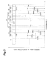
- Fig. 3 is a drawing showing energy levels of conduction bands in the cladding regions.
- the nitride semiconductor light emitting device 11 can have at least either one of structure 1 and structure 2 below. Structure 1 and structure 2 will be described with reference to the light emitting device having the conduction band energy levels shown in Fig. 3 .
- the bandgap E25a of AlGaN cladding layer 25a is preferably not less than the bandgap E26a of InAlGaN cladding layer 26a.
- the lattice-relaxed AlGaN cladding layer 25a can provide the large bandgap E25a that does not achieve with the quaternary InAlGaN cladding layer 26a.
- the thickness D26a of the InAlGaN cladding layer 26a is preferably smaller than the thickness D25a of the AlGaN cladding layer 25a. This allows use of optical confinement performance that the AlGaN cladding layer provides. In addition, it is feasible to avoid reduction in throughput due to growth of thick InAlGaN.
- the thickness D26a of the InAlGaN cladding layer 26a is preferably not less than 0.05 ⁇ m.
- the interface between the InAlGaN cladding layer and the AlGaN cladding layer (corresponding to the interface 27b in Fig. 3 ) cannot be located apart from the core semiconductor region 15 and this will result in an optical loss at this interface.
- the thickness D26a of the InAlGaN cladding layer 26a is preferably not more than 0.3 ⁇ m. Too thick InAlGaN will degrade contribution of the AlGaN cladding layer to optical confinement performance.
- the bandgap E35a of AlGaN cladding layer 35a is preferably not less than the bandgap E36a of InAlGaN cladding layer 36a.
- the lattice-relaxed AlGaN cladding layer 35a can provide the large bandgap E35a which is hard to achieve with the quaternary InAlGaN cladding layer 36a.
- the thickness D36a of the InAlGaN cladding layer 36a is preferably smaller than the thickness D35a of the AlGaN cladding layer 35a. This allows use of optical confinement performance that the AlGaN cladding layer 35a provides. Furthermore, it is feasible to avoid reduction in throughput due to growth of thick InAlGaN.
- the thickness D36a of the InAlGaN cladding layer 36a is preferably not less than 0.05 ⁇ m. If the InAlGaN cladding layer is made too thin, the interface between the InAlGaN cladding layer and the AlGaN cladding layer (corresponding to the interface 27d in Fig. 3 ) cannot be located apart from the core semiconductor region 15 and this will result in an optical loss at this interface.
- the thickness D36a of the InAlGaN cladding layer 36a is preferably not more than 0.3 ⁇ m. Too thick InAlGaN will degrade contribution of the AlGaN cladding layer to optical confinement performance.
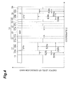
- Fig. 4 is a drawing showing energy levels of conduction bands in the cladding regions.
- the nitride semiconductor light emitting device 1 may employ at least either one of structure 3 and structure 4 below. Structure 3 and structure 4 will be described with reference to the light emitting device having the conduction band energy levels shown in Fig. 4 .
- the bandgap E26b of InAlGaN cladding layer 26b is preferably not less than the bandgap E25b of AlGaN cladding layer 25b.
- InAlGaN can be grown thick to achieve desired optical confinement performance as a whole of the cladding region 17.
- the thickness D26b of the InAlGaN cladding layer 26b is preferably larger than the thickness D25b of the AlGaN cladding layer 25b.
- the interface 27b between the InAlGaN cladding layer 26b and the AlGaN cladding layer 25b can be located apart from the core semiconductor region 15.
- the thickness D26b of the InAlGaN cladding layer 26b is preferably not less than 0.05 ⁇ m. If the InAlGaN layer is made too thin, the interface between the InAlGaN cladding layer and the AlGaN cladding layer cannot be located apart from the core semiconductor region and this will result in an optical loss from scattering at this interface (corresponding to the interface 27b in Fig. 4 ). Furthermore, the thickness D26b of the InAlGaN cladding layer 26b is preferably not more than 1.0 ⁇ m. The maximum thickness of 1.0 ⁇ m is practical even in the case of InAlGaN which does not allow a large growth rate.
- the bandgap E36b of InAlGaN cladding layer 36b is preferably not less than the bandgap E25b of AlGaN cladding layer 35b.
- thick InAlGaN can be grown in thickness to achieve desired optical confinement performance as a whole of the cladding region 19.
- the thickness D36b of the InAlGaN cladding layer 36b is preferably larger than the thickness D35b of the AlGaN cladding layer 35b.
- the interface 27d between the InAlGaN cladding layer 36b and the AlGaN cladding layer 35b can be located apart from the core semiconductor region 15.
- the thickness D36b of the InAlGaN cladding layer 36b is preferably not less than 0.05 ⁇ m. If the InAlGaN layer is too thin, the interface between the InAlGaN cladding layer and the AlGaN cladding layer cannot be located apart from the core semiconductor region and this will result in an optical loss from scattering at this interface (corresponding to the interface 27d in Fig. 4 ).
- the thickness D36b of the InAlGaN cladding layer 36b is preferably not more than 1.0 ⁇ m. The maximum thickness of 1.0 ⁇ m is practical even in the case of InAlGaN which does not allow a large growth rate.
- a light emitting device can be constructed in a combination of structure 1 and structure 4.
- Another light emitting device can be constructed in a combination of structure 2 and structure 3. In these light emitting devices, technical contribution is achieved according to the combination of structures.
- This nitride laser diode has an LD structure shown in Fig. 7 (a) .
- Step S101 is carried out to prepare a GaN substrate 51 having a semipolar plane.
- a primary surface 51a of this GaN substrate 51 is inclined at 75 degrees to the m-axis direction.
- the laser diode (LD) structure to emit light in the 450 nm band was produced on a (20-21) plane of this semipolar GaN substrate.
- a normal vector NV and a c-axis vector VC are shown along with a normal axis Nx and the c-axis Cx of the primary surface 51a.
- plural gallium nitride based semiconductor layers are grown on the GaN substrate 51 by organometallic vapor phase epitaxy to produce an epitaxial substrate.
- Raw materials used are as follows: trimethyl gallium (TMG), trimethyl aluminum (TMA); trimethyl indium (TMI); and ammonia (NH 3 ).
- Dopant gases used are as follows: silane (SiH 4 ); and bis(cyelopentadienyl) magnesium (Cp 2 Mg).
- Step S102 is carried out to place the GaN substrate 51 in a growth reactor 10.
- Thermal cleaning of the GaN substrate 51 is carried out using the growth reactor 10.
- a thermal treatment for ten minutes is carried out at the temperature of 1050 degrees Celsius under flow of gas containing NH 3 and H 2 in the growth reactor 10.
- raw material gases are supplied to the growth reactor 10 to grow an n-type Al 0.06 Ga 0.94 N cladding layer (1.9 ⁇ m thick) 53a on the primary surface 51a of the GaN substrate 51, at 1100 degrees Celsius.
- the presence/absence of lattice relaxation on the semipolar plane can be controlled by the composition, thickness, and lattice constant difference of the grown AlGaN semiconductor and in the present example, the AlGaN semiconductor is relaxed.
- step S103 is carried out to change the growth temperature to 840 degrees Celsius and then grow an n-type In 0.02 Al 0.09 Ga 0.89 N cladding layer (100 nm thick) 55 on the cladding layer 53a. After this growth, the core semiconductor region is grown thereon. The growth temperature is changed to 1100 degrees Celsius and thereafter an n-type GaN optical guide layer (100 nm thick) 57a is grown on the cladding layers 53a, 55. Then an undoped In 0.02 Ga 0.98 N optical guide layer (50 nm thick) 57b is grown thereon at the temperature of 840 degrees Celsius. An active layer 59 of a quantum well structure is grown on the optical guide layer 57b.
- the active layer 59 includes well layers and barrier layers which are alternately arranged and the number of well layers is three.
- the growth temperature of the InGaN well layers is 790 degrees Celsius and the thickness thereof is 3 nm.
- the growth temperature of the GaN barrier layers is 840 degrees Celsius and the thickness thereof is 15 nm.
- an undoped In 0.02 Ga 0.98 N optical guide layer (50 nm thick) 61a is subsequently grown thereon at the same temperature. Then, at the temperature of 1000 degrees Celsius, a p-type GaN optical guide layer (50 nm thick) 61b is grown on the optical guide layer 61a.
- a p-type Al 0.12 Ga 0.88 N electron block layer (20 nm thick) 63 is grown on the optical guide layer 61b.
- a p-type GaN optical guide layer (100 nm thick) 61c is grown on the electron block layer 63.
- the growth temperature is changed to 840 degrees Celsius and a p-type In 0.02 Al 0.09 Ga 0.89 N cladding layer (100 nm thick) 65 is grown thereon.
- a semiconductor laminate 53b is formed through these steps.
- step S104 is carried out to grow a p-type Al 0.06 Ga 0.94 N cladding layer (400 nm thick) 67 and a p-type GaN contact layer (50 nm thick) 69 on the cladding layer 65, at the temperature of 1000 degrees Celsius in the growth reactor 10.
- This step results in forming a p-type semiconductor laminate 53c.
- the above process produces an epitaxial substrate E2.
- the bandgap energy of Al 0.06 Ga 0.94 N is 3.57 eV and the bandgap energy of In 0.02 Al 0.09 Ga 0.89 N is 3.54 eV.
- the lattice constant of In 0.02 Al 0.09 Ga 0.89 N is virtually lattice-matched with GaN.
- misfit dislocations is carried out with a transmission electron microscope image.
- the misfit dislocation density at a junction interface 49a between the AlGaN cladding layer 53a and the InAlGaN cladding layer 55 is 8 ⁇ 10 4 cm -1 .
- the misfit dislocation density at a junction interface 49b between the AlGaN cladding layer 67 and the InAlGaN cladding layer 65 is 8 ⁇ 10 4 cm -1 .
- an LD structure is produced, and the LD structure has an n-side cladding layer consisting of an Al 0.06 Ga 0.94 N single layer in the thickness of 2 ⁇ m and a p-side cladding layer consisting of Al 0.06 Ga 0.94 N in the thickness of 400 nm.
- the n-side cladding layer is made of Al 0.06 Ga 0.94 N grown at 1100 degrees Celsius.
- an n-type GaN optical guide layer (100 nm thick) 67a an undoped In 0.02 Ga 0.98 N optical guide layer (50 nm thick) 67b, an active layer 69 of the quantum well structure, an undoped In 0.02 Ga 0.98 N optical guide layer (50 nm thick) 71a, a p-type GaN optical guide layer (50 nm thick) 71b, a p-type Al 0.12 Ga 0.88 N electron block layer (20 nm thick) 73, and a p-type GaN optical guide layer (100 nm thick) 71c.
- a p-side cladding layer 77 and a p-type GaN contact layer (50 nm thick) 79 are grown thereon. This process produces an epitaxial substrate EC.
- the epitaxial substrate EC is different in junctions where misfit dislocations are generated, from the epitaxial substrate E2.
- many misfit dislocations are observed at an interface 49e between the n-side cladding layer 63a and the n-type GaN optical guide layer 67a and at an interface 49f between the p-side cladding layer 77 and the p-type optical guide layer 71c.
- the misfit dislocation density at the interface 49e is 8 ⁇ 10 4 cm -1 and the misfit dislocation density at the interface 49f 4 ⁇ 10 4 cm -1 .
- An electrode step is carried out to form a p-side electrode 70a of Ni/Au in a stripe window of silicon oxide film (10 ⁇ m wide) and to form a pad electrode of Ti/Au on the epitaxial substrates E2 and EC.
- An n-side electrode 70b of Ti/Al and a pad electrode of Ti/Au are formed on the back surface of the GaN substrate 51. These electrodes are formed by vapor deposition.
- substrate products P2, PC are fabricated from the epitaxial substrates E2 and EC.
- the substrate products P2, PC are cleaved at intervals of 800 ⁇ m to produce respective gain-guiding type laser diodes LD2, LC1.
- a dielectric multilayer film of SiO 2 /TiO 2 is formed on cleaved facets.
- Threshold currents of the laser diodes LD2, LC1 are 750 mA and 900 mA, respectively. Intensities of spontaneous emissions in the laser diodes LD2, LC1 are compared with each other and they are nearly equal to each other. Since in the laser diode LD2 the waveguide loss is reduced because of the separation of the dislocation interfaces from the waveguide region, it is considered that the laser diode LD2 of the example demonstrated the lower threshold than the laser diode LC 1 of the comparative example.
- a nitride laser diode LD3 of Example 2 has an LD structure shown in Fig. 8 (a) .
- the laser diode LD3 is different in structures of the n-side cladding and p-side cladding from the laser diode LD2.
- the laser diode LD3 has an n-side cladding layer of an n-type Al 0.04 Ga 0 . 96 N cladding layer (1.6 ⁇ m thick) 81a and an n-type In 0.02 Al 0.09 Ga 0.89 N cladding layer (400 nm thick) 81b.
- the laser diode LD3 has a p-side cladding layer consisting of a p-type In 0.02 Al 0.09 Ga 0.89 N cladding layer (400 nm thick) 83.
- the Al composition of the n-type AlGaN cladding layer is reduced from 0.06 to 0.04 and the thickness of the n-type AlGaN cladding layer is reduced from 1.9 ⁇ m to 1.6 ⁇ m.
- the thickness of the n-type InAlGaN cladding layer is increased from 100 nm to 400 nm.
- the bandgap energy of Al 0.04 Ga 0.96 N is 3.52 eV and the bandgap energy of In 0.02 Al 0.09 Ga 0.89 N is 3.54 eV.
- a nitride laser diode LC2 of a comparative example has an LD structure shown in Fig. 8 (b) .
- the laser diode LC2 is different in the structure of the n-side cladding from the laser diode LD3.
- the laser diode LC2 has an n-side cladding layer consisting of a single n-type In 0.02 Al 0.09 Ga 0.89 N cladding layer (2 ⁇ m thick) 85.
- misfit dislocations are observed at an interface between the AlGaN layer 81a and the AlGaN layer 81b.
- the misfit dislocation density was 2 ⁇ 10 4 cm -1 .
- the cladding layer of the laser diode LC2 is made of InAlGaN, there are no misfit dislocations observed at a junction associated with the cladding layer.
- Thresholds of the laser diode LD3 and the laser diode LC2 are approximately 800 mA. Although misfit dislocations are introduced to the laser diode LD3, the threshold of the laser diode LD3 is nearly equal to the threshold of the laser diode LC2 without misfit dislocations. This shows that the misfit dislocations in the cladding region in the laser diode LD3 cause no significant effect on waveguide of light in the laser stripe.
- the epitaxial growth for the epitaxial substrate in the laser diode LD3 is approximately 2.5 hours, whereas the epitaxial growth for the epitaxial substrate in the laser diode LC2 is approximately 3.7 hours. This is because the growth of InAlGaN requires a long period of time.
- the laser diode LD3 adopts the multilayer cladding of AlGaN and InAlGaN. This shows that the laser diode LD3 can achieve an improvement in throughput, without deterioration of laser properties, by employment of the two-layer cladding.
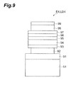
- a substrate prepared is a GaN substrate 51 having a primary surface with a 75 degree off angle.
- the following gallium nitride based semiconductor films are grown on this GaN substrate 51: n-type GaN buffer layer 91; n-type Al 0.08 Ga 0.92 N cladding layer (1.2 ⁇ m thick) 92; n-type GaN optical guide layer (300 nm thick) 93; InGaN/GaN active layer (well layers 3 nm thick and barrier layers 15 nm thick) 94; undoped GaN optical guide layer (50 nm thick) 95; p-type Al 0.11 Ga 0.89 N electron block layer (10 nm thick) 96; p-type GaN optical guide layer (250 nm thick) 97; p-type Al 0.08 Ga 0.92 N cladding layer (400 nm thick) 98; and p-type GaN contact layer (50 nm thick) 99.
- Fig. 10 is a drawing showing reciprocal lattice mapping of (20-24) in the epitaxial substrate.
- a direction of incidence of X-ray is a direction parallel to the direction of inclination of the c-axis.
- a diffraction spot S CLAD of the AlGaN cladding layer is shifted from a diffraction spot S SUB of the GaN substrate, and the n-type AlGaN cladding layer is lattice-relaxed.
- a diffraction spot of the p-type AlGaN cladding layer is approximately superimposed on the diffraction spot of the n-type AlGaN cladding layer.
- the p-type AlGaN cladding layer is lattice-relaxed.
- a diffraction spot S GUIDE of the GaN optical guide layers is shifted from the diffraction spot S SUB of the GaN substrate.
- the GaN optical guide layers are lattice-relaxed.
- the diffraction spot S GUIDE of the GaN optical guide layers is shifted toward the diffraction spot S SUB of the GaN substrate from the diffraction spots S CLAD of the AlGaN claddings, the core semiconductor region having the GaN optical guide layers and the light emitting layer is relaxed on the AlGaN cladding layer, and the lattice constants of the core semiconductor region are freed from constraints of the AlGaN cladding.
- the laser structure LD4 includes lattice relaxations at three locations. Namely, since the plural diffraction spots are not aligned on a straight line parallel to the y-axis, these three semiconductors are not in a lattice-matched state.
- the embodiments are directed to the purpose to provide the nitride semiconductor light emitting device capable of improving the optical confinement performance and reducing the optical loss due to dislocations in the light emitting device formed on the nonpolar plane.
Landscapes
- Physics & Mathematics (AREA)
- Optics & Photonics (AREA)
- Condensed Matter Physics & Semiconductors (AREA)
- General Physics & Mathematics (AREA)
- Electromagnetism (AREA)
- Engineering & Computer Science (AREA)
- Nanotechnology (AREA)
- Chemical & Material Sciences (AREA)
- Biophysics (AREA)
- Crystallography & Structural Chemistry (AREA)
- Life Sciences & Earth Sciences (AREA)
- Led Devices (AREA)
- Semiconductor Lasers (AREA)
Abstract
A nitride semiconductor light emitting device is provided as one capable of improving optical confinement performance and reducing an optical loss due to dislocations in the light emitting device formed on a primary surface which is not the polar plane. A core semiconductor region 15, a first cladding region 17, and a second cladding region 19 are mounted on a nonpolar primary surface 13a of a support substrate 13 of GaN which is not the polar plane. The core semiconductor region 15 includes an active layer 21 and a carrier block layer 23. The first cladding region 17 includes an n-type AlGaN cladding layer 25 and an n-type InAlGaN cladding layer 26. The n-type InAlGaN cladding layer 26 is provided between the n-type AlGaN cladding layer 25 and the active layer 21. A misfit dislocation density at an interface 27b is larger than that at an interface 27a. The AlGaN cladding layer 25 is lattice-relaxed with respect to the GaN support substrate 13 and the InAlGaN cladding layer 26 is lattice-relaxed with respect to the AlGaN cladding layer 25.
Description
- The present invention relates to a nitride semiconductor light emitting device.
-
Patent Literature 1 describes an ultraviolet light emitting device. The ultraviolet light emitting device emits light with high efficiency at room temperature in the ultraviolet short-wavelength region of not more than the wavelength of 360 nm. This ultraviolet light emitting device has a quantum well structure, provided on a SiC substrate, including In0.37Al0.02Ga0.61N layers and In0.16Al0.06Ga0.78N layers making alternate junctions. This quantum well structure is formed directly on an Al0.40Ga0.60N layer. -
- Patent Literature 1: Japanese Patent Application Laid-open No.
2001-237455 - In
Patent Literature 1, an InAlGaN layer serves as a buffer layer and has the same composition as the barrier layers. This InAlGaN buffer layer is grown thick so as to provide the barrier layer with an extension. Furthermore, the InAlGaN layer has the same composition as the InAlGaN barrier layers formed between the well layers in the quantum well structure and in this point of view, the InAlGaN layer is different from cladding layers. - According to Inventors' knowledge, a slip plane (e.g., c-plane slip plane) becomes active on a semipolar gallium nitride (GaN) substrate and, therefore, an adjacent semiconductor layer with great strain undergoes lattice relaxation to release internal strain. For this reason, AlGaN can be grown in a higher Al composition on the semipolar GaN substrate than on a c-plane GaN substrate. Formed in this AlGaN are not cracks but misfit dislocations, thereby releasing the internal strain. When AlGaN in the high Al composition is applied to the cladding layers, a core semiconductor region between p-type and n-type cladding layers may be lattice-relaxed with respect to the cladding layers. When the difference between the lattice constant of the core semiconductor region and the lattice constant(s) of the cladding layers is large because of the high Al composition, misfit dislocations are formed at the interfaces between the cladding layers and the core semiconductor region.
- The cladding layers are provided for optical confinement, and in the cladding layers, the amplitude of light is small. When misfit dislocations due to the difference between the lattice constant of the core semiconductor region and the lattice constant(s) of the cladding layers are formed at the interfaces therebetween, the misfit dislocations cause an optical loss due to scattering of light.
- It is an object of the present invention to provide a nitride semiconductor light emitting device capable of improving the optical confinement performance and reducing the optical loss due to dislocations in the light emitting device formed on a plane which is not polar.
- A nitride semiconductor light emitting device according to one aspect of the present invention comprises: (a) a support substrate comprising a hexagonal gallium nitride semiconductor; (b) a first cladding region comprising a first conductivity type gallium nitride based semiconductor; (c) a second cladding region comprising a second conductivity type gallium nitride-based semiconductor; and (d) a core semiconductor region comprising an active layer and a carrier block layer. The c-axis of the hexagonal gallium nitride semiconductor is directed along a direction different from a normal axis to the primary surface of the support substrate, and a plane defined by the c-axis of the hexagonal gallium nitride semiconductor and the normal axis to the support substrate extends along a predetermined direction; the core semiconductor region is provided between the first cladding region and the second cladding region; the core semiconductor region, the first cladding region, and the second cladding region are mounted on the primary surface of the support substrate; the first cladding region comprises an AlGaN cladding layer and an InAlGaN cladding layer; the InAlGaN cladding layer is provided between the AlGaN cladding layer and the active layer; and the InAlGaN cladding layer makes a junction with the core semiconductor region.
- In this nitride semiconductor light emitting device, since the InAlGaN cladding layer is provided between the AlGaN cladding layer and the core semiconductor region, it becomes feasible to increase the Al composition and/or to increase the thickness of the AlGaN layer in order to enhance the optical confinement performance of the AlGaN layer. Furthermore, since quaternary InAlGaN is applied to the cladding layer, the cladding region having the AlGaN cladding layer and the InAlGaN cladding layer can provide both an excellent junction with the core semiconductor region and a lattice constant enabling to provide the refractive index necessary for the cladding layer.
- In the nitride semiconductor light emitting device according to the present invention, the first cladding region includes an interface between the AlGaN cladding layer and the InAlGaN cladding layer, and a misfit dislocation density at the interface between the InAlGaN cladding layer and the AlGaN cladding layer is larger than a misfit dislocation density at an interface between the core semiconductor region and the first cladding region.
- In this nitride semiconductor light emitting device, the misfit dislocation density at the interface between the InAlGaN cladding layer and the AlGaN cladding layer is larger than the misfit dislocation density at the interface between the core semiconductor region and the first cladding region. This allows an increase in the Al composition of the AlGaN layer and/or an increase in the thickness of the InAlGaN layer enough to induce lattice relaxation of the InAlGaN cladding layer by introduction of the misfit dislocations, thereby improving the optical confinement performance as a whole of the first cladding layer. In this structure, the interface between the core semiconductor region and the first cladding region is isolated from the interface of the larger misfit dislocation density by the InAlGaN layer.
- In the nitride semiconductor light emitting device according to the present invention, preferably, in the first cladding region, the misfit dislocation density at the interface between the InAlGaN cladding layer and the AlGaN cladding layer is not less than 1×104 cm-1. This nitride semiconductor light emitting device enables lattice relaxation to occur in one of the semiconductor layers associated with the interface when dislocations in this dislocation density are introduced to the foregoing interface. The AlGaN cladding layer in the Al composition and thickness which are enough to cause lattice relaxation can improve the optical confinement performance.
- In the nitride semiconductor light emitting device according to the present invention, it is preferable that the misfit dislocation density at the interface between the core semiconductor region and the first cladding region be less than 1×104 cm-1. This nitride semiconductor light emitting device can reduce the optical loss due to scattering of light by misfit dislocations. The core semiconductor region having a lamination of relatively thin semiconductor layers is composed of semiconductor layers coherently grown.
- In the nitride semiconductor light emitting device according to the present invention, preferably, in the first cladding region, an Al composition of the AlGaN cladding layer is not less than 0.05. The Al composition of the AlGaN cladding layer is preferably not more than 0.2.
- When the Al composition is not less than 0.05, the AlGaN cladding layer can be relaxed with respect to the InAlGaN cladding layer. A too large Al composition raises possibilities of degradation of crystal quality of the AlGaN cladding layer and relaxation of the AlGaN cladding layer in a direction perpendicular to the c-axis off direction.
- In the nitride semiconductor light emitting device according to the present invention, preferably, in the first cladding region, a thickness of the InAlGaN cladding layer is smaller than a thickness of the AlGaN cladding layer. This nitride semiconductor light emitting device can make use of the optical confinement performance of the AlGaN cladding layer, and it is also feasible to avoid reduction in throughput due to growth of thick InAlGaN.
- In the nitride semiconductor light emitting device according to the present invention, preferably, in the first cladding region, a bandgap of the InAlGaN cladding layer is not more than a bandgap of the AlGaN cladding layer. This nitride semiconductor light emitting device enables the lattice-relaxed AlGaN cladding layer to provide a large bandgap which cannot be practically employed with the quaternary InAlGaN cladding layer.
- In the nitride semiconductor light emitting device according to the present invention, preferably, in the first cladding region, the thickness of the InAlGaN cladding layer is not less than 0.05 µm. If the InAlGaN cladding layer is too thin in the nitride semiconductor light emitting device, the interface between the InAlGaN cladding layer and the AlGaN cladding layer cannot be located apart from the core semiconductor region and then an optical loss will occur at this interface. Furthermore, preferably, the thickness of the InAlGaN cladding layer is not more than 0.3 µm. In this nitride semiconductor light emitting device, too thick InAlGaN reduces contribution of the AlGaN cladding layer to the optical confinement performance.
- In the nitride semiconductor light emitting device according to the present invention, preferably, in the first cladding region, the bandgap of the InAlGaN cladding layer is not less than the bandgap of the AlGaN cladding layer.
- This nitride semiconductor light emitting device can achieve desired optical confinement performance as a whole of the cladding region even if thick InAlGaN is grown thereon such that the interface between the InAlGaN cladding layer and the AlGaN cladding layer is located apart from the core semiconductor region.
- In the nitride semiconductor light emitting device according to the present invention, preferably, in the first cladding region, the thickness of the InAlGaN cladding layer is not less than 0.05 µm. If the InAlGaN layer is too thin in this nitride semiconductor light emitting device, the interface between the InAlGaN cladding layer and the AlGaN cladding layer cannot be located apart from the core semiconductor region and then an optical loss will occur at this interface. In the nitride semiconductor light emitting device according to the present invention, preferably, the thickness of the InAlGaN cladding layer is not more than 1.0 µm. In this nitride semiconductor light emitting device, the maximum thickness of 1.0 µm is practical even in the case of InAlGaN not permitting a large growth rate.
- In the nitride semiconductor light emitting device according to the present invention, preferably, the core semiconductor region comprises a first optical guide layer; the first optical guide layer makes a junction with the InAlGaN cladding layer of the first cladding region; a lattice constant inherent to InAlGaN in the InAlGaN cladding layer of the first cladding region is not more than a lattice constant inherent to a gallium nitride based semiconductor of the first optical guide layer of the core semiconductor region; the lattice constant of the InAlGaN cladding layer of the first cladding region is larger than a lattice constant of the AlGaN cladding layer of the first cladding region.
- In this nitride semiconductor light emitting device, the lattice constant of the InAlGaN cladding layer is larger than the lattice constant of the AlGaN cladding layer and is not more than the lattice constant inherent to the first optical guide layer. When dislocations are introduced to the interface between the AlGaN cladding layer and the InAlGaN cladding layer, it is feasible to avoid generation of an optical loss from dislocations at the junction between the first optical guide layer and the InAlGaN cladding layer.
- In the nitride semiconductor light emitting device according to the present invention, preferably, the InAlGaN cladding layer is lattice-matched with the first optical guide layer with respect to a direction of projection of the c-axis onto the primary surface. In this nitride semiconductor light emitting device, the first optical guide layer is coherently grown on the InAlGaN cladding layer. The core semiconductor region is coherently grown on the InAlGaN cladding layer.
- In the nitride semiconductor light emitting device according to the present invention, preferably, the first cladding region has n-type conductivity; and a misfit dislocation density at an interface between the support substrate and the AlGaN cladding layer of the first cladding region is larger than the misfit dislocation density at the interface between the core semiconductor region and the first cladding region.
- This nitride semiconductor light emitting device can improve the optical confinement performance in the n-side semiconductor region. The AlGaN cladding layer of the first cladding region is lattice-relaxed on the support substrate. Hence, the optical confinement performance of the first cladding region can be improved by increase in the Al composition of the AlGaN cladding layer and/or increase in the thickness of the AlGaN cladding layer.
- In the nitride semiconductor light emitting device according to the present invention, preferably, the misfit dislocation density at the interface between and support substrate and the AlGaN cladding layer of the first cladding region is not less than 1×104 cm-1. In this nitride semiconductor light emitting device, the AlGaN cladding corresponding to this dislocation density can achieve excellent optical confinement.
- In the nitride semiconductor light emitting device according to the present invention, the following configuration can be adopted: the first cladding region has p-type conductivity; the nitride semiconductor light emitting device further comprises a p-type contact layer provided on the first cladding region; the core semiconductor region comprises a second optical guide layer and an electron block layer; the second optical guide layer is provided between the electron block layer and the first cladding region; the electron block layer is provided between the second optical guide layer and the active layer.
- This nitride semiconductor light emitting device can improve the optical confinement performance in the p-side semiconductor region. The p-type contact layer is provided on the lattice-relaxed AlGaN cladding layer and the lattice relaxation of the AlGaN cladding layer does not affect the p-type contact layer.
- In the nitride semiconductor light emitting device according to the present invention, preferably, the first cladding region has n-type conductivity; the second cladding region has p-type conductivity; the second cladding region comprises an AlGaN cladding layer and an InAlGaN cladding layer; the InAlGaN cladding layer of the second cladding region is provided between the active layer and the AlGaN cladding layer of the second cladding region; the InAlGaN cladding layer of the second cladding region makes a junction with the core semiconductor region; a lattice constant of the InAlGaN cladding layer of the second cladding region is larger than a lattice constant of the AlGaN cladding layer of the second cladding region.
- This nitride semiconductor light emitting device can improve the optical confinement performance in the p-side semiconductor region and in the n-side semiconductor region.
- In the nitride semiconductor light emitting device according to the present invention, preferably, a misfit dislocation density at an interface between the AlGaN cladding layer and the InAlGaN cladding layer of the second cladding region is larger than a misfit dislocation density at an interface between the core semiconductor region and the second cladding region.
- In this nitride semiconductor light emitting device, the p-type AlGaN layer and the n-type InAlGaN layer in the p-side semiconductor region and in the n-side semiconductor region, respectively, are lattice-relaxed.
- In the nitride semiconductor light emitting device according to the present invention, the misfit dislocation density at the interface between the AlGaN cladding layer and the InAlGaN cladding layer of the second cladding region can be not less than 1×104 cm-1.
- This nitride semiconductor light emitting device enables lattice relaxation to occur in one of the semiconductor layers associated with the interface when dislocations in this dislocation density are introduced to the foregoing interface. This lattice relaxation can achieve excellent optical confinement by the AlGaN cladding layer.
- In the nitride semiconductor light emitting device according to the present invention, preferably, an angle between the c-axis of the hexagonal gallium nitride semiconductor and the normal axis to the support substrate is not less than 10 degrees. Furthermore, the angle is preferably not more than 170 degrees. This nitride semiconductor light emitting device can achieve excellent optical confinement performance by making use of generation of a slip plane in a polarity which is not polar (polarity of semipolar nature and polarity of nonpolar nature).
- In the nitride semiconductor light emitting device according to the present invention, preferably, the angle is in the range of not less than 10 degrees and not more than 80 degrees or in the range of not less than 100 degrees and not more than 170 degrees. This nitride semiconductor light emitting device can achieve excellent optical confinement performance by making use of generation of a slip plane in semipolar nature.
- In the nitride semiconductor light emitting device according to the present invention, preferably, the angle is in the range of not less than 63 degrees and not more than 80 degrees or in the range of not less than 100 degrees and not more than 117 degrees.
- In this nitride semiconductor light emitting device, it is easy to generate dislocations by introduction of a slip plane, device design flexibility is made high in this angular range. A semipolar plane in this angular range tends to provide an excellent In incorporation.
- The above object and other objects, features, and advantages of the present invention will more readily become apparent in view of the following detailed description of the preferred embodiments of the present invention proceeding with reference to the accompanying drawings.
- As described above, the object of the present invention is to provide the nitride semiconductor light emitting device capable of improving the optical confinement performance and reducing the optical loss due to dislocations in the light emitting device formed on the nonpolar plane.
-
-
Fig. 1 is a drawing schematically showing a nitride semiconductor light emitting device according to an embodiment of the present invention. -
Fig. 2 is a drawing showing a relationship between semiconductor layers and lattice constants thereof, and the semiconductor layers constitutes an epitaxial substrate E1 for the nitride semiconductor light emitting device shown inFig. 1 . -
Fig. 3 is a drawing showing energy levels of conduction bands in cladding regions. -
Fig. 4 is a drawing showing energy levels of conduction bands in cladding regions. -
Fig. 5 is a drawing showing major steps in a method for fabricating a nitride laser diode. -
Fig. 6 is a drawing showing major steps in the method for fabricating the nitride laser diode. -
Fig. 7 is a drawing showing structures of nitride laser diodes in an example and a comparative example. -
Fig. 8 is a drawing showing structures of nitride laser diodes in an example and a comparative example. -
Fig. 9 is a drawing showing an epitaxial substrate for measurement of reciprocal lattice mapping. -
Fig. 10 is a drawing showing a reciprocal lattice mapping image of (20-24) in the epitaxial substrate. - The expertise of the present invention can be readily understood in view of the following detailed description with reference to the accompanying drawings presented by way of illustration. The following will describe embodiments of the nitride semiconductor light emitting device and epitaxial substrate of the present invention, with reference to the accompanying drawings. The same portions will be denoted by the same reference signs as much as possible.
-
Fig. 1 is a drawing schematically showing the nitride semiconductor light emitting device according to an embodiment of the present invention.Fig. 2 is a drawing showing the relationship between semiconductor layers, which form an epitaxial substrate E1 of the nitride semiconductor light emitting device shown inFig. 1 , and lattice constants thereof. - The nitride semiconductor
light emitting device 11 has asupport substrate 13, acore semiconductor region 15, afirst cladding region 17, and asecond cladding region 19. With reference toFig. 1 , there are an orthogonal coordinate system S, a c-axis vector VC, and a normal vector NV shown. Thesupport substrate 13 is comprised of a hexagonal gallium nitride (GaN) semiconductor. The c-axis (indicated by a vector VC) Cx of this hexagonal GaN semiconductor is inclined toward a predetermined direction (e.g., the X-axis direction) with respect to a normal axis Nx to aprimary surface 13a of thesupport substrate 13. The predetermined direction can be the a-axis, the m-axis, or the like of the hexagonal GaN semiconductor. Theprimary surface 13a can have nonpolar (semipolar or nonpolar) nature and is parallel to a plane defined by the X-axis and Y-axis. The c-axis Cx of the hexagonal GaN semiconductor is directed along a direction different from the normal axis Nx to theprimary surface 13a of thesupport substrate 13. A plane defined by the normal axis Nx and the c-axis Cx of thesupport substrate 13 extends along the predetermined direction. Thefirst cladding region 17 comprises a first conductivity type (e.g., n-type) GaN-based semiconductor. Thesecond cladding region 19 comprises a second conductivity type (e.g., p-type) GaN-based semiconductor. Thecore semiconductor region 15 includes anactive layer 21 and acarrier block layer 23. Thecore semiconductor region 15 is provided between thefirst cladding region 17 and thesecond cladding region 19. Thecore semiconductor region 15, thefirst cladding region 17, and thesecond cladding region 19 are mounted on theprimary surface 13a of thesupport substrate 13. - In
Fig. 1 both of thefirst cladding region 17 and thesecond cladding region 19 have a cladding structure which have two layers, but either one of thefirst cladding region 17 and thesecond cladding region 19 can have the cladding structure mentioned above. - In an embodiment, the
first cladding region 17 includes an n-typeAlGaN cladding layer 25 and an n-typeInAlGaN cladding layer 26. The n-typeInAlGaN cladding layer 26 is provided between the n-typeAlGaN cladding layer 25 and theactive layer 21. The n-typeInAlGaN cladding layer 26 makes ajunction 27a with thecore semiconductor region 15. - Since this nitride semiconductor
light emitting device 11 has theInAlGaN cladding layer 26 provided between theAlGaN cladding layer 25 and thecore semiconductor region 15, it becomes feasible to increase the Al composition and/or to increase the thickness of theAlGaN layer 25 in order to enhance the optical confinement performance of theAlGaN layer 25. In addition, since quaternary InAlGaN is applied to the cladding layer, thecladding region 17 that has theAlGaN cladding layer 25 and theInAlGaN cladding layer 26 can provide both the refractive index necessary for the cladding and the lattice constant to make theexcellent junction 27a with thecore semiconductor region 15. - The
first cladding region 17 includes aninterface 27b between theAlGaN cladding layer 25 and theInAlGaN cladding layer 26. The misfit dislocation density at theinterface 27b between theInAlGaN cladding layer 26 and theAlGaN cladding layer 25 is larger than that at theinterface 27a between thecore semiconductor region 15 and thefirst cladding region 17. This is based on the following: the more theInAlGaN cladding layer 26 is lattice-relaxed by introduction of the misfit dislocation density, the more the increase in the Al composition and/or the thickness of theAlGaN layer 25 can be made, thereby permitting improvement in the optical confinement performance as a whole of thefirst cladding region 17. In this structure, theinterface 27a between thecore semiconductor region 15 and thefirst cladding region 17 is isolated by the InAlGaN layer from theinterface 27b that has the larger misfit dislocation density. - In the
first cladding region 17, the Al composition of theAlGaN cladding layer 25 is preferably not less than 0.05. When the Al composition is not less than 0.05, theAlGaN cladding layer 25 in a practical thickness can be relaxed on the GaN support substrate. At this time, theInAlGaN cladding layer 26 can be relaxed on theAlGaN cladding layer 25. The Al composition of theAlGaN cladding layer 25 is preferably not more than 0.2. A too large Al composition will raise possibilities of relaxation of theAlGaN cladding layer 25 in a direction perpendicular to the c-axis off direction and deterioration of crystal quality of theAlGaN cladding layer 25. - In an embodiment, the
second cladding region 19 includes a p-typeAlGaN cladding layer 35 and a p-typeInAlGaN cladding layer 36. The p-typeInAlGaN cladding layer 36 is provided between the p-typeAlGaN cladding layer 35 and theactive layer 21. The p-typeInAlGaN cladding layer 35 makes ajunction 27c with thecore semiconductor region 15. - Since this nitride semiconductor
light emitting device 11 is provided with theInAlGaN cladding layer 36 between theAlGaN cladding layer 35 and thecore semiconductor region 15, it becomes feasible to increase the Al composition and/or to increase the thickness of theAlGaN layer 35 in order to enhance the optical confinement performance of theAlGaN layer 35. In addition, since quaternary InAlGaN is applied to thecladding layer 36, thesecond cladding region 19 that has theAlGaN cladding layer 35 and theInAlGaN cladding layer 36 can provide both the refractive index necessary for the cladding and the lattice constant to make theexcellent junction 27c with thecore semiconductor region 15. - The
second cladding region 19 includes aninterface 27d between theAlGaN cladding layer 35 and theInAlGaN cladding layer 36. The misfit dislocation density at theinterface 27d between theInAlGaN cladding layer 36 and theAlGaN cladding layer 35 is larger than that at theinterface 27c between thecore semiconductor region 15 and thesecond cladding region 19. This is based on the following: the more theAlGaN cladding layer 35 is lattice-relaxed by introduction of the misfit dislocation density, the more the increase in the Al composition and/or the thickness of theAlGaN layer 35 can be made, thereby permitting improvement in the optical confinement performance as a whole of thesecond cladding region 19. In this structure, theinterface 27c between thecore semiconductor region 15 and thesecond cladding region 19 is isolated by the InAlGaN layer from theinterface 27d that has the larger misfit dislocation density. - In the
second cladding region 19, the Al composition of theAlGaN cladding layer 35 is preferably not less than 0.05. When the Al composition is not less than 0.05, theAlGaN cladding layer 35 can be relaxed on the GaN support substrate. At this time, theAlGaN cladding layer 35 can be relaxed on theInAlGaN cladding layer 36. The Al composition of theAlGaN cladding layer 35 is preferably not more than 0.2. A too large Al composition will raise possibilities of relaxation of theAlGaN cladding layer 35 in the direction perpendicular to the c-axis off direction and deterioration of crystal quality of theAlGaN cladding layer 35. - In the
first cladding region 17, the misfit dislocation density at theinterface 27b between theInAlGaN cladding layer 26 and theAlGaN cladding layer 25 is preferably not less than 1×104cm-1. When dislocations in this dislocation density are introduced to theinterface 27b, one of the semiconductor layers associated with theinterface 27b is lattice-relaxed. The lattice relaxation can provide theAlGaN cladding layer 25 suitable for optical confinement. - The misfit dislocation density at the
interface 27a between thecore semiconductor region 15 and thefirst cladding region 17 is preferably less than 1×104 cm-1. This can reduce the optical loss due to scattering of light caused by misfit dislocations. Thecore semiconductor region 15 that has a lamination of relatively thin semiconductor layers is composed of coherently grown semiconductor layers 21, 23, 29, 31, 33, and 37. - Furthermore, in the
second cladding region 19, the misfit dislocation density at theinterface 27d between theInAlGaN cladding layer 36 and theAlGaN cladding layer 35 is preferably not less than 1×104 cm-1. When dislocations in this dislocation density are introduced to theinterface 27d, one of the semiconductor layers associated with theinterface 27d is lattice-relaxed. The lattice relaxation can provide theAlGaN cladding layer 35 suitable for optical confinement. - The relation of the lattice constants in the c-axis direction will be described in more detail with reference to
Fig. 2 . This relation is also applicable similarly to the lattice constants in the a-axis and m-axis directions. A c-axis direction in AlGaN of the n-typeAlGaN cladding layer 25 and a magnitude of lattice constant d25 in the c-axis direction are represented by a lattice vector LVC25. The lattice vector LVC25 has a longitudinal component V25L in the direction of the normal axis Nx and a transverse component V25T perpendicular to the longitudinal component. A c-axis direction in InAlGaN of the n-typeInAlGaN cladding layer 26 and a magnitude of lattice constant d26 in the c-axis direction are represented by a lattice vector LVC26. The lattice vector LVC26 has a longitudinal component V26L in the direction of the normal axis Nx and a transverse component V26T perpendicular to the longitudinal component. The transverse component V25T is smaller than the transverse component V26T. - A c-axis direction in a GaN-based semiconductor of the GaN-based
semiconductor layer 31 and a magnitude of lattice constant d31 in the c-axis direction are represented by a lattice vector LVC31. The lattice vector LVC31 has a longitudinal component V31L in the direction of the normal axis Nx and a transverse component V31T perpendicular to the longitudinal component. The transverse component V25T is smaller than the transverse component V31T. - A c-axis direction in AlGaN of the p-type
AlGaN cladding layer 35 and a magnitude of lattice constant d35 in the c-axis direction are represented by a lattice vector LVC35. The lattice vector LVC35 has a longitudinal component V35L in the direction of the normal axis Nx and a transverse component V35T perpendicular to the longitudinal component. A c-axis direction in InAlGaN of the p-typeInAlGaN cladding layer 36 and a magnitude of lattice constant d36 in the c-axis direction are represented by a lattice vector LVC36. The lattice vector LVC36 has a longitudinal component V36L in the direction of the normal axis Nx and a transverse component V36T perpendicular to the longitudinal component. The transverse component V35T is smaller than the transverse component V36T. - A c-axis direction in a GaN-based semiconductor of the GaN-based
semiconductor layer 33 and a magnitude of lattice constant d33 in the c-axis direction are represented by a lattice vector LVC33. The lattice vector LVC33 has a longitudinal component V33L in the direction of the normal axis Nx and a transverse component V33T perpendicular to the longitudinal component. The transverse component V35T is smaller than the transverse component V33T. - A c-axis direction in the GaN-based semiconductor of the
support substrate 13 and a magnitude of lattice constant d13 in the c-axis direction are represented by a lattice vector LVC13. The lattice vector LVC13 has a longitudinal component V13L in the direction of the normal axis Nx and a transverse component V13T perpendicular to the longitudinal component. The transverse component V25T is smaller than the transverse component V13T. - The misfit dislocation density at an
interface 27e between theAlGaN cladding layer 25 of thefirst cladding region 17 and thesupport substrate 13 is preferably larger than that at theinterface 27a between thecore semiconductor region 15 and thefirst cladding region 17. This allows reduction in the refractive index of theAlGaN cladding layer 25 and thus permits improvement in optical confinement performance in thecore semiconductor region 15. Furthermore, theAlGaN cladding layer 25 of thefirst cladding region 17 is lattice-relaxed on thesupport substrate 13. For this reason, the optical confinement performance by thefirst cladding region 17 can be improved by increase in the Al composition of theAlGaN cladding layer 25 and/or increase in the thickness of theAlGaN cladding layer 25. - The misfit dislocation density at the
interface 27e between theAlGaN cladding layer 26 of thefirst cladding region 17 and thesupport substrate 13 is preferably not less than 1×104 cm-1. AlGaN satisfying this dislocation density can provide excellent optical confinement. - In the nitride-based
light emitting device 11, theAlGaN cladding layer 25 of the n-type cladding region 17 is lattice-relaxed on theprimary surface 13a, which is not polar, of thesupport substrate 13. The thickness D25 of theAlGaN cladding layer 25 is preferably over a critical thickness in the Al composition of theAlGaN cladding layer 25. The transverse component V13T of the lattice constant is larger than the transverse component V25T of the lattice constant of the n-typeAlGaN cladding layer 25. - The
InAlGaN cladding layer 25 of the n-type cladding region 17 is lattice-relaxed on a plane, which is not polar, of theAlGaN cladding layer 25. The thickness D26 of theInAlGaN cladding layer 26 is preferably over a critical thickness in the Al composition and In composition of theInAlGaN cladding layer 26. The transverse component V25T of the lattice constant is smaller than the transverse component V26T of the lattice constant of the n-typeInAlGaN cladding layer 26. The GaN-basedsemiconductor layer 31,active layer 21, GaN-basedsemiconductor layer 37,electron block layer 23, GaN-basedsemiconductor layer 33, andInAlGaN cladding layer 36 are coherently grown on theInAlGaN cladding layer 26. Hence, as shown inFig. 2 , the transverse components of the lattice constants of the GaN-basedsemiconductor layer 31,active layer 21, GaN-basedsemiconductor layer 37,electron block layer 23, GaN-basedsemiconductor layer 33, andInAlGaN cladding layer 36 are equal to each other. - Since the
interfaces interface 27a between thecore semiconductor region 15 and thecladding region 17, the optical loss from scattering due to dislocations is small. - In the nitride-based
light emitting device 11, theAlGaN cladding layer 35 of the p-type cladding region 19 is lattice-relaxed on a primary surface, which is not polar, of theInAlGaN cladding layer 36. The thickness D35 of theAlGaN cladding layer 35 is preferably over a critical thickness in the Al composition of theAlGaN cladding layer 35. The transverse component V35T of the lattice constant is smaller than the transverse component V36T of the lattice constant of theInAlGaN cladding layer 36. - The
InAlGaN cladding layer 36 of the p-type cladding region 19 is not lattice-relaxed on a plane of thecore semiconductor region 15. The thickness D36 of theInAlGaN cladding layer 36 is preferably not more than a critical thickness in the Al composition and In composition of theInAlGaN cladding layer 36. TheInAlGaN cladding layer 36 is coherently grown on the plane, which is not polar, of thecore semiconductor region 15 coherently grown on theInAlGaN cladding layer 26. The transverse component V36T of the lattice constant is lattice-matched with the transverse component V33T of the lattice constant of the GaN-basedsemiconductor layer 33. - Since the
interface 27d at the large dislocation density is located apart from theinterface 27c between thecore semiconductor region 15 and thecladding region 19, the optical loss from scattering due to dislocations is small. - As shown in
Figs. 1 and2 , theactive layer 21 has aquantum well structure 29. Thequantum well structure 29 includes barrier layers 29a and well layers 29b which are alternately arranged. The barrier layers 29a comprises, for example, InGaN, GaN, or the like and thewell layers 29b comprises, for example, InGaN or the like. The well layers 29b incorporates strain according to the difference between the lattice constant of the well layers 29b and the lattice constant of the GaN-basedsemiconductor layer 31, and thebarrier layers 29a incorporates strain according to the difference between the lattice constant of the barrier layers 29a and the lattice constant of the GaN-basedsemiconductor layer 31. - The first gallium nitride based
semiconductor layer 31 can serve as an optical guide layer. The second gallium nitride basedsemiconductor layer 33 can serve as an optical guide layer. The third gallium nitride basedsemiconductor layer 37 can serve as an optical guide layer. The refractive index of the first gallium nitride basedsemiconductor layer 31 is larger than that of thefirst cladding region 17. The refractive index of the second and third gallium nitride based semiconductor layers 33, 37 is larger than that of theelectron block layer 23 and larger than that of the p-type cladding layer 19. The first gallium nitride basedsemiconductor layer 31 includes first andsecond semiconductor layers first semiconductor layer 31a is larger than that of thesecond semiconductor layer 31b. The third gallium nitride basedsemiconductor layer 37 includes first andsecond semiconductor layers first semiconductor layer 37a is smaller than that of thesecond semiconductor layer 37b. - As shown in
Fig. 1 , the nitride semiconductorlight emitting device 11 can include a p-type contact layer 39 provided on the p-type cladding layer 19. The p-type contact layer 39 can comprise GaN, AlGaN, or the like. A p-side electrode 41a is in contact with the p-type contact layer 39 through an aperture of insulatingfilm 43. - The nitride semiconductor
light emitting device 11 can include an n-side electrode 41b in contact with aback surface 13b of thesupport substrate 13. An angle ALPHA between the c-axis (VC) of the hexagonal gallium nitride semiconductor of thesupport substrate 13 and the normal axis Nx is preferably not less than 10 degrees. The foregoing angle is preferably not more than 170 degrees. In this range, excellent optical confinement performance can be achieved by making use of generation of a slip plane in a nature which is not polar (semipolar and nonpolar natures). The angle ALPHA is preferably in the range of not less than 10 degrees and not more than 80 degrees or in the range of not less than 100 degrees and not more than 170 degrees. In this angular range, excellent optical confinement performance can be achieved by making use of generation of a slip plane in semipolar nature. Furthermore, the angle ALPHA is preferably in the range of not less than 63 degrees and not more than 80 degrees or in the range of not less than 100 degrees and not more than 117 degrees. In this angular range, it is easy to generate dislocations by introduction of a slip plane and degrees of freedom are high for design of device. A semipolar plane in this angular range tends to be excellent in In incorporation. - As shown in
Fig. 2 , the gallium nitride basedsemiconductor layer 31 of thecore semiconductor region 15 makes thejunction 27a with theInAlGaN cladding layer 26 of thefirst cladding region 17. The lattice constant d26 of theInAlGaN cladding layer 26 is equal to the lattice constant inherent to InAlGaN in theInAlGaN cladding layer 26 when theInAlGaN cladding layer 26 is perfectly lattice-relaxed. The lattice constant d25 of theAlGaN cladding layer 25 is equal to the lattice constant inherent to AlGaN in theAlGaN cladding layer 25 when theAlGaN cladding layer 25 is perfectly lattice-relaxed. The lattice constant d26 is not more than the lattice constant d310 (peculiar to the gallium nitride based semiconductor of the gallium nitride based semiconductor layer 31) when the gallium nitride basedsemiconductor layer 31 is unstrained. The lattice constant d26 is preferably larger than the lattice constant d25. - When the relation of the lattice constants (
d3 10 ≥ d26 > d25) is satisfied, dislocations are introduced to the interface between theAlGaN cladding layer 25 and theInAlGaN cladding layer 26, with increase in the difference between the lattice constant d26 and the lattice constant d25. At this time, the difference between the lattice constant d26 and the lattice constant d310 becomes smaller, so as to be able to avoid generation of optical loss due to dislocations at thejunction 27a between the first optical guide layer and theInAlGaN cladding layer 26. The gallium nitride basedsemiconductor layer 31 is coherently grown on theInAlGaN cladding layer 26. Thecore semiconductor region 15 is coherently grown on theInAlGaN cladding layer 26. For example, theInAlGaN cladding layer 26 is preferably lattice-matched with the gallium nitride basedsemiconductor layer 31 with respect to a direction of projection of the c-axis onto theprimary surface 13a. When the relation of the lattice constants (d330 ≥ d36 > d35) is satisfied, the same technical contribution as above is achieved. -
Fig. 3 is a drawing showing energy levels of conduction bands in the cladding regions. The nitride semiconductorlight emitting device 11 can have at least either one ofstructure 1 and structure 2 below.Structure 1 and structure 2 will be described with reference to the light emitting device having the conduction band energy levels shown inFig. 3 . -
Structure 1 will be described. With reference toFig. 3 , in thefirst cladding region 17, the bandgap E25a ofAlGaN cladding layer 25a is preferably not less than the bandgap E26a ofInAlGaN cladding layer 26a. In this semiconductor light emitting device, the lattice-relaxedAlGaN cladding layer 25a can provide the large bandgap E25a that does not achieve with the quaternaryInAlGaN cladding layer 26a. - In the
first cladding region 17, the thickness D26a of theInAlGaN cladding layer 26a is preferably smaller than the thickness D25a of theAlGaN cladding layer 25a. This allows use of optical confinement performance that the AlGaN cladding layer provides. In addition, it is feasible to avoid reduction in throughput due to growth of thick InAlGaN. - For example, in the
first cladding region 17, the thickness D26a of theInAlGaN cladding layer 26a is preferably not less than 0.05 µm. When the InAlGaN cladding layer is made too thin, the interface between the InAlGaN cladding layer and the AlGaN cladding layer (corresponding to theinterface 27b inFig. 3 ) cannot be located apart from thecore semiconductor region 15 and this will result in an optical loss at this interface. The thickness D26a of theInAlGaN cladding layer 26a is preferably not more than 0.3 µm. Too thick InAlGaN will degrade contribution of the AlGaN cladding layer to optical confinement performance. - Structure 2 will be described. With reference to
Fig. 3 , in thesecond cladding region 19 the bandgap E35a of AlGaN cladding layer 35a is preferably not less than the bandgap E36a of InAlGaN cladding layer 36a. In this light emitting device, the lattice-relaxed AlGaN cladding layer 35a can provide the large bandgap E35a which is hard to achieve with the quaternary InAlGaN cladding layer 36a. - In the
second cladding region 19, the thickness D36a of the InAlGaN cladding layer 36a is preferably smaller than the thickness D35a of the AlGaN cladding layer 35a. This allows use of optical confinement performance that the AlGaN cladding layer 35a provides. Furthermore, it is feasible to avoid reduction in throughput due to growth of thick InAlGaN. - For example, in the
second cladding region 19 the thickness D36a of the InAlGaN cladding layer 36a is preferably not less than 0.05 µm. If the InAlGaN cladding layer is made too thin, the interface between the InAlGaN cladding layer and the AlGaN cladding layer (corresponding to theinterface 27d inFig. 3 ) cannot be located apart from thecore semiconductor region 15 and this will result in an optical loss at this interface. The thickness D36a of the InAlGaN cladding layer 36a is preferably not more than 0.3 µm. Too thick InAlGaN will degrade contribution of the AlGaN cladding layer to optical confinement performance. -
Fig. 4 is a drawing showing energy levels of conduction bands in the cladding regions. The nitride semiconductorlight emitting device 1 may employ at least either one ofstructure 3 and structure 4 below.Structure 3 and structure 4 will be described with reference to the light emitting device having the conduction band energy levels shown inFig. 4 . -
Structure 3 will be described. With reference toFig. 4 , in thefirst cladding region 17, the bandgap E26b ofInAlGaN cladding layer 26b is preferably not less than the bandgap E25b ofAlGaN cladding layer 25b. In this light emitting device, InAlGaN can be grown thick to achieve desired optical confinement performance as a whole of thecladding region 17. In thefirst cladding region 17 the thickness D26b of theInAlGaN cladding layer 26b is preferably larger than the thickness D25b of theAlGaN cladding layer 25b. Theinterface 27b between theInAlGaN cladding layer 26b and theAlGaN cladding layer 25b can be located apart from thecore semiconductor region 15. - For example, in the
first cladding region 17, the thickness D26b of theInAlGaN cladding layer 26b is preferably not less than 0.05 µm. If the InAlGaN layer is made too thin, the interface between the InAlGaN cladding layer and the AlGaN cladding layer cannot be located apart from the core semiconductor region and this will result in an optical loss from scattering at this interface (corresponding to theinterface 27b inFig. 4 ). Furthermore, the thickness D26b of theInAlGaN cladding layer 26b is preferably not more than 1.0 µm. The maximum thickness of 1.0 µm is practical even in the case of InAlGaN which does not allow a large growth rate. - Structure 4 will be described. With reference to
Fig. 4 , in thesecond cladding region 19, the bandgap E36b ofInAlGaN cladding layer 36b is preferably not less than the bandgap E25b ofAlGaN cladding layer 35b. In this light emitting device, thick InAlGaN can be grown in thickness to achieve desired optical confinement performance as a whole of thecladding region 19. In thesecond cladding region 19, the thickness D36b of theInAlGaN cladding layer 36b is preferably larger than the thickness D35b of theAlGaN cladding layer 35b. Theinterface 27d between theInAlGaN cladding layer 36b and theAlGaN cladding layer 35b can be located apart from thecore semiconductor region 15. - For example, in the
second cladding region 19, the thickness D36b of theInAlGaN cladding layer 36b is preferably not less than 0.05 µm. If the InAlGaN layer is too thin, the interface between the InAlGaN cladding layer and the AlGaN cladding layer cannot be located apart from the core semiconductor region and this will result in an optical loss from scattering at this interface (corresponding to theinterface 27d inFig. 4 ). The thickness D36b of theInAlGaN cladding layer 36b is preferably not more than 1.0 µm. The maximum thickness of 1.0 µm is practical even in the case of InAlGaN which does not allow a large growth rate. - Among
structure 1 to structure 4 shown inFigs. 3 and4 , a light emitting device can be constructed in a combination ofstructure 1 and structure 4. Another light emitting device can be constructed in a combination of structure 2 andstructure 3. In these light emitting devices, technical contribution is achieved according to the combination of structures. - A method of fabricating a nitride laser diode will be described with reference to
Figs. 5 and6 . This nitride laser diode has an LD structure shown inFig. 7 (a) . Step S101 is carried out to prepare aGaN substrate 51 having a semipolar plane. Aprimary surface 51a of thisGaN substrate 51 is inclined at 75 degrees to the m-axis direction. In the subsequent description, the laser diode (LD) structure to emit light in the 450 nm band was produced on a (20-21) plane of this semipolar GaN substrate. With reference toFig. 5 (a) , a normal vector NV and a c-axis vector VC are shown along with a normal axis Nx and the c-axis Cx of theprimary surface 51a. Subsequently, plural gallium nitride based semiconductor layers are grown on theGaN substrate 51 by organometallic vapor phase epitaxy to produce an epitaxial substrate. Raw materials used are as follows: trimethyl gallium (TMG), trimethyl aluminum (TMA); trimethyl indium (TMI); and ammonia (NH3). Dopant gases used are as follows: silane (SiH4); and bis(cyelopentadienyl) magnesium (Cp2Mg). - Step S102 is carried out to place the
GaN substrate 51 in agrowth reactor 10. Thermal cleaning of theGaN substrate 51 is carried out using thegrowth reactor 10. A thermal treatment for ten minutes is carried out at the temperature of 1050 degrees Celsius under flow of gas containing NH3 and H2 in thegrowth reactor 10. In a growth step after the thermal cleaning, as shown inFig. 5 (b) , raw material gases are supplied to thegrowth reactor 10 to grow an n-type Al0.06Ga0.94N cladding layer (1.9 µm thick) 53a on theprimary surface 51a of theGaN substrate 51, at 1100 degrees Celsius. The presence/absence of lattice relaxation on the semipolar plane can be controlled by the composition, thickness, and lattice constant difference of the grown AlGaN semiconductor and in the present example, the AlGaN semiconductor is relaxed. - Next, as shown in
Fig. 6 (a) , step S103 is carried out to change the growth temperature to 840 degrees Celsius and then grow an n-type In0.02Al0.09Ga0.89N cladding layer (100 nm thick) 55 on thecladding layer 53a. After this growth, the core semiconductor region is grown thereon. The growth temperature is changed to 1100 degrees Celsius and thereafter an n-type GaN optical guide layer (100 nm thick) 57a is grown on thecladding layers active layer 59 of a quantum well structure is grown on theoptical guide layer 57b. Theactive layer 59 includes well layers and barrier layers which are alternately arranged and the number of well layers is three. The growth temperature of the InGaN well layers is 790 degrees Celsius and the thickness thereof is 3 nm. The growth temperature of the GaN barrier layers is 840 degrees Celsius and the thickness thereof is 15 nm. After completion of growth of the last barrier layer, an undoped In0.02Ga0.98N optical guide layer (50 nm thick) 61a is subsequently grown thereon at the same temperature. Then, at the temperature of 1000 degrees Celsius, a p-type GaN optical guide layer (50 nm thick) 61b is grown on theoptical guide layer 61a. At the same temperature, a p-type Al0.12Ga0.88N electron block layer (20 nm thick) 63 is grown on theoptical guide layer 61b. At the same temperature, a p-type GaN optical guide layer (100 nm thick) 61c is grown on theelectron block layer 63. Then, the growth temperature is changed to 840 degrees Celsius and a p-type In0.02Al0.09Ga0.89N cladding layer (100 nm thick) 65 is grown thereon. Asemiconductor laminate 53b is formed through these steps. - As shown in
Fig. 6 (b) , step S104 is carried out to grow a p-type Al0.06Ga0.94N cladding layer (400 nm thick) 67 and a p-type GaN contact layer (50 nm thick) 69 on thecladding layer 65, at the temperature of 1000 degrees Celsius in thegrowth reactor 10. This step results in forming a p-type semiconductor laminate 53c. The above process produces an epitaxial substrate E2. - The bandgap energy of Al0.06Ga0.94N is 3.57 eV and the bandgap energy of In0.02Al0.09Ga0.89N is 3.54 eV. The lattice constant of In0.02Al0.09Ga0.89N is virtually lattice-matched with GaN.
- Estimation of misfit dislocations is carried out with a transmission electron microscope image. In the LD structure shown in
Fig. 7 (a) , the misfit dislocation density at ajunction interface 49a between theAlGaN cladding layer 53a and theInAlGaN cladding layer 55 is 8×104 cm-1. The misfit dislocation density at ajunction interface 49b between theAlGaN cladding layer 67 and theInAlGaN cladding layer 65 is 8×104 cm-1. There are no misfit dislocations observed at ajunction interface 49c between the GaNoptical guide layer 57a and theInAlGaN cladding layer 55. There are no misfit dislocations observed at ajunction interface 49d between the GaN optical guide layer 6 1 c and theInAlGaN cladding layer 65. - As a comparative example, as shown in
Fig. 7 (b) , an LD structure is produced, and the LD structure has an n-side cladding layer consisting of an Al0.06Ga0.94N single layer in the thickness of 2 µm and a p-side cladding layer consisting of Al0.06Ga0.94N in the thickness of 400 nm. In this LD structure, the n-side cladding layer is made of Al0.06Ga0.94N grown at 1100 degrees Celsius. Grown on this structure under the same growth conditions as the aforementioned core semiconductor region are an n-type GaN optical guide layer (100 nm thick) 67a, an undoped In0.02Ga0.98N optical guide layer (50 nm thick) 67b, anactive layer 69 of the quantum well structure, an undoped In0.02Ga0.98N optical guide layer (50 nm thick) 71a, a p-type GaN optical guide layer (50 nm thick) 71b, a p-type Al0.12Ga0.88N electron block layer (20 nm thick) 73, and a p-type GaN optical guide layer (100 nm thick) 71c. After this growth, without forming the InAlGaN cladding, a p-side cladding layer 77 and a p-type GaN contact layer (50 nm thick) 79 are grown thereon. This process produces an epitaxial substrate EC. - The epitaxial substrate EC is different in junctions where misfit dislocations are generated, from the epitaxial substrate E2. In the epitaxial substrate EC, many misfit dislocations are observed at an
interface 49e between the n-side cladding layer 63a and the n-type GaNoptical guide layer 67a and at aninterface 49f between the p-side cladding layer 77 and the p-typeoptical guide layer 71c. The misfit dislocation density at theinterface 49e is 8×104 cm-1 and the misfit dislocation density at theinterface 49f 4×104 cm-1. - An electrode step is carried out to form a p-
side electrode 70a of Ni/Au in a stripe window of silicon oxide film (10 µm wide) and to form a pad electrode of Ti/Au on the epitaxial substrates E2 and EC. An n-side electrode 70b of Ti/Al and a pad electrode of Ti/Au are formed on the back surface of theGaN substrate 51. These electrodes are formed by vapor deposition. Through these steps, substrate products P2, PC are fabricated from the epitaxial substrates E2 and EC. The substrate products P2, PC are cleaved at intervals of 800 µm to produce respective gain-guiding type laser diodes LD2, LC1. A dielectric multilayer film of SiO2/TiO2 is formed on cleaved facets. - Threshold currents of the laser diodes LD2, LC1 are 750 mA and 900 mA, respectively. Intensities of spontaneous emissions in the laser diodes LD2, LC1 are compared with each other and they are nearly equal to each other. Since in the laser diode LD2 the waveguide loss is reduced because of the separation of the dislocation interfaces from the waveguide region, it is considered that the laser diode LD2 of the example demonstrated the lower threshold than the
laser diode LC 1 of the comparative example. - A nitride laser diode LD3 of Example 2 has an LD structure shown in
Fig. 8 (a) . The laser diode LD3 is different in structures of the n-side cladding and p-side cladding from the laser diode LD2. The laser diode LD3 has an n-side cladding layer of an n-type Al0.04Ga0.96N cladding layer (1.6 µm thick) 81a and an n-type In0.02Al0.09Ga0.89N cladding layer (400 nm thick) 81b. The laser diode LD3 has a p-side cladding layer consisting of a p-type In0.02Al0.09Ga0.89N cladding layer (400 nm thick) 83. In detail, the Al composition of the n-type AlGaN cladding layer is reduced from 0.06 to 0.04 and the thickness of the n-type AlGaN cladding layer is reduced from 1.9 µm to 1.6 µm. The thickness of the n-type InAlGaN cladding layer is increased from 100 nm to 400 nm. The bandgap energy of Al0.04Ga0.96N is 3.52 eV and the bandgap energy of In0.02Al0.09Ga0.89N is 3.54 eV. - A nitride laser diode LC2 of a comparative example has an LD structure shown in
Fig. 8 (b) . The laser diode LC2 is different in the structure of the n-side cladding from the laser diode LD3. The laser diode LC2 has an n-side cladding layer consisting of a single n-type In0.02Al0.09Ga0.89N cladding layer (2 µm thick) 85. - In the laser diode LD3, misfit dislocations are observed at an interface between the
AlGaN layer 81a and theAlGaN layer 81b. The misfit dislocation density was 2×104 cm-1. On the other hand, since the cladding layer of the laser diode LC2 is made of InAlGaN, there are no misfit dislocations observed at a junction associated with the cladding layer. - Thresholds of the laser diode LD3 and the laser diode LC2 are approximately 800 mA. Although misfit dislocations are introduced to the laser diode LD3, the threshold of the laser diode LD3 is nearly equal to the threshold of the laser diode LC2 without misfit dislocations. This shows that the misfit dislocations in the cladding region in the laser diode LD3 cause no significant effect on waveguide of light in the laser stripe.
- The epitaxial growth for the epitaxial substrate in the laser diode LD3 is approximately 2.5 hours, whereas the epitaxial growth for the epitaxial substrate in the laser diode LC2 is approximately 3.7 hours. This is because the growth of InAlGaN requires a long period of time. In contrast to it, the laser diode LD3 adopts the multilayer cladding of AlGaN and InAlGaN. This shows that the laser diode LD3 can achieve an improvement in throughput, without deterioration of laser properties, by employment of the two-layer cladding.
- In this example, a laser structure LD4 shown in
Fig. 9 is produced. A substrate prepared is aGaN substrate 51 having a primary surface with a 75 degree off angle. The following gallium nitride based semiconductor films are grown on this GaN substrate 51: n-typeGaN buffer layer 91; n-type Al0.08Ga0.92N cladding layer (1.2 µm thick) 92; n-type GaN optical guide layer (300 nm thick) 93; InGaN/GaN active layer (well layers 3 nm thick andbarrier layers 15 nm thick) 94; undoped GaN optical guide layer (50 nm thick) 95; p-type Al0.11Ga0.89N electron block layer (10 nm thick) 96; p-type GaN optical guide layer (250 nm thick) 97; p-type Al0.08Ga0.92N cladding layer (400 nm thick) 98; and p-type GaN contact layer (50 nm thick) 99. An epitaxial substrate E4 is produced through the growth of these layers. The lateral widths of the semiconductor layers inFig. 9 show the relation of magnitudes of the lattice constants of the semiconductor layers. -
Fig. 10 is a drawing showing reciprocal lattice mapping of (20-24) in the epitaxial substrate. A direction of incidence of X-ray is a direction parallel to the direction of inclination of the c-axis. A diffraction spot SCLAD of the AlGaN cladding layer is shifted from a diffraction spot SSUB of the GaN substrate, and the n-type AlGaN cladding layer is lattice-relaxed. A diffraction spot of the p-type AlGaN cladding layer is approximately superimposed on the diffraction spot of the n-type AlGaN cladding layer. The p-type AlGaN cladding layer is lattice-relaxed. Furthermore, a diffraction spot SGUIDE of the GaN optical guide layers is shifted from the diffraction spot SSUB of the GaN substrate. The GaN optical guide layers are lattice-relaxed. The diffraction spot SGUIDE of the GaN optical guide layers is shifted toward the diffraction spot SSUB of the GaN substrate from the diffraction spots SCLAD of the AlGaN claddings, the core semiconductor region having the GaN optical guide layers and the light emitting layer is relaxed on the AlGaN cladding layer, and the lattice constants of the core semiconductor region are freed from constraints of the AlGaN cladding. The reciprocal lattice mapping shown inFig. 10 verifies the epitaxial structure of the embodiment in that the laser structure LD4 includes lattice relaxations at three locations. Namely, since the plural diffraction spots are not aligned on a straight line parallel to the y-axis, these three semiconductors are not in a lattice-matched state. - Having illustrated and described the principle of the present invention in the preferred embodiments, it should be noted that it is recognized by those skilled in the art that the present invention can be modified in arrangement and detail without departing from the principle. In the embodiments, the present invention is by no means intended to be limited to the specific configurations disclosed in the embodiments. Therefore, the applicant claims all modifications and changes falling within the scope of claims and resulting from the scope of spirit thereof.
- As described above, the embodiments are directed to the purpose to provide the nitride semiconductor light emitting device capable of improving the optical confinement performance and reducing the optical loss due to dislocations in the light emitting device formed on the nonpolar plane.
-
- 11 nitride semiconductor light emitting device;
- 13 support substrate;
- 13a primary surface of support substrate;
- 13b back surface of support substrate;
- 15 core semiconductor region;
- 17 first cladding region;
- 19 second cladding region;
- S orthogonal coordinate system;
- VC c-axis vector;
- NV normal vector; Nx normal axis;
- Cx c-axis;
- 21 active layer;
- 23 carrier block layer;
- 25 n-type AlGaN cladding layer;
- 26 n-type InAlGaN cladding layer;
- 27a to 27f junctions;
- 35 p-type AlGaN cladding layer;
- 36 p-type InAlGaN cladding layer;
- 31,33,37 gallium nitride based semiconductor layers;
- 39 p-type contact layer;
- 41a p-side electrode;
- 41b n-side electrode;
- 43 insulating film.
Claims (20)
- A nitride semiconductor light emitting device comprising:a support substrate comprising a hexagonal gallium nitride semiconductor;a first cladding region comprising a first conductivity type gallium nitride-based semiconductor;a second cladding region comprising a second conductivity type gallium nitride-based semiconductor; anda core semiconductor region comprising an active layer and a carrier block layer,a c-axis of the hexagonal gallium nitride semiconductor being directed along a direction different from a normal axis normal to a primary surface of the support substrate, and a plane defined by the c-axis of the hexagonal gallium nitride semiconductor and the normal axis to the support substrate extending along a predetermined direction,the core semiconductor region being provided between the first cladding region and the second cladding region,the core semiconductor region, the first cladding region, and the second cladding region being mounted on the primary surface of the support substrate,the first cladding region including an AlGaN cladding layer and an InAlGaN cladding layer,the InAlGaN cladding layer of the first cladding region being provided between the active layer and the AlGaN cladding layer of the first cladding region, andthe InAlGaN cladding layer of the first cladding region making a junction with the core semiconductor region.
- The nitride semiconductor light emitting device according to claim 1, wherein in the first cladding region, a misfit dislocation density at an interface between the InAlGaN cladding layer and the AlGaN cladding layer is larger than a misfit dislocation density at an interface between the core semiconductor region and the first cladding region.
- The nitride semiconductor light emitting device according to claim 2, wherein in the first cladding region, the misfit dislocation density at the interface between the InAlGaN cladding layer and the AlGaN cladding layer is not less than 1×104 cm-1.
- The nitride semiconductor light emitting device according to claim 2 or claim 3, wherein the misfit dislocation density at the interface between the core semiconductor region and the first cladding region is less than 1×104 cm-1.
- The nitride semiconductor light emitting device according to any one of claims 1 to 4, wherein in the first cladding region, an Al composition of the AlGaN cladding layer is not less than 0.05 and not more than 0.2.
- The nitride semiconductor light emitting device according to any one of claims 1 to 5, wherein in the first cladding region, a thickness of the InAlGaN cladding layer is smaller than a thickness of the AlGaN cladding layer.
- The nitride semiconductor light emitting device according to any one of claims 1 to 6, wherein in the first cladding region, a bandgap of the InAlGaN cladding layer is not more than a bandgap of the AlGaN cladding layer.
- The nitride semiconductor light emitting device according to claim 7, wherein in the first cladding region, a thickness of the InAlGaN cladding layer is not less than 0.05 µm and not more than 0.3 µm.
- The nitride semiconductor light emitting device according to any one of claims 1 to 6, wherein in the first cladding region, a bandgap of the InAlGaN cladding layer is not less than a bandgap of the AlGaN cladding layer.
- The nitride semiconductor light emitting device according to claim 9, wherein in the first cladding region, a thickness of the InAlGaN cladding layer is not less than 0.05 µm and not more than 1.0 µm.
- The nitride semiconductor light emitting device according to any one of claims 1 to 10, wherein the core semiconductor region comprises a first optical guide layer,
wherein the first optical guide layer makes a junction with the InAlGaN cladding layer of the first cladding region,
wherein a lattice constant inherent to InAlGaN of the InAlGaN cladding layer of the first cladding region is not more than a lattice constant inherent to a gallium nitride-based semiconductor of the first optical guide layer of the core semiconductor region, and
wherein the lattice constant of the InAlGaN cladding layer of the first cladding region is larger than a lattice constant of the AlGaN cladding layer of the first cladding region. - The nitride semiconductor light emitting device according to claim 11, wherein the InAlGaN cladding layer is lattice-matched with the first optical guide layer with respect to a direction of projection of the c-axis onto the primary surface.
- The nitride semiconductor light emitting device according to any one of claims 1 to 12, wherein the first cladding region has n-type conductivity, and
wherein a misfit dislocation density at an interface between the AlGaN cladding layer of the first cladding region and the support substrate is larger than a misfit dislocation density at an interface between the core semiconductor region and the first cladding region. - The nitride semiconductor light emitting device according to any one of claims 1 to 10, wherein the first cladding region has p-type conductivity,
the nitride semiconductor light emitting device further comprising a p-type contact layer provided on the first cladding region,
wherein the core semiconductor region comprises a second optical guide layer and an electron block layer,
wherein the second optical guide layer is provided between the electron block layer and the first cladding region, and
wherein the electron block layer is provided between the second optical guide layer and the active layer. - The nitride semiconductor light emitting device according to any one of claims I to 11, wherein the first cladding region has n-type conductivity,
wherein the second cladding region has p-type conductivity,
wherein the second cladding region comprises an AlGaN cladding layer and an InAlGaN cladding layer,
wherein the InAlGaN cladding layer of the second cladding region is provided between the active layer and the AlGaN cladding layer of the second cladding region,
wherein the InAlGaN cladding layer of the second cladding region makes a junction with the core semiconductor region, and
wherein a lattice constant of the InAlGaN cladding layer of the second cladding region is larger than a lattice constant of the AlGaN cladding layer of the second cladding region. - The nitride semiconductor light emitting device according to claim 15, wherein a misfit dislocation density at an interface between the AlGaN cladding layer and the InAlGaN cladding layer of the second cladding region is larger than a misfit dislocation density at an interface between the core semiconductor region and the second cladding region.
- The nitride semiconductor light emitting device according to claim 15 or claim 16, wherein a misfit dislocation density at an interface between the AlGaN cladding layer and the InAlGaN cladding layer of the second cladding region is not less than 1×104 cm-1.
- The nitride semiconductor light emitting device according to any one of claims 1 to 17, wherein an angle between the c-axis of the hexagonal gallium nitride semiconductor and the normal axis to the support substrate is not less than 10 degrees and not more than 170 degrees.
- The nitride semiconductor light emitting device according to any one of claims 1 to 18, wherein the angle is in a range of not less than 10 degrees and not more than 80 degrees or in a range of not less than 100 degrees and not more than 170 degrees.
- The nitride semiconductor light emitting device according to any one of claims 1 to 19, wherein the angle is in a range of not less than 63 degrees and not more than 80 degrees or in the range of not less than 100 degrees and not more than 117 degrees.
Applications Claiming Priority (2)
| Application Number | Priority Date | Filing Date | Title |
|---|---|---|---|
| JP2009114887A JP5316210B2 (en) | 2009-05-11 | 2009-05-11 | Nitride semiconductor light emitting device |
| PCT/JP2010/055589 WO2010131526A1 (en) | 2009-05-11 | 2010-03-29 | Nitride semiconductor light emitting element |
Publications (1)
| Publication Number | Publication Date |
|---|---|
| EP2432082A1 true EP2432082A1 (en) | 2012-03-21 |
Family
ID=43084905
Family Applications (1)
| Application Number | Title | Priority Date | Filing Date |
|---|---|---|---|
| EP10774785A Withdrawn EP2432082A1 (en) | 2009-05-11 | 2010-03-29 | Nitride semiconductor light emitting element |
Country Status (7)
| Country | Link |
|---|---|
| US (1) | US8513684B2 (en) |
| EP (1) | EP2432082A1 (en) |
| JP (1) | JP5316210B2 (en) |
| KR (1) | KR20120024678A (en) |
| CN (1) | CN102422495B (en) |
| TW (1) | TW201101533A (en) |
| WO (1) | WO2010131526A1 (en) |
Families Citing this family (11)
| Publication number | Priority date | Publication date | Assignee | Title |
|---|---|---|---|---|
| JP2011003661A (en) * | 2009-06-17 | 2011-01-06 | Rohm Co Ltd | Semiconductor laser element |
| JP5781292B2 (en) * | 2010-11-16 | 2015-09-16 | ローム株式会社 | Nitride semiconductor device and nitride semiconductor package |
| JP2013168393A (en) * | 2012-02-14 | 2013-08-29 | Sony Corp | Semiconductor element |
| JP6019541B2 (en) * | 2012-02-27 | 2016-11-02 | 国立大学法人山口大学 | Semiconductor light emitting device |
| JP2015060978A (en) | 2013-09-19 | 2015-03-30 | 株式会社東芝 | Semiconductor light emitting device and manufacturing method thereof |
| KR102347387B1 (en) | 2015-03-31 | 2022-01-06 | 서울바이오시스 주식회사 | Uv light emitting device |
| WO2020017207A1 (en) * | 2018-07-20 | 2020-01-23 | ソニーセミコンダクタソリューションズ株式会社 | Semiconductor light emitting element |
| JP7784081B2 (en) * | 2021-10-08 | 2025-12-11 | 株式会社デンソー | Semiconductor chip manufacturing method |
| JP7820180B2 (en) * | 2022-02-14 | 2026-02-25 | ヌヴォトンテクノロジージャパン株式会社 | Nitride-based semiconductor light-emitting device |
| WO2023153035A1 (en) * | 2022-02-14 | 2023-08-17 | ヌヴォトンテクノロジージャパン株式会社 | Nitride semiconductor light-emitting element |
| CN114824007B (en) * | 2022-04-29 | 2026-03-20 | 江西兆驰半导体有限公司 | An epitaxial structure of a light-emitting diode and its fabrication method |
Family Cites Families (8)
| Publication number | Priority date | Publication date | Assignee | Title |
|---|---|---|---|---|
| JP4079393B2 (en) * | 1998-03-10 | 2008-04-23 | シャープ株式会社 | Nitride-based compound semiconductor laser device and manufacturing method thereof |
| JP2001024285A (en) | 1999-07-09 | 2001-01-26 | Ricoh Co Ltd | Semiconductor light emitting device |
| JP3726252B2 (en) | 2000-02-23 | 2005-12-14 | 独立行政法人理化学研究所 | Ultraviolet light emitting device and method for producing InAlGaN light emitting layer |
| JP2002324946A (en) * | 2001-04-25 | 2002-11-08 | Ricoh Co Ltd | Group III nitride semiconductor light emitting device |
| JP4075324B2 (en) * | 2001-05-10 | 2008-04-16 | 日亜化学工業株式会社 | Nitride semiconductor device |
| JP4928874B2 (en) * | 2006-08-31 | 2012-05-09 | 三洋電機株式会社 | Nitride-based semiconductor light-emitting device manufacturing method and nitride-based semiconductor light-emitting device |
| JP4924185B2 (en) | 2007-04-27 | 2012-04-25 | 住友電気工業株式会社 | Nitride semiconductor light emitting device |
| JP2009094360A (en) * | 2007-10-10 | 2009-04-30 | Rohm Co Ltd | Semiconductor laser diode |
-
2009
- 2009-05-11 JP JP2009114887A patent/JP5316210B2/en not_active Expired - Fee Related
-
2010
- 2010-03-29 CN CN201080020691.1A patent/CN102422495B/en not_active Expired - Fee Related
- 2010-03-29 EP EP10774785A patent/EP2432082A1/en not_active Withdrawn
- 2010-03-29 WO PCT/JP2010/055589 patent/WO2010131526A1/en not_active Ceased
- 2010-03-29 KR KR1020117028529A patent/KR20120024678A/en not_active Abandoned
- 2010-04-07 TW TW099110788A patent/TW201101533A/en unknown
-
2011
- 2011-11-10 US US13/294,034 patent/US8513684B2/en not_active Expired - Fee Related
Non-Patent Citations (1)
| Title |
|---|
| See references of WO2010131526A1 * |
Also Published As
| Publication number | Publication date |
|---|---|
| JP5316210B2 (en) | 2013-10-16 |
| US8513684B2 (en) | 2013-08-20 |
| WO2010131526A1 (en) | 2010-11-18 |
| CN102422495B (en) | 2014-08-27 |
| JP2010263163A (en) | 2010-11-18 |
| TW201101533A (en) | 2011-01-01 |
| CN102422495A (en) | 2012-04-18 |
| US20120119240A1 (en) | 2012-05-17 |
| KR20120024678A (en) | 2012-03-14 |
Similar Documents
| Publication | Publication Date | Title |
|---|---|---|
| EP2432082A1 (en) | Nitride semiconductor light emitting element | |
| CN101874309B (en) | Nitride semiconductor optical device, epitaxial wafer for nitride semiconductor optical device, and method for manufacturing semiconductor light-emitting device | |
| JP4924185B2 (en) | Nitride semiconductor light emitting device | |
| JP5003527B2 (en) | Group III nitride light emitting device and method for fabricating group III nitride semiconductor light emitting device | |
| KR101192098B1 (en) | Group 3 itride semiconductor element and epitaxial wafer | |
| JP5381439B2 (en) | Group III nitride semiconductor optical device | |
| US8548021B2 (en) | III-nitride semiconductor laser, and method for fabricating III-nitride semiconductor laser | |
| US8748868B2 (en) | Nitride semiconductor light emitting device and epitaxial substrate | |
| US8759837B2 (en) | Nitride semiconductor substrate | |
| CN102422497B (en) | III-nitride semiconductor laser diode and method for manufacturing III-nitride semiconductor laser diode | |
| JP5310382B2 (en) | Group III nitride semiconductor optical device and method for fabricating group III nitride semiconductor optical device | |
| US20120327967A1 (en) | Group iii nitride semiconductor laser device, epitaxial substrate, method of fabricating group iii nitride semiconductor laser device | |
| JP5557180B2 (en) | Manufacturing method of semiconductor light emitting device | |
| WO2011007776A1 (en) | Group-iii nitride semiconductor element, epitaxial substrate, and method for fabricating a group-iii nitride semiconductor element | |
| US20130051418A1 (en) | Group iii nitride semiconductor laser device | |
| US12009637B2 (en) | Semiconductor light emitting device | |
| JP2012109624A (en) | Group iii nitride light-emitting element and method of manufacturing group iii nitride-based semiconductor light-emitting element |
Legal Events
| Date | Code | Title | Description |
|---|---|---|---|
| PUAI | Public reference made under article 153(3) epc to a published international application that has entered the european phase |
Free format text: ORIGINAL CODE: 0009012 |
|
| 17P | Request for examination filed |
Effective date: 20111209 |
|
| AK | Designated contracting states |
Kind code of ref document: A1 Designated state(s): AT BE BG CH CY CZ DE DK EE ES FI FR GB GR HR HU IE IS IT LI LT LU LV MC MK MT NL NO PL PT RO SE SI SK SM TR |
|
| DAX | Request for extension of the european patent (deleted) | ||
| STAA | Information on the status of an ep patent application or granted ep patent |
Free format text: STATUS: THE APPLICATION HAS BEEN WITHDRAWN |
|
| 18W | Application withdrawn |
Effective date: 20150312 |