EP2429089A1 - Receiver and method for determining a time measure depending on a time of arrival of a pulse signal - Google Patents
Receiver and method for determining a time measure depending on a time of arrival of a pulse signal Download PDFInfo
- Publication number
- EP2429089A1 EP2429089A1 EP10175811A EP10175811A EP2429089A1 EP 2429089 A1 EP2429089 A1 EP 2429089A1 EP 10175811 A EP10175811 A EP 10175811A EP 10175811 A EP10175811 A EP 10175811A EP 2429089 A1 EP2429089 A1 EP 2429089A1
- Authority
- EP
- European Patent Office
- Prior art keywords
- integrator
- time
- signal
- sampling
- integration
- Prior art date
- Legal status (The legal status is an assumption and is not a legal conclusion. Google has not performed a legal analysis and makes no representation as to the accuracy of the status listed.)
- Withdrawn
Links
Images


Classifications
-
- G—PHYSICS
- G01—MEASURING; TESTING
- G01S—RADIO DIRECTION-FINDING; RADIO NAVIGATION; DETERMINING DISTANCE OR VELOCITY BY USE OF RADIO WAVES; LOCATING OR PRESENCE-DETECTING BY USE OF THE REFLECTION OR RERADIATION OF RADIO WAVES; ANALOGOUS ARRANGEMENTS USING OTHER WAVES
- G01S11/00—Systems for determining distance or velocity not using reflection or reradiation
- G01S11/02—Systems for determining distance or velocity not using reflection or reradiation using radio waves
-
- H—ELECTRICITY
- H04—ELECTRIC COMMUNICATION TECHNIQUE
- H04B—TRANSMISSION
- H04B1/00—Details of transmission systems, not covered by a single one of groups H04B3/00 - H04B13/00; Details of transmission systems not characterised by the medium used for transmission
- H04B1/69—Spread spectrum techniques
- H04B1/7163—Spread spectrum techniques using impulse radio
- H04B1/71637—Receiver aspects
Definitions
- Embodiments of the present invention relate to wireless ultra-wideband (UWB) ranging and localization systems, and in particular, to a concept for determining a time measure depending on a time of arrival of a pulse signal having a sequence of pulses from a transmitter. Further embodiments of the present invention relate to an energy receiver architecture for UWB ToA (time of arrival) estimation.
- UWB ToA time of arrival
- Ultra-wideband Impulse Radio has several unique characteristics that make it a promising candidate for future wireless localization.
- the large absolute bandwidth in the US from 3.1 to 10.6 GHz and in Europe from 6 to 8.5 GHz, corresponds to a very fine time resolution in the order of hundreds of picoseconds which translates to spatial resolution in the order of centimeters.
- the very fine time resolution allows a direct path to be easily distinguished from the reflected paths. This is of paramount importance in indoor environments where other localization systems suffer from the multipath phenomenon.
- the presence of low frequency components in the UWB signal spectrum enables penetration of the UWB signals through the walls.
- UWB devices are permitted to transmit very weak signals so that other systems sharing the same spectrum, including for instance IEEE 802.11a WLANs, are protected.
- an optimal estimate of ToA may be performed by means of a conventional matched filter / correlation receiver.
- ED energy detection
- WO 2005/074150 Al presents a non-coherent receiver based on the ED architecture that is suitable for communication applications with PAM (pulse amplitude modulation) and PPM (pulse position modulation) schemes.
- PAM pulse amplitude modulation
- PPM pulse position modulation
- US 7.526.048 B2 describes a method for selecting the threshold in the ED-receiver based ToA ranging system. It is proposed to use kurtosis of the signal after an integration step in the ED.
- an object of the present invention to provide an improved concept of a receiver, which on the one hand, allows for an increased time/distance resolution, and on the other hand, allows for an efficient implementation.
- the receiver for determining a time measure depending on a time of arrival of a pulse signal having a sequence of pulses from a transmitter comprises an integrator, an integrator controller and an output processor.
- the integrator has a variable and controllable integration window, extending from a starting point to an integrator sampling point.
- the integrator controller is configured for controlling the integration window in a time-successive way so that the sampling points of successive integration windows are changed by a time delay from a current integration window to a later integration window, wherein the time delay is smaller than half of the integration window.
- the output processor is configured for generating the time measure as an indication indicating which later integration window has a sampled integration value exceeding a threshold or being larger than a sampled integrator value for a timely preceding or timely succeeding integration window.
- the basic idea underlying the present invention is that the above-mentioned higher resolution and/or efficient implementation can be achieved when a variable and controllable integration window is provided, extending from a starting point to an integrator sampling point, and the integration window is controlled in a time-successive way so that the sampling points of successive integration windows are changed by a time delay from a current integration window to a later integration window, wherein the time delay is smaller than half of the integration window.
- the integrator comprises a time delay unit controlled by the integrator controller, wherein the time delay unit is configured for delaying the pulse signal by increasing time delays over several successive pulses based on a control signal output by the integrator controller.
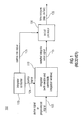
- Fig. 1 shows a block diagram of an embodiment of the receiver 100 for determining a time measure depending on a time of arrival of a pulse signal 105.
- the pulse signal 105 may be transmitted from a transmitter having a sequence of pulses.
- each pulse of the sequence of pulses may represent a band-limited pulse such as a UWB pulse.
- the receiver 100 is configured to receive the transmitted pulse signal or a preprocessed version (e.g. a squared version) thereof.
- the receiver 100 comprises an integrator 110, an integrator controller 120 and an output processor 130.
- the integrator 110 has a variable and controllable integration window, extending from a starting point to an integrator sampling point.
- the integrator controller 120 may be configured for controlling the integration window in a time-successive way so that the sampling points of successive integration windows are changed by a time delay from a current integration window to a later integration window.
- the time delay may be smaller than half of the integration window.
- the output processor 130 may be configured for generating the time measure 135 as an indication indicating which later integration window has a sampled integrator value exceeding a threshold.
- the indication may also be based on a comparison of the sampled integrator value with a sampled integrator value for a timely preceding or timely succeeding integration window.
- the integrator controller 120 may provide a control signal 121 for the integrator 110 and a control information 125 for the output processor 130.
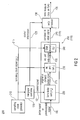
- Fig. 2 shows a block diagram of a further embodiment of the receiver 200 for determining a time measure depending on a time of arrival of a pulse signal in more detail.
- the receiver 200 of Fig. 2 essentially comprises the same blocks as the receiver 100 of Fig. 1 . Therefore; identical blocks having similar implementations and/or functions are denoted by the same numerals.
- the receiver 200 further comprises a sampling clock generator 210 for generating a sampling clock signal 215. It can be seen in Fig. 2 that the sampling clock generator 210 is connected to the integrator controller 120.
- the integrator controller 120 may be configured to introduce the time delay ⁇ t p based on the sampling clock signal 215.
- the integrator controller 120 may be set so that the time delay ⁇ t p will be introduced for each predetermined (N s + 1)th pulse of the sampling clock signal 215.
- the integrator 250 which may correspond to the integrator 110 of Fig. 1 , may be configured to integrate an original or delayed pulse signal 225 one time and not more than one time between two time adjacent clock events.
- the integrator 250 may be set so that the integration will be performed within a predefined integration window ⁇ t int being smaller than or equal to a sampling clock period ⁇ t s .
- the sampling clock period ⁇ t s is typically defined by a time distance between two time adjacent clock events provided by the sampling clock signal 215.
- an appropriate timing of the delay and integration operations such as within the integrator 250 can essentially be realized by using a same sampling clock signal (e.g. sampling clock signal 215) generated by the sampling clock generator 210.
- the integrator 250 of the receiver 200 may comprise a time delay unit 220 which is controlled by the integrator controller 120.
- the time delay unit 220 may be configured for delaying the pulse signal 105 by increasing time delays over several successive pulses based on a control signal 121 output by the integrator controller 120.
- the integrator 250 of the receiver 200 furthermore comprises an integration unit 230 and a sampling and hold device 240.
- the integration unit 230 is configured for integrating the original or delayed pulse signal 225 output by the time delay unit 220 to obtain an integration unit output signal 235, while the sampling and hold device is configured for sampling the integration unit output signal 235 output by the integration unit 230 to obtain a sampled integrator value signal 245.
- the sampled integrator value signal 245 output by the integrator 250 of Fig. 2 may correspond to the sampled integrator value signal 115 output by the integrator 110 of Fig. 1 .
- the output processor 130 may be configured to be operative on the sampled integrator value signal 245 to determine the time measure 135 based on the control information 125 provided by the integrator controller 120. More details of the individual processing blocks such as employed by the receivers 100; 200 will be described later.
- Figs. 3a; 3b; 3c; 3d show time plots of different exemplary processed signals 225, 235, 245, which are present at different processing stages such as within the receiver 200 of Fig. 2 .
- Fig. 3a the time plot of an exemplary original or preprocessed pulse signal 325-1 is shown.
- the original or preprocessed pulse signal 325-1 shown in Fig. 3a may correspond to the original or delayed pulse signal 225 output by the time delay unit 220 shown in Fig. 2 .
- the original or preprocessed pulse signal 325-1 may, for example, be a UWB pulse after a squaring operation.
- an original or preprocessed pulse signal (325-1; 225) representing a squared signal obtained after a squaring operation is to be integrated.
- the vertical axis of a time plot represents a level (e.g. energy or power) of a processed signal
- the horizontal axis of a time plot represents the time, respectively.
- the time may be defined with reference to a sampling clock signal having a sampling clock period ⁇ t s .
- the original or preprocessed pulse signal 325-1 of Fig. 3a extends from a starting point 301 to an end point 303, wherein the starting and the end point 301, 303 may, for example, be defined with respect to or corresponding to two time adjacent clock events provided by the sampling clock signal 215.
- the original or preprocessed pulse signal 325-1 of Fig. 3a is essentially identical to the pulse signal 105 input to the time delay unit 220 of Fig. 2 . This is because in case the original or preprocessed pulse signal is provided, the pulse signal 105 is directly fed to the output of the time delay unit 220 without application of a time delay to the same.
- a time plot of an exemplary delayed pulse signal 325-2 with a time delay ⁇ t p is shown.
- the exemplary delayed pulse signal 325-2 shown in Fig. 3b may correspond to the original or delayed pulse signal 225 shown in Fig. 2 .
- the delayed pulse signal 325-2 essentially corresponds to a pulse signal or preprocessed signal 105, which has been delayed by the time delay ⁇ t p using the time delay unit 220 of Fig. 2 .
- the time delay ⁇ t p is smaller than half of the integration window ⁇ t int .
- a size of the integration window ⁇ t int may correspond to the sampling period ⁇ t s defined by a time interval extending from the starting point 301 to the end point 303.
- Fig. 3c shows two time plots of integration unit output signals 335-1, 335-2 based on the exemplary original (or preprocessed) or delayed pulse signal of Fig. 3a and Fig. 3b , respectively.
- the integration unit output signals 335-1, 335-2 shown in Fig. 3c may correspond to the integration unit output signal 235 at the output of the integration unit 230 shown in Fig. 2 .
- the time plot 335-1 of Fig. 3c may be obtained from an integration of the original or preprocessed pulse signal 325-1 of Fig. 3a
- the time plot 335-2 of Fig. 3c may be obtained from an integration of the delayed pulse signal 325-2 of Fig. 3b , respectively, wherein the integration is performed within the integration window ⁇ t int corresponding to the sampling clock period ⁇ t s . It can be seen in Fig.
- the integration unit output signal 335-1, 335-2 may have a rising portion 337-1, 337-2 extending from a starting point 301 to a characteristic time t s and a trailing portion 339-1, 339-2 extending from the characteristic time t s to an end point 303 of the integration window ⁇ t int .
- the rising and trailing portions of the integration unit output signal typically originate from an alternate switching between an integrating or activated state and a non-integrating or deactivated state of the integration unit. As shown in Figs.
- the integration window for the original or preprocessed pulse signal 325-1 and the delayed pulse signal 325-2 extends at least partially from a starting point 301 to an integrator sampling point 305-1 (P s1 ) and 305-2 (P s2 ), respectively, wherein the integrator sampling points 305-1, 305-2 are changed by the time delay ⁇ t p with respect to the corresponding pulse shape from the original or preprocessed pulse signal 325-1 to the delayed pulse signal 325-2. Therefore, as shown in Fig. 3c , the integration unit output signal 335-2 corresponding to the delayed pulse signal 325-2 will essentially be higher than the integration unit output signal 335-1 corresponding to the original or preprocessed pulse signal 325-1 over the whole integration window.
- Fig. 3d shows two time plots of sampled integrator value signals 345-1, 345-2 based on the integration unit output signals of Fig. 3c .
- the sampled integrator value signals 345-1, 345-2 may be output by the sampling and hold device 240 of the receiver 200 shown in Fig. 2 .
- the sampled integrator value signals 345-1, 345-2 of Fig. 3d may correspond to the sampled integrator value signal 245 of Fig. 2 .
- the integration unit output signals 335-1, 335-2 may be sampled at the characteristic time t s corresponding to respective integrator sampling points 311-1, 311-2, wherein the integrator sampling points 311-1, 311-2 of Fig.
- sampled integrator value signals 345-1, 345-2 as shown in Fig. 3d may be obtained from sampling the integration unit output signals 335-1, 335-2 at the integrator sampling points 311-1, 311-2, respectively.
- the thus obtained sampled integrator value signals 345-1, 345-2 are typically not represented by single values in the time plots and may extend from a starting point 301 to an end point 303 within the sampling clock period ⁇ t s . This behavior is essentially due to a sampling and hold operation performed by a sampling and hold device such as the sampling and hold device 240 of Fig. 2 . It can be seen from Figs.
- the sampled integrator value signals 345-1, 345-2 essentially have different levels.
- the sampled integrator value signal 345-2 is characterized by a relatively large value, while the sampled integrator value signal 345-1 is characterized by a relatively low value.
- the characteristic time t s which characterizes the integrator sampling points may be chosen to be approximately located in the middle of the integration window ⁇ t int or sampling clock period ⁇ t s , respectively, wherein the time t s is measured with respect to a starting point defined by an initial clock event (i.e. t s ⁇ 1 ⁇ 2 ⁇ ⁇ t int ).
- the two sampled integrator value signals 345-1, 345-2 can essentially be used to distinguish between the corresponding original or preprocessed pulse signal 325-1 and the delayed pulse signal 325-2.
- this processing can be extended to a plurality of different sampled integrator value signals corresponding to different successively introduced time delays ⁇ t t .
- the successively introduced time delay ⁇ t p is smaller than half of the integration window ⁇ t int for each introducing the same.
- Fig. 4 shows a block diagram of an embodiment of a time delay unit 400 using a control signal.
- the time delay unit 400 of Fig. 4 may correspond to the time delay unit 220 of Fig. 2 .
- the other identical blocks in Fig. 2 and Fig. 4 having similar implementations and/or functions are denoted by the same numerals.
- the time delay unit 400 of Fig. 4 may comprise a plurality 401 of delay lines for successively processing the pulse signal 105 and for feeding the successively processed signal 405-1, 405-2, ..., to the output 455 of the time delay unit 400, respectively.
- the output 455 of the time delay unit 400 may correspond to the output 225 of the time delay unit 220 for the original or delayed pulse signal.
- Fig. 4 shows a block diagram of an embodiment of a time delay unit 400 using a control signal.
- the time delay unit 400 of Fig. 4 may correspond to the time delay unit 220 of Fig. 2 .
- the plurality 401 of delay lines comprises a changing number of individual delay line elements 410-1, 410-2, ..., wherein each individual delay line element 410-1, 410-2, ..., is configured to introduce a time delay ⁇ t p .
- each individual delay line element 410-1, 410-2, ... is connected with a switch output 422, 426 of a preconnected switch 420-1, 420-2 and a switch input 424, 428 of a post-connected switch 420-2, 420-3, respectively.
- the plurality of switches 420-1, 420-2, 420-3 is especially configured to perform a switching based on the control signal 121.
- the switching in particularly performed such that, for an initial sampling period I, the pulse signal 105 will directly be fed to the output 455 of the time delay unit 400, and for successive sampling periods II, III, ..., the pulse signal 105 will successively be processed by the plurality 401 of delay lines. In this way, the original or delayed pulse signal will be obtained at the output 455 of the time delay unit 400.
- the special configuration of the time delay unit 400 ensures that in case of identical delay line elements 410-1, 410-2, ..., for example, the pulse signal 105 will successively be delayed by the time delay ⁇ t p , while passing the corresponding delay lines 405-1, 405-2, ..., respectively.
- the pulse signal 105 is not delayed within the initial sampling period I, while it is successively delayed and accumulating increasing time delays (1 ⁇ ⁇ t p , 2 ⁇ ⁇ t p , ...) within the successive sampling periods II, III, ..., respectively.
- the controlled switching as indicated by the arrows showing the respective switching states of the switches 420-1, 420-1, 420-3 for the sampling periods I, II, III, ..., can especially be performed by using the integrator controller 120.
- the integrator controller 120 may be configured to provide the control signal 121 based on the sampling clock signal 215 generated by the sampling clock generator 210.
- the switches 420-1, 420-2, 420-3 can be controlled so that the switching from an initial path 411 to the successive delay lines 405-1, 405-2, ..., respectively, will coincide with several successive pulses of the sequence of pulses constituting the pulse signal 105. Therefore, according to the embodiment of Fig.
- an original pulse of the sequence of pulses will directly be fed to the output 455 of the time delay unit 400 without being delayed, a successive pulse of the sequence of pulses will be delayed by a time delay ⁇ t p , yet a successive pulse will be delayed by two times the time delay (2 ⁇ ⁇ t p ) etc.
- the time delay ⁇ t p of each delay line element 410-1, 410-2, ... may, for example, be set to a fraction 1/N ⁇ ⁇ t of the integration window ⁇ t int , wherein N corresponds to the number of the plurality 401 of delay lines or the successive pulses of the sequence of pulses, respectively, received by the time delay unit 400.
- Fig. 5 shows a block diagram of a an embodiment of an integrator controller 500 with a comparator for providing a control signal and a control information for the output processor such as employed by the receiver 100 of Fig. 1 .
- the integrator controller 500 may comprise a counter 510 for counting pulses of a sampling clock signal 215 to obtain a counter output signal 515.
- the integrator controller 500 may furthermore comprise a comparator 520 which is configured to provide a control signal 521 for the integrator 110.
- the control signal 521 shown in Fig. 5 essentially corresponds to the control signal 121 of the receiver 100 shown in Fig. 1 .
- control signal 521 can be based on a comparison of a counter output signal 515 with a predetermined threshold 501.
- the comparator 520 is also configured to provide a counter reset signal 523 for resetting the counter 510 when the predetermined threshold 501 is reached.
- the predetermined threshold 501 may, for example, be reached for each N s th pulse of the sampling clock signal 215.
- the integrator 110 such as shown in the Fig. 1 embodiment can be controlled by the control signal 521, so that the time delay ⁇ t p will be introduced for each (N s + 1)th pulse of the sampling clock signal 215.
- the comparator 520 of Fig. 5 is furthermore configured to generate a control information 525, which may correspond to the control information 125 as shown in Fig. 1 , wherein the control information 525 indicates different delays to be used for the output processor 130.
- the different delays are obtained from successively introducing the time delay ⁇ t p , respectively.
- the comparator 520 of the integrator controller 500 may provide the control signal 521 especially for the time delay unit comprising the plurality 401 of delay lines.
- the control signal 521 may be supplied to the plurality of switches 420-1, 420-2, 420-3 which are controlled so that the original or delayed pulse signal 455 will be obtained for the initial sampling period I and the successive sampling periods II, III, ..., respectively.
- no time delay (delay line 411) or accumulated different time delays (1 ⁇ ⁇ t p , 2 ⁇ ⁇ t p , ...) will successively be introduced by the plurality 401 of delay lines. This has been described correspondingly before.
- each sampling period I, II, III, ... corresponds to a number N s of consecutive pulses indicated by 1, 2, ..., N s of the sampling clock signal 215.
- the thus defined sampling periods I: 1, 2, ..., N s ; II: 1, 2, ..., N s ; ... are obtained because of the threshold condition (arrow 501) used by the comparator 520.
- the control information 525 is also provided by the comparator 520 of the integrator controller 500.
- control information 525 may comprise an indication of the absence of a time delay for the initial sampling period (I: 1, 2, ..., N s ) or the accumulated different delays (1 ⁇ ⁇ t p , 2 ⁇ ⁇ t p , ...) for the successive sampling periods (II: 1, 2, ..., N s , III: 1, 2, ..., N s , ...), respectively.
- This control information may subsequently be used by the output processor for generating a time measure.
- the integrator 250 may comprise an integration unit 230 for integrating an original or delayed pulse signal 225 in an integration window ⁇ t int , wherein the integrator 250 is particularly configured to perform the following steps. First, the starting point to of the integration window ⁇ t int is determined dependent on a sampling clock event. Then, an integrator value is sampled at the integrator sampling point t s a time period later than the starting point to. Here, the time period is smaller than a sampling clock period t s . Finally, the integrator 250 is reset subsequent to the sampling point t s .
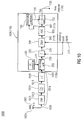
- Fig. 6 shows a block diagram of an embodiment of a resister capacitor (RC) integration unit 600 with a switch.
- the resistor capacitor integration unit 600 which may correspond to the integration unit 230 of Fig. 2 , comprises a switch 630, wherein the switch 630 is configured to switch between an integrating and a non-integrating state of the integration unit 600 with respect to a sampling clock period ⁇ t s .
- the RC integration unit 600 may consist of a resistor 610 denoted by 'R' and a capacitor 620 denoted by 'C' which are connected in such a way that an incoming signal (e.g.
- the incoming signal of the RC integration unit 600 may correspond to the original or delayed pulse signal 455 (225) provided by the time delay unit 400 of Fig. 4 or the time delay unit 220 of Fig. 2 , respectively, while the output signal 635 may correspond to the integration unit output signal 235 of Fig. 2 .
- the switch 630 of the RC integration unit 600 can be controlled by a sampling clock signal such as the sampling clock signal 215 generated by the sampling clock generator 210 of Fig. 2 , wherein an open state of the switch 630 may correspond to the integrating state, while a closed state of the switch 630 may correspond to the non-integrating state.
- a time plot of an exemplary integration unit output signal 635 which may correspond to the integration unit output signal 335-1 or 335-2, respectively, is also shown. It can be seen in the time plot of Fig. 6 that in the integrating state of the switch 630, a level of the integration unit output signal 635 increases corresponding to a charging of the capacitor 620, while in the non-integrating state of the switch, the level of the integration unit output signal 635 decreases corresponding to a discharging of the capacitor 630.
- the time period 655-1, 655-2 for the integrating state and the non-integrating state, respectively, may be controlled by the switch 630 so that the time period 655-1 will extend from an initial sampling clock event to to an integrator sampling time t s , while the time period 655-2 will extend from the integrator sampling time t s to a consecutive sampling clock event to + ⁇ t s , wherein ⁇ t s is the sampling clock period as provided by the sampling clock signal 215.
- the integration window ⁇ t int may be defined by the two time adjacent clock events to and to + ⁇ t s .
- the integrator (250) may comprise a sampling and hold device (240) for sampling an integration unit output signal (235).
- the sampling and hold device (240) may be configured for generating the sampled integrator value signal (245) by sampling the integration unit output signal (235) at the integrator sampling point (t s ).
- Fig. 7 shows a block diagram of an embodiment of an output processor with a threshold selector and a time of arrival calculator.
- the output processor 700 shown in Fig. 7 may correspond to the output processor 130 of the receiver 100 shown in Fig. 1 .
- the output processor 700 may comprise a value selector 710, the threshold selector 720, a comparator 722 and a time of arrival (ToA) calculator 730.
- the output processor 700 is configured to receive a sampled integrator value signal 705, which may correspond to the sampled integrator value signal 115 provided by the integrator 110 of Fig. 1 .
- the sampled integrator value signal 705 may, for example, be a digital signal having been obtained after an analog-to-digital conversion of an analog sampled integrator value signal.
- the value selector 710 of the output processor 700 may be configured for selecting a plurality of sampled integrator values for a predefined consecutive sampling block 711 and for relating the selected sampled integrator values to corresponding delays indicated by a control information 125 from the integrator controller 120. In this way, the distribution 715 of sampled integrator values will be obtained at the output of the value selector 710.
- the predefined consecutive sampling block 711 may, for example, be defined by a sampling clock period ⁇ t s having a same indication within different successive sampling periods.
- the predefined consecutive sampling block 711 may correspond to a specific time period extending between two repeated time adjacent clock events for different successive sampling periods, wherein the predefined consecutive sampling block 711 can, for example, be the ith consecutive sampling block corresponding to the ith sampling clock event of the initial sampling period I, a successive sampling period II, etc.
- the distribution 715 of sampled integrator values may comprise the selected sampled integrator values of the ith consecutive sampling block related to the corresponding accumulated time delay (1 ⁇ ⁇ t p , 2 ⁇ ⁇ t p , ...) obtained after the successive time delay operation as described in detail before.
- the threshold selector 720 may be operative on the distribution 715 of sampled integrator values to obtain a selected threshold 721.
- the threshold selection performed by the threshold selector 720 may be based on a statistical analysis, or more specifically, on a probability characteristic of the distribution 715 of sampled integrator values such as a kurtosis estimate of the same.
- the comparator 722 of the output processor 700 may be configured for determining a specific delay 725 for which a sampled integrator value exceeds the selected threshold 721.
- the specific delay 725 can be determined based on a comparison of the distribution 715 of sampled integrator values with the selected threshold 721.
- the time of arrival (ToA) calculator 730 may be configured for calculating a time of arrival 735 of the pulse signal based on the determined specific delay 725.
- the calculation of the ToA 735 performed by the ToA calculator 730 may be based on the information about the predefined consecutive sampling block 711, wherein the ToA can be calculated with respect to a specific clock event corresponding to the ith consecutive sampling block. If, for example, the ith consecutive sampling block has a frame border at 7ns, while a determined specific delay corresponding to 3 ⁇ ⁇ t p is obtained, the ToA will be estimated to be approximately 7.3 ns. The estimated ToA can then be used to estimate a corresponding time measure 135.
- Fig. 8 shows a graph of an exemplary distribution 800 of sampled integrator values, which may correspond to the distribution 715 as processed by the output processor in accordance with Fig. 7 .
- selected sampled integrator values 805 of the distribution 800 are depicted versus the corresponding delays in units of ⁇ t p .
- the vertical axis of the distribution represents the received signal energy
- the horizontal axis of the distribution represents an indication indicating a current 810 and later integration windows 815.
- the current and the later integration windows 810, 815 are separated from each other by the time delay ⁇ t p , respectively, wherein the time delay ⁇ t p is exemplarily set to 1/Nth of the integration window ⁇ t int , so that N shifts of the integration window or successively introduced time delays will result in an overall shift being equal to the integration window ⁇ t int .
- the time delay ⁇ t p corresponds to 1/8 th of the integration window. It can be clearly seen in Fig. 8 that the specific delay 725 for which a sampled integrator value 825 exceeds the selected threshold 721 corresponds to the indication "5" representing the ToA of the pulse (ToA p ) to be used for the time measure 135.
- the indication "5" in the example of Fig. 8 indicates that the fifth later integration window corresponding to an accumulated delay of 5 ⁇ ⁇ t p has a sampled integrator value exceeding the threshold, thereby identifying the time of arrival of the pulse with respect to the current integration window.
- Fig. 9 shows a block diagram of an embodiment of an analog-to-digital converter 900 (ADC) placed between an integrator and an output processor.
- the analog-to-digital converter 900 ADC may be configured for converting an analog signal 915 output by the integrator 110 into a digital signal 917 for the output processor 130.
- the analog signal 915 and the digital signal 917 may correspond to the sampled integrator value signal 115 as shown in the Fig. 1 embodiment.
- the integrator 110 is especially configured as an analog circuit 910, while the output processor 130 is especially configured as a digital circuit 930.
- the integrator 910 and the output processor 930 as shown in Fig. 9 may correspond to the integrator 110 and the output processor 130 as shown in Fig. 1 .
- the analog-to-digital converter 900 essentially represents an interface between the analog part and the digital part of a receiver.
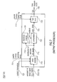
- Fig. 10 shows a block diagram of a further embodiment of a receiver 1000 for determining a time measure depending on a time of arrival of a pulse signal.
- the receiver 1000 comprises a preprocessing unit 1010 and an integrator 1020, which may correspond to the integrator 110 with the variable and controllable integration window as shown in Fig. 1 .
- the integrator 1020 essentially comprises the same blocks as has been described in the previous embodiments. Therefore, identical blocks having similar implementations and/or functions are denoted by the same numerals.
- the preprocessing unit 1010 may be configured for preprocessing a raw signal 1005 output by an antenna 1001.
- the antenna 1001 can be used for receiving a UWB signal from a transmitter and to generate the raw signal 1005.
- the preprocessing unit 1010 comprises a low noise amplifier 1012 (LNA), a filter 1014 and a squaring device 1016. After a preprocessing by the preprocessing unit 1010, an output signal 1055 will be obtained.
- the output signal 1055 provided by the preprocessing unit 1010 may correspond to the pulse signal or preprocessed signal 105 to be used by the integrator 1020.
- the processing blocks of the preprocessing unit 1010 may work in the following way.
- the LNA 1012 is configured to amplify the raw signal 1005 to obtain an amplified signal 1013.
- the filter 1014 is configured to be operative on the amplified signal 1013 to generate a filtered signal 1015.
- the filtered signal 1015 may be obtained by applying a bandpass filter to the amplified signal 1013.
- the squaring device 1016 is configured to perform a squaring operation of the filtered signal 1015 to obtain a squared signal 1055 as an input for the integrator 1020. Subsequently, the integrator 1020 is operative on the squared signal 1055 to determine the ToA 735 of the pulse signal as described in detail before.
- Fig. 11 shows a schematic illustration of an exemplary UWB ranging system 1100 according to another embodiment of the present invention.
- a developed UWB ranging platform may consist of a transmitter 1110, a receiver 1120, and a trigger unit 1130.
- a high level block diagram of the platform is shown in Fig. 11 .
- a transmitter 1110 a Picosecond 3500D Pulse generator is used. It is able to produce an ultra short pulse of a full width of 65 ps at half the maximum (fwhm) and of an amplitude of 8 V that is repeated with the repetition rate of 0.5 MHz.
- the trigger unit 1130 that provides the time synchronization signal between the transmitter 1110 and the receiver 1120, consists of a Tektronix AWG 7122B Arbitrary Waveform Generator 1132 and an Analog Devices AD9516 PLL evaluation board 1134 that adjusts the trigger signal 1135 in frequency and amplitude as required by the Picosecond generator 1110 and the oscilloscope 1120.
- a LeCroy WE100H 30 GS/s sampling oscilloscope is used as receiver 1120.
- the unknown distance 1115 between the two UWB SMT-3TO10M-A SkyCross antennas 1112, 1118 operating in the 3-10 GHz band is determined by means of a ToA method that is based on measuring the propagation time.
- the two UWB antennas 1112, 1118 are mounted on a rail guide allowing for distance change and are connected to the measurement equipment via high quality Sucoflex 104PE cables. These cables have the S21 parameter for frequencies ⁇ 12 GHz being better than -1.1 dB and -1.7 dB for 1m and 1.5 m cable length, respectively. All signal processing operations at the receiver side, i.e., signal squaring, integration, and A/D conversion, threshold selection, and distance calculation are performed by a Visual Basic application operating in real-time on the sampling oscilloscope 1120. Visual Basic support is one of the custom features of LeCroy oscilloscopes that allows to create and deploy a measurement or algorithm directly on the oscilloscope in real-time.
- GUI graphical user interface
- Figs. 12a; 12b; 12c; 12d; 12e show time plots of different exemplary signals employed by the previous embodiments and related to the UWB ranging system 1100 of Fig. 11 .
- Fig. 12a a time plot of an exemplary sampling clock signal 1200 from a sampling clock generator is shown.
- the individual sampling pulses of sampling clock events of the sampling clock signal 1200 may be indicated by "1", “2", “3", “4", ..., "N s " within an initial sampling period I: 1...N s and the successive sampling periods II: 1...N s , III: 1...N s , ..., respectively.
- the time period between two time adjacent clock events e.g.
- sampling clock period ⁇ t s wherein the individual pulses of the sampling clock signal 1200 may be equally spaced.
- a time plot of an exemplary transmitted pulse signal 1220 indicated by "T" having a sequence of pulses is shown.
- the individual pulses 1222, 1224, 1226 of the sequence of pulses also referred to as 'pulse repetitions' may be equally spaced with respect to each other having a repetition time period ⁇ t rep .
- This means that the individual pulses 1222, 1224, 1226 may be repeated for each (N s + 1)th pulse of the sampling clock signal 1200 (i.e. approximately for each 1001th pulse in the above example).
- Fig. 12c shows a time plot of an exemplary received pulse signal 1240 indicated by "R" having been delayed by increasing time delays over several successive pulses.
- the exemplary received pulse signal 1240 of Fig. 12c is time delayed or shifted with respect to the exemplary transmitted pulse signal 1220 of Fig. 12b .
- the time delay between the transmitted and the received pulse signal essentially corresponds to a propagation time or the ToA of the pulse signal propagating between a transmitter and a receiver.
- the individual time delayed pulses 1242, 1244, 1246 of the exemplary received pulse signal 1240 are indicated by dotted lines.
- the transmitter and the receiver are well synchronized at least within a relevant analysis time (e.g. about 10 ⁇ s), or for a sufficiently large number of pulse repetitions (e.g. up to 10 pulse repetitions).
- the received pulse signal 1240 essentially comprises a plurality of successively delayed pulses 1245, 1247, ..., which have been furthermore delayed by increasing time delays (1 ⁇ ⁇ tp, 2 ⁇ ⁇ t p , ...) with respect to the corresponding time delayed pulses 1244, 1246, ... of the received pulse signal 1240.
- Fig. 12d shows a time plot of an exemplary integration unit output signal 1260 based on the exemplary received pulse signal of Fig. 12c .
- the individual signals 1262, 1264, 1266... of the integration unit output signal 1260 may be obtained by integrating the individual signals 1242, 1245, 1247, respectively, as described in the previous embodiments. It can be seen in Fig. 12d that the individual signal 1264 has a larger value than the timely preceding or timely succeeding individual signals 1262, 1266.
- Fig. 12e shows a time plot of an exemplary sampled integrator value signal 1280 based on the exemplary integration unit output signal of Fig. 12d .
- the sampled integrator value 1284 exceeds a selected threshold 721, while the timely adjacent sampled integrator values 1282, 1286 are below the threshold 721.
- the specific delay for which the sampled integrator value 1284 exceeds the threshold 721 is 1 ⁇ ⁇ t p corresponding to the indication "1".
- the indication "1" obtained by comparing the sampled integrator values for the third consecutive block of the sampling clock periods I, II, III, ... with the threshold would correspond to a ToA of approximately 2.1 ns.
- Fig. 13 shows a schematic illustration of a further embodiment of a receiver 1300 for determining a localization of the same.
- the receiver 1300 may comprise a plurality 1310 of inventive receivers a position calculator 1320.
- the plurality 1310 of inventive receivers may be configured for determining at least two different ToAs 1315 of pulse signals 1305 each having a sequence of pulses from a plurality of transmitters.
- the position calculator 1320 may be configured for calculating a current position 1325 of the receiver 1300 depending on the at least two different ToAs 1315.
- the calculation of the current position 1325 by the position calculator 1320 may, for example, be performed with a localization or triangulation procedure, which is based on the positions of the plurality of transmitters and respective radial distance information depending on the at least two different ToAs.
- Fig. 14 shows time plots of an exemplary real measured squared 1410 and integrated signals 1420 with a threshold 1405 such as obtained with the UWB ranging system of Fig. 11 .
- the integration and sampling operation has been performed according to the prior art with an exemplary sampling rate of 2 GS/s corresponding to a sampling clock period of 0.5 ns (see signal 1420 after the integration).
- Fig. 15 shows a graph of an exemplary mean absolute error (MAE), illustrating a performance of the exemplary UWB ranging system of Fig. 11 according to an embodiment of the present invention.
- the performance of such an inventive ranging system in terms of the mean absolute error (MAE) is presented in Fig. 15 .
- the MAE 1510 is in the centimeter range for integration window sizes of 1 ns and 2 ns, which corresponds to sampling rates of 1GS/s and 500 MS/s, respectively.
- the mean absolute error (MAE) 1510 is shown in Fig. 15 for the integration window sizes of 1 and 2 ns with 20 and 40 acquisitions.
- a UWB signal is received by the UWB antenna and amplified by the low noise amplifier (LNA). Next, it is filtered and squared ( ⁇ ) 2 . The resulting signal is integrated over a defined time which is called the integration window size.
- embodiment of the present invention are realized by shifting the windows by a small time ⁇ t p . This requires N signal acquisitions and hence a N repetitions of the UWB signal.
- the element responsible for shifts of the integration window is the time delay unit.
- the analog-to-digital conversion is performed.
- the digital values of the signal energy contained in every window are compared against the threshold.
- the threshold itself may be selected based on a signal kurtosis estimate (such as in US 7,526,048 B2 ).
- the integration window of which the signal energy is above the threshold is selected and determines the ToA and also the estimated distance.
- the sampling can be performed in the middle of the integration window.
- the present invention has been described in the context of block diagrams where the blocks represent actual logical hardware components, the present invention can also be implemented by a computer-implemented method. In the latter case, the blocks represent corresponding method steps where these steps stand for the functionalities performed by the corresponding logical or physical hardware blocks.
- the inventive methods can be implemented in hardware or in software.
- the implementation can be performed using a digital storage medium, in particular disk, a DVD or CD having electronically, readable control signals stored thereon, which cooperate with programmable computer systems, such that the inventive methods are performed.
- the present invention can, therefore, be implemented as a computer program product with the program code stored on a machine readable carrier, the program code being operative for performing the inventive methods when the computer program product runs on a computer.
- the inventive methods are, therefore, a compute program having a program code for performing at least one of the inventive methods when the computer program runs on a computer.
- An inventive signal can be stored on any machine-readable storage medium, such as a digital storage medium.
- Embodiments of the present invention provide a solution for avoiding a poor time resolution and related with it a relatively large ToA estimation error of the ED.
- An advantage of the present invention is that a high time- and thus distance-resolution ranging can be preformed with only one AD converter in the ED receiver and with realistic sampling rate of 1 GS/s or 500 MS/s. Moreover, no a-priori knowledge about the channel or about the signal is required. Therefore, embodiments of the present invention provide a structure of a receiver which is relatively simple and feasible.
- a matched filter/correlation receiver In a conventional matched filter/correlation receiver, the knowledge of the received pulse that is required for this type of receiver may not be available in practice. Moreover, the waveform distortion induced by the near-field coupling between antenna and the propagation environment poses challenges on the accurate waveform representation in the receiver. As opposed to such a matched filter receiver, embodiments of the present invention may not require a Nyquist or higher rate sampling, and as a result, it will be feasible for low cost UWB devices. In the art, however, for a signal bandwidth of 2 GHz, a sampling rate of at least 4 GS/s is needed.
- c 10 8 m/s is the speed of light.
- the present invention relates to an architecture of an energy detection receiver, which enables high resolution ranging via a time-of-arrival technique.
- the present invention is advantageous because it does not require any a-priori knowledge about neither the receive pulse shape nor the channel and yet can achieve good results with lower sampling rates.
- Embodiments of the present invention therefore provide a technique to achieve a centimeter accuracy using a non-coherent energy detection receiver in a ToA UWB ranging system.
- the presented technique allows for such a performance with the sampling rate as low as 1 GS/s or even 500 MS/s.
Abstract
Description
- Embodiments of the present invention relate to wireless ultra-wideband (UWB) ranging and localization systems, and in particular, to a concept for determining a time measure depending on a time of arrival of a pulse signal having a sequence of pulses from a transmitter. Further embodiments of the present invention relate to an energy receiver architecture for UWB ToA (time of arrival) estimation.
- Ultra-wideband Impulse Radio (UWB-IR) has several unique characteristics that make it a promising candidate for future wireless localization. The large absolute bandwidth, in the US from 3.1 to 10.6 GHz and in Europe from 6 to 8.5 GHz, corresponds to a very fine time resolution in the order of hundreds of picoseconds which translates to spatial resolution in the order of centimeters. The very fine time resolution allows a direct path to be easily distinguished from the reflected paths. This is of paramount importance in indoor environments where other localization systems suffer from the multipath phenomenon. The presence of low frequency components in the UWB signal spectrum enables penetration of the UWB signals through the walls. UWB devices are permitted to transmit very weak signals so that other systems sharing the same spectrum, including for instance IEEE 802.11a WLANs, are protected. Low interference, possibility of high device density and low probability of detection and interception (LPD/I) are these characteristics of the UWB technology that are of particular importance for military applications. Furthermore, the UWB technology promises prospects for long-life battery operation and low cost mainly thanks to simple transceiver implementations.
- However, the same properties provide design challenges, such as high sampling rate, synchronization and power control. Portable devices impose strict requirements on the size and shape of the antenna which has to radiate effectively in a wide frequency band and under varying propagation conditions sometimes including near-field, e.g. when carried on the human body or close objects. To ensure a further development of the UWB technology and a wide presence of its products on the commercial market of tomorrow, these challenges must be properly addressed and resolved.
- Reception of UWB signals poses challenges in the receiver structure. According to the state-of-the-art, an optimal estimate of ToA may be performed by means of a conventional matched filter / correlation receiver.
- An example of a correlating receiver is presented in
US 2005/0069059 A1 , where the use of a pulse sequence energy estimator and a complicated architecture is required.US 2003/0227961 Al describes a RAKE architecture for an UWB receiver. The architecture is based on a bank of switched capacitors and requires high sampling rate. - A low complexity alternative to the matched filter or RAKE receiver is the energy detection (ED) receiver.
WO 2005/074150 Al presents a non-coherent receiver based on the ED architecture that is suitable for communication applications with PAM (pulse amplitude modulation) and PPM (pulse position modulation) schemes. Here, it is proposed to perform a weighting integration operation.US 7.526.048 B2 describes a method for selecting the threshold in the ED-receiver based ToA ranging system. It is proposed to use kurtosis of the signal after an integration step in the ED. Another method of setting the threshold is presented in Ismail Guvenc and Zafer Sahinoglu, "Threshold-Based TOA Estimation for Impulse Radio UWB Systems", IEEE International Conference on Ultra-Wideband. ICU 2005. This method is based on normalized value according to the signal-to-noise value and integration window size. - However, a general problem of known receivers is that they are characterized by relatively low time/distance resolution and have a relatively complex structure.
- It is, therefore, an object of the present invention to provide an improved concept of a receiver, which on the one hand, allows for an increased time/distance resolution, and on the other hand, allows for an efficient implementation.
- This object is achieved by a receiver according to
claim 1, a method according to claim 15, a receiver according to claim 14, a method according to claim 16 and a computer program according to claim 17. - According to an embodiment of the present invention, the receiver for determining a time measure depending on a time of arrival of a pulse signal having a sequence of pulses from a transmitter comprises an integrator, an integrator controller and an output processor. In particular, the integrator has a variable and controllable integration window, extending from a starting point to an integrator sampling point. The integrator controller is configured for controlling the integration window in a time-successive way so that the sampling points of successive integration windows are changed by a time delay from a current integration window to a later integration window, wherein the time delay is smaller than half of the integration window. The output processor is configured for generating the time measure as an indication indicating which later integration window has a sampled integration value exceeding a threshold or being larger than a sampled integrator value for a timely preceding or timely succeeding integration window.
- The basic idea underlying the present invention is that the above-mentioned higher resolution and/or efficient implementation can be achieved when a variable and controllable integration window is provided, extending from a starting point to an integrator sampling point, and the integration window is controlled in a time-successive way so that the sampling points of successive integration windows are changed by a time delay from a current integration window to a later integration window, wherein the time delay is smaller than half of the integration window. By this measure, a poor time resolution and a corresponding relatively large time of arrival estimation error can be prevented with relatively low effort, thereby realizing an improved concept of an efficient receiver.
- According to a further embodiment of the present invention, the integrator comprises a time delay unit controlled by the integrator controller, wherein the time delay unit is configured for delaying the pulse signal by increasing time delays over several successive pulses based on a control signal output by the integrator controller. This measure enables to controllably increase the time resolution, which essentially depends on how often time delays have been successively introduced.
- In the following, embodiments of the present invention are explained with reference to the accompanying drawings in which:
- Fig. 1
- shows a block diagram of an embodiment of the receiver for determining a time measure depending on a time of arrival of a pulse signal;
- Fig. 2
- shows a block diagram of a further embodiment of the receiver for determining a time measure depending on a time of arrival of a pulse signal in more detail;
- Fig. 3 a
- shows a time plot of an exemplary original or preprocessed pulse signal;
- Fig. 3b
- shows a time plot of an exemplary delayed pulse signal with a time delay (Δtp);
- Fig. 3c
- shows two time plots of integration unit output signals based on the exemplary original or delayed pulse signal of
Fig. 3a and Fig. 3b , respectively; - Fig. 3d
- shows two time plots of sampled integrator value signals based on the integration unit output signals of
Fig. 3c ; - Fig. 4
- shows a block diagram of an embodiment of a time delay unit using a control signal;
- Fig. 5
- shows a block diagram of an embodiment of an integrator controller with a comparator for providing a control signal and a control information to be used for an output processor of the receiver;
- Fig. 6
- shows a block diagram of an embodiment of a resistor capacitor (RC) integration unit with a switch;
- Fig. 7
- shows a block diagram of an embodiment of an output processor of the receiver with a threshold selector and a time of arrival calculator;
- Fig. 8
- shows a graph of an exemplary distribution of sampled integrator values processed by the output processor in accordance with
Fig. 7 ; - Fig. 9
- shows a block diagram of an embodiment of an analog-to-digital converter (ADC) placed between an integrator and an output processor of the receiver;
- Fig. 10
- shows a block diagram of a further embodiment of the receiver for determining a time measure depending on a time of arrival of a pulse signal derived from a UWB signal;
- Fig. 11
- shows a schematic illustration of an exemplary UWB ranging system according to an embodiment of the present invention;
- Fig. 12a
- shows a time plot of an exemplary sampling clock signal from a sampling clock generator;
- Fig. 12b
- shows a time plot of an exemplary transmitted pulse signal having a sequence of pulses;
- Fig. 12c
- shows a time plot of an exemplary received pulse signal having been delayed by increasing time delays over several successive pulses;
- Fig. 12d
- shows a time plot of an exemplary integration unit output signal based on the exemplary received pulse signal of
Fig. 12c ; - Fig. 12e
- shows a time plot of an exemplary sampled integrator value signal based on the exemplary integration unit output signal of
Fig. 12d ; - Fig. 13
- shows a schematic illustration of a further embodiment of a receiver for determining a localization of the same;
- Fig. 14
- shows time plots of exemplary real measured squared and integrated signals with a threshold according to the prior art;
- Fig. 15
- shows a graph of an exemplary mean absolute error (MAE), illustrating a performance of the exemplary UWB ranging system of
Fig. 11 according to an embodiment of the present invention; and - Fig. 16
- shows a graph of an exemplary distribution of sampled integrator values according to the prior art.
-
Fig. 1 shows a block diagram of an embodiment of thereceiver 100 for determining a time measure depending on a time of arrival of apulse signal 105. Thepulse signal 105 may be transmitted from a transmitter having a sequence of pulses. Here, each pulse of the sequence of pulses may represent a band-limited pulse such as a UWB pulse. Thereceiver 100 is configured to receive the transmitted pulse signal or a preprocessed version (e.g. a squared version) thereof. As shown inFig. 1 , thereceiver 100 comprises anintegrator 110, anintegrator controller 120 and anoutput processor 130. In particular, theintegrator 110 has a variable and controllable integration window, extending from a starting point to an integrator sampling point. Theintegrator controller 120 may be configured for controlling the integration window in a time-successive way so that the sampling points of successive integration windows are changed by a time delay from a current integration window to a later integration window. Here, the time delay may be smaller than half of the integration window. At the output of theintegrator 110, the sampledintegrator value signal 115 will be obtained. Theoutput processor 130 may be configured for generating thetime measure 135 as an indication indicating which later integration window has a sampled integrator value exceeding a threshold. Here, the indication may also be based on a comparison of the sampled integrator value with a sampled integrator value for a timely preceding or timely succeeding integration window. In the embodiment ofFig. 1 , theintegrator controller 120 may provide acontrol signal 121 for theintegrator 110 and acontrol information 125 for theoutput processor 130. -
Fig. 2 shows a block diagram of a further embodiment of thereceiver 200 for determining a time measure depending on a time of arrival of a pulse signal in more detail. Thereceiver 200 ofFig. 2 essentially comprises the same blocks as thereceiver 100 ofFig. 1 . Therefore; identical blocks having similar implementations and/or functions are denoted by the same numerals. In addition, thereceiver 200 further comprises asampling clock generator 210 for generating asampling clock signal 215. It can be seen inFig. 2 that thesampling clock generator 210 is connected to theintegrator controller 120. In embodiments, theintegrator controller 120 may be configured to introduce the time delay Δtp based on thesampling clock signal 215. - Specifically, the
integrator controller 120 may be set so that the time delay Δtp will be introduced for each predetermined (Ns + 1)th pulse of thesampling clock signal 215. - Referring to
Fig. 2 , theintegrator 250, which may correspond to theintegrator 110 ofFig. 1 , may be configured to integrate an original or delayedpulse signal 225 one time and not more than one time between two time adjacent clock events. - In particular, the
integrator 250 may be set so that the integration will be performed within a predefined integration window Δtint being smaller than or equal to a sampling clock period Δts. Here, the sampling clock period Δts is typically defined by a time distance between two time adjacent clock events provided by thesampling clock signal 215. As shown inFig. 2 , an appropriate timing of the delay and integration operations such as within theintegrator 250 can essentially be realized by using a same sampling clock signal (e.g. sampling clock signal 215) generated by thesampling clock generator 210. - In the
Fig. 2 embodiment, theintegrator 250 of thereceiver 200 may comprise atime delay unit 220 which is controlled by theintegrator controller 120. In particular, thetime delay unit 220 may be configured for delaying thepulse signal 105 by increasing time delays over several successive pulses based on acontrol signal 121 output by theintegrator controller 120. As depicted inFig. 2 , theintegrator 250 of thereceiver 200 furthermore comprises anintegration unit 230 and a sampling andhold device 240. - In short, the
integration unit 230 is configured for integrating the original or delayedpulse signal 225 output by thetime delay unit 220 to obtain an integrationunit output signal 235, while the sampling and hold device is configured for sampling the integrationunit output signal 235 output by theintegration unit 230 to obtain a sampledintegrator value signal 245. Here, the sampledintegrator value signal 245 output by theintegrator 250 ofFig. 2 may correspond to the sampledintegrator value signal 115 output by theintegrator 110 ofFig. 1 . Theoutput processor 130 may be configured to be operative on the sampledintegrator value signal 245 to determine thetime measure 135 based on thecontrol information 125 provided by theintegrator controller 120. More details of the individual processing blocks such as employed by thereceivers 100; 200 will be described later. -
Figs. 3a; 3b; 3c; 3d show time plots of different exemplary processedsignals receiver 200 ofFig. 2 . InFig. 3a , the time plot of an exemplary original or preprocessed pulse signal 325-1 is shown. The original or preprocessed pulse signal 325-1 shown inFig. 3a may correspond to the original or delayedpulse signal 225 output by thetime delay unit 220 shown inFig. 2 . In embodiments, the original or preprocessed pulse signal 325-1 may, for example, be a UWB pulse after a squaring operation. Preferably, in the present receiver structure and built ranging platform, an original or preprocessed pulse signal (325-1; 225) representing a squared signal obtained after a squaring operation is to be integrated. - In
Figs. 3a; 3b; 3c; 3d , the vertical axis of a time plot represents a level (e.g. energy or power) of a processed signal, while the horizontal axis of a time plot represents the time, respectively. Here, the time may be defined with reference to a sampling clock signal having a sampling clock period Δts. - In particular, the original or preprocessed pulse signal 325-1 of
Fig. 3a extends from astarting point 301 to anend point 303, wherein the starting and theend point sampling clock signal 215. - Moreover, the original or preprocessed pulse signal 325-1 of
Fig. 3a is essentially identical to thepulse signal 105 input to thetime delay unit 220 ofFig. 2 . This is because in case the original or preprocessed pulse signal is provided, thepulse signal 105 is directly fed to the output of thetime delay unit 220 without application of a time delay to the same. - In
Fig. 3b , a time plot of an exemplary delayed pulse signal 325-2 with a time delay Δtp is shown. The exemplary delayed pulse signal 325-2 shown inFig. 3b may correspond to the original or delayedpulse signal 225 shown inFig. 2 . As depicted inFig. 3b , the delayed pulse signal 325-2 essentially corresponds to a pulse signal or preprocessedsignal 105, which has been delayed by the time delay Δtp using thetime delay unit 220 ofFig. 2 . It can be clearly seen inFig. 3b that the time delay Δtp is smaller than half of the integration window Δtint. Here, a size of the integration window Δtint may correspond to the sampling period Δts defined by a time interval extending from thestarting point 301 to theend point 303. -
Fig. 3c shows two time plots of integration unit output signals 335-1, 335-2 based on the exemplary original (or preprocessed) or delayed pulse signal ofFig. 3a and Fig. 3b , respectively. Here, the integration unit output signals 335-1, 335-2 shown inFig. 3c may correspond to the integrationunit output signal 235 at the output of theintegration unit 230 shown inFig. 2 . - Referring to
Figs. 3a; 3b; 3c , the time plot 335-1 ofFig. 3c may be obtained from an integration of the original or preprocessed pulse signal 325-1 ofFig. 3a , while the time plot 335-2 ofFig. 3c may be obtained from an integration of the delayed pulse signal 325-2 ofFig. 3b , respectively, wherein the integration is performed within the integration window Δtint corresponding to the sampling clock period Δts. It can be seen inFig. 3c that the integration unit output signal 335-1, 335-2 may have a rising portion 337-1, 337-2 extending from astarting point 301 to a characteristic time ts and a trailing portion 339-1, 339-2 extending from the characteristic time ts to anend point 303 of the integration window Δtint. The rising and trailing portions of the integration unit output signal typically originate from an alternate switching between an integrating or activated state and a non-integrating or deactivated state of the integration unit. As shown inFigs. 3a; 3b; 3c , the integration window for the original or preprocessed pulse signal 325-1 and the delayed pulse signal 325-2 extends at least partially from astarting point 301 to an integrator sampling point 305-1 (Ps1) and 305-2 (Ps2), respectively, wherein the integrator sampling points 305-1, 305-2 are changed by the time delay Δtp with respect to the corresponding pulse shape from the original or preprocessed pulse signal 325-1 to the delayed pulse signal 325-2. Therefore, as shown inFig. 3c , the integration unit output signal 335-2 corresponding to the delayed pulse signal 325-2 will essentially be higher than the integration unit output signal 335-1 corresponding to the original or preprocessed pulse signal 325-1 over the whole integration window. -
Fig. 3d shows two time plots of sampled integrator value signals 345-1, 345-2 based on the integration unit output signals ofFig. 3c . The sampled integrator value signals 345-1, 345-2 may be output by the sampling andhold device 240 of thereceiver 200 shown inFig. 2 . In addition, the sampled integrator value signals 345-1, 345-2 ofFig. 3d may correspond to the sampledintegrator value signal 245 ofFig. 2 . Referring toFig. 3c , the integration unit output signals 335-1, 335-2 may be sampled at the characteristic time ts corresponding to respective integrator sampling points 311-1, 311-2, wherein the integrator sampling points 311-1, 311-2 ofFig. 3c essentially correspond to the integrator sampling points 305-1, 305-2 ofFigs. 3a; 3b . Correspondingly, the sampled integrator value signals 345-1, 345-2 as shown inFig. 3d may be obtained from sampling the integration unit output signals 335-1, 335-2 at the integrator sampling points 311-1, 311-2, respectively. The thus obtained sampled integrator value signals 345-1, 345-2 are typically not represented by single values in the time plots and may extend from astarting point 301 to anend point 303 within the sampling clock period Δts. This behavior is essentially due to a sampling and hold operation performed by a sampling and hold device such as the sampling andhold device 240 ofFig. 2 . It can be seen fromFigs. 3c; 3d that because of the higher signal level of the integration unit output signal 335-2 as compared to that of the integration unit output signal 335-1, the sampled integrator value signals 345-1, 345-2 essentially have different levels. In particular, the sampled integrator value signal 345-2 is characterized by a relatively large value, while the sampled integrator value signal 345-1 is characterized by a relatively low value. - In embodiments, the characteristic time ts which characterizes the integrator sampling points may be chosen to be approximately located in the middle of the integration window Δtint or sampling clock period Δts, respectively, wherein the time ts is measured with respect to a starting point defined by an initial clock event (i.e. ts ≈ ½ · Δtint).
- As a result of the previously described processing, the two sampled integrator value signals 345-1, 345-2 can essentially be used to distinguish between the corresponding original or preprocessed pulse signal 325-1 and the delayed pulse signal 325-2. According to further embodiments, this processing can be extended to a plurality of different sampled integrator value signals corresponding to different successively introduced time delays Δtt. Here, it is to be noted that the successively introduced time delay Δtp is smaller than half of the integration window Δtint for each introducing the same.
-
Fig. 4 shows a block diagram of an embodiment of atime delay unit 400 using a control signal. Thetime delay unit 400 ofFig. 4 may correspond to thetime delay unit 220 ofFig. 2 . The other identical blocks inFig. 2 andFig. 4 having similar implementations and/or functions are denoted by the same numerals. Specifically, thetime delay unit 400 ofFig. 4 may comprise aplurality 401 of delay lines for successively processing thepulse signal 105 and for feeding the successively processed signal 405-1, 405-2, ..., to theoutput 455 of thetime delay unit 400, respectively. Here, theoutput 455 of thetime delay unit 400 may correspond to theoutput 225 of thetime delay unit 220 for the original or delayed pulse signal. As shown inFig. 4 , theplurality 401 of delay lines comprises a changing number of individual delay line elements 410-1, 410-2, ..., wherein each individual delay line element 410-1, 410-2, ..., is configured to introduce a time delay Δtp. It can also be seen inFig. 4 that each individual delay line element 410-1, 410-2, ..., is connected with aswitch output switch input Fig. 4 embodiment, the plurality of switches 420-1, 420-2, 420-3 is especially configured to perform a switching based on thecontrol signal 121. The switching in particularly performed such that, for an initial sampling period I, thepulse signal 105 will directly be fed to theoutput 455 of thetime delay unit 400, and for successive sampling periods II, III, ..., thepulse signal 105 will successively be processed by theplurality 401 of delay lines. In this way, the original or delayed pulse signal will be obtained at theoutput 455 of thetime delay unit 400. - The special configuration of the
time delay unit 400 ensures that in case of identical delay line elements 410-1, 410-2, ..., for example, thepulse signal 105 will successively be delayed by the time delay Δtp, while passing the corresponding delay lines 405-1, 405-2, ..., respectively. By means of a controlled switching of thetime delay unit 400 based on thecontrol signal 121, it can also be ensured that thepulse signal 105 is not delayed within the initial sampling period I, while it is successively delayed and accumulating increasing time delays (1 · Δtp, 2 · Δtp, ...) within the successive sampling periods II, III, ..., respectively. The controlled switching as indicated by the arrows showing the respective switching states of the switches 420-1, 420-1, 420-3 for the sampling periods I, II, III, ..., can especially be performed by using theintegrator controller 120. Here, theintegrator controller 120 may be configured to provide thecontrol signal 121 based on thesampling clock signal 215 generated by thesampling clock generator 210. In theFig. 4 embodiment, the switches 420-1, 420-2, 420-3 can be controlled so that the switching from aninitial path 411 to the successive delay lines 405-1, 405-2, ..., respectively, will coincide with several successive pulses of the sequence of pulses constituting thepulse signal 105. Therefore, according to the embodiment ofFig. 4 , an original pulse of the sequence of pulses will directly be fed to theoutput 455 of thetime delay unit 400 without being delayed, a successive pulse of the sequence of pulses will be delayed by a time delay Δtp, yet a successive pulse will be delayed by two times the time delay (2 · Δtp) etc. - According to further embodiments, the time delay Δtp of each delay line element 410-1, 410-2, ... may, for example, be set to a
fraction 1/N · Δt of the integration window Δtint, wherein N corresponds to the number of theplurality 401 of delay lines or the successive pulses of the sequence of pulses, respectively, received by thetime delay unit 400. -
Fig. 5 shows a block diagram of a an embodiment of anintegrator controller 500 with a comparator for providing a control signal and a control information for the output processor such as employed by thereceiver 100 ofFig. 1 . As shown inFig. 5 , theintegrator controller 500 may comprise a counter 510 for counting pulses of asampling clock signal 215 to obtain acounter output signal 515. Theintegrator controller 500 may furthermore comprise acomparator 520 which is configured to provide acontrol signal 521 for theintegrator 110. Thecontrol signal 521 shown inFig. 5 essentially corresponds to thecontrol signal 121 of thereceiver 100 shown inFig. 1 . In particular, thecontrol signal 521 can be based on a comparison of acounter output signal 515 with apredetermined threshold 501. Thecomparator 520 is also configured to provide a counter reset signal 523 for resetting the counter 510 when thepredetermined threshold 501 is reached. Here, thepredetermined threshold 501 may, for example, be reached for each Nsth pulse of thesampling clock signal 215. Theintegrator 110 such as shown in theFig. 1 embodiment can be controlled by thecontrol signal 521, so that the time delay Δtp will be introduced for each (Ns + 1)th pulse of thesampling clock signal 215. Thecomparator 520 ofFig. 5 is furthermore configured to generate acontrol information 525, which may correspond to thecontrol information 125 as shown inFig. 1 , wherein thecontrol information 525 indicates different delays to be used for theoutput processor 130. Here, the different delays are obtained from successively introducing the time delay Δtp, respectively. - According to further embodiments, the
comparator 520 of theintegrator controller 500 may provide thecontrol signal 521 especially for the time delay unit comprising theplurality 401 of delay lines. As shown inFig. 5 , thecontrol signal 521 may be supplied to the plurality of switches 420-1, 420-2, 420-3 which are controlled so that the original or delayedpulse signal 455 will be obtained for the initial sampling period I and the successive sampling periods II, III, ..., respectively. As a result, no time delay (delay line 411) or accumulated different time delays (1 · Δtp, 2 · Δtp, ...) will successively be introduced by theplurality 401 of delay lines. This has been described correspondingly before. Here, the switching is particularly determined by the sampling periods I, II, III, ..., wherein each sampling period I, II, III, ..., corresponds to a number Ns of consecutive pulses indicated by 1, 2, ..., Ns of thesampling clock signal 215. The thus defined sampling periods I: 1, 2, ..., Ns; II: 1, 2, ..., Ns; ... are obtained because of the threshold condition (arrow 501) used by thecomparator 520. Simultaneously, thecontrol information 525 is also provided by thecomparator 520 of theintegrator controller 500. In particular, thecontrol information 525 may comprise an indication of the absence of a time delay for the initial sampling period (I: 1, 2, ..., Ns) or the accumulated different delays (1 · Δtp, 2 · Δtp, ...) for the successive sampling periods (II: 1, 2, ..., Ns, III: 1, 2, ..., Ns, ...), respectively. This control information may subsequently be used by the output processor for generating a time measure. - According to further embodiments, the
integrator 250 may comprise anintegration unit 230 for integrating an original or delayedpulse signal 225 in an integration window Δtint, wherein theintegrator 250 is particularly configured to perform the following steps. First, the starting point to of the integration window Δtint is determined dependent on a sampling clock event. Then, an integrator value is sampled at the integrator sampling point ts a time period later than the starting point to. Here, the time period is smaller than a sampling clock period ts. Finally, theintegrator 250 is reset subsequent to the sampling point ts. -
Fig. 6 shows a block diagram of an embodiment of a resister capacitor (RC)integration unit 600 with a switch. As shown inFig. 6 , the resistorcapacitor integration unit 600, which may correspond to theintegration unit 230 ofFig. 2 , comprises aswitch 630, wherein theswitch 630 is configured to switch between an integrating and a non-integrating state of theintegration unit 600 with respect to a sampling clock period Δts. In particular, theRC integration unit 600 may consist of aresistor 610 denoted by 'R' and acapacitor 620 denoted by 'C' which are connected in such a way that an incoming signal (e.g. input voltage signal Vin) will be integrated over a certain period and subsequently output as an integrated signal 635 (e.g. output signal
RC integration unit 600 may correspond to the original or delayed pulse signal 455 (225) provided by thetime delay unit 400 ofFig. 4 or thetime delay unit 220 ofFig. 2 , respectively, while theoutput signal 635 may correspond to the integrationunit output signal 235 ofFig. 2 . As shown inFig. 6 , theswitch 630 of theRC integration unit 600 can be controlled by a sampling clock signal such as thesampling clock signal 215 generated by thesampling clock generator 210 ofFig. 2 , wherein an open state of theswitch 630 may correspond to the integrating state, while a closed state of theswitch 630 may correspond to the non-integrating state. - In
Fig. 6 , a time plot of an exemplary integrationunit output signal 635, which may correspond to the integration unit output signal 335-1 or 335-2, respectively, is also shown. It can be seen in the time plot ofFig. 6 that in the integrating state of theswitch 630, a level of the integrationunit output signal 635 increases corresponding to a charging of thecapacitor 620, while in the non-integrating state of the switch, the level of the integrationunit output signal 635 decreases corresponding to a discharging of thecapacitor 630. Here, the time period 655-1, 655-2 for the integrating state and the non-integrating state, respectively, may be controlled by theswitch 630 so that the time period 655-1 will extend from an initial sampling clock event to to an integrator sampling time ts, while the time period 655-2 will extend from the integrator sampling time ts to a consecutive sampling clock event to + Δts, wherein Δts is the sampling clock period as provided by thesampling clock signal 215. Here, the integration window Δtint may be defined by the two time adjacent clock events to and to + Δts. - In embodiments, the integrator (250) may comprise a sampling and hold device (240) for sampling an integration unit output signal (235). Specifically, the sampling and hold device (240) may be configured for generating the sampled integrator value signal (245) by sampling the integration unit output signal (235) at the integrator sampling point (ts).
-
Fig. 7 shows a block diagram of an embodiment of an output processor with a threshold selector and a time of arrival calculator. Theoutput processor 700 shown inFig. 7 may correspond to theoutput processor 130 of thereceiver 100 shown inFig. 1 . In particular, theoutput processor 700 may comprise avalue selector 710, thethreshold selector 720, acomparator 722 and a time of arrival (ToA)calculator 730. As shown inFig. 7 , theoutput processor 700 is configured to receive a sampledintegrator value signal 705, which may correspond to the sampledintegrator value signal 115 provided by theintegrator 110 ofFig. 1 . In embodiments, the sampledintegrator value signal 705 may, for example, be a digital signal having been obtained after an analog-to-digital conversion of an analog sampled integrator value signal. Thevalue selector 710 of theoutput processor 700 may be configured for selecting a plurality of sampled integrator values for a predefinedconsecutive sampling block 711 and for relating the selected sampled integrator values to corresponding delays indicated by acontrol information 125 from theintegrator controller 120. In this way, thedistribution 715 of sampled integrator values will be obtained at the output of thevalue selector 710. Here, the predefinedconsecutive sampling block 711 may, for example, be defined by a sampling clock period Δts having a same indication within different successive sampling periods. In other words, the predefinedconsecutive sampling block 711 may correspond to a specific time period extending between two repeated time adjacent clock events for different successive sampling periods, wherein the predefinedconsecutive sampling block 711 can, for example, be the ith consecutive sampling block corresponding to the ith sampling clock event of the initial sampling period I, a successive sampling period II, etc. - Therefore, the
distribution 715 of sampled integrator values may comprise the selected sampled integrator values of the ith consecutive sampling block related to the corresponding accumulated time delay (1 · Δtp, 2 · Δtp, ...) obtained after the successive time delay operation as described in detail before. Subsequently, thethreshold selector 720 may be operative on thedistribution 715 of sampled integrator values to obtain a selectedthreshold 721. - Here, the threshold selection performed by the
threshold selector 720 may be based on a statistical analysis, or more specifically, on a probability characteristic of thedistribution 715 of sampled integrator values such as a kurtosis estimate of the same. Thecomparator 722 of theoutput processor 700 may be configured for determining aspecific delay 725 for which a sampled integrator value exceeds the selectedthreshold 721. In particular, thespecific delay 725 can be determined based on a comparison of thedistribution 715 of sampled integrator values with the selectedthreshold 721. Finally, the time of arrival (ToA)calculator 730 may be configured for calculating a time ofarrival 735 of the pulse signal based on the determinedspecific delay 725. Here, the calculation of theToA 735 performed by theToA calculator 730 may be based on the information about the predefinedconsecutive sampling block 711, wherein the ToA can be calculated with respect to a specific clock event corresponding to the ith consecutive sampling block. If, for example, the ith consecutive sampling block has a frame border at 7ns, while a determined specific delay corresponding to 3 · Δtp is obtained, the ToA will be estimated to be approximately 7.3 ns. The estimated ToA can then be used to estimate acorresponding time measure 135. -
Fig. 8 shows a graph of anexemplary distribution 800 of sampled integrator values, which may correspond to thedistribution 715 as processed by the output processor in accordance withFig. 7 . InFig. 8 , selected sampledintegrator values 805 of thedistribution 800 are depicted versus the corresponding delays in units of Δtp. Here, the vertical axis of the distribution represents the received signal energy, while the horizontal axis of the distribution represents an indication indicating a current 810 andlater integration windows 815. As shown inFig. 8 , the current and thelater integration windows Fig. 8 , the time delay Δtp corresponds to 1/8th of the integration window. It can be clearly seen inFig. 8 that thespecific delay 725 for which a sampledintegrator value 825 exceeds the selectedthreshold 721 corresponds to the indication "5" representing the ToA of the pulse (ToAp) to be used for thetime measure 135. The indication "5" in the example ofFig. 8 indicates that the fifth later integration window corresponding to an accumulated delay of 5 · Δtp has a sampled integrator value exceeding the threshold, thereby identifying the time of arrival of the pulse with respect to the current integration window. -
Fig. 9 shows a block diagram of an embodiment of an analog-to-digital converter 900 (ADC) placed between an integrator and an output processor. As shown inFig. 9 , the analog-to-digital converter 900 (ADC) may be configured for converting ananalog signal 915 output by theintegrator 110 into adigital signal 917 for theoutput processor 130. Here, theanalog signal 915 and thedigital signal 917 may correspond to the sampledintegrator value signal 115 as shown in theFig. 1 embodiment. Referring toFig. 9 , theintegrator 110 is especially configured as ananalog circuit 910, while theoutput processor 130 is especially configured as adigital circuit 930. Theintegrator 910 and theoutput processor 930 as shown inFig. 9 may correspond to theintegrator 110 and theoutput processor 130 as shown inFig. 1 . The analog-to-digital converter 900 essentially represents an interface between the analog part and the digital part of a receiver. -
Fig. 10 shows a block diagram of a further embodiment of areceiver 1000 for determining a time measure depending on a time of arrival of a pulse signal. As can be seen inFig. 10 , thereceiver 1000 comprises apreprocessing unit 1010 and anintegrator 1020, which may correspond to theintegrator 110 with the variable and controllable integration window as shown inFig. 1 . Theintegrator 1020 essentially comprises the same blocks as has been described in the previous embodiments. Therefore, identical blocks having similar implementations and/or functions are denoted by the same numerals. Moreover, thepreprocessing unit 1010 may be configured for preprocessing araw signal 1005 output by anantenna 1001. Here, theantenna 1001 can be used for receiving a UWB signal from a transmitter and to generate theraw signal 1005. In theFig. 10 embodiment, thepreprocessing unit 1010 comprises a low noise amplifier 1012 (LNA), afilter 1014 and asquaring device 1016. After a preprocessing by thepreprocessing unit 1010, anoutput signal 1055 will be obtained. Here, theoutput signal 1055 provided by thepreprocessing unit 1010 may correspond to the pulse signal or preprocessedsignal 105 to be used by theintegrator 1020. The processing blocks of thepreprocessing unit 1010 may work in the following way. TheLNA 1012 is configured to amplify theraw signal 1005 to obtain an amplifiedsignal 1013. Thefilter 1014 is configured to be operative on the amplifiedsignal 1013 to generate a filteredsignal 1015. Here, the filteredsignal 1015 may be obtained by applying a bandpass filter to the amplifiedsignal 1013. Thesquaring device 1016 is configured to perform a squaring operation of the filteredsignal 1015 to obtain asquared signal 1055 as an input for theintegrator 1020. Subsequently, theintegrator 1020 is operative on thesquared signal 1055 to determine theToA 735 of the pulse signal as described in detail before. -
Fig. 11 shows a schematic illustration of an exemplaryUWB ranging system 1100 according to another embodiment of the present invention. In the example of a UWB ranging system as shown in theFig. 11 embodiment, a developed UWB ranging platform may consist of atransmitter 1110, areceiver 1120, and atrigger unit 1130. In particular, a high level block diagram of the platform is shown inFig. 11 . As atransmitter 1110, a Picosecond 3500D Pulse generator is used. It is able to produce an ultra short pulse of a full width of 65 ps at half the maximum (fwhm) and of an amplitude of 8 V that is repeated with the repetition rate of 0.5 MHz. Thetrigger unit 1130 that provides the time synchronization signal between thetransmitter 1110 and thereceiver 1120, consists of a Tektronix AWG 7122BArbitrary Waveform Generator 1132 and an Analog Devices AD9516PLL evaluation board 1134 that adjusts thetrigger signal 1135 in frequency and amplitude as required by thePicosecond generator 1110 and theoscilloscope 1120. Asreceiver 1120, aLeCroy WE100H 30 GS/s sampling oscilloscope is used. Theunknown distance 1115 between the two UWB SMT-3TO10M-A SkyCross antennas UWB antennas sampling oscilloscope 1120. Visual Basic support is one of the custom features of LeCroy oscilloscopes that allows to create and deploy a measurement or algorithm directly on the oscilloscope in real-time. To give a user the possibility to control the platform parameters including the integration window size which is reciprocal to the sampling rate, resolution of the ADC given in number of bits, average range, real and calibration distance, and visualization modus, a graphical user interface (GUI) has been developed and implemented. One of the important features that has been realized, is the calibration procedure during which cable propagation offsets are being determined provided the calibration distance is known. The estimated distance together with the error can be shown in real-time on the implemented GUI. -
Figs. 12a; 12b; 12c; 12d; 12e show time plots of different exemplary signals employed by the previous embodiments and related to theUWB ranging system 1100 ofFig. 11 . InFig. 12a , a time plot of an exemplarysampling clock signal 1200 from a sampling clock generator is shown. The individual sampling pulses of sampling clock events of thesampling clock signal 1200 may be indicated by "1", "2", "3", "4", ..., "Ns" within an initial sampling period I: 1...Ns and the successive sampling periods II: 1...Ns, III: 1...Ns, ..., respectively. As depicted inFig. 12a , the time period between two time adjacent clock events (e.g. "1" and "2") is referred to as the sampling clock period Δts, wherein the individual pulses of thesampling clock signal 1200 may be equally spaced. The sampling period Δts may, for example, be in the range of 1 ns corresponding to a typical sampling frequency fs of about 1 GS/s (Δts = 1/fs) such as provided by a sampling clock generator. - In
Fig. 12b , a time plot of an exemplary transmittedpulse signal 1220 indicated by "T" having a sequence of pulses is shown. As depicted inFig. 12b , theindividual pulses pulse signal 1220 of about 1 MHz (Δtrep = 1/frep). This means that theindividual pulses -
Fig. 12c shows a time plot of an exemplary receivedpulse signal 1240 indicated by "R" having been delayed by increasing time delays over several successive pulses. Referring toFigs. 12b and 12c , the exemplary receivedpulse signal 1240 ofFig. 12c is time delayed or shifted with respect to the exemplary transmittedpulse signal 1220 ofFig. 12b . Here, the time delay between the transmitted and the received pulse signal essentially corresponds to a propagation time or the ToA of the pulse signal propagating between a transmitter and a receiver. InFig. 12c , the individual time delayedpulses pulse signal 1240 are indicated by dotted lines. With reference to the example ofFig. 12 , it can be assumed that the transmitter and the receiver are well synchronized at least within a relevant analysis time (e.g. about 10 µs), or for a sufficiently large number of pulse repetitions (e.g. up to 10 pulse repetitions). - As exemplarily shown in
Fig. 12c , the receivedpulse signal 1240 essentially comprises a plurality of successively delayedpulses pulses pulse signal 1240. -
Fig. 12d shows a time plot of an exemplary integration unit output signal 1260 based on the exemplary received pulse signal ofFig. 12c . Theindividual signals individual signals Fig. 12d that theindividual signal 1264 has a larger value than the timely preceding or timely succeedingindividual signals -
Fig. 12e shows a time plot of an exemplary sampledintegrator value signal 1280 based on the exemplary integration unit output signal ofFig. 12d . As shown inFig. 12e , the sampledintegrator value 1284 exceeds a selectedthreshold 721, while the timely adjacent sampledintegrator values threshold 721. In the example ofFig. 12 , the specific delay for which the sampledintegrator value 1284 exceeds thethreshold 721 is 1 · Δtp corresponding to the indication "1". In theFig. 12 example, the indication "1" obtained by comparing the sampled integrator values for the third consecutive block of the sampling clock periods I, II, III, ... with the threshold, would correspond to a ToA of approximately 2.1 ns. -
Fig. 13 shows a schematic illustration of a further embodiment of areceiver 1300 for determining a localization of the same. In theFig. 13 embodiment, thereceiver 1300 may comprise aplurality 1310 of inventive receivers aposition calculator 1320. Theplurality 1310 of inventive receivers may be configured for determining at least twodifferent ToAs 1315 ofpulse signals 1305 each having a sequence of pulses from a plurality of transmitters. Moreover, theposition calculator 1320 may be configured for calculating acurrent position 1325 of thereceiver 1300 depending on the at least two different ToAs 1315. The calculation of thecurrent position 1325 by theposition calculator 1320 may, for example, be performed with a localization or triangulation procedure, which is based on the positions of the plurality of transmitters and respective radial distance information depending on the at least two different ToAs. -
Fig. 14 shows time plots of an exemplary real measured squared 1410 andintegrated signals 1420 with athreshold 1405 such as obtained with the UWB ranging system ofFig. 11 . Here, the integration and sampling operation has been performed according to the prior art with an exemplary sampling rate of 2 GS/s corresponding to a sampling clock period of 0.5 ns (seesignal 1420 after the integration). -
Fig. 15 shows a graph of an exemplary mean absolute error (MAE), illustrating a performance of the exemplary UWB ranging system ofFig. 11 according to an embodiment of the present invention. The performance of such an inventive ranging system in terms of the mean absolute error (MAE) is presented inFig. 15 . As can be seen inFig. 15 , theMAE 1510 is in the centimeter range for integration window sizes of 1 ns and 2 ns, which corresponds to sampling rates of 1GS/s and 500 MS/s, respectively. In particular, the mean absolute error (MAE) 1510 is shown inFig. 15 for the integration window sizes of 1 and 2 ns with 20 and 40 acquisitions. - The inventive processing of the UWB ranging system may therefore be summarized in the following way. A UWB signal is received by the UWB antenna and amplified by the low noise amplifier (LNA). Next, it is filtered and squared (●)2. The resulting signal is integrated over a defined time which is called the integration window size. The integration window is shifted by the time Δtp in every signal acquisition. For the first acquisition Δtp = 0 ns. Compared to a traditional structure of an ED receiver where sampling is performed in the middle of the integration windows which are separated by the sampling interval (i.e. Δt = ts) as shown in Fig. 16, embodiment of the present invention are realized by shifting the windows by a small time Δtp. This requires N signal acquisitions and hence a N repetitions of the UWB signal. The element responsible for shifts of the integration window is the time delay unit.
- After sampling by the sampling and hold device (S&H), the analog-to-digital conversion is performed. The digital values of the signal energy contained in every window are compared against the threshold. The threshold itself may be selected based on a signal kurtosis estimate (such as in
US 7,526,048 B2 ). Next, the integration window of which the signal energy is above the threshold is selected and determines the ToA and also the estimated distance. The sampling can be performed in the middle of the integration window. - By comparing
Fig. 8 and Fig. 16, it can be seen that in the prior art, an uncertainty of the ToA is essentially given by the sampling clock period Δts (i.e. the distribution contains the information that the ToA lies, for example, between 7.0 ns and 8.0 ns for Δts = 1 ns). However, in the inventive distribution as shown inFig. 8 , the uncertainty is approximately reduced to the time delay Δtp (i.e. the inventive distribution ofFig. 8 contains the information that the ToA lies, for example, between 7.4 and 7.5 ns for Δtp = 0.1 ns and an exemplary indication "5"). - Although the present invention has been described in the context of block diagrams where the blocks represent actual logical hardware components, the present invention can also be implemented by a computer-implemented method. In the latter case, the blocks represent corresponding method steps where these steps stand for the functionalities performed by the corresponding logical or physical hardware blocks.
- The described embodiments are merely illustrative for the principles of the present invention. It is understood that modifications and variations of the arrangements and the details described herein will be apparent to others skilled in the art. It is the intent, therefore, to be limited only be scope of the appended patent claims and not by the specific details presented by way of description and explanation of the embodiments herein.
- Dependent on certain implementation requirements of the inventive method, the inventive methods can be implemented in hardware or in software. The implementation can be performed using a digital storage medium, in particular disk, a DVD or CD having electronically, readable control signals stored thereon, which cooperate with programmable computer systems, such that the inventive methods are performed. Generally, the present invention can, therefore, be implemented as a computer program product with the program code stored on a machine readable carrier, the program code being operative for performing the inventive methods when the computer program product runs on a computer. In other words, the inventive methods are, therefore, a compute program having a program code for performing at least one of the inventive methods when the computer program runs on a computer. An inventive signal can be stored on any machine-readable storage medium, such as a digital storage medium.
- Embodiments of the present invention provide a solution for avoiding a poor time resolution and related with it a relatively large ToA estimation error of the ED. An advantage of the present invention is that a high time- and thus distance-resolution ranging can be preformed with only one AD converter in the ED receiver and with realistic sampling rate of 1 GS/s or 500 MS/s. Moreover, no a-priori knowledge about the channel or about the signal is required. Therefore, embodiments of the present invention provide a structure of a receiver which is relatively simple and feasible.
- In a conventional matched filter/correlation receiver, the knowledge of the received pulse that is required for this type of receiver may not be available in practice. Moreover, the waveform distortion induced by the near-field coupling between antenna and the propagation environment poses challenges on the accurate waveform representation in the receiver. As opposed to such a matched filter receiver, embodiments of the present invention may not require a Nyquist or higher rate sampling, and as a result, it will be feasible for low cost UWB devices. In the art, however, for a signal bandwidth of 2 GHz, a sampling rate of at least 4 GS/s is needed.
- The advantage is illustrated by the following example. For the standard ED approach, time resolution is:

and distance resolution:
where c = 108 m/s is the speed of light. For the sampling rate fs = 1 GS/s, the resulting distance resolution Δd = 30 cm. - In the presented invention, time resolution is:

and distance resolution:
- For N = 20 signal acquisitions and a sampling rate of fs = 1 GS/s, for example, the resulting distance resolution is Δdp = 1.5 cm. It has to be noted that this resolution is calculated without averaging.
- In summary, the present invention relates to an architecture of an energy detection receiver, which enables high resolution ranging via a time-of-arrival technique.
- The present invention is advantageous because it does not require any a-priori knowledge about neither the receive pulse shape nor the channel and yet can achieve good results with lower sampling rates.
- Embodiments of the present invention therefore provide a technique to achieve a centimeter accuracy using a non-coherent energy detection receiver in a ToA UWB ranging system. The presented technique allows for such a performance with the sampling rate as low as 1 GS/s or even 500 MS/s.
Claims (17)
- A receiver (100) for determining a time measure depending on a time of arrival of a pulse signal (105) having a sequence of pulses from a transmitter, comprising:an integrator (110) having a variable and controllable integration window,extending from a starting point to an integrator sampling point;an integrator controller (120) for controlling the integration window in a time-successive way so that the sampling points of successive integration windows are changed by a time delay from a current integration window to a later integration window, wherein the time delay is smaller than half of the integration window; andan output processor (130) for generating the time measure (135) as an indication indicating which later integration window has a sampled integrator value exceeding a threshold or being larger than a sampled integrator value for a timely preceding ortimely succeeding integration window.
- The receiver (200) according to claim 1, further comprising a sampling clock generator (210) for generating a sampling clock signal (215), wherein the sampling clock generator (210) is connected to the integrator controller (120), and wherein the integrator controller (120) is configured to introduce the time delay (Δtp) based on the sampling clock signal (215).
- The receiver (200) according to claim 2, wherein the integrator controller (120) is set so that the time delay (Δtp) is introduced for each predetermined (Ns + 1)th pulse of the sampling clock signal (215).
- The receiver (200) according to one of claims 1 to 3, wherein the integrator (250) is configured to integrate an original or delayed pulse signal (225) one time and not more than one time between two time adjacent clock events.
- The receiver (200) according to one of claims 1 to 4, wherein the integrator (250) is set so that the integration is performed within a predefined integration window (Δtint) being smaller than or equal to a sampling clock period (Δts).
- The receiver (200) according to one of claims 1 to 5, wherein the integrator (250) comprises a time delay unit (220) controlled by the integrator controller (120), wherein the time delay unit (220) is configured for delaying the pulse signal (105) by increasing time delays over several successive pulses based on a control signal (121) output by the integrator controller (120).
- The receiver according to claim 6, wherein the time delay unit (400) comprises a plurality (401) of delay lines for successively processing the pulse signal (105) and for feeding the successively processed signal (405-1, 405-2, ...) to the output (455) of the time delay unit (400), respectively, and wherein the plurality (401) of delay lines comprises a changing number of individual delay line elements (410-1, 410-2, ...), wherein each individual delay line elements (410-1, 410-2, ...) introduces the time delay (Δtp), and wherein each individual delay line element (410-1, 410-2, ...) is connected with a switch output (422, 426) of a preconnected switch (420-1, 420-2) and a switch input (424, 428) of a post-connected switch (420-2, 420-3), wherein the plurality of switches (420-1, 420-2, 420-3) is configured to perform a switching based on the control signal (121), so that, for an initial sampling period (I), the pulse signal (105) is directly fed to the output (455) of the time delay unit (400), and for successive sampling periods (II, III, ...), the pulse signal (105) is successively processed by the plurality (401) of delay lines, so that the original or delayed pulse signal is obtained.
- The receiver according to one of claims 1 to 7, wherein the integrator controller (500) comprises a counter (510) for counting pulses of a sampling clock signal (215) to obtain a counter output signal (515), and wherein the integrator controller (500) furthermore comprises a comparator (520) which is configured to provide a control signal (521) for the integrator (110), wherein the control signal (521) is based on a comparison of the counter output signal (515) with a predetermined threshold (501), and a counter reset signal (523) for resetting the counter (510) when the predetermined threshold (501) is reached, wherein the predetermined threshold (501) is reached for each Nsth pulse of the sampling clock signal (215), and wherein the integrator (110) is controlled by the control signal (521), so that the time delay (Δtp) is introduced for each (Ns + 1)th pulse of the sampling clock signal (215), and wherein the comparator (520) is furthermore configured to generate a control information (525), wherein the control information (525) indicates different delays to be used for the output processor (130), and wherein the different delays are obtained from successively introducing the time delay (Δtp), respectively.
- The receiver according to one of the claims 1 to 8, wherein the integrator (250) comprises an integration unit (230) for integrating an original or delayed pulse signal (225) in an integration window Δtint), wherein the integrator (250) is configured to determine the starting point (to) of the integration window (Δtint) dependent on a sampling clock event, to sample an integrator value at the integrator sampling point (ts) a time period later than the starting point (to), the time period being smaller than a sampling clock period (Δts), and to reset the integrator (250) subsequent to the sampling point (ts).
- The receiver according to claim 9, wherein the integration unit (230) is configured as a resistor capacitor (RC) integration unit (600) comprising a switch (630), wherein the switch (630) is configured to switch between an integrating and a non-integrating state of the integration unit (600) with respect to a sampling clock period (Δts).
- The receiver according to one of claims 1 to 10, wherein the integrator (250) comprises a sampling and hold device (240) for sampling an integration unit output signal (235), wherein the sampling and hold device (240) is configured for generating the sampled integrator value signal (245) by sampling the integration unit output signal (235) at the integrator sampling point (ts).
- The receiver according to one of claims 1 to 11, wherein the output processor (700) comprises a value selector (710) for selecting a plurality of sampled integrator values for a predefined consecutive sampling block (711) and for relating the selected sampled integrator values to corresponding delays indicated by a control information (125) from the integrator controller (120), so that a distribution (715) of sampled integrator values is obtained, a threshold selector (720) being operative on the distribution (715) of sampled integrator values to obtain a selected threshold (721), a comparator (722) for determining a specific delay (725) for which a sampled integrator value exceeds the selected threshold (721), wherein the specific delay (725) is determined based on a comparison of the distribution (715) of sampled integrator values with the selected threshold (721), and a ToA calculator (730) for calculating a time of arrival (735) of the pulse signal based on the determined specific delay (725).
- The receiver according to one the claims 1 to 12, further comprising an analog-to-digital converter (900) (ADC) for converting an analog signal (915) output by the integrator (110) into a digital signal (917) for the output processor (130), wherein the integrator (110) is configured as an analog circuit (910), and wherein the output processor (130) is configured as a digital circuit (930).
- A receiver (1300) for determining a localization of the same, comprising:a plurality (1310) of receivers according to one of the claims 1 to 13 for determining at least two different ToAs (1315) of pulse signals (1305) each having a sequence of pulses from a plurality of transmitters; anda position calculator (1320) for calculating a current position (1325) of the receiver (1300) depending on the at least two different ToAs (1315).
- A method for determining a time measure depending on a time of arrival of a pulse signal (105) having a sequence of pulses from a transmitter, comprising:providing a variable and controllable integration window, extending from a starting point to an integrator sampling point;controlling the integration window in a time-successive way so that the sampling points of successive integration windows are changed by a time delay from a current integration window to a later integration window, wherein the time delay is smaller than half of the integration window; andgenerating the time measure (135) as an indication indicating which later integration window has a sampled integrator value exceeding a threshold or being larger than a sampled integrator value for a timely preceding or a timely succeeding integration window.
- A method for determining a localization of a receiver, comprising:determining at least two different ToAs (1315) of pulse signals (1305) each having a sequence of pulses from a plurality of transmitters; andcalculating a current position (1325) of the receiver (1300) depending on the at least two different ToAs (1315).
- A computer program having a program code for performing the method of claim 1 or claim 14 when the computer program is executed on the computer.
Priority Applications (2)
| Application Number | Priority Date | Filing Date | Title |
|---|---|---|---|
| EP10175811A EP2429089A1 (en) | 2010-09-08 | 2010-09-08 | Receiver and method for determining a time measure depending on a time of arrival of a pulse signal |
| US13/228,238 US8948311B2 (en) | 2010-09-08 | 2011-09-08 | Receiver and method for determining a time measure depending on a time of arrival of a pulse signal |
Applications Claiming Priority (1)
| Application Number | Priority Date | Filing Date | Title |
|---|---|---|---|
| EP10175811A EP2429089A1 (en) | 2010-09-08 | 2010-09-08 | Receiver and method for determining a time measure depending on a time of arrival of a pulse signal |
Publications (1)
| Publication Number | Publication Date |
|---|---|
| EP2429089A1 true EP2429089A1 (en) | 2012-03-14 |
Family
ID=43432420
Family Applications (1)
| Application Number | Title | Priority Date | Filing Date |
|---|---|---|---|
| EP10175811A Withdrawn EP2429089A1 (en) | 2010-09-08 | 2010-09-08 | Receiver and method for determining a time measure depending on a time of arrival of a pulse signal |
Country Status (2)
| Country | Link |
|---|---|
| US (1) | US8948311B2 (en) |
| EP (1) | EP2429089A1 (en) |
Cited By (1)
| Publication number | Priority date | Publication date | Assignee | Title |
|---|---|---|---|---|
| US11706707B2 (en) | 2014-01-09 | 2023-07-18 | Transfert Plus, Société En Commandite | Methods and systems relating to ultra wideband transmitters |
Families Citing this family (10)
| Publication number | Priority date | Publication date | Assignee | Title |
|---|---|---|---|---|
| US10090879B2 (en) * | 2010-03-22 | 2018-10-02 | DecaWave, Ltd. | Receiver for use in an ultra-wideband communication system |
| CN104092504B (en) * | 2014-07-22 | 2017-02-15 | 四川九洲电器集团有限责任公司 | Delay detection device and detection method of delay detection device |
| WO2018081166A1 (en) * | 2016-10-24 | 2018-05-03 | Xia Llc | Ratio-reference measurement of the arrival time and/or amplitude of a digitized electronic pulse |
| US10817588B2 (en) * | 2016-10-24 | 2020-10-27 | Xia Llc | Ratio-reference measurement of the arrival time and/or amplitude of a digitized electronic pulse |
| US10416295B2 (en) * | 2016-10-24 | 2019-09-17 | Xia Llc | Interpolation measurement of the arrival time and/or amplitude of a digitized electronic pulse |
| CN107561918B (en) * | 2017-08-29 | 2019-10-25 | 郑州联睿电子科技有限公司 | TOA estimation method and device are positioned based on FPGA ultra wide band |
| CN108521282B (en) * | 2018-03-23 | 2019-08-20 | 华南理工大学 | A kind of arrival time estimation method eliminated based on noise |
| DE102018130022B4 (en) * | 2018-11-27 | 2020-11-26 | Forschungszentrum Jülich GmbH | Method for determining an arrival time of a digitized signal pulse representing a physical measured variable, evaluation unit, device, evaluation system and radiation detection system |
| CN111582023A (en) * | 2020-03-27 | 2020-08-25 | 中国科学院高能物理研究所 | Method, system, equipment and storage medium for determining pulse signal energy value |
| US11722841B2 (en) * | 2021-01-14 | 2023-08-08 | Qorvo Us, Inc. | Vehicle-mounted ranging system |
Citations (7)
| Publication number | Priority date | Publication date | Assignee | Title |
|---|---|---|---|---|
| US20020190786A1 (en) * | 2001-03-08 | 2002-12-19 | Yoon Young C. | Communication device, communication method, program, and storage medium |
| US20030227961A1 (en) | 2002-06-07 | 2003-12-11 | Anuj Batra | Rake receiver architecture for an ultra-wideband (UWB) receiver |
| US20050069059A1 (en) | 2003-09-30 | 2005-03-31 | Ivan Krivokapic | Ultra-wideband correlating receiver |
| WO2005074150A1 (en) | 2004-01-02 | 2005-08-11 | International Business Machines Corporation | Robust non-coherent receiver for pam-ppm signals |
| WO2007018133A1 (en) * | 2005-08-11 | 2007-02-15 | Mitsubishi Electric Corporation | Method for selecting energy threshold for radio signal |
| WO2007088211A1 (en) * | 2006-02-03 | 2007-08-09 | Interuniversitair Microelektronica Centrum Vzw | Devices comprising delay line for applying variable delay to clock signal |
| EP1940036A1 (en) * | 2005-09-26 | 2008-07-02 | Matsushita Electric Works, Ltd. | Radio receiving apparatus and radio receiving method |
Family Cites Families (12)
| Publication number | Priority date | Publication date | Assignee | Title |
|---|---|---|---|---|
| US5038406A (en) * | 1989-09-19 | 1991-08-06 | Gte Goverment Systems Corporation | Secure two-way submarine communication system |
| US7054850B2 (en) * | 2000-06-16 | 2006-05-30 | Canon Kabushiki Kaisha | Apparatus and method for detecting or recognizing pattern by employing a plurality of feature detecting elements |
| US7286624B2 (en) * | 2003-07-03 | 2007-10-23 | Navcom Technology Inc. | Two-way RF ranging system and method for local positioning |
| WO2006112831A1 (en) * | 2005-04-15 | 2006-10-26 | Mitsubishi Electric Research Laboratories | Method and system for estimating time of arrival of signals using multiple different time scales |
| US8314736B2 (en) * | 2008-03-31 | 2012-11-20 | Golba Llc | Determining the position of a mobile device using the characteristics of received signals and a reference database |
| US8208939B2 (en) * | 2007-02-05 | 2012-06-26 | Aeroscout Ltd. | Dual bandwidth time difference of arrival (TDOA) system |
| DE602008004859D1 (en) * | 2007-07-30 | 2011-03-24 | Core Logic Inc | position measurement |
| US9037155B2 (en) * | 2008-10-28 | 2015-05-19 | Sven Fischer | Time of arrival (TOA) estimation for positioning in a wireless communication network |
| US8964621B2 (en) * | 2009-05-08 | 2015-02-24 | Qualcomm Incorporated | Transmission and reception of a reference signal supporting positioning in a wireless communication network |
| US20110050501A1 (en) * | 2009-08-31 | 2011-03-03 | Daniel Aljadeff | Location system and method with a fiber optic link |
| US8131312B2 (en) * | 2010-05-24 | 2012-03-06 | Nice Systems Ltd. | Method and system for construction of radio environment model |
| US8786495B2 (en) * | 2010-07-14 | 2014-07-22 | Zebra Enterprise Solutions Corp. | Frequency channel diversity for real-time locating systems, methods, and computer program products |
-
2010
- 2010-09-08 EP EP10175811A patent/EP2429089A1/en not_active Withdrawn
-
2011
- 2011-09-08 US US13/228,238 patent/US8948311B2/en not_active Expired - Fee Related
Patent Citations (8)
| Publication number | Priority date | Publication date | Assignee | Title |
|---|---|---|---|---|
| US20020190786A1 (en) * | 2001-03-08 | 2002-12-19 | Yoon Young C. | Communication device, communication method, program, and storage medium |
| US20030227961A1 (en) | 2002-06-07 | 2003-12-11 | Anuj Batra | Rake receiver architecture for an ultra-wideband (UWB) receiver |
| US20050069059A1 (en) | 2003-09-30 | 2005-03-31 | Ivan Krivokapic | Ultra-wideband correlating receiver |
| WO2005074150A1 (en) | 2004-01-02 | 2005-08-11 | International Business Machines Corporation | Robust non-coherent receiver for pam-ppm signals |
| WO2007018133A1 (en) * | 2005-08-11 | 2007-02-15 | Mitsubishi Electric Corporation | Method for selecting energy threshold for radio signal |
| US7526048B2 (en) | 2005-08-11 | 2009-04-28 | Mitsubishi Electric Research Laboratories, Inc. | Energy threshold selection for UWB TOA estimation |
| EP1940036A1 (en) * | 2005-09-26 | 2008-07-02 | Matsushita Electric Works, Ltd. | Radio receiving apparatus and radio receiving method |
| WO2007088211A1 (en) * | 2006-02-03 | 2007-08-09 | Interuniversitair Microelektronica Centrum Vzw | Devices comprising delay line for applying variable delay to clock signal |
Non-Patent Citations (5)
| Title |
|---|
| ISMAIL GUVENC; ZAFER SAHINOGLU: "Threshold-Based TOA Estimation for Impulse Radio UWB Systems", IEEE INTERNATIONAL CONFERENCE ON ULTRA-WIDEBAND, 2005 |
| PAUL CHEONG ET AL: "Synchronization, TOA and Position Estimation for Low-complexity LDR UWB Devices", ULTRA-WIDEBAND, 2005 IEEE INTERNATIONAL CONFERENCE ON ZURICH, SWITZERLAND 05-08 SEPT. 2005, PISCATAWAY, NJ, USA,IEEE, 5 September 2005 (2005-09-05), pages 480 - 484, XP010872666, ISBN: 978-0-7803-9397-4, DOI: 10.1109/ICU.2005.1570035 * |
| VERHELST M ET AL: "A Low Power, Reconfigurable IR-UWB System", COMMUNICATIONS, 2008. ICC '08. IEEE INTERNATIONAL CONFERENCE ON, IEEE, PISCATAWAY, NJ, USA, 19 May 2008 (2008-05-19), pages 3770 - 3774, XP031266029, ISBN: 978-1-4244-2075-9 * |
| VERHELST M ET AL: "A reconfigurable, 0.13Â[mu]m CMOS 110pJ/pulse, fully integrated IR-UWB receiver for communication and sub-cm ranging", SOLID-STATE CIRCUITS CONFERENCE - DIGEST OF TECHNICAL PAPERS, 2009. ISSCC 2009. IEEE INTERNATIONAL, IEEE, PISCATAWAY, NJ, USA, 8 February 2009 (2009-02-08), pages 250 - 251,251A, XP031742249, ISBN: 978-1-4244-3458-9 * |
| YU K ET AL: "UWB location and tracking for wireless embedded networks", SIGNAL PROCESSING, ELSEVIER SCIENCE PUBLISHERS B.V. AMSTERDAM, NL, vol. 86, no. 9, 1 September 2006 (2006-09-01), pages 2153 - 2171, XP024997867, ISSN: 0165-1684, [retrieved on 20060901], DOI: 10.1016/J.SIGPRO.2005.07.042 * |
Cited By (1)
| Publication number | Priority date | Publication date | Assignee | Title |
|---|---|---|---|---|
| US11706707B2 (en) | 2014-01-09 | 2023-07-18 | Transfert Plus, Société En Commandite | Methods and systems relating to ultra wideband transmitters |
Also Published As
| Publication number | Publication date |
|---|---|
| US8948311B2 (en) | 2015-02-03 |
| US20120063547A1 (en) | 2012-03-15 |
Similar Documents
| Publication | Publication Date | Title |
|---|---|---|
| EP2429089A1 (en) | Receiver and method for determining a time measure depending on a time of arrival of a pulse signal | |
| US7822161B2 (en) | Impulse radio-based ultra wideband (IR-UWB) system using 1-bit digital sampler and bit decision window | |
| Guvenc et al. | TOA estimation for IR-UWB systems with different transceiver types | |
| US9571143B2 (en) | Interference rejection in ultra-wideband real time locating systems | |
| van Stralen et al. | Delay hopped transmitted reference experimental results | |
| EP1795908B1 (en) | Detection and Estimation of Radio Frequency Variations | |
| Shen et al. | Time of arrival estimation for range-based localization in UWB sensor networks | |
| US9140772B1 (en) | Distance measuring quality factor using signal characterization | |
| KR20190065322A (en) | Segmentation based on telepragments | |
| CN113419201A (en) | System and method for wireless communication synchronization for Magnetic Resonance Imaging (MRI) systems | |
| Mucchi et al. | A new parameter for UWB indoor channel profile identification | |
| Pietrzyk et al. | Experimental validation of a TOA UWB ranging platform with the energy detection receiver | |
| CN101351962A (en) | Method and device for adjusting a pulse detection threshold, and pulse detection and corresponding receiver | |
| Ding et al. | First path detection using rank test in IR UWB ranging with energy detection receiver under harsh environments | |
| Withington et al. | Preliminary results of an ultra-wideband (impulse) scanning receiver | |
| Piccinni et al. | Narrowband distance evaluation technique for indoor positioning systems based on Zadoff-Chu sequences | |
| Irahhauten et al. | Investigation of UWB ranging in dense indoor multipath environments | |
| Pietrzyk et al. | Ultra-wideband technology-based ranging platform with real-time signal processing | |
| Yu et al. | Performance evaluation of threshold-based TOA estimation techniques using IR-UWB indoor measurements | |
| Başaran et al. | The effect of channel models on compressed sensing based UWB channel estimation | |
| Wang et al. | Time-of-arrival estimation by UWB radios with low sampling rate and clock drift calibration | |
| Zwirello et al. | An UWB correlation receiver for performance assessment of synchronization algorithms | |
| KR100634979B1 (en) | Ultra wide band ranging device and method thereof | |
| Wang et al. | TOA estimation using UWB with low sampling rate and clock drift calibration | |
| Rabbachin et al. | Non-coherent energy collection approach for TOA estimation in UWB systems |
Legal Events
| Date | Code | Title | Description |
|---|---|---|---|
| AK | Designated contracting states |
Kind code of ref document: A1 Designated state(s): AL AT BE BG CH CY CZ DE DK EE ES FI FR GB GR HR HU IE IS IT LI LT LU LV MC MK MT NL NO PL PT RO SE SI SK SM TR |
|
| AX | Request for extension of the european patent |
Extension state: BA ME RS |
|
| PUAI | Public reference made under article 153(3) epc to a published international application that has entered the european phase |
Free format text: ORIGINAL CODE: 0009012 |
|
| 17P | Request for examination filed |
Effective date: 20120913 |
|
| 17Q | First examination report despatched |
Effective date: 20140214 |
|
| GRAP | Despatch of communication of intention to grant a patent |
Free format text: ORIGINAL CODE: EPIDOSNIGR1 |
|
| INTG | Intention to grant announced |
Effective date: 20170426 |
|
| RIN1 | Information on inventor provided before grant (corrected) |
Inventor name: VON DER GRUEN, THOMAS Inventor name: PIETRZYK, MICHAEL MIROSLAW |
|
| STAA | Information on the status of an ep patent application or granted ep patent |
Free format text: STATUS: THE APPLICATION IS DEEMED TO BE WITHDRAWN |
|
| 18D | Application deemed to be withdrawn |
Effective date: 20170907 |