EP2425345B1 - Method and apparatus for implementing a caching policy for non-volatile memory - Google Patents
Method and apparatus for implementing a caching policy for non-volatile memory Download PDFInfo
- Publication number
- EP2425345B1 EP2425345B1 EP10717755.2A EP10717755A EP2425345B1 EP 2425345 B1 EP2425345 B1 EP 2425345B1 EP 10717755 A EP10717755 A EP 10717755A EP 2425345 B1 EP2425345 B1 EP 2425345B1
- Authority
- EP
- European Patent Office
- Prior art keywords
- data
- storage area
- cache
- received
- volatile memory
- Prior art date
- Legal status (The legal status is an assumption and is not a legal conclusion. Google has not performed a legal analysis and makes no representation as to the accuracy of the status listed.)
- Not-in-force
Links
Images


Classifications
-
- G—PHYSICS
- G06—COMPUTING OR CALCULATING; COUNTING
- G06F—ELECTRIC DIGITAL DATA PROCESSING
- G06F12/00—Accessing, addressing or allocating within memory systems or architectures
- G06F12/02—Addressing or allocation; Relocation
- G06F12/08—Addressing or allocation; Relocation in hierarchically structured memory systems, e.g. virtual memory systems
- G06F12/0802—Addressing of a memory level in which the access to the desired data or data block requires associative addressing means, e.g. caches
- G06F12/0804—Addressing of a memory level in which the access to the desired data or data block requires associative addressing means, e.g. caches with main memory updating
-
- G—PHYSICS
- G06—COMPUTING OR CALCULATING; COUNTING
- G06F—ELECTRIC DIGITAL DATA PROCESSING
- G06F12/00—Accessing, addressing or allocating within memory systems or architectures
- G06F12/02—Addressing or allocation; Relocation
- G06F12/08—Addressing or allocation; Relocation in hierarchically structured memory systems, e.g. virtual memory systems
-
- G—PHYSICS
- G06—COMPUTING OR CALCULATING; COUNTING
- G06F—ELECTRIC DIGITAL DATA PROCESSING
- G06F12/00—Accessing, addressing or allocating within memory systems or architectures
- G06F12/02—Addressing or allocation; Relocation
-
- G—PHYSICS
- G06—COMPUTING OR CALCULATING; COUNTING
- G06F—ELECTRIC DIGITAL DATA PROCESSING
- G06F12/00—Accessing, addressing or allocating within memory systems or architectures
- G06F12/02—Addressing or allocation; Relocation
- G06F12/08—Addressing or allocation; Relocation in hierarchically structured memory systems, e.g. virtual memory systems
- G06F12/0802—Addressing of a memory level in which the access to the desired data or data block requires associative addressing means, e.g. caches
- G06F12/0866—Addressing of a memory level in which the access to the desired data or data block requires associative addressing means, e.g. caches for peripheral storage systems, e.g. disk cache
- G06F12/0868—Data transfer between cache memory and other subsystems, e.g. storage devices or host systems
-
- G—PHYSICS
- G06—COMPUTING OR CALCULATING; COUNTING
- G06F—ELECTRIC DIGITAL DATA PROCESSING
- G06F12/00—Accessing, addressing or allocating within memory systems or architectures
- G06F12/02—Addressing or allocation; Relocation
- G06F12/08—Addressing or allocation; Relocation in hierarchically structured memory systems, e.g. virtual memory systems
- G06F12/0802—Addressing of a memory level in which the access to the desired data or data block requires associative addressing means, e.g. caches
- G06F12/0888—Addressing of a memory level in which the access to the desired data or data block requires associative addressing means, e.g. caches using selective caching, e.g. bypass
-
- G—PHYSICS
- G06—COMPUTING OR CALCULATING; COUNTING
- G06F—ELECTRIC DIGITAL DATA PROCESSING
- G06F3/00—Input arrangements for transferring data to be processed into a form capable of being handled by the computer; Output arrangements for transferring data from processing unit to output unit, e.g. interface arrangements
- G06F3/06—Digital input from, or digital output to, record carriers, e.g. RAID, emulated record carriers or networked record carriers
-
- G—PHYSICS
- G06—COMPUTING OR CALCULATING; COUNTING
- G06F—ELECTRIC DIGITAL DATA PROCESSING
- G06F2212/00—Indexing scheme relating to accessing, addressing or allocation within memory systems or architectures
- G06F2212/21—Employing a record carrier using a specific recording technology
- G06F2212/214—Solid state disk
Definitions
- the present invention relates to techniques and apparatus for implementing a caching policy for a non-volatile memory such as a flash memory.
- Multi-Level Cell (MLC) flash memory are useful for storing more than one bit of data on each memory cell.
- the writing of data into an MLC flash memory is typically slower than the writing of data into a Single-Level Cell (SLC) flash memory that stores only one bit of data per cell. Therefore, flash devices based on an MLC flash memory might not be capable of recording a stream of incoming data transmitted to it at a rate that exceeds the writing rate associated with the MLC flash memory.
- a cache memory mechanism is provided and designed to operate fast enough to handle the incoming data stream.
- the cache memory utilizing a second (and faster) memory is implemented between the input data source and the main (and slower) memory of the flash memory device.
- the input data stream is first written into the faster cache memory, and at a later stage is copied from this faster cache memory into the main memory.
- this operation does not have to meet the strict performance conditions imposed by the input data stream rate, and therefore the lower write performance of the main memory is no longer an obstacle.
- flash memory device is a 'peripheral flash storage device" which is now discussed with reference to FIG. 1 .
- Peripheral flash storage devices are well-known in the art of computing, in form factors such as USB flash drives (UFD); PC-cards; and small storage cards used with digital cameras, music players, handheld and palmtop computers, cellular telephones or any other form factor.
- UFD USB flash drives
- PC-cards PC-cards
- small storage cards used with digital cameras, music players, handheld and palmtop computers, cellular telephones or any other form factor.
- the peripheral flash storage devices 260 may receive user data via respective host side 350 and device side 250 interfaces (for example, a USB interface or an SD interface or an MMC interface or any other kind of wired or wireless interface).
- the received data may be written by flash controller 280 to flash memory 270 of the flash memory storage device.
- flash device 260 may be deployed within a housing of host device. Alternatively, flash device 260 may be deployed outside of a housing of host device.
- host device 310 sends data to flash memory storage device 260 (for example, associated with a write command).
- the data which is received from the host, is written to volatile memory 282 , for example by flash controller 280 .
- volatile memory 282 is depicted in FIG. 1 as separate from flash controller 280 , it is appreciated that, in some embodiments, volatile memory 282 (for example, RAM) may reside within and/or be a part of flash controller 280 ,
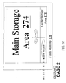
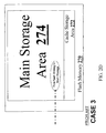
- flash memory 270 it is common in flash devices for flash memory 270 to include both a cache storage area 272 and a main storage area 274 for "longer term" storage. Incoming data may, at least some of the time, be written to the cache storage area 272 and, at a later time, be copied from cache storage area 272 to the main storage area 274.
- the cache storage area 272 is written to using a 'faster writing mode' that is faster than a writing mode used for main storage area 274 and/or the main storage area 274 is larger (i.e. has a greater capacity) than the cache storage area 272 .
- cache storage area 272 includes flash blocks where K bits of data are stored in each flash cell where K is a positive integer
- main storage area 274 includes flash blocks where L bits of data are stored in each flash cell where L is a positive integer that exceeds K .
- FIG. 2B relates to a first use case. According to this use case, data is written to the cache storage area only.
- FIG. 2C which relates to a second use case (i) data is first written to the cache storage area 272; and (ii) at a later time, the data is copied from the cache storage area 272 to the main storage area 274.
- FIG. 2D relating to a third use case, describes "cache bypassing."
- data is written directly to the main storage area 274 without first being written to the cache storage area 272.
- FIG. 3 is a flow chart describing a technique for storing data to a flash memory 270.
- the peripheral storage device 260 receives data from host device 310.
- this data is stored in volatile memory (for example within flash controller 280 or at any other location within non-volatile memory device 260 ).
- the data is either (i) written to cache storage area 272 before being written (if written) to main storage area 274 (use cases 1 and 2) - i.e. the 'first flash writing' of the data is to cache 272 or (ii) is written to main storage area 274 without being written to cache storage area 272 (use case 3) - i.e. the 'first flash writing' of the data is to the main storage area 274.
- the 'yes' branch leaving step S219 is selected, and the data is written (in step S223 ) into the cache storage area 272.
- the data is copied (see the optionally line leaving the box of step S223 ) from the typically smaller cache storage area to the larger main storage area for longer-term storage. Copying the data allows the region within cache 272 in which the data was stored to be used to store new data
- the data may be written directly to main storage area 274 (according to the 'no' branch leaving step S219 ) without writing the data first to the cache storage area
- flash controller 280 may be implemented using any combination or hardware (for example, including a microprocessor and optionally volatile memory such as RAM or registers), firmware and/or code-modules (for example, stored in volatile and/or non-volatile memory and executable by a microprocessor). Flash controller 280 may include any software (i.e. tangibly stored in volatile and/or non-volatile memory) and/or firmware and/or hardware element(s) including but not limited to field programmable logic array (FPLA) element(s), field programmable gate array (FPGA) element(s), and application-specific integrated circuit (ASIC) element(s). Any instruction set architecture may be used in flash controller 280 including but not limited to reduced instruction set computer (RISC) element(s) and/or complex instruction set computer (CISC) .
- RISC reduced instruction set computer
- CISC complex instruction set computer
- US2007/016725 discloses a method of writing data to a memory disc directly or via Flash write cache depending on whether the data is received in a bursty mode.
- US2004/117441 discloses a storage system comprising a data-aware data flow manager. If access to storage within the system is requested the data flow manager determines which data to cache and which data to send directly to the storage.
- US6,496,905 discloses a further storage system comprising a right buffer operative to buffer data to be written to the storage system.
- a method of implementing a caching policy for a non-volatile storage device that has a non-volatile memory including a cache storage area and a main storage area.
- the method comprises a) receiving data by the non-volatile storage device from a host device coupled to the non-volatile storage device, b) determining by the non-volatile storage device whether to write the received data to the cache storage area of the non-volatile memory before writing the received data to the main storage area of the non-volatile memory in accordance with at least one parameter selected from the group consisting of a historical rate at which other data was received by the non-volatile storage device from the host device during a time period preceding the receiving of the data of step (a) and an average time interval between successive host write requests received during the preceding time period and c) in the event of a positive determining, writing the data received in step (a) to the cache storage area as determined.
- the at least one parameter includes the historical rate at which the other data was received
- determining to write the received data to the cache storage area of the non-volatile memory before writing the data to the main storage area is contingent upon the historical rate being above a threshold level.
- the at least one parameter includes the average time interval between successive host write requests received during the preceding time period
- the determining to write the received data to the cache storage area of the non-volatile memory before writing the data to the main storage area is contingent upon the average time period being below a threshold level.
- the data-receiving is carried out before the determining.
- a system comprising a non-volatile storage device that has a non-volatile memory including a cache storage area and a main storage area.
- the system is configured to implement a caching policy for a non-volatile storage device, comprising a) means for receiving data by the non-volatile storage device from a host device coupled to the non-volatile storage device, b) means for determining by the non-volatile storage device whether to write the received data to the cache storage area of the non-volatile memory before writing the received data to the main storage area of the non-volatile memory in accordance with at least one parameter selected from the group consisting of a historical rate at which other data was received by the non-volatile storage device from the host device during a time period preceding the receiving of the data of step (a) and an average time interval between successive host write requests received during the preceding time period and c) means operative to write the data received in step (a) to the cache storage area as determined in the
- determining to write the received data to the cache storage area of the non-volatile memory before writing the data to the main storage area is contingent upon the historical rate being above a threshold level.
- the at least one parameter includes the average time interval between successive host write requests received during the preceding time period, the determining to write the received data to the cache storage area of the non-volatile memory before writing the data to the main storage area is contingent upon the average time period being below a threshold level.
- a method of implementing a caching policy for a non-volatile storage device that has a non-volatile memory including a cache storage area and a main storage area, the method comprising: a) receiving at least one request by the non-volatile storage device from a host device coupled to the non-volatile storage device to store data in the non- volatile memory; b) assessing a rate at which data is required to be written to the non-volatile memory in order to fulfill the at least one data storage request; c) in accordance with the assessed data-writing rate, determining whether to write the received data to the cache storage area of the non-volatile memory before writing the received data to the main storage area of the non-volatile memory; and d) in the event of a positive determining, writing the received data to the cache area as determined.
- the receiving of the at least one request may include receiving a first request and a second request; i) the rate assessing is carried out in accordance with: (A) respective amounts of data of the first and second requests; and B) a time difference between a time of receiving the first request and a time of receiving the second request.
- the receiving of the at least one request includes receiving a first request and a second request; ii) the rate assessing is carried out in accordance with a quotient between: A) the total amount of data of the first and second requests; and B) a time difference between a time of receiving the first request and a time of receiving the second request.
- a method of implementing a caching policy for a non-volatile storage device that has a non-volatile memory including a cache storage area and a main storage area, the method comprising: a) receiving a request by the non-volatile storage device from a host device coupled to the non-volatile storage device to store data in the non-volatile memory; b) if the non-volatile storage device is in a store-to-cache-first mode at a time that the request is received, write the received data to the cache storage area of the non-volatile memory before writing the received data to the main storage area of the non-volatile memory; c) if the non-volatile storage device is in a bypass-cache mode at a time that the request is received, write the received data to the main storage area of the non-volatile memory without writing the received data to the cache storage area of the non-volatile memory; and d) effecting a mode transition, by the storage device
- the method may further comprise: e) in accordance with a fullness of the cache storage area, deciding whether or not to transition from the store-to-cache-first mode to the bypass-cache mode; and f) effecting the transition from the store-to-cache-first mode to the bypass-cache mode as determined.
- a method of implementing a cache flushing policy for a non-volatile storage device comprising: a) receiving data by the non-volatile storage device from a host device coupled to the non-volatile storage device; b) storing the received data in the cache storage area; and c) for at least one point in time: i) determining, by the non-volatile storage device, in accordance with at least one parameter selected from the group consisting of: A) a historical rate at which other data was received by the non-volatile storage device from the host device during a time period preceding the receiving of the data of step (a); and B) an average time interval between successive host write requests received during the preceding time period; and whether to copy the data received in step (a) from the cache storage area of the non-volatile memory to the main storage area of the non-volatile memory; and ii) in the event
- the at least one parameter may include the average time interval between successive host write requests.
- a non-volatile storage device comprising: a) a device interface for coupling with a host device; b) a non-volatile memory including a cache storage area and a main storage area; and c) a controller operative to: i) receive data from the host device via the device interface; ii) determine whether to write the received data to the cache storage area before writing the received data to the main storage in accordance with at least one parameter selected from the group consisting of: A) a historical rate at which other data was received by the non-volatile storage device from the host device during a time period preceding the receiving of the data of step (c)(i); and B) an average time interval between successive host write requests received during the preceding time period; and iii) in the event of a positive determining, write the data received in step (c)(i) to the cache storage area as determined.
- a non-volatile storage device comprising: a) a device interface for coupling with a host device; b) a non-volatile memory including a cache storage area and a main storage area; and c) a controller operative to: i) receive, from the host device via the device interface, at least one request to store data in the non-volatile memory; ii) assess a rate at which data is required to be written to the non-volatile memory in order to fulfill the at least one data storage request; iii) in accordance with the assessed data-writing rate, determine whether to write the received data to the cache storage area before writing the received data to the main storage area; and iv) in the event of a positive determining, write the received data to the cache storage area as determined.
- a non-volatile storage device comprising: a) a device interface for coupling with a host device; b) a non-volatile memory including a cache storage area and a main storage area; and c) a controller operative to: i) receive, from the host device via the device interface, a request to store data in the non-volatile memory; ii) if the non-volatile storage device is in a store-to-cache-first mode at a time that the request is received , write the received data to the cache storage area before writing the received data to the main storage area; iii) if the non-volatile storage device is in a bypass-cache mode at a time that the request is received, write the received data to the main storage area without writing the received data to the cache storage area of the non-volatile memory; and iv) effect a mode transition, by the storage device, from the bypass-cache mode to the store-to-cache-first mode in
- a non-volatile storage device comprising: a) a device interface for coupling with a host device; b) a non-volatile memory including a cache storage area and a main storage area; and c) a controller operative to: i) receive data from the host device via the device interface; ii) store the received data in the cache storage area; and iii) for at least one point in time: A) determine in accordance with at least one parameter selected from the group consisting of: I) a historical rate at which other data was received by the non-volatile storage device from the host device during a time period preceding the receiving of the data of step (a); and II) an average time interval between successive host write requests received during the preceding time period; and whether to copy the data received in step c(i) from the cache storage area to the main storage area; and iv) in the event of a positive determining, copying the data received in step c(i) from the cache storage area as determined.
- Some embodiments of the present invention relate to utilizing certain historical and/or predicted performance data' when deciding whether: (i) to store data to a cache storage area before storing the data to a main storage area of a non-volatile memory; or (ii) to 'bypass' the cache storage area by storing the data 'directly' in the main storage area.
- the decision of whether or not to write 'incoming data' to the cache storage area may be carried out in accordance with one or more of: (i) historical rates at which data has been received by a peripheral storage device from a host device ('Parameter A') (see FIG.
- a determining of whether or when to copy 'cache-residing data' i.e. data that has already been written into the cache storage area
- a determining of whether or when to copy 'cache-residing data' may also be carried out in accordance with one or more of the aforementioned parameter(s) and/or other parameters described herein. These embodiments may be useful for determining and enforcing a 'non-volatile cache flushing' policy.
- peripheral storage device in the event that the peripheral storage device has recently been 'flooded' with a 'large' amount of data from the host device (i.e. data sent from the host device which needs to be stored in non-volatile storage within the peripheral storage device) in a 'short' period of time, then it may be assumed that there is an 'elevated' likelihood that in the near future, the rate at which data will be received will continue to be relatively 'high.' In this case, incoming data is stored first to the cache, which is associated with a 'faster writing speed,' rather than directly writing to the 'slower' main storage region. This may be useful for minimizing the risk of a slow response time (i.e. as detectable by the host) for completing the execution of one or more write commands received from the host device.
- a slow response time i.e. as detectable by the host
- the rate at which data is written from the host device is historically 'low,' it may be preferred, when receiving data from the host device, to bypass the cache storage area and to write the received data 'directly' to the main storage area. In this case, refraining from storing the data to the cache storage area may be useful, for example, for minimizing the number of write operations sustained by the cache storage area of the non-volatile (for example, flash) memory, thereby extending the lifespan of cache area and/or the peripheral non-volatile storage device.
- the non-volatile for example, flash
- the rate at which data has been historically received may be indicative of an estimated rate at which data will be received from the host device in the future.
- an average time interval between successive host write-requests received during a preceding time period may be indicative of a magnitude of a workload imposed upon the peripheral storage device by the host device during the preceding time period.
- this may be indicative of (i) a situation where the host has provided many write requests in a relatively short period of time, thereby imposing a relatively 'large' workload upon the peripheral storage device; and (ii) an elevated likelihood that the peripheral storage device will need to handle a large workload in the future.
- the average time interval is relatively low (for example, below some threshold, pre-determined or otherwise), it may be preferred to first write incoming data received from the host device to the cache storage area, in order to minimize the risk of a slow response time (i.e. as detectable by the host) for completing the execution of one or more write commands received by the host device.
- this may be indicative of (i) a host that has been relatively 'inactive' in the past; and (ii) a host which has an elevated likelihood of being inactive in the future (or a reduced likelihood of being active).
- it may be preferred, when receiving data from the host device, to bypass the cache storage area and to write the received data 'directly' to the main storage area, despite the slower writing speed.
- refraining from storing the data to the cache storage area may be useful, for example, for minimizing the number of write operations sustained by the cache storage area of the non-volatile (for example, flash) memory, thereby extending the lifespan of cache area and/or the peripheral non-volatile storage device.
- the non-volatile for example, flash
- a rate at which data received in one or more command(s) from the host is required to be written to non-volatile memory of the peripheral non-volatile memory device is assessed.
- information describing this rate may be received explicitly from the host.
- non-volatile memory when receiving data from the host device, it may be preferred, when receiving data from the host device, to bypass the cache storage area and to write the received data 'directly' to the main storage area, despite the slower writing speed. In this case, refraining from storing the data to the cache storage area may be useful, for example, for minimizing the number of write operations sustained by the cache storage area of the non-volatile (for example, flash) memory, thereby extending the lifespan of cache area and/or the peripheral non-volatile storage device.
- the non-volatile for example, flash
- the decision of whether or not to write to cache before writing to main storage may be carried out "autonomously" by a peripheral non-volatile storage device), without receiving any caching instructions from the host device.
- 'cache-residing data' i.e. data that has already been written into the cache storage area
- the data is copied from the cache storage area to the main storage area contingent upon and/or in accordance with this determining.
- the determining of whether or when to copy 'cache-residing data' from the cache storage area may be carried out in accordance with one or more of: (i) historical rates at which data has been received by a peripheral storage device from a host device ('Parameter A') (see FIG. 5 ); (ii) an average time interval between successive host write requests received during a preceding time period ('Parameter B') (see FIG. 6 ); and/or (iiii) one or more additional parameters described below.
- the rate at which data is written from the host device is historically 'low,' it may be preferred, when receiving data from the host device, to take advantage of the situation by dedicating device resources to the task of copying data from the cache storage area to the main storage area. Because it is anticipated that the demands placed upon the peripheral storage device by the host device will be relatively “low” in the near future, it may be assumed that the risk of the device failing to meet any of these demands will be relatively low during the time period where device resources are dedicated to copying data from the cache, providing an opportunity to "clear" the cache for new incoming data.
- an average time interval between successive host write-requests received during a preceding time period is indicative of how 'active' the host device has been in sending commands or specific tasks to the peripheral storage device.
- this may be indicative of (i) a situation where the host has provided many write requests in a relatively short period of time, thereby imposing a relatively 'large' workload upon the peripheral storage device; and (ii) an elevated likelihood that the peripheral storage device will need to handle a large workload in the future.
- the cache copying operations whereby data is copied from the cache storage area to the main storage area may consume device resources of the peripheral non-volatile storage device, and may limit the amount of device resources available for handling "incoming data.”
- diverting device resources to cache flushing may increase the risk that the peripheral storage device will not be able to "handle" the incoming data (i.e. as detectable by the host device) at the rate required and/or required.
- the decision of whether or not (or when) to copy 'cache-residing data' from the cache area to the main area may be carried out "autonomously" by a peripheral flash device, without receiving any caching instructions from the host device.
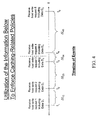
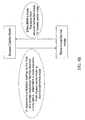
- FIG. 4 is a timeline describing information which may be utilized to enforce one or more cache-related policy(ies).
- a first "write request” including data D 1 is received at peripheral storage device 260 from host device 310 via respective interfaces 350 , 250 .
- a second "write request” including data D 2 is received at peripheral storage device 260 from host device 310 via respective interfaces 350 , 250 .
- a third "write request” including data D 3 is received at peripheral storage device 260 from host device 310 via respective interfaces 350 , 250 .
- a fourth "write request" including data D 4 is received at peripheral storage device 260 from host device 310 via respective interfaces 350 , 250 .
- a fifth "write request" including data D 5 is received at peripheral storage device 260 from host device 310 via respective interfaces 350 , 250 .
- the "time gap” between (i) the receiving of data D2 /the receiving of the second write request and (ii) the receiving of data of D1 /the receiving of the first write request is ⁇ t 12 .
- the "time gap” between (i) the receiving of data D3 //the receiving of the third write request and (ii) the receiving of data of D2 /the receiving of the second write request is ⁇ t 23 .
- the "time gap” between (i) the receiving of data D4 /the receiving of the fourth write request and (ii) the receiving of data of D3/the receiving of the third write request is ⁇ t 34 .
- the "time gap” between (i) the receiving of data D5 /the receiving of the fifth write request and (ii) the receiving of data of D4 /the receiving of the fourth write request is ⁇ t 45 .
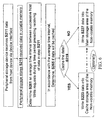
- FIG. 5 is a flow chart describing a technique for storing data to a flash memory 270 .
- the peripheral storage device 260 receives data from host device 310 .
- this data is stored in volatile memory (for example within flash controller 280 or at any other location within non-volatile memory device 260 ).
- step S251 a historical rate at which other data was received during a time period preceding the receiving of data in step S211 is assessed or determined.
- step S211 is carried out at time t 4 as part of receiving command 4.
- the "data" received is D 4 .
- the preceding time period begins at time t 2 - ⁇ t 12 and ends at time t 3 + ⁇ t 34 .
- the total "length" of the preceding time interval is ( t 3 + ⁇ t 34 ) - ( t 2 - ⁇ t 12 ), and the total amount of "other data" received during the "preceding time interval" (i.e. which preceded time t 4 ) is ( D 2 + D 3 ).
- the 'historical rate' R at which the "other data" is received during the "historical time period” is D 2 + D 3 t 3 + ⁇ ⁇ t 34 - t 2 - ⁇ ⁇ t 12 .
- step S255 it is determined in accordance with the historical data receiving rate R if the data will be cached.
- R is compared with some sort of threshold (for example, a predetermined threshold value and/or a threshold value which changes as a function of time and/or any other threshold value): (i) in the event that R exceeds the threshold, the "yes" branch leaving S219 is taken; and (ii) otherwise, the "no" branch leaving S219 is taken.
- some sort of threshold for example, a predetermined threshold value and/or a threshold value which changes as a function of time and/or any other threshold value
- FIG. 6 is a flow chart describing a technique for storing data to a flash memory 270 .
- the peripheral storage device 260 receives data from host device 310.
- this data is stored in volatile memory (for example within flash controller 280 or at any other location within non-volatile memory device 260 ).
- step S261 an average time interval between successive host write requests during a time period preceding the receiving of data in step S211 is assessed or determined.
- step S211 is carried out at time t 5 as part of receiving command 5.
- the preceding time period begins at time t 2 - ⁇ t 12 and ends at time t 4 + ⁇ t 45 .
- three host write requests are received: the second write request at time t 2 , the third write request at time t 3 , and the fourth write request at time t 4 .
- the average time interval between successive host write requests TAVC is ⁇ ⁇ t 23 + ⁇ ⁇ t 34 2 .
- step S265 it is determined in accordance with the average time interval between successive host write requests T AVG if the data will be cached.
- T AVG is compared with some sort of threshold (for example, a predetermined threshold value and/or a threshold value which changes as a function of time and/or any other threshold value): (i) in the event that T AVG is less than the threshold, the "yes" branch leaving S219 is taken; and (ii) otherwise, the "no" branch leaving S219 is taken.
- some sort of threshold for example, a predetermined threshold value and/or a threshold value which changes as a function of time and/or any other threshold value
- FIG. 7 is a flow chart describing a technique for storing data to a flash memory 270 .
- the peripheral storage device 260 receives data from host device 310 .
- this data is stored in volatile memory (for example within flash controller 280 or at any other location within non-volatile memory device 260 ).
- step S315 a rate at which data received in step S311 is required to be written to non-volatile memory to fulfill the at least one data storage request may be assessed.
- this information may be received explicitly - for example, the command set of the peripheral storage device may include a write command with a syntax where the host device requests that a certain amount of data be stored within a certain amount of time.
- the rate at which data is required to be written may then be considered to be a function of: (i) the amount of data received from the host device in the particular command; and (ii) the amount of time in which the data is to be written, according to the request from the host device.
- historical patterns may be used to estimate a rate in which data is required to be written to non-volatile memory.
- step S319 it is determined in accordance with the assessed rate AR at which data is required to be written if the data will be cached.
- AR is compared with some sort of threshold (for example, a predetermined threshold value and/or a threshold value which changes as a function of time and/or any other threshold value): (i) in the event that AR is greater than the threshold (i.e. requiring that data is witten relatively quickly), the "yes" branch leaving S219 is taken; and (ii) otherwise, the "no" branch leaving S219 is taken.
- some sort of threshold for example, a predetermined threshold value and/or a threshold value which changes as a function of time and/or any other threshold value
- FIGS. 8A-8B According to an arrangement not in accordance with the present invention and illustrated in FIGS. 8A-8B , if the host reads a storage ready/busy flag (i.e. of the peripheral storage device 260 ) that returned a busy status, this may be indicative that the peripheral storage device is not successfully writing data to non-volatile storage at the rate "desired" by the host device. In this case, in order to provide "better performance" for the host device, it may be desirable to first write incoming data to the cache storage area, utilizing the "fast writing" property provided by the cache storage area.
- a storage ready/busy flag i.e. of the peripheral storage device 260
- this may be indicative that the peripheral storage device is not successfully writing data to non-volatile storage at the rate "desired" by the host device.
- FIG. 8A is a flow chart describing a technique for storing data to a flash memory 270.
- peripheral storage device 260 provides at least two device “modes”: a first mode referred to as the "store-to-cache-first” device mode whereby data is stored in the cache storage area 272 before being written to the main storage area 274 , and a second mode referred to as “bypass-cache mode” whereby data is stored in the main storage area 274 without being written to the cache storage area 272 .
- Information about a "current mode” may be stored in any location, including but not limited to flash controller 280 , volatile memory 282 and flash memory 270 .
- step S211 of FIG. 8A the peripheral storage device 260 receives data from host device 310 .
- this data is stored in volatile memory (for example within flash controller 280 or at any other location within non-volatile memory device 260 ).
- FIG. 8B is a flow chart of routine for transitioning between the two aforementioned device modes.
- the device may transition from the "bypass cache mode" to the store-to-cache-first mode in response to a reading, by the host, of a storage ready/busy flag (i.e, the host queries the peripheral storage device of its status, and the peripheral storage device returns a storage ready/busy flag to the host device which is read by the host device).
- a storage ready/busy flag i.e, the host queries the peripheral storage device of its status, and the peripheral storage device returns a storage ready/busy flag to the host device which is read by the host device.
- peripheral storage device 260 effects a transition back to bypass cache mode in accordance with one or more events.
- this transition in accordance with a "fullness" of the cache storage area (i.e. how full the cache area is 272 with previously-written data) - for example, if the cache is close to "full” it may be advisable to effect the transition from the store-to-cache-first mode to a bypass cache mode, since there is not enough space in the cache to write incoming data into the flash.
- step S271 of FIG. 8A it is noted that: (i) in the event that peripheral device 260 is in "store-to-cache-first” mode, the "left" branch leaving step S271 is taken; and (ii) otherwise, the "right” branch leaving step S271 is taken.
- FIGS. 5-8 describe routines for implementing a policy for storing incoming data to non-volatile memory 270 of a peripheral storage device 260 .
- FIG. 9-10 describe routines for copying data from a cache storage area 270 of a non-volatile memory to a main storage area 274 (see the earlier section entitled "An Introductory Discussion of Techniques for Copying Data from a Cache Storage Area of Non-Volatile Memory of a Peripheral Non-Volatile Memory Storage Device to a Main Storage Area").
- step S511 the peripheral storage device 260 receives data from host device 310 .
- this data is stored in the cache storage area 272 of non-volatile memory 270 .
- step S519 an historical rate at which other data was received during a time period preceding the receiving of data in step S511 is determined (see step S251 of FIG. 5 ).
- step S523 it is determined, in accordance with the historical data receiving rate, if data will be copied (i.e. at a particular time or in a particular time frame or at any time) from the cache storage area 272 to the main storage area 274 .
- step S523 if step S523 yielded a "positive determining" (i.e. a determining that data will be copied from the cache storage area 272 to the main storage area 274 ), then data is copied from the cache storage area 272 to the main storage area 274 as determined.
- a "positive determining" i.e. a determining that data will be copied from the cache storage area 272 to the main storage area 274
- any of the step(s) of FIG. 9 may be repeated any number of times.
- the historical rate at which data was received may be monitored (for example, at a plurality of points in time), and in response to an increase (or decrease) of the historical rate (which itself may fluctuate in time), data may be copied from the cache storage area 272 to the main storage area 274 , or a process in which data is being copied from cache storage area 272 to the main storage area 274 may cease.
- step S511 the peripheral storage device 260 receives data from host device 310 .
- this data is stored in the cache storage area 272 of non-volatile memory 270 .
- step S519 a magnitude of an average time interval between successive host write requests sent form host 310 to peripheral storage device 260 during a historical time period preceding the receiving of data in step S511 is determined (see step S261 of FIG. 6 ).
- step S531 it is determined, in accordance with the magnitude of the average time interval, if data will be copied (i.e. at a particular time or in a particular time frame or at any time) from the cache storage area 272 to the main storage area 274 .
- step S535 if step S523 yielded a "positive determining" (i.e. a determining that data will be copied from the cache storage area 272 to the main storage area 274 ), then data is copied from the cache storage area 272 to the main storage area 274 as determined.
- a "positive determining" i.e. a determining that data will be copied from the cache storage area 272 to the main storage area 274
- any of the step(s) of FIG. 10 may be repeated any number of times.
- the average time interval between successive host write requests may be monitored (for example, at a plurality of points in time), and in response to an increase (or decrease) of the historical rate (which itself may fluctuate in time), data may be copied from the cache storage area 272 to the main storage area 274 , or a process in which data is being copied from cache storage area 272 to the main storage area 274 may cease.
- Non-volatile memory refers to any kind of non-volatile memory including flash memory and magnetic memory.
- “Incoming data” refers to data received by a flash memory device from a host that has not yet been stored in non-volatile memory (for example, flash memory) of the flash memory device. "Incoming data” may be temporarily stored (for example, by flash controller 280 ) in volatile memory 270 within the flash memory device.
- an "extend to which the cache storage area 272 is full of previously-stored data” is determined.
- "Previously-stored data” refers to data stored in cache storage area 272 of non-volatile memory 270 before the time at which the "extent to which the flash memory storage device is full of previously-stored data” is determined.
- any of the embodiments described above may further include receiving, sending or storing instructions and/or data that implement the operations described above in conjunction with the figures upon a computer readable medium.
- a computer readable medium may include storage media or memory media such as magnetic or flash or optical media, e.g, disk or CD-ROM, volatile or non-volatile media such as RAM, ROM, etc. as well as transmission media or signals such as electrical, electromagnetic or digital signals conveyed via a communication medium such as network and/or wireless links.
Landscapes
- Engineering & Computer Science (AREA)
- Theoretical Computer Science (AREA)
- Physics & Mathematics (AREA)
- General Engineering & Computer Science (AREA)
- General Physics & Mathematics (AREA)
- Human Computer Interaction (AREA)
- Memory System Of A Hierarchy Structure (AREA)
Description
- The present invention relates to techniques and apparatus for implementing a caching policy for a non-volatile memory such as a flash memory.
- Multi-Level Cell (MLC) flash memory are useful for storing more than one bit of data on each memory cell. The writing of data into an MLC flash memory is typically slower than the writing of data into a Single-Level Cell (SLC) flash memory that stores only one bit of data per cell. Therefore, flash devices based on an MLC flash memory might not be capable of recording a stream of incoming data transmitted to it at a rate that exceeds the writing rate associated with the MLC flash memory.
- Typically in cases where data is produced at a rate too high to be directly stored, a cache memory mechanism is provided and designed to operate fast enough to handle the incoming data stream. The cache memory utilizing a second (and faster) memory is implemented between the input data source and the main (and slower) memory of the flash memory device. The input data stream is first written into the faster cache memory, and at a later stage is copied from this faster cache memory into the main memory. As the copying operation between the cache memory and the main memory is typically performed in the background, this operation does not have to meet the strict performance conditions imposed by the input data stream rate, and therefore the lower write performance of the main memory is no longer an obstacle.
- One type of flash memory device is a 'peripheral flash storage device" which is now discussed with reference to
FIG. 1 . - "Peripheral flash storage devices" 260 are well-known in the art of computing, in form factors such as USB flash drives (UFD); PC-cards; and small storage cards used with digital cameras, music players, handheld and palmtop computers, cellular telephones or any other form factor.
- When coupled to a host device 310 (for example, a laptop or desktop computer or a mobile telephone), the peripheral
flash storage devices 260 may receive user data viarespective host side 350 anddevice side 250 interfaces (for example, a USB interface or an SD interface or an MMC interface or any other kind of wired or wireless interface). The received data may be written byflash controller 280 toflash memory 270 of the flash memory storage device. - Although
host 310 andflash 260 devices are illustrated inFIG. 1 as separate devices, it is understood that in some embodiments,flash device 260 may be deployed within a housing of host device. Alternatively,flash device 260 may be deployed outside of a housing of host device. - As illustrated in
FIG. 1 ,host device 310 sends data to flash memory storage device 260 (for example, associated with a write command). The data, which is received from the host, is written tovolatile memory 282, for example byflash controller 280. Althoughvolatile memory 282 is depicted inFIG. 1 as separate fromflash controller 280, it is appreciated that, in some embodiments, volatile memory 282 (for example, RAM) may reside within and/or be a part offlash controller 280, - After the data is written to
volatile memory 282, it is copied toflash memory 270. - It is noted that when the
host device 310 sends a write command to theflash device 260, there may be a need for theflash device 260 to write the data to flashmemory 270 as soon as possible in. On the other hand, as noted above, sometimes other design considerations (e.g. the need to greater device capacity and/or reliability) may require that a "slower" writing mode that is slower than the fastest possible writing mode be used. - Towards this end, as illustrated in
FIG. 2A , it is common in flash devices forflash memory 270 to include both acache storage area 272 and amain storage area 274 for "longer term" storage. Incoming data may, at least some of the time, be written to thecache storage area 272 and, at a later time, be copied fromcache storage area 272 to themain storage area 274. - In different implementations, the
cache storage area 272 is written to using a 'faster writing mode' that is faster than a writing mode used formain storage area 274 and/or themain storage area 274 is larger (i.e. has a greater capacity) than thecache storage area 272. - In one particular example,
cache storage area 272 includes flash blocks where K bits of data are stored in each flash cell where K is a positive integer, and themain storage area 274 includes flash blocks where L bits of data are stored in each flash cell where L is a positive integer that exceeds K. -
FIG. 2B relates to a first use case. According to this use case, data is written to the cache storage area only. - In the example of
FIG. 2C , which relates to a second use case (i) data is first written to thecache storage area 272; and (ii) at a later time, the data is copied from thecache storage area 272 to themain storage area 274. - The example of
FIG. 2D , relating to a third use case, describes "cache bypassing." In this third use case, data is written directly to themain storage area 274 without first being written to thecache storage area 272. -
FIG. 3 is a flow chart describing a technique for storing data to aflash memory 270. In step S211, theperipheral storage device 260 receives data fromhost device 310. In step S215, this data is stored in volatile memory (for example withinflash controller 280 or at any other location within non-volatile memory device 260). - As illustrated in the use cases described with reference to
FIGS 2B-2D , the data is either (i) written tocache storage area 272 before being written (if written) to main storage area 274 (usecases 1 and 2) - i.e. the 'first flash writing' of the data is to cache 272 or (ii) is written tomain storage area 274 without being written to cache storage area 272 (use case 3) - i.e. the 'first flash writing' of the data is to themain storage area 274. - For the former case (use
cases 1 and 2), the 'yes' branch leaving step S219 is selected, and the data is written (in step S223) into thecache storage area 272. Optionally (see use case 2) and typically with a 'high frequency' or an 'extremely high frequency,' the data is copied (see the optionally line leaving the box of step S223) from the typically smaller cache storage area to the larger main storage area for longer-term storage. Copying the data allows the region withincache 272 in which the data was stored to be used to store new data - For the latter case (use case 3) relating to 'bypassing' the cache, the data may be written directly to main storage area 274 (according to the 'no' branch leaving step S219) without writing the data first to the cache storage area
- Referring back to
FIG. 1 , it is noted thatflash controller 280 may be implemented using any combination or hardware (for example, including a microprocessor and optionally volatile memory such as RAM or registers), firmware and/or code-modules (for example, stored in volatile and/or non-volatile memory and executable by a microprocessor). Flashcontroller 280 may include any software (i.e. tangibly stored in volatile and/or non-volatile memory) and/or firmware and/or hardware element(s) including but not limited to field programmable logic array (FPLA) element(s), field programmable gate array (FPGA) element(s), and application-specific integrated circuit (ASIC) element(s). Any instruction set architecture may be used inflash controller 280 including but not limited to reduced instruction set computer (RISC) element(s) and/or complex instruction set computer (CISC) . - There is an ongoing need for method and apparatus for storing data to non-volatile memories including a cache storage area and a main storage area.
-
US2007/016725 discloses a method of writing data to a memory disc directly or via Flash write cache depending on whether the data is received in a bursty mode. -
US2004/117441 discloses a storage system comprising a data-aware data flow manager. If access to storage within the system is requested the data flow manager determines which data to cache and which data to send directly to the storage. -
US6,496,905 discloses a further storage system comprising a right buffer operative to buffer data to be written to the storage system. - According to the present invention there is provided a method of implementing a caching policy for a non-volatile storage device that has a non-volatile memory including a cache storage area and a main storage area. The method comprises a) receiving data by the non-volatile storage device from a host device coupled to the non-volatile storage device, b) determining by the non-volatile storage device whether to write the received data to the cache storage area of the non-volatile memory before writing the received data to the main storage area of the non-volatile memory in accordance with at least one parameter selected from the group consisting of a historical rate at which other data was received by the non-volatile storage device from the host device during a time period preceding the receiving of the data of step (a) and an average time interval between successive host write requests received during the preceding time period and c) in the event of a positive determining, writing the data received in step (a) to the cache storage area as determined. When the at least one parameter includes the historical rate at which the other data was received, determining to write the received data to the cache storage area of the non-volatile memory before writing the data to the main storage area is contingent upon the historical rate being above a threshold level. When the at least one parameter includes the average time interval between successive host write requests received during the preceding time period, the determining to write the received data to the cache storage area of the non-volatile memory before writing the data to the main storage area is contingent upon the average time period being below a threshold level.
- In some embodiments, the data-receiving is carried out before the determining.
- According to another aspect of the present invention there is provided a system comprising a non-volatile storage device that has a non-volatile memory including a cache storage area and a main storage area. The system is configured to implement a caching policy for a non-volatile storage device, comprising a) means for receiving data by the non-volatile storage device from a host device coupled to the non-volatile storage device, b) means for determining by the non-volatile storage device whether to write the received data to the cache storage area of the non-volatile memory before writing the received data to the main storage area of the non-volatile memory in accordance with at least one parameter selected from the group consisting of a historical rate at which other data was received by the non-volatile storage device from the host device during a time period preceding the receiving of the data of step (a) and an average time interval between successive host write requests received during the preceding time period and c) means operative to write the data received in step (a) to the cache storage area as determined in the event of a positive determining. When the at least one parameter Includes the historical rate at which the other data was received, determining to write the received data to the cache storage area of the non-volatile memory before writing the data to the main storage area is contingent upon the historical rate being above a threshold level. When the at least one parameter includes the average time interval between successive host write requests received during the preceding time period, the determining to write the received data to the cache storage area of the non-volatile memory before writing the data to the main storage area is contingent upon the average time period being below a threshold level.
- It is now disclosed for the first time a method of implementing a caching policy for a non-volatile storage device that has a non-volatile memory including a cache storage area and a main storage area, the method comprising: a) receiving at least one request by the non-volatile storage device from a host device coupled to the non-volatile storage device to store data in the non- volatile memory; b) assessing a rate at which data is required to be written to the non-volatile memory in order to fulfill the at least one data storage request; c) in accordance with the assessed data-writing rate, determining whether to write the received data to the cache storage area of the non-volatile memory before writing the received data to the main storage area of the non-volatile memory; and d) in the event of a positive determining, writing the received data to the cache area as determined.
- The receiving of the at least one request may include receiving a first request and a second request; i) the rate assessing is carried out in accordance with: (A) respective amounts of data of the first and second requests; and B) a time difference between a time of receiving the first request and a time of receiving the second request.
- In some arrangements i) the receiving of the at least one request includes receiving a first request and a second request; ii) the rate assessing is carried out in accordance with a quotient between: A) the total amount of data of the first and second requests; and B) a time difference between a time of receiving the first request and a time of receiving the second request.
- It is now disclosed for the first time a method of implementing a caching policy for a non-volatile storage device that has a non-volatile memory including a cache storage area and a main storage area, the method comprising: a) receiving a request by the non-volatile storage device from a host device coupled to the non-volatile storage device to store data in the non-volatile memory; b) if the non-volatile storage device is in a store-to-cache-first mode at a time that the request is received, write the received data to the cache storage area of the non-volatile memory before writing the received data to the main storage area of the non-volatile memory; c) if the non-volatile storage device is in a bypass-cache mode at a time that the request is received, write the received data to the main storage area of the non-volatile memory without writing the received data to the cache storage area of the non-volatile memory; and d) effecting a mode transition, by the storage device, from the bypass-cache mode to the store-to-cache-first mode in response to a detected reading, by the host, of a storage ready/busy flag that returned a busy status.
- The method may further comprise: e) in accordance with a fullness of the cache storage area, deciding whether or not to transition from the store-to-cache-first mode to the bypass-cache mode; and f) effecting the transition from the store-to-cache-first mode to the bypass-cache mode as determined.
- It is now disclosed for the first time a method of implementing a cache flushing policy for a non-volatile storage device that has a non-volatile memory including a cache storage area and a main storage area, the method comprising: a) receiving data by the non-volatile storage device from a host device coupled to the non-volatile storage device; b) storing the received data in the cache storage area; and c) for at least one point in time: i) determining, by the non-volatile storage device, in accordance with at least one parameter selected from the group consisting of: A) a historical rate at which other data was received by the non-volatile storage device from the host device during a time period preceding the receiving of the data of step (a); and B) an average time interval between successive host write requests received during the preceding time period; and whether to copy the data received in step (a) from the cache storage area of the non-volatile memory to the main storage area of the non-volatile memory; and ii) in the event of a positive determining, copying the data received in step (a) from the cache determined.
- The at least one parameter may include the average time interval between successive host write requests.
- It is now disclosed for the first time a non-volatile storage device comprising: a) a device interface for coupling with a host device; b) a non-volatile memory including a cache storage area and a main storage area; and c) a controller operative to: i) receive data from the host device via the device interface; ii) determine whether to write the received data to the cache storage area before writing the received data to the main storage in accordance with at least one parameter selected from the group consisting of: A) a historical rate at which other data was received by the non-volatile storage device from the host device during a time period preceding the receiving of the data of step (c)(i); and B) an average time interval between successive host write requests received during the preceding time period; and iii) in the event of a positive determining, write the data received in step (c)(i) to the cache storage area as determined.
- It is now disclosed for the first time a non-volatile storage device comprising: a) a device interface for coupling with a host device; b) a non-volatile memory including a cache storage area and a main storage area; and c) a controller operative to: i) receive, from the host device via the device interface, at least one request to store data in the non-volatile memory; ii) assess a rate at which data is required to be written to the non-volatile memory in order to fulfill the at least one data storage request; iii) in accordance with the assessed data-writing rate, determine whether to write the received data to the cache storage area before writing the received data to the main storage area; and iv) in the event of a positive determining, write the received data to the cache storage area as determined.
- It is now disclosed for the first time a non-volatile storage device comprising: a) a device interface for coupling with a host device; b) a non-volatile memory including a cache storage area and a main storage area; and c) a controller operative to: i) receive, from the host device via the device interface, a request to store data in the non-volatile memory; ii) if the non-volatile storage device is in a store-to-cache-first mode at a time that the request is received , write the received data to the cache storage area before writing the received data to the main storage area; iii) if the non-volatile storage device is in a bypass-cache mode at a time that the request is received, write the received data to the main storage area without writing the received data to the cache storage area of the non-volatile memory; and iv) effect a mode transition, by the storage device, from the bypass-cache mode to the store-to-cache-first mode in response to a detected reading, by the host, of a storage ready/busy flag that returned a busy status.
- It is now disclosed for the first time a non-volatile storage device comprising: a) a device interface for coupling with a host device; b) a non-volatile memory including a cache storage area and a main storage area; and c) a controller operative to: i) receive data from the host device via the device interface; ii) store the received data in the cache storage area; and iii) for at least one point in time: A) determine in accordance with at least one parameter selected from the group consisting of: I) a historical rate at which other data was received by the non-volatile storage device from the host device during a time period preceding the receiving of the data of step (a); and II) an average time interval between successive host write requests received during the preceding time period; and whether to copy the data received in step c(i) from the cache storage area to the main storage area; and iv) in the event of a positive determining, copying the data received in step c(i) from the cache storage area as determined.
- It is noted that features described above as pertaining to certain embodiments may also be included in other embodiments, unless indicated to the contrary herein below.
-
FIG. 1 is a block diagram of a prior art peripheral storage device coupled to a host device. -
FIGS. 2A-2D ,3 describe prior art routines for storing data to a non-volatile memory of a peripheral storage device. -
FIG. 4 is a timeline describing information which may be utilized to enforce one or more cache-related policy(ies). -
FIGS. 5-7 , and8A are flow charts of routines for storing data to a non-volatile memory including a cache storage area and a main storage area. -
FIG. 8B is a flow chart of a routine for transitioning between a bypass cache mode and a store-to-cache-first mode. -
FIGS. 9-10 are flow charts of routines for enforcing a cache flushing policy. - The claims below will be better understood by referring to the present detailed description of example embodiments with reference to the figures. The description, embodiments and figures are not to be taken as limiting the scope of the claims. It should be understood that not every feature of the presently disclosed methods and apparatuses is necessary in every implementation. It should also be understood that throughout this disclosure, where a process or method is shown or described, the steps of the method may be performed in any order or simultaneously, unless it is clear from the context that one step depends on another being performed first. As used throughout this application, the word "may" is used in a permissive sense (i.e., meaning "having the potential to'), rather than the mandatory sense (i.e. meaning "must").
- Some embodiments of the present invention relate to utilizing certain historical and/or predicted performance data' when deciding whether: (i) to store data to a cache storage area before storing the data to a main storage area of a non-volatile memory; or (ii) to 'bypass' the cache storage area by storing the data 'directly' in the main storage area. In particular embodiments, the decision of whether or not to write 'incoming data' to the cache storage area may be carried out in accordance with one or more of: (i) historical rates at which data has been received by a peripheral storage device from a host device ('Parameter A') (see
FIG. 5 ); (ii) an average time interval between successive host write requires received during a preceding time period ('Parameter B') (seeFIG. 6 ); (iii) (in an arrangement not in conformity with the present invention) an assessed data-writing rate at which data is required to be written to non-volatile memory in order to fulfill at least one data storage request ('Parameter C') (seeFIG. 7 ); and/or (iv) one or more additional parameters described below. In the event of a 'positive' decision (i.e. a decision to store the data to the cache storage area of the non-volatile memory), then the data is stored to the cache storage area as determined. - Furthermore, in some embodiments, a determining of whether or when to copy 'cache-residing data' (i.e. data that has already been written into the cache storage area) from the cache storage area to the main storage area may also be carried out in accordance with one or more of the aforementioned parameter(s) and/or other parameters described herein. These embodiments may be useful for determining and enforcing a 'non-volatile cache flushing' policy.
- An Introductory Discussion of Techniques for Writing Data to a Cache Storage Area and/or Main Storage Area of a Peripheral Non-Volatile Memory Storage Device
- In one non-limiting example related to "parameter A" and
FIG. 5 , in the event that the peripheral storage device has recently been 'flooded' with a 'large' amount of data from the host device (i.e. data sent from the host device which needs to be stored in non-volatile storage within the peripheral storage device) in a 'short' period of time, then it may be assumed that there is an 'elevated' likelihood that in the near future, the rate at which data will be received will continue to be relatively 'high.' In this case, incoming data is stored first to the cache, which is associated with a 'faster writing speed,' rather than directly writing to the 'slower' main storage region. This may be useful for minimizing the risk of a slow response time (i.e. as detectable by the host) for completing the execution of one or more write commands received from the host device. - Conversely, if, historically, the rate at which data is written from the host device is historically 'low,' it may be preferred, when receiving data from the host device, to bypass the cache storage area and to write the received data 'directly' to the main storage area. In this case, refraining from storing the data to the cache storage area may be useful, for example, for minimizing the number of write operations sustained by the cache storage area of the non-volatile (for example, flash) memory, thereby extending the lifespan of cache area and/or the peripheral non-volatile storage device.
- Thus, in this particular example, the rate at which data has been historically received may be indicative of an estimated rate at which data will be received from the host device in the future.
- In one non-limiting example related to "parameter B" and
FIG. 6 , an average time interval between successive host write-requests received during a preceding time period ('Parameter B') may be indicative of a magnitude of a workload imposed upon the peripheral storage device by the host device during the preceding time period. In the event that the average time interval between successive host write-requests has been relatively 'small,' this may be indicative of (i) a situation where the host has provided many write requests in a relatively short period of time, thereby imposing a relatively 'large' workload upon the peripheral storage device; and (ii) an elevated likelihood that the peripheral storage device will need to handle a large workload in the future. In this case, if the average time interval is relatively low (for example, below some threshold, pre-determined or otherwise), it may be preferred to first write incoming data received from the host device to the cache storage area, in order to minimize the risk of a slow response time (i.e. as detectable by the host) for completing the execution of one or more write commands received by the host device. - Conversely, if, historically, the average time between successive write requests is relatively 'large,' this may be indicative of (i) a host that has been relatively 'inactive' in the past; and (ii) a host which has an elevated likelihood of being inactive in the future (or a reduced likelihood of being active). In this case, it may be preferred, when receiving data from the host device, to bypass the cache storage area and to write the received data 'directly' to the main storage area, despite the slower writing speed. In this case, refraining from storing the data to the cache storage area may be useful, for example, for minimizing the number of write operations sustained by the cache storage area of the non-volatile (for example, flash) memory, thereby extending the lifespan of cache area and/or the peripheral non-volatile storage device.
- In one arrangement not in accordance with the present invention related to "parameter C" and
FIG. 7 , a rate at which data received in one or more command(s) from the host is required to be written to non-volatile memory of the peripheral non-volatile memory device is assessed. In one non-limiting example, information describing this rate may be received explicitly from the host. In the event that the device is required to write the data "very quickly," then it may be advantageous, in order to provide the required performance, to first write incoming data received from the host device to the cache storage area (which is associated with relatively "fast" writing), in order to meet the assessed writing rate requirements. - Conversely, if only a relatively "low rate" of data-storage to non-volatile memory is required, it may be preferred, when receiving data from the host device, to bypass the cache storage area and to write the received data 'directly' to the main storage area, despite the slower writing speed. In this case, refraining from storing the data to the cache storage area may be useful, for example, for minimizing the number of write operations sustained by the cache storage area of the non-volatile (for example, flash) memory, thereby extending the lifespan of cache area and/or the peripheral non-volatile storage device.
- It is noted that in different embodiments, the decision of whether or not to write to cache before writing to main storage may be carried out "autonomously" by a peripheral non-volatile storage device), without receiving any caching instructions from the host device.
- An Introductory Discussion of Techniques for Copying Data from a Cache Storage Area of Non-Volatile Memory of Peripheral Non-Volatile memory Storage Device to a Main
- As noted earlier, also disclosed is a technique for determining whether or when to copy 'cache-residing data' (i.e. data that has already been written into the cache storage area) from the cache storage area to the main storage area. The data is copied from the cache storage area to the main storage area contingent upon and/or in accordance with this determining.
- In some embodiments, the determining of whether or when to copy 'cache-residing data' from the cache storage area may be carried out in accordance with one or more of: (i) historical rates at which data has been received by a peripheral storage device from a host device ('Parameter A') (see
FIG. 5 ); (ii) an average time interval between successive host write requests received during a preceding time period ('Parameter B') (seeFIG. 6 ); and/or (iiii) one or more additional parameters described below. - In one arrangement not in accordance with the present invention related to "parameter A" and
FIG. 9 , in the event that the peripheral storage device has recently been 'flooded' with a 'large' amount of data from the host device (i.e. data sent from the host device which needs to be stored in non-volatile storage within the peripheral storage device) in a 'short' period of time, then it may be assumed that there is an 'elevated' likelihood that in the near future the rate at which data will be received will continue to be relatively 'high.' In this case, it may be advantageous to postpone flushing the cache (postpone copying data from the cache storage area to the main storage area) and/or flush the cache at a relatively 'low rate.' In particular, the cache copying operations whereby data is copied from the cache storage area to the main storage area may consume device resources of the peripheral non-volatile storage device, and may limit the amount of device resources available for handling "incoming data." Thus, in the event that it is predicted that the storage device will be relatively "flooded" with new incoming data, diverting device resources to cache flushing may increase the risk that the peripheral storage device will not be able to "handle" the incoming data (i.e. as detectable by the host device) at the rate required and/or required. - Conversely, if, historically, the rate at which data is written from the host device is historically 'low,' it may be preferred, when receiving data from the host device, to take advantage of the situation by dedicating device resources to the task of copying data from the cache storage area to the main storage area. Because it is anticipated that the demands placed upon the peripheral storage device by the host device will be relatively "low" in the near future, it may be assumed that the risk of the device failing to meet any of these demands will be relatively low during the time period where device resources are dedicated to copying data from the cache, providing an opportunity to "clear" the cache for new incoming data.
- In one arrangement not in accordance with the present invention related to "parameter B" and
FIG. 10 , an average time interval between successive host write-requests received during a preceding time period ('Parameter B') is indicative of how 'active' the host device has been in sending commands or specific tasks to the peripheral storage device. In the event that the average time interval between successive host write-requests has been relatively 'small,' this may be indicative of (i) a situation where the host has provided many write requests in a relatively short period of time, thereby imposing a relatively 'large' workload upon the peripheral storage device; and (ii) an elevated likelihood that the peripheral storage device will need to handle a large workload in the future. In this case, if the average time interval is relatively low (for example, below some threshold, pre-determined or otherwise), it may be advantageous to postpone flushing the cache (postpone copying data from the cache storage area to the main storage area) and/or flush the cache at a relatively 'low rate.' In particular, the cache copying operations whereby data is copied from the cache storage area to the main storage area may consume device resources of the peripheral non-volatile storage device, and may limit the amount of device resources available for handling "incoming data." Thus, in the event that it is predicted (i.e. according to the average time interval between successive host write-requests received during a preceding time) that the storage device will need to handle a relatively 'large' workload, then diverting device resources to cache flushing may increase the risk that the peripheral storage device will not be able to "handle" the incoming data (i.e. as detectable by the host device) at the rate required and/or required. - Conversely, if, historically, the average time between successive write requests is relatively 'large,' this may be indicative of (i) a host that has been relatively 'inactive' in the past; and (ii) a host which has an elevated likelihood of being inactive in the future (or a reduced likelihood of being active). In this case, it may be preferred, to take advantage of the situation by dedicating device resources to the task of copying data from the cache storage area to the main storage area. Because it is anticipated that the demands placed upon the peripheral storage device by the host device will be relatively "low" in the near future, it may be assumed that the risk of the device failing to meet any of these demands will be relatively low during the time period where device resources are dedicated to copying data from the cache, providing an opportunity to "clear" the cache for new incoming data.
- It is noted that in different embodiments, the decision of whether or not (or when) to copy 'cache-residing data' from the cache area to the main area may be carried out "autonomously" by a peripheral flash device, without receiving any caching instructions from the host device.
-
FIG. 4 is a timeline describing information which may be utilized to enforce one or more cache-related policy(ies). - At time t1 , a first "write request" including data D1 is received at
peripheral storage device 260 fromhost device 310 viarespective interfaces peripheral storage device 260 fromhost device 310 viarespective interfaces peripheral storage device 260 fromhost device 310 viarespective interfaces peripheral storage device 260 fromhost device 310 viarespective interfaces peripheral storage device 260 fromhost device 310 viarespective interfaces - The "time gap" between (i) the receiving of data D2/the receiving of the second write request and (ii) the receiving of data of D1/the receiving of the first write request is Δt 12. The "time gap" between (i) the receiving of data D3//the receiving of the third write request and (ii) the receiving of data of D2/the receiving of the second write request is Δt 23. The "time gap" between (i) the receiving of data D4/the receiving of the fourth write request and (ii) the receiving of data of D3/the receiving of the third write request is Δt 34. The "time gap" between (i) the receiving of data D5/the receiving of the fifth write request and (ii) the receiving of data of D4/the receiving of the fourth write request is Δt 45.
-
FIG. 5 is a flow chart describing a technique for storing data to aflash memory 270. In step S211, theperipheral storage device 260 receives data fromhost device 310. In step S215, this data is stored in volatile memory (for example withinflash controller 280 or at any other location within non-volatile memory device 260). - In step S251, a historical rate at which other data was received during a time period preceding the receiving of data in step S211 is assessed or determined.
- Reference is made to both
FIG. 4 andFIG. 5 . In one example, step S211 is carried out at time t 4 as part of receiving command 4. In this example, the "data" received is D4 . In this example, the preceding time period begins at time t 2 - Δt 12 and ends at time t3 + Δt 34. Thus, the total "length" of the preceding time interval is (t 3 + Δt 34) - (t 2 - Δt 12), and the total amount of "other data" received during the "preceding time interval" (i.e. which preceded time t4 ) is (D2 + D3 ). Thus, in this example, the 'historical rate' R at which the "other data" is received during the "historical time period" is
- In step S255, it is determined in accordance with the historical data receiving rate R if the data will be cached. In one non-limiting example, R is compared with some sort of threshold (for example, a predetermined threshold value and/or a threshold value which changes as a function of time and/or any other threshold value): (i) in the event that R exceeds the threshold, the "yes" branch leaving S219 is taken; and (ii) otherwise, the "no" branch leaving S219 is taken.
- In the former case, data is written to the cache storage area of the
non-volatile memory 272 before being written (if at all) to themain storage area 274. For the latter "cache-bypass" case, data is written to the main storage area of thenon-volatile memory 274 without being written to thecache storage area 272. -
FIG. 6 is a flow chart describing a technique for storing data to aflash memory 270. In step S211, theperipheral storage device 260 receives data fromhost device 310. In step S215, this data is stored in volatile memory (for example withinflash controller 280 or at any other location within non-volatile memory device 260). - In step S261, an average time interval between successive host write requests during a time period preceding the receiving of data in step S211 is assessed or determined.
- Reference is made to both
FIG. 4 andFIG. 6 . In one example, step S211 is carried out at time t5 as part of receiving command 5. In this example, the preceding time period begins at time t2 - Δt 12 and ends at time t 4 + Δt 45. During this preceeding time period, three host write requests are received: the second write request at time t2 , the third write request at time t3 , and the fourth write request at time t4 . During this time interval, there are two "time intervals between successive host write requests" : Δt 23 and Δt 34, Thus, in this non-limiting example, the average time interval between successive host write requests TAVC is
- In step S265, it is determined in accordance with the average time interval between successive host write requests TAVG if the data will be cached. In one non-limiting example, TAVG is compared with some sort of threshold (for example, a predetermined threshold value and/or a threshold value which changes as a function of time and/or any other threshold value): (i) in the event that TAVG is less than the threshold, the "yes" branch leaving S219 is taken; and (ii) otherwise, the "no" branch leaving S219 is taken.
- In the former case, data is written to the cache storage area of the
non-volatile memory 272 before being written (if at all) to themain storage area 274. For the latter "cache-bypass" case, data is written to the main storage area of thenon-volatile memory 274 without being written to thecache storage area 272. -
FIG. 7 is a flow chart describing a technique for storing data to aflash memory 270. In step S311, theperipheral storage device 260 receives data fromhost device 310. In step S315, this data is stored in volatile memory (for example withinflash controller 280 or at any other location within non-volatile memory device 260). - In step S315 a rate at which data received in step S311 is required to be written to non-volatile memory to fulfill the at least one data storage request may be assessed. In one non-limiting example, this information may be received explicitly - for example, the command set of the peripheral storage device may include a write command with a syntax where the host device requests that a certain amount of data be stored within a certain amount of time. The rate at which data is required to be written may then be considered to be a function of: (i) the amount of data received from the host device in the particular command; and (ii) the amount of time in which the data is to be written, according to the request from the host device.
- In yet another example, historical patterns may be used to estimate a rate in which data is required to be written to non-volatile memory.
- In step S319, it is determined in accordance with the assessed rate AR at which data is required to be written if the data will be cached. In one non-limiting example, AR is compared with some sort of threshold (for example, a predetermined threshold value and/or a threshold value which changes as a function of time and/or any other threshold value): (i) in the event that AR is greater than the threshold (i.e. requiring that data is witten relatively quickly), the "yes" branch leaving S219 is taken; and (ii) otherwise, the "no" branch leaving S219 is taken.
- In the former case, data is written to the cache storage area of the
non-volatile memory 272 before being written (if at all) to themain storage area 274. For the latter "cache-bypass" case, data is written to the main storage area of thenon-volatile memory 274 without being written to thecache storage area 272. - Reference is made to
FIGS. 8A-8B . According to an arrangement not in accordance with the present invention and illustrated inFIGS. 8A-8B , if the host reads a storage ready/busy flag (i.e. of the peripheral storage device 260) that returned a busy status, this may be indicative that the peripheral storage device is not successfully writing data to non-volatile storage at the rate "desired" by the host device. In this case, in order to provide "better performance" for the host device, it may be desirable to first write incoming data to the cache storage area, utilizing the "fast writing" property provided by the cache storage area. -
FIG. 8A is a flow chart describing a technique for storing data to aflash memory 270. According toFIG. 8A ,peripheral storage device 260 provides at least two device "modes": a first mode referred to as the "store-to-cache-first" device mode whereby data is stored in thecache storage area 272 before being written to themain storage area 274, and a second mode referred to as "bypass-cache mode" whereby data is stored in themain storage area 274 without being written to thecache storage area 272. Information about a "current mode" may be stored in any location, including but not limited toflash controller 280,volatile memory 282 andflash memory 270. - In step S211 of
FIG. 8A , theperipheral storage device 260 receives data fromhost device 310. In step S215, this data is stored in volatile memory (for example withinflash controller 280 or at any other location within non-volatile memory device 260). -
FIG. 8B is a flow chart of routine for transitioning between the two aforementioned device modes. Thus, in step S411, the device may transition from the "bypass cache mode" to the store-to-cache-first mode in response to a reading, by the host, of a storage ready/busy flag (i.e, the host queries the peripheral storage device of its status, and the peripheral storage device returns a storage ready/busy flag to the host device which is read by the host device). This indicates both that the host device has received information that the peripheral storage device is "busy" and that it may be advantageous to use a "faster writing mode" in order to maximize performance provided to the host device. - In step S415,
peripheral storage device 260 effects a transition back to bypass cache mode in accordance with one or more events. In one non-limiting example, this transition in accordance with a "fullness" of the cache storage area (i.e. how full the cache area is 272 with previously-written data) - for example, if the cache is close to "full" it may be advisable to effect the transition from the store-to-cache-first mode to a bypass cache mode, since there is not enough space in the cache to write incoming data into the flash. - Referring now to step S271 of
FIG. 8A , it is noted that: (i) in the event thatperipheral device 260 is in "store-to-cache-first" mode, the "left" branch leaving step S271 is taken; and (ii) otherwise, the "right" branch leaving step S271 is taken. - In the former case, data is written to the cache storage area of the
non-volatile memory 272 before being written (if at all) to themain storage area 274. For the latter "cache-bypass" case, data is written to the main storage area of thenon-volatile memory 274 without being written to thecache storage area 272. -
FIGS. 5-8 describe routines for implementing a policy for storing incoming data tonon-volatile memory 270 of aperipheral storage device 260. -
FIG. 9-10 describe routines for copying data from acache storage area 270 of a non-volatile memory to a main storage area 274 (see the earlier section entitled "An Introductory Discussion of Techniques for Copying Data from a Cache Storage Area of Non-Volatile Memory of a Peripheral Non-Volatile Memory Storage Device to a Main Storage Area"). - Thus, in step S511, the
peripheral storage device 260 receives data fromhost device 310. In step S515, this data is stored in thecache storage area 272 ofnon-volatile memory 270. In step S519, an historical rate at which other data was received during a time period preceding the receiving of data in step S511 is determined (see step S251 ofFIG. 5 ). - In step S523, it is determined, in accordance with the historical data receiving rate, if data will be copied (i.e. at a particular time or in a particular time frame or at any time) from the
cache storage area 272 to themain storage area 274. In one example: (i) in the event that the historical rate at which data is received fromhost 310 is relatively "low," it may be assumed that this is indicative that the device will receive data at a "relatively low" rate in the near-future, and that device resources may be allocated to data copying from thecache storage area 272 to themain storage area 274; (ii) conversely, in the event that the historical rate at which data is received fromhost 310 is relatively "high," it may be assumed that this is indicative that the device will receive data at a "relatively high" rate in the near future, and that it is preferable to postpone copying of data from thecache storage area 272 to the main storage area - In step S523, if step S523 yielded a "positive determining" (i.e. a determining that data will be copied from the
cache storage area 272 to the main storage area 274), then data is copied from thecache storage area 272 to themain storage area 274 as determined. - It is noted that any of the step(s) of
FIG. 9 may be repeated any number of times. Thus, in one non-limiting example, the historical rate at which data was received may be monitored (for example, at a plurality of points in time), and in response to an increase (or decrease) of the historical rate (which itself may fluctuate in time), data may be copied from thecache storage area 272 to themain storage area 274, or a process in which data is being copied fromcache storage area 272 to themain storage area 274 may cease. - Reference is now made to
FIG. 10 . In step S511, theperipheral storage device 260 receives data fromhost device 310. In step S515, this data is stored in thecache storage area 272 ofnon-volatile memory 270. In step S519, a magnitude of an average time interval between successive host write requests sentform host 310 toperipheral storage device 260 during a historical time period preceding the receiving of data in step S511 is determined (see step S261 ofFIG. 6 ). - In step S531, it is determined, in accordance with the magnitude of the average time interval, if data will be copied (i.e. at a particular time or in a particular time frame or at any time) from the
cache storage area 272 to themain storage area 274. In one example: (i) in the event that the average time interval between successive write requests is relatively "large," it may be assumed that write commands will be received byperipheral device 260 fromhost 310 relatively "infrequently" in the near future and that device resources may be allocated to data copying from thecache storage area 272 to themain storage area 274; (ii) conversely, in the event the average time interval between successive write requests is relatively "small," it may be assumed that write commands will be received byperipheral device 260 fromhost 310 relatively "frequently" in the near future, thatperipheral device 260 will be relatively "busy" in the near future, and that it is preferable to postpone copying of data from thecache storage area 272 to the main storage area. - In step S535, if step S523 yielded a "positive determining" (i.e. a determining that data will be copied from the
cache storage area 272 to the main storage area 274), then data is copied from thecache storage area 272 to themain storage area 274 as determined. - It is noted that any of the step(s) of
FIG. 10 may be repeated any number of times. Thus, in one non-limiting example, the average time interval between successive host write requests may be monitored (for example, at a plurality of points in time), and in response to an increase (or decrease) of the historical rate (which itself may fluctuate in time), data may be copied from thecache storage area 272 to themain storage area 274, or a process in which data is being copied fromcache storage area 272 to themain storage area 274 may cease. - For convenience, in the context of the description herein, various terms are presented here. To the extent that definitions are provided, explicitly or implicitly, here or elsewhere in this application, such definitions are understood to be consistent with the usage of the defined terms by those of skill in the pertinent art(s). Furthermore, such definitions are to be construed in the broadest possible sense consistent with such usage.
- "Non-volatile memory" refers to any kind of non-volatile memory including flash memory and magnetic memory.
- "Incoming data" refers to data received by a flash memory device from a host that has not yet been stored in non-volatile memory (for example, flash memory) of the flash memory device. "Incoming data" may be temporarily stored (for example, by flash controller 280) in
volatile memory 270 within the flash memory device. - In some arrangements (for example related to step S415 of
FIG. 8B ), an "extend to which thecache storage area 272 is full of previously-stored data" is determined. "Previously-stored data" refers to data stored incache storage area 272 ofnon-volatile memory 270 before the time at which the "extent to which the flash memory storage device is full of previously-stored data" is determined. - It is further noted that any of the embodiments described above may further include receiving, sending or storing instructions and/or data that implement the operations described above in conjunction with the figures upon a computer readable medium. Generally speaking, a computer readable medium may include storage media or memory media such as magnetic or flash or optical media, e.g, disk or CD-ROM, volatile or non-volatile media such as RAM, ROM, etc. as well as transmission media or signals such as electrical, electromagnetic or digital signals conveyed via a communication medium such as network and/or wireless links.
- Having thus described the foregoing exemplary embodiments it will be apparent to those skilled in the art that various equivalents, alterations, modifications, and improvements thereof are possible without departing from the scope and spirit of the claims as hereafter recited. In particular, different embodiments may include combinations of features other than those described herein. Accordingly, the claims are not limited to the foregoing discussion.
Claims (4)
- A method of implementing a caching policy for a non-volatile storage device (260) that has a non-volatile memory (270) including a cache storage area (272) and a main storage area (274), the method comprising:a) receiving data by the non-volatile storage device (260) from a host
device (310) coupled to the non-volatile storage device (260);b) determining by the non-volatile storage device (260) whether to write the received data to the cache storage area (272) of the non-volatile memory (270) before writing the received data to the main storage area (274) of the non-volatile memory (270) in accordance with at least one parameter selected from the group consisting of:i) a historical rate at which other data was received by the non-volatile storage device (260) from the host device (310) during a time period preceding the receiving of the data of step (a); andii) an average time interval between successive host write requests received during the preceding time period; andc) in the event of a positive determining, writing the data received in step (a) to the cache storage area (272) as determined;
CHARACTERISED IN THAT:when the at least one parameter includes the historical rate at which the other data was received, determining to write the received data to the cache storage area (272) of the non-volatile memory (270) before writing the data to the main storage area (274) is contingent upon the historical rate being above a first threshold level; andwhen the at least one parameter includes the average time interval between the successive host write requests received during the preceding time period, the determining
to write the received data to the cache storage area (272) of the non-volatile memory (270) before writing the data to the main storage area (274) is contingent upon the average time period being below a second threshold level. - The method of claim 1 wherein the data-receiving is carried out before the determining.
- A system comprising a non-volatile storage device (260) that has a non-volatile memory (270) including a cache storage area (272) and a main storage area (274), the system being configured to implement a caching policy for a non-volatile storage device (260), and comprising:a) means for receiving data by the non-volatile storage device (260) from a host device (310) coupled to the non-volatile storage device (260);b) means for determining by the non-volatile storage device (260) whether to write the received data to the cache storage area (272) of the non-volatile memory (270) before writing the received data to the main storage area (274) of the non-volatile memory (270) in accordance with at least one parameter selected from the group consisting of:i) a historical rate at which other data was received by the non-volatile storage device (260) from the host device (310) during a time period preceding the receiving of the data of step (a); andii) an average time interval between successive host write requests received during the preceding time period; andc) means operative to write the data received in step (a) to the cache storage area (272) as determined in the event of a positive determining;
CHARACTERISED IN THAT:when the at least one parameter includes the historical rate at which the other data was received, determining to write the received data to the cache storage area (272) of the non-volatile memory (270) before writing the data to the main storage area (274) is contingent upon the historical rate being above a first threshold level; andwhen the at least one parameter includes the average time interval between the successive host write requests received during the preceding time period, the determining
to write the received data to the cache storage area (272) of the non-volatile memory (270) before writing the data to the main storage area (274) is contingent upon the average time period being below a second threshold level. - The system of claim 3 wherein the data-receiving is carried out before the determining.
Applications Claiming Priority (2)
| Application Number | Priority Date | Filing Date | Title |
|---|---|---|---|
| US12/430,089 US8103822B2 (en) | 2009-04-26 | 2009-04-26 | Method and apparatus for implementing a caching policy for non-volatile memory |
| PCT/IB2010/000858 WO2010125436A1 (en) | 2009-04-26 | 2010-04-17 | Method and apparatus for implementing a caching policy for non-volatile memory |
Publications (2)
| Publication Number | Publication Date |
|---|---|
| EP2425345A1 EP2425345A1 (en) | 2012-03-07 |
| EP2425345B1 true EP2425345B1 (en) | 2013-10-23 |
Family
ID=42288835
Family Applications (1)
| Application Number | Title | Priority Date | Filing Date |
|---|---|---|---|
| EP10717755.2A Not-in-force EP2425345B1 (en) | 2009-04-26 | 2010-04-17 | Method and apparatus for implementing a caching policy for non-volatile memory |
Country Status (6)
| Country | Link |
|---|---|
| US (1) | US8103822B2 (en) |
| EP (1) | EP2425345B1 (en) |
| JP (1) | JP2012524952A (en) |
| KR (1) | KR101201922B1 (en) |
| TW (1) | TW201109919A (en) |
| WO (1) | WO2010125436A1 (en) |
Families Citing this family (54)
| Publication number | Priority date | Publication date | Assignee | Title |
|---|---|---|---|---|
| CN104731981B (en) | 2008-09-19 | 2018-03-20 | 甲骨文国际公司 | The storage request management of memory end |
| US8868831B2 (en) | 2009-09-14 | 2014-10-21 | Oracle International Corporation | Caching data between a database server and a storage system |
| US10430338B2 (en) * | 2008-09-19 | 2019-10-01 | Oracle International Corporation | Selectively reading data from cache and primary storage based on whether cache is overloaded |
| US8499120B2 (en) * | 2008-10-17 | 2013-07-30 | Seagate Technology Llc | User selectable caching management |
| US8566531B2 (en) | 2009-08-21 | 2013-10-22 | Google Inc. | System and method of selectively caching information based on the interarrival time of requests for the same information |
| KR20110019891A (en) * | 2009-08-21 | 2011-03-02 | 삼성전자주식회사 | Remote data backup method and remote data backup system using the same |
| WO2011112523A2 (en) * | 2010-03-08 | 2011-09-15 | Hewlett-Packard Development Company, L.P. | Data storage apparatus and methods |
| JP5434738B2 (en) * | 2010-03-26 | 2014-03-05 | 日本電気株式会社 | Disk unit |
| US8402226B1 (en) * | 2010-06-18 | 2013-03-19 | Emc Corporation | Rate proportional cache write-back in a storage server |
| US8639887B2 (en) * | 2010-06-23 | 2014-01-28 | International Business Machines Corporation | Dynamically altering a pipeline controller mode based on resource availability |
| US8635409B2 (en) | 2010-06-23 | 2014-01-21 | International Business Machines Corporation | Dynamic mode transitions for cache instructions |
| US9213628B2 (en) | 2010-07-14 | 2015-12-15 | Nimble Storage, Inc. | Methods and systems for reducing churn in flash-based cache |
| US9977732B1 (en) * | 2011-01-04 | 2018-05-22 | Seagate Technology Llc | Selective nonvolatile data caching based on estimated resource usage |
| US8630418B2 (en) | 2011-01-05 | 2014-01-14 | International Business Machines Corporation | Secure management of keys in a key repository |
| US8788742B2 (en) * | 2011-05-23 | 2014-07-22 | International Business Machines Corporation | Using an attribute of a write request to determine where to cache data in a storage system having multiple caches including non-volatile storage cache in a sequential access storage device |
| US8984225B2 (en) * | 2011-06-22 | 2015-03-17 | Avago Technologies General Ip (Singapore) Pte. Ltd. | Method to improve the performance of a read ahead cache process in a storage array |
| CN107608910B (en) * | 2011-09-30 | 2021-07-02 | 英特尔公司 | Apparatus and method for implementing a multi-level memory hierarchy with different operating modes |
| US10592416B2 (en) | 2011-09-30 | 2020-03-17 | Oracle International Corporation | Write-back storage cache based on fast persistent memory |
| JP2013090006A (en) * | 2011-10-13 | 2013-05-13 | Nikon Corp | Electronic apparatus and program |
| US10681394B2 (en) | 2011-11-28 | 2020-06-09 | Comcast Cable Communications, Llc | Cache eviction during off-peak transaction time period |
| US20130151755A1 (en) | 2011-12-12 | 2013-06-13 | Reuven Elhamias | Non-Volatile Storage Systems with Go To Sleep Adaption |
| US10359972B2 (en) * | 2012-08-31 | 2019-07-23 | Sandisk Technologies Llc | Systems, methods, and interfaces for adaptive persistence |
| US10073656B2 (en) | 2012-01-27 | 2018-09-11 | Sandisk Technologies Llc | Systems and methods for storage virtualization |
| US9659041B2 (en) * | 2012-01-30 | 2017-05-23 | Oracle International Corporation | Model for capturing audit trail data with reduced probability of loss of critical data |
| US8996818B2 (en) * | 2012-12-09 | 2015-03-31 | Advanced Micro Devices, Inc. | Bypassing memory requests to a main memory |
| US9058282B2 (en) | 2012-12-31 | 2015-06-16 | Intel Corporation | Dynamic cache write policy |
| US9170943B2 (en) * | 2013-08-29 | 2015-10-27 | Globalfoundries U.S. 2 Llc | Selectively enabling write caching in a storage system based on performance metrics |
| US10229161B2 (en) | 2013-09-20 | 2019-03-12 | Oracle International Corporation | Automatic caching of scan and random access data in computing systems |
| US9411721B2 (en) | 2013-11-15 | 2016-08-09 | Sandisk Technologies Llc | Detecting access sequences for data compression on non-volatile memory devices |
| JP6289883B2 (en) * | 2013-11-27 | 2018-03-07 | 株式会社東芝 | Storage device |
| US10579523B2 (en) | 2014-08-15 | 2020-03-03 | Microsoft Technology Licensing, Llc | Flushing in file system |
| US10241918B2 (en) * | 2015-09-29 | 2019-03-26 | International Business Machines Corporation | Considering a frequency of access to groups of tracks to select groups of tracks to destage |
| US10095628B2 (en) | 2015-09-29 | 2018-10-09 | International Business Machines Corporation | Considering a density of tracks to destage in groups of tracks to select groups of tracks to destage |
| US10120811B2 (en) | 2015-09-29 | 2018-11-06 | International Business Machines Corporation | Considering a frequency of access to groups of tracks and density of the groups to select groups of tracks to destage |
| WO2017111891A1 (en) * | 2015-12-21 | 2017-06-29 | Hewlett Packard Enterprise Development Lp | Caching io requests |
| US10152237B2 (en) * | 2016-05-05 | 2018-12-11 | Micron Technology, Inc. | Non-deterministic memory protocol |
| KR102589298B1 (en) | 2016-05-11 | 2023-10-13 | 삼성전자주식회사 | Graphics Processing Unit and method for controlling Cache Bypass thereof |
| US10133667B2 (en) | 2016-09-06 | 2018-11-20 | Orcle International Corporation | Efficient data storage and retrieval using a heterogeneous main memory |
| US10078591B2 (en) * | 2016-09-27 | 2018-09-18 | International Business Machines Corporation | Data storage cache management |
| US10331573B2 (en) | 2016-11-04 | 2019-06-25 | Oracle International Corporation | Detection of avoidable cache thrashing for OLTP and DW workloads |
| US10339053B2 (en) | 2016-12-09 | 2019-07-02 | Hewlett Packard Enterprise Development Lp | Variable cache flushing |
| JP2018106573A (en) * | 2016-12-28 | 2018-07-05 | 富士通株式会社 | Storage control apparatus and control program |
| US10803039B2 (en) | 2017-05-26 | 2020-10-13 | Oracle International Corporation | Method for efficient primary key based queries using atomic RDMA reads on cache friendly in-memory hash index |
| US10719446B2 (en) | 2017-08-31 | 2020-07-21 | Oracle International Corporation | Directly mapped buffer cache on non-volatile memory |
| US11086876B2 (en) | 2017-09-29 | 2021-08-10 | Oracle International Corporation | Storing derived summaries on persistent memory of a storage device |
| US10732836B2 (en) | 2017-09-29 | 2020-08-04 | Oracle International Corporation | Remote one-sided persistent writes |
| US10956335B2 (en) | 2017-09-29 | 2021-03-23 | Oracle International Corporation | Non-volatile cache access using RDMA |
| US10802766B2 (en) | 2017-09-29 | 2020-10-13 | Oracle International Corporation | Database with NVDIMM as persistent storage |
| JP2020035128A (en) * | 2018-08-29 | 2020-03-05 | キオクシア株式会社 | Memory system |
| JP7118827B2 (en) * | 2018-09-12 | 2022-08-16 | 株式会社東芝 | Information processing device, memory control method and program |
| KR102605566B1 (en) | 2018-11-22 | 2023-11-24 | 에스케이하이닉스 주식회사 | Memory controller and operating method thereof |
| US12045644B2 (en) * | 2019-05-24 | 2024-07-23 | Texas Instruments Incorporated | Pseudo-random way selection |
| KR102343599B1 (en) * | 2020-12-23 | 2021-12-27 | 주식회사 파두 | Memory controller and storage device including the same |
| US20210223998A1 (en) * | 2021-04-05 | 2021-07-22 | Intel Corporation | Method and apparatus to reduce nand die collisions in a solid state drive |
Family Cites Families (14)
| Publication number | Priority date | Publication date | Assignee | Title |
|---|---|---|---|---|
| US6263398B1 (en) * | 1998-02-10 | 2001-07-17 | Ramtron International Corporation | Integrated circuit memory device incorporating a non-volatile memory array and a relatively faster access time memory cache |
| US6496905B1 (en) | 1999-10-01 | 2002-12-17 | Hitachi, Ltd. | Write buffer with burst capability |
| US6922754B2 (en) | 2002-12-09 | 2005-07-26 | Infabric Technologies, Inc. | Data-aware data flow manager |
| US7010645B2 (en) | 2002-12-27 | 2006-03-07 | International Business Machines Corporation | System and method for sequentially staging received data to a write cache in advance of storing the received data |
| US7099993B2 (en) | 2003-09-24 | 2006-08-29 | Seagate Technology Llc | Multi-level caching in data storage devices |
| US7523140B2 (en) | 2004-03-01 | 2009-04-21 | Sandisk Il Ltd. | File system that manages files according to content |
| US8352697B2 (en) | 2004-05-17 | 2013-01-08 | Sandisk Il Ltd. | Method of managing files for optimal performance |
| US7318118B2 (en) | 2005-07-14 | 2008-01-08 | Hitachi Global Storage Technologies B.V. | System and method for selective write to flash memory in HDD |
| US20070106842A1 (en) | 2005-11-04 | 2007-05-10 | Conley Kevin M | Enhanced first level storage caching methods using nonvolatile memory |
| US7644224B2 (en) | 2005-11-15 | 2010-01-05 | Sandisk Il Ltd. | Flash memory device and method |
| US20070276989A1 (en) | 2006-05-29 | 2007-11-29 | Sandisk Il Ltd. | Predictive data-loader |
| US7711890B2 (en) | 2006-06-06 | 2010-05-04 | Sandisk Il Ltd | Cache control in a non-volatile memory device |
| US8370562B2 (en) | 2007-02-25 | 2013-02-05 | Sandisk Il Ltd. | Interruptible cache flushing in flash memory systems |
| US7793061B1 (en) * | 2007-06-29 | 2010-09-07 | Emc Corporation | Techniques for using flash-based memory as a write cache and a vault |
-
2009
- 2009-04-26 US US12/430,089 patent/US8103822B2/en active Active
-
2010
- 2010-04-17 JP JP2012507833A patent/JP2012524952A/en active Pending
- 2010-04-17 EP EP10717755.2A patent/EP2425345B1/en not_active Not-in-force
- 2010-04-17 KR KR1020117027816A patent/KR101201922B1/en not_active Expired - Fee Related
- 2010-04-17 WO PCT/IB2010/000858 patent/WO2010125436A1/en not_active Ceased
- 2010-04-26 TW TW099113201A patent/TW201109919A/en unknown
Also Published As
| Publication number | Publication date |
|---|---|
| JP2012524952A (en) | 2012-10-18 |
| TW201109919A (en) | 2011-03-16 |
| KR20120002547A (en) | 2012-01-05 |
| WO2010125436A1 (en) | 2010-11-04 |
| KR101201922B1 (en) | 2012-11-15 |
| EP2425345A1 (en) | 2012-03-07 |
| US8103822B2 (en) | 2012-01-24 |
| US20100274962A1 (en) | 2010-10-28 |
Similar Documents
| Publication | Publication Date | Title |
|---|---|---|
| EP2425345B1 (en) | Method and apparatus for implementing a caching policy for non-volatile memory | |
| US12131020B2 (en) | Memory devices and systems including static and dynamic caches, and related methods | |
| US8370562B2 (en) | Interruptible cache flushing in flash memory systems | |
| CN101627373B (en) | Memory device performance enhancement through pre-erase mechanism | |
| TWI506421B (en) | System, method, and computer program product for increasing spare space in memory to extend a lifetime of the memory | |
| US9244617B2 (en) | Scheduling requests in a solid state memory device | |
| JP5418808B2 (en) | Adaptive hybrid density memory storage control method and adaptive hybrid density memory storage | |
| EP1782176B1 (en) | Systems, methods, computer readable medium and apparatus for memory management using nvram | |
| KR100975825B1 (en) | Memory, memory system and memory method | |
| US8327076B2 (en) | Systems and methods of tiered caching | |
| US6571326B2 (en) | Space allocation for data in a nonvolatile memory | |
| RU2479013C2 (en) | Method of optimising solid-state drive and optimiser | |
| EP1576593B1 (en) | Dual journaling store method and storage medium thereof | |
| US20130173854A1 (en) | Method for managing data in storage device and memory system employing such a method | |
| WO2016175028A1 (en) | Information processing system, storage control device, storage control method, and storage control program | |
| US20100161890A1 (en) | Cache management method and cache device using sector set | |
| WO2017022082A1 (en) | Flash memory package and storage system including flash memory package | |
| US7734863B2 (en) | Method for guarantying data storing space using dual journaling | |
| US12327033B1 (en) | Quality of service (QOS) optimized open block closure | |
| CN119759275B (en) | Memory management method and memory controller | |
| WO2007066909A1 (en) | Method for guarantying data storing space using dual journaling |
Legal Events
| Date | Code | Title | Description |
|---|---|---|---|
| PUAI | Public reference made under article 153(3) epc to a published international application that has entered the european phase |
Free format text: ORIGINAL CODE: 0009012 |
|
| 17P | Request for examination filed |
Effective date: 20111114 |
|
| AK | Designated contracting states |
Kind code of ref document: A1 Designated state(s): AT BE BG CH CY CZ DE DK EE ES FI FR GB GR HR HU IE IS IT LI LT LU LV MC MK MT NL NO PL PT RO SE SI SK SM TR |
|
| DAX | Request for extension of the european patent (deleted) | ||
| 17Q | First examination report despatched |
Effective date: 20120829 |
|
| GRAJ | Information related to disapproval of communication of intention to grant by the applicant or resumption of examination proceedings by the epo deleted |
Free format text: ORIGINAL CODE: EPIDOSDIGR1 |
|
| GRAP | Despatch of communication of intention to grant a patent |
Free format text: ORIGINAL CODE: EPIDOSNIGR1 |
|
| INTG | Intention to grant announced |
Effective date: 20130425 |
|
| GRAS | Grant fee paid |
Free format text: ORIGINAL CODE: EPIDOSNIGR3 |
|
| GRAA | (expected) grant |
Free format text: ORIGINAL CODE: 0009210 |
|
| AK | Designated contracting states |
Kind code of ref document: B1 Designated state(s): AT BE BG CH CY CZ DE DK EE ES FI FR GB GR HR HU IE IS IT LI LT LU LV MC MK MT NL NO PL PT RO SE SI SK SM TR |
|
| REG | Reference to a national code |
Ref country code: GB Ref legal event code: FG4D |
|
| REG | Reference to a national code |
Ref country code: CH Ref legal event code: EP |
|
| REG | Reference to a national code |
Ref country code: AT Ref legal event code: REF Ref document number: 637923 Country of ref document: AT Kind code of ref document: T Effective date: 20131115 |
|
| REG | Reference to a national code |
Ref country code: IE Ref legal event code: FG4D |
|
| REG | Reference to a national code |
Ref country code: DE Ref legal event code: R096 Ref document number: 602010011165 Country of ref document: DE Effective date: 20131219 |
|
| REG | Reference to a national code |
Ref country code: NL Ref legal event code: T3 |
|
| REG | Reference to a national code |
Ref country code: AT Ref legal event code: MK05 Ref document number: 637923 Country of ref document: AT Kind code of ref document: T Effective date: 20131023 |
|
| REG | Reference to a national code |
Ref country code: LT Ref legal event code: MG4D |
|
| PG25 | Lapsed in a contracting state [announced via postgrant information from national office to epo] |
Ref country code: LT Free format text: LAPSE BECAUSE OF FAILURE TO SUBMIT A TRANSLATION OF THE DESCRIPTION OR TO PAY THE FEE WITHIN THE PRESCRIBED TIME-LIMIT Effective date: 20131023 Ref country code: IS Free format text: LAPSE BECAUSE OF FAILURE TO SUBMIT A TRANSLATION OF THE DESCRIPTION OR TO PAY THE FEE WITHIN THE PRESCRIBED TIME-LIMIT Effective date: 20140223 Ref country code: BE Free format text: LAPSE BECAUSE OF FAILURE TO SUBMIT A TRANSLATION OF THE DESCRIPTION OR TO PAY THE FEE WITHIN THE PRESCRIBED TIME-LIMIT Effective date: 20131023 Ref country code: FI Free format text: LAPSE BECAUSE OF FAILURE TO SUBMIT A TRANSLATION OF THE DESCRIPTION OR TO PAY THE FEE WITHIN THE PRESCRIBED TIME-LIMIT Effective date: 20131023 Ref country code: NO Free format text: LAPSE BECAUSE OF FAILURE TO SUBMIT A TRANSLATION OF THE DESCRIPTION OR TO PAY THE FEE WITHIN THE PRESCRIBED TIME-LIMIT Effective date: 20140123 Ref country code: SE Free format text: LAPSE BECAUSE OF FAILURE TO SUBMIT A TRANSLATION OF THE DESCRIPTION OR TO PAY THE FEE WITHIN THE PRESCRIBED TIME-LIMIT Effective date: 20131023 Ref country code: HR Free format text: LAPSE BECAUSE OF FAILURE TO SUBMIT A TRANSLATION OF THE DESCRIPTION OR TO PAY THE FEE WITHIN THE PRESCRIBED TIME-LIMIT Effective date: 20131023 |
|
| PG25 | Lapsed in a contracting state [announced via postgrant information from national office to epo] |
Ref country code: AT Free format text: LAPSE BECAUSE OF FAILURE TO SUBMIT A TRANSLATION OF THE DESCRIPTION OR TO PAY THE FEE WITHIN THE PRESCRIBED TIME-LIMIT Effective date: 20131023 Ref country code: LV Free format text: LAPSE BECAUSE OF FAILURE TO SUBMIT A TRANSLATION OF THE DESCRIPTION OR TO PAY THE FEE WITHIN THE PRESCRIBED TIME-LIMIT Effective date: 20131023 Ref country code: ES Free format text: LAPSE BECAUSE OF FAILURE TO SUBMIT A TRANSLATION OF THE DESCRIPTION OR TO PAY THE FEE WITHIN THE PRESCRIBED TIME-LIMIT Effective date: 20131023 Ref country code: CY Free format text: LAPSE BECAUSE OF FAILURE TO SUBMIT A TRANSLATION OF THE DESCRIPTION OR TO PAY THE FEE WITHIN THE PRESCRIBED TIME-LIMIT Effective date: 20131023 |
|
| PG25 | Lapsed in a contracting state [announced via postgrant information from national office to epo] |
Ref country code: PT Free format text: LAPSE BECAUSE OF FAILURE TO SUBMIT A TRANSLATION OF THE DESCRIPTION OR TO PAY THE FEE WITHIN THE PRESCRIBED TIME-LIMIT Effective date: 20140224 |
|
| REG | Reference to a national code |
Ref country code: DE Ref legal event code: R097 Ref document number: 602010011165 Country of ref document: DE |
|
| PG25 | Lapsed in a contracting state [announced via postgrant information from national office to epo] |
Ref country code: EE Free format text: LAPSE BECAUSE OF FAILURE TO SUBMIT A TRANSLATION OF THE DESCRIPTION OR TO PAY THE FEE WITHIN THE PRESCRIBED TIME-LIMIT Effective date: 20131023 |
|
| PGFP | Annual fee paid to national office [announced via postgrant information from national office to epo] |
Ref country code: GB Payment date: 20140416 Year of fee payment: 5 |
|
| PG25 | Lapsed in a contracting state [announced via postgrant information from national office to epo] |
Ref country code: CZ Free format text: LAPSE BECAUSE OF FAILURE TO SUBMIT A TRANSLATION OF THE DESCRIPTION OR TO PAY THE FEE WITHIN THE PRESCRIBED TIME-LIMIT Effective date: 20131023 Ref country code: RO Free format text: LAPSE BECAUSE OF FAILURE TO SUBMIT A TRANSLATION OF THE DESCRIPTION OR TO PAY THE FEE WITHIN THE PRESCRIBED TIME-LIMIT Effective date: 20131023 Ref country code: IT Free format text: LAPSE BECAUSE OF FAILURE TO SUBMIT A TRANSLATION OF THE DESCRIPTION OR TO PAY THE FEE WITHIN THE PRESCRIBED TIME-LIMIT Effective date: 20131023 Ref country code: PL Free format text: LAPSE BECAUSE OF FAILURE TO SUBMIT A TRANSLATION OF THE DESCRIPTION OR TO PAY THE FEE WITHIN THE PRESCRIBED TIME-LIMIT Effective date: 20131023 Ref country code: SK Free format text: LAPSE BECAUSE OF FAILURE TO SUBMIT A TRANSLATION OF THE DESCRIPTION OR TO PAY THE FEE WITHIN THE PRESCRIBED TIME-LIMIT Effective date: 20131023 |
|
| PGFP | Annual fee paid to national office [announced via postgrant information from national office to epo] |
Ref country code: NL Payment date: 20140410 Year of fee payment: 5 |
|
| PLBE | No opposition filed within time limit |
Free format text: ORIGINAL CODE: 0009261 |
|
| STAA | Information on the status of an ep patent application or granted ep patent |
Free format text: STATUS: NO OPPOSITION FILED WITHIN TIME LIMIT |
|
| PG25 | Lapsed in a contracting state [announced via postgrant information from national office to epo] |
Ref country code: DK Free format text: LAPSE BECAUSE OF FAILURE TO SUBMIT A TRANSLATION OF THE DESCRIPTION OR TO PAY THE FEE WITHIN THE PRESCRIBED TIME-LIMIT Effective date: 20131023 |
|
| 26N | No opposition filed |
Effective date: 20140724 |
|
| REG | Reference to a national code |
Ref country code: DE Ref legal event code: R097 Ref document number: 602010011165 Country of ref document: DE Effective date: 20140724 |
|
| PG25 | Lapsed in a contracting state [announced via postgrant information from national office to epo] |
Ref country code: LU Free format text: LAPSE BECAUSE OF FAILURE TO SUBMIT A TRANSLATION OF THE DESCRIPTION OR TO PAY THE FEE WITHIN THE PRESCRIBED TIME-LIMIT Effective date: 20140417 Ref country code: MC Free format text: LAPSE BECAUSE OF FAILURE TO SUBMIT A TRANSLATION OF THE DESCRIPTION OR TO PAY THE FEE WITHIN THE PRESCRIBED TIME-LIMIT Effective date: 20131023 |
|
| REG | Reference to a national code |
Ref country code: CH Ref legal event code: PL |
|
| REG | Reference to a national code |
Ref country code: FR Ref legal event code: ST Effective date: 20141231 |
|
| REG | Reference to a national code |
Ref country code: IE Ref legal event code: MM4A |
|
| PG25 | Lapsed in a contracting state [announced via postgrant information from national office to epo] |
Ref country code: CH Free format text: LAPSE BECAUSE OF NON-PAYMENT OF DUE FEES Effective date: 20140430 Ref country code: LI Free format text: LAPSE BECAUSE OF NON-PAYMENT OF DUE FEES Effective date: 20140430 |
|
| PG25 | Lapsed in a contracting state [announced via postgrant information from national office to epo] |
Ref country code: SI Free format text: LAPSE BECAUSE OF FAILURE TO SUBMIT A TRANSLATION OF THE DESCRIPTION OR TO PAY THE FEE WITHIN THE PRESCRIBED TIME-LIMIT Effective date: 20131023 Ref country code: FR Free format text: LAPSE BECAUSE OF NON-PAYMENT OF DUE FEES Effective date: 20140430 |
|
| PG25 | Lapsed in a contracting state [announced via postgrant information from national office to epo] |
Ref country code: IE Free format text: LAPSE BECAUSE OF NON-PAYMENT OF DUE FEES Effective date: 20140417 |
|
| GBPC | Gb: european patent ceased through non-payment of renewal fee |
Effective date: 20150417 |
|
| REG | Reference to a national code |
Ref country code: NL Ref legal event code: MM Effective date: 20150501 |
|
| PG25 | Lapsed in a contracting state [announced via postgrant information from national office to epo] |
Ref country code: GB Free format text: LAPSE BECAUSE OF NON-PAYMENT OF DUE FEES Effective date: 20150417 |
|
| PG25 | Lapsed in a contracting state [announced via postgrant information from national office to epo] |
Ref country code: NL Free format text: LAPSE BECAUSE OF NON-PAYMENT OF DUE FEES Effective date: 20150501 Ref country code: MT Free format text: LAPSE BECAUSE OF FAILURE TO SUBMIT A TRANSLATION OF THE DESCRIPTION OR TO PAY THE FEE WITHIN THE PRESCRIBED TIME-LIMIT Effective date: 20131023 |
|
| PG25 | Lapsed in a contracting state [announced via postgrant information from national office to epo] |
Ref country code: SM Free format text: LAPSE BECAUSE OF FAILURE TO SUBMIT A TRANSLATION OF THE DESCRIPTION OR TO PAY THE FEE WITHIN THE PRESCRIBED TIME-LIMIT Effective date: 20131023 |
|
| PG25 | Lapsed in a contracting state [announced via postgrant information from national office to epo] |
Ref country code: BG Free format text: LAPSE BECAUSE OF FAILURE TO SUBMIT A TRANSLATION OF THE DESCRIPTION OR TO PAY THE FEE WITHIN THE PRESCRIBED TIME-LIMIT Effective date: 20131023 Ref country code: GR Free format text: LAPSE BECAUSE OF FAILURE TO SUBMIT A TRANSLATION OF THE DESCRIPTION OR TO PAY THE FEE WITHIN THE PRESCRIBED TIME-LIMIT Effective date: 20140124 |
|
| PG25 | Lapsed in a contracting state [announced via postgrant information from national office to epo] |
Ref country code: TR Free format text: LAPSE BECAUSE OF FAILURE TO SUBMIT A TRANSLATION OF THE DESCRIPTION OR TO PAY THE FEE WITHIN THE PRESCRIBED TIME-LIMIT Effective date: 20131023 Ref country code: HU Free format text: LAPSE BECAUSE OF FAILURE TO SUBMIT A TRANSLATION OF THE DESCRIPTION OR TO PAY THE FEE WITHIN THE PRESCRIBED TIME-LIMIT; INVALID AB INITIO Effective date: 20100417 |
|
| PG25 | Lapsed in a contracting state [announced via postgrant information from national office to epo] |
Ref country code: MK Free format text: LAPSE BECAUSE OF FAILURE TO SUBMIT A TRANSLATION OF THE DESCRIPTION OR TO PAY THE FEE WITHIN THE PRESCRIBED TIME-LIMIT Effective date: 20131023 |
|
| PGFP | Annual fee paid to national office [announced via postgrant information from national office to epo] |
Ref country code: DE Payment date: 20180404 Year of fee payment: 9 |
|
| REG | Reference to a national code |
Ref country code: DE Ref legal event code: R119 Ref document number: 602010011165 Country of ref document: DE |
|
| PG25 | Lapsed in a contracting state [announced via postgrant information from national office to epo] |
Ref country code: DE Free format text: LAPSE BECAUSE OF NON-PAYMENT OF DUE FEES Effective date: 20191101 |