EP2424101A2 - Power inverter system and method of starting same at high DC voltage - Google Patents
Power inverter system and method of starting same at high DC voltage Download PDFInfo
- Publication number
- EP2424101A2 EP2424101A2 EP11176932A EP11176932A EP2424101A2 EP 2424101 A2 EP2424101 A2 EP 2424101A2 EP 11176932 A EP11176932 A EP 11176932A EP 11176932 A EP11176932 A EP 11176932A EP 2424101 A2 EP2424101 A2 EP 2424101A2
- Authority
- EP
- European Patent Office
- Prior art keywords
- power
- voltage
- inverter
- inverter system
- semiconductor switching
- Prior art date
- Legal status (The legal status is an assumption and is not a legal conclusion. Google has not performed a legal analysis and makes no representation as to the accuracy of the status listed.)
- Granted
Links
- 238000000034 method Methods 0.000 title description 18
- 239000004065 semiconductor Substances 0.000 claims abstract description 80
- 230000000903 blocking effect Effects 0.000 claims abstract description 26
- 230000008859 change Effects 0.000 claims description 7
- 230000008878 coupling Effects 0.000 claims description 6
- 238000010168 coupling process Methods 0.000 claims description 6
- 238000005859 coupling reaction Methods 0.000 claims description 6
- 238000010586 diagram Methods 0.000 description 6
- 238000003491 array Methods 0.000 description 3
- 239000003990 capacitor Substances 0.000 description 3
- 230000004048 modification Effects 0.000 description 3
- 238000012986 modification Methods 0.000 description 3
- 238000010248 power generation Methods 0.000 description 3
- 230000003247 decreasing effect Effects 0.000 description 2
- 230000001419 dependent effect Effects 0.000 description 1
- 230000000694 effects Effects 0.000 description 1
- 230000009467 reduction Effects 0.000 description 1
- 230000004044 response Effects 0.000 description 1
Images


Classifications
-
- H—ELECTRICITY
- H02—GENERATION; CONVERSION OR DISTRIBUTION OF ELECTRIC POWER
- H02M—APPARATUS FOR CONVERSION BETWEEN AC AND AC, BETWEEN AC AND DC, OR BETWEEN DC AND DC, AND FOR USE WITH MAINS OR SIMILAR POWER SUPPLY SYSTEMS; CONVERSION OF DC OR AC INPUT POWER INTO SURGE OUTPUT POWER; CONTROL OR REGULATION THEREOF
- H02M7/00—Conversion of ac power input into dc power output; Conversion of dc power input into ac power output
- H02M7/42—Conversion of dc power input into ac power output without possibility of reversal
- H02M7/44—Conversion of dc power input into ac power output without possibility of reversal by static converters
- H02M7/48—Conversion of dc power input into ac power output without possibility of reversal by static converters using discharge tubes with control electrode or semiconductor devices with control electrode
- H02M7/53—Conversion of dc power input into ac power output without possibility of reversal by static converters using discharge tubes with control electrode or semiconductor devices with control electrode using devices of a triode or transistor type requiring continuous application of a control signal
- H02M7/537—Conversion of dc power input into ac power output without possibility of reversal by static converters using discharge tubes with control electrode or semiconductor devices with control electrode using devices of a triode or transistor type requiring continuous application of a control signal using semiconductor devices only, e.g. single switched pulse inverters
- H02M7/5387—Conversion of dc power input into ac power output without possibility of reversal by static converters using discharge tubes with control electrode or semiconductor devices with control electrode using devices of a triode or transistor type requiring continuous application of a control signal using semiconductor devices only, e.g. single switched pulse inverters in a bridge configuration
-
- H—ELECTRICITY
- H02—GENERATION; CONVERSION OR DISTRIBUTION OF ELECTRIC POWER
- H02M—APPARATUS FOR CONVERSION BETWEEN AC AND AC, BETWEEN AC AND DC, OR BETWEEN DC AND DC, AND FOR USE WITH MAINS OR SIMILAR POWER SUPPLY SYSTEMS; CONVERSION OF DC OR AC INPUT POWER INTO SURGE OUTPUT POWER; CONTROL OR REGULATION THEREOF
- H02M1/00—Details of apparatus for conversion
- H02M1/32—Means for protecting converters other than automatic disconnection
-
- H—ELECTRICITY
- H02—GENERATION; CONVERSION OR DISTRIBUTION OF ELECTRIC POWER
- H02M—APPARATUS FOR CONVERSION BETWEEN AC AND AC, BETWEEN AC AND DC, OR BETWEEN DC AND DC, AND FOR USE WITH MAINS OR SIMILAR POWER SUPPLY SYSTEMS; CONVERSION OF DC OR AC INPUT POWER INTO SURGE OUTPUT POWER; CONTROL OR REGULATION THEREOF
- H02M1/00—Details of apparatus for conversion
- H02M1/36—Means for starting or stopping converters
-
- H—ELECTRICITY
- H02—GENERATION; CONVERSION OR DISTRIBUTION OF ELECTRIC POWER
- H02M—APPARATUS FOR CONVERSION BETWEEN AC AND AC, BETWEEN AC AND DC, OR BETWEEN DC AND DC, AND FOR USE WITH MAINS OR SIMILAR POWER SUPPLY SYSTEMS; CONVERSION OF DC OR AC INPUT POWER INTO SURGE OUTPUT POWER; CONTROL OR REGULATION THEREOF
- H02M3/00—Conversion of dc power input into dc power output
- H02M3/02—Conversion of dc power input into dc power output without intermediate conversion into ac
- H02M3/04—Conversion of dc power input into dc power output without intermediate conversion into ac by static converters
- H02M3/10—Conversion of dc power input into dc power output without intermediate conversion into ac by static converters using discharge tubes with control electrode or semiconductor devices with control electrode
- H02M3/145—Conversion of dc power input into dc power output without intermediate conversion into ac by static converters using discharge tubes with control electrode or semiconductor devices with control electrode using devices of a triode or transistor type requiring continuous application of a control signal
- H02M3/155—Conversion of dc power input into dc power output without intermediate conversion into ac by static converters using discharge tubes with control electrode or semiconductor devices with control electrode using devices of a triode or transistor type requiring continuous application of a control signal using semiconductor devices only
-
- H—ELECTRICITY
- H02—GENERATION; CONVERSION OR DISTRIBUTION OF ELECTRIC POWER
- H02M—APPARATUS FOR CONVERSION BETWEEN AC AND AC, BETWEEN AC AND DC, OR BETWEEN DC AND DC, AND FOR USE WITH MAINS OR SIMILAR POWER SUPPLY SYSTEMS; CONVERSION OF DC OR AC INPUT POWER INTO SURGE OUTPUT POWER; CONTROL OR REGULATION THEREOF
- H02M7/00—Conversion of ac power input into dc power output; Conversion of dc power input into ac power output
- H02M7/42—Conversion of dc power input into ac power output without possibility of reversal
- H02M7/44—Conversion of dc power input into ac power output without possibility of reversal by static converters
- H02M7/48—Conversion of dc power input into ac power output without possibility of reversal by static converters using discharge tubes with control electrode or semiconductor devices with control electrode
- H02M7/53—Conversion of dc power input into ac power output without possibility of reversal by static converters using discharge tubes with control electrode or semiconductor devices with control electrode using devices of a triode or transistor type requiring continuous application of a control signal
- H02M7/537—Conversion of dc power input into ac power output without possibility of reversal by static converters using discharge tubes with control electrode or semiconductor devices with control electrode using devices of a triode or transistor type requiring continuous application of a control signal using semiconductor devices only, e.g. single switched pulse inverters
-
- H—ELECTRICITY
- H02—GENERATION; CONVERSION OR DISTRIBUTION OF ELECTRIC POWER
- H02M—APPARATUS FOR CONVERSION BETWEEN AC AND AC, BETWEEN AC AND DC, OR BETWEEN DC AND DC, AND FOR USE WITH MAINS OR SIMILAR POWER SUPPLY SYSTEMS; CONVERSION OF DC OR AC INPUT POWER INTO SURGE OUTPUT POWER; CONTROL OR REGULATION THEREOF
- H02M1/00—Details of apparatus for conversion
- H02M1/0067—Converter structures employing plural converter units, other than for parallel operation of the units on a single load
- H02M1/007—Plural converter units in cascade
Abstract
Description
- This invention relates generally to the field of solar power generation and, more particularly, to methods and systems to allow for a high DC source voltage in a solar power inverter system.
- Solar power generation is becoming a progressively larger source of energy throughout the world. Solar power generation systems typically include one or more photovoltaic arrays (PV arrays) having multiple interconnected solar cells that convert solar energy into DC power through the photovoltaic effect. In order to interface the output of the PV arrays to a utility grid, a power converter system is used to change the DC current and DC voltage output of the PV array into a 60/50 Hz AC current waveform that feeds power to the utility grid.
- Various power converter systems exist for interfacing the DC output of a PV array (or other DC power source) with the AC grid. One implementation of a power converter system includes two stages, a boost converter stage and an inverter stage. The boost converter stage controls the flow of DC power from the PV array to a DC bus or DC link (hereinafter referred to as the "DC link"). The inverter stage converts the power supplied to the DC link into a suitable AC waveform that can be output to the AC grid.
- Situations arise in which it is necessary to accommodate a PV array (or other DC power source) that has a high open-circuit voltage, such as an open-circuit voltage that is very close to the blocking voltage rating of the semiconductor devices employed in the power inverter system. E.g. array open circuit voltage is 1000Vdc and the blocking voltage of the semiconductor devices is 1200Vdc. Power inverter semiconductor devices, such as insulated gate bipolar transistors (IGBTs), are typically selected to accommodate the maximum power voltage of the PV array, not the open-circuit voltage of the PV array. The limiting factor in starting up at high voltage is the voltage overshoot at turn-off of the IGBTs.
- In view of the foregoing, there is a need for a solar power inverter system and method of operation that allows for a high DC source voltage during start-up conditions. The inverter system should prevent the DC link voltage from reaching or exceeding the inverter system semiconductor device blocking voltage(s) during PV inverter start-up.
- One embodiment of the present disclosure is directed to a power inverter system, comprising: a DC to AC inverter comprising a plurality of power semiconductor switching devices; a DC link coupling DC power to the inverter, the DC link comprising a DC link capacitor; and a controller configured to increase a gate turn off resistance for each of the power semiconductor switching devices only during starting up periods of the inverter system such that the DC link voltage does not exceed the power semiconductor switching device blocking voltage rating during the corresponding switching turn-off periods, wherein the starting up period is the time required to bring a corresponding DC power source voltage from an open circuit voltage to a predetermined voltage which constitutes a safe operating condition for the plurality of power semiconductor switching devices.
- Another embodiment of the present disclosure is directed to a method of operating a power inverter system, the method comprising: providing an inverter comprising a plurality of power semiconductor switching devices, a DC link comprising a capacitor, and an inverter controller; coupling a DC voltage source to the inverter via the DC link capacitor; and subsequent to coupling the DC voltage source to the inverter, increasing a gate turn off resistance for each of the semiconductor power switching devices only during its corresponding starting up periods such that the DC link voltage does not exceed the respective power semiconductor switching device blocking voltage rating during the corresponding switching turn-off periods, wherein the starting up period is the time required to bring the DC source voltage from an open circuit voltage to a predetermined voltage which constitutes a safe operating condition for the plurality of power semiconductor switching devices.
- According to yet another embodiment, a power inverter system comprises a plurality of power semiconductor switching devices, each switching device comprising a corresponding gate turn off resistance configured to increase during starting up periods of the inverter system such that the open circuit voltage of a corresponding power source providing power to the power inverter system does not exceed the switching device blocking voltage ratings during the corresponding switching turn-off periods, wherein the starting up period is the time required to bring the corresponding power source voltage from its open circuit voltage level to a predetermined voltage which constitutes a safe operating condition for the plurality of power semiconductor switching devices.
- Various features, aspects, and advantages of the present invention will become better understood when the following detailed description is read with reference to the accompanying drawings, wherein:
-
Figure 1 is a block diagram illustrating a photovoltaic inverter system according to an exemplary embodiment of the present disclosure; -
Figure 2 illustrates a more detailed view of the PV inverter system depicted inFigure 1 ; -
Figure 3 is a block diagram illustrating a PV inverter system according to another embodiment; -
Figure 4 is a flow diagram illustrating a method of operating the PV systems depicted inFigures 1-3 according to one embodiment; and -
Figure 5 illustrates a voltage clamping gate control system according to one embodiment. - While the above-identified drawing figures set forth alternative embodiments, other embodiments of the present invention are also contemplated, as noted in the discussion. In all cases, this disclosure presents illustrated embodiments of the present invention by way of representation and not limitation. Numerous other modifications and embodiments can be devised by those skilled in the art which fall within the scope and spirit of the principles of this invention.
-
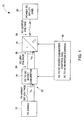
Figure 1 depicts a block diagram of a two stage PVpower inverter system 10 used to convertDC power 22 generated by aPV array 12 intoAC power 28 suitable for feeding anAC power grid 20. The first stage ofpower inverter system 10 can include a DC toDC converter 14, such as a boost converter, that providesDC power 24 to aDC link 26. TheDC link 26 couples the DC toDC converter 14 to aninverter 16 which operates as the second stage of thePV inverter system 10.Inverter 16 converts theDC power 24 on theDC link 26 toAC power 28 suitable for being supplied to anAC power grid 20. DC toDC converter 14 can be a part of or integral withinverter 16 or can be a separate stand alone structure frominverter 16. In addition, more than oneconverter 14 can be coupled to thesame inverter 16 through one or more DC links. -
PV inverter system 10 includes acontrol system 18 that is configured to control both the DC toDC boost converter 14 and the DC toAC inverter 16. For instance,control system 18 can be configured to regulate the output of the DC toDC converter 14 pursuant to a control method that adjusts the duty cycle (switching speed) of the switching devices (IGBTs or other power electronic devices) used in the DC toDC converter 14.Control system 18 can also be configured to regulate the output ofinverter 16 by varying the modulation commands provided to inverter 16. The modulation commands control the pulse width modulation of theinverter 16 and can be used to vary the real and reactive output power of theinverter 16.Control system 18 can be independent from DC toDC boost converter 14 and DC toAC inverter 16 or may be integrated into one or both of therespective system stages - When
PV inverter system 10 is operating in steady state conditions,control system 18 can regulate theDC link voltage 24 of the DC link 26 (and, correspondingly, the PV array source voltage of the PV array 12) by adjusting the AC output ofinverter 16. For instance,control system 18 can regulate theDC link voltage 24 of theDC link 26 by controlling the AC current output ofinverter 16. In steady state conditions, theinverter 16 is typically controlled to provide real power flow (i.e., the real part of the vector product of the inverter output AC voltage and the inverter output AC current) to theAC grid 20 that is equal to the power supplied to theDC link 26 by DC toDC converter 14. Varying the output AC current of theinverter 16 will result in a change to the output AC voltage of theinverter 16, based on the impedance of one or more output transformers and theutility grid 20. Adjusting the output AC voltage of theinverter 16 will correspondingly induce a change in theDC link voltage 24 of theDC link 26. - In situations in which it is necessary to accommodate a PV array 12 (or other DC power source) having a high open-circuit voltage, it is desirable to maintain the
DC link voltage 24 less than the open-circuit voltage of thePV array 12. By maintaining theDC link voltage 24 less than the open-circuit voltage of thePV array 12, the PV array source voltage provided by thePV array 12 to thePV inverter system 10 can also be maintained less than the open-circuit voltage of thePV array 12, such as at the maximum power voltage of thePV array 12. In steady-state conditions, thecontrol system 18 can regulate theDC link voltage 24 to be less than the open-circuit voltage of thePV array 12 by controlling the output ofinverter 16. Starting up a PV inverter system when the open circuit voltage of the connected PV array is very close to the blocking voltage rating of the PV inverter semiconductor power devices, e.g. array open circuit voltage is 1000Vdc and the blocking voltage of the semiconductor devices is 1200Vdc, can however be problematic due to DC link voltage overshoot. -
Figure 2 illustrates thePV inverter system 10 depicted inFigure 1 modified with power semiconductor device 38 gate current limitingresistors 40. A limiting factor when starting upPV inverter system 10 is the DC link voltage overshoot at turn-off of the semiconductor power devices 38 that may comprise, for example, insulated gate bipolar transistors (IGBT)s. TheDC link 26 voltage overshoot is generally represented by Vdc_overshoot=L*di/dt. The DC link voltage overshoot therefore is actually not dependent on the current magnitude, but on the current growth rate and the inductance in the commutation path. This voltage overshoot is only an issue at turning off the IGBT devices 38. Turning on the IGBT devices 38 does not present voltage overshoot issues. - The present inventors alone recognized that operating a PV inverter system, such as
PV inverter system 10 depicted inFigure 1 , when the open circuit voltage of the connectedPV array 12 is very close to the inverter semiconductor power device 38 blocking voltage rating, e.g. array open circuit voltage is 1000Vdc and the semiconductor power device 38 blocking voltage rating is 1200Vdc, is possible if the semiconductor power device currents are turned-off at a very low di/dt rate vialarge gate resistors 40 such as depicted inFigure 2 . The present inventors further recognized that operating the semiconductor power devices 38 in combination withlarge gate resistance 40 advantageously provides the desired low di/dt rate, but at an undesirable level of power device 38 operating efficiency; and that the foregoing undesirable losses can be reduced through a reduction of current and switching frequency during this operating mode that lasts for only a very short period of time for aPV array 12. - According to one embodiment, the large value gate resistor(s) 40 are switched back to a smaller nominal resistance value when the PV array voltage reaches its maximum power point (MPP) voltage, which is about 20% lower than the open circuit voltage of the
PV array 12. According to another embodiment, the gate resistor(s) 40 comprise variable resistance devices that linearly or non-linearly reduce the value of semiconductor power device gate resistance as the PV array voltage continues to drop in value approaching MPP voltage.Figure 5 , for example, illustrates a voltage clampinggate control architecture 100 that operates to reduce the switchingdevice gate resistances 40 in a stepwise fashion during start-up conditions as the gate voltage reduces from an initialopen circuit voltage 102 to theMPP voltage 104 according to one embodiment. - Although
Figure 2 illustrates a three-phase AC output forinverter 16, those of ordinary skill in the art, using the disclosures provided herein, should readily understand thatinverter 16 can similarly provide a single-phase AC output or other multi-phase AC output as desired without deviating from the scope of the present invention.Inverter 16 uses one or more inverter bridge circuits that include power devices 38, such as IGBTs and diodes that are used to convert the DC power onDC link 26 into a suitable AC waveform. For instance, in certain embodiments,inverter 16 uses pulse-width-modulation (PWM) to synthesize an output AC voltage at the AC grid frequency. The output ofinverter 16 can be controlled by providing gate timing commands to the IGBTs 38 of the inverter bridge circuits ofinverter 16 according to well known PWM control techniques. The output AC current flowing frominverter 16 has components at the PWM chopping frequency and the grid frequency. -
PV inverter system 10 may also include a PV array voltage sensor 42. PV array voltage sensor 42 monitors the voltage of thePV array 12 and provides feedback signals to controlsystem 18. Thecontrol system 18 can make adjustments to the semiconductor power device 38gate resistance 40 or other operating parameters ofPV inverter system 10, e.g. semiconductor power device 38 switching frequency, based on the PV array voltage detected by PV array voltage sensor 42. -
Figure 3 is a simplified block diagram illustrating aPV inverter system 50 according to another embodiment.PV inverter system 50 is similar toPV inverter system 10, exceptPV inverter system 50 does not employ a DC-DC converter such asboost converter 14 described herein with reference toFigures 1 and2 .PV inverter system 50 can be seen to include a DC to ACinverter control unit 19. According to one embodiment,inverter control unit 19 is configured to control the switching frequency of the inverter semiconductor power devices 38 and to also control the gate resistance value for each semiconductor power device 38. According to one aspect, the switching frequency is reduced below its normal operating value and the gate resistance is increased above its normal operating value when thePV array 12 open circuit voltage is very close to the semiconductor power device blocking voltage rating, e.g. array open circuit voltage is 1000Vdc and the blocking voltage of the semiconductor power devices are 1200Vdc. According to one embodiment, when the voltage generated by thePV array 12 reaches the MPP voltage, which is about 20% lower than the open circuit voltage of thePV array 12, the gate turn offresistor 40 employed during semiconductor power device 38 turn-off is switched back to a smaller value viacontrol unit 19. According to another embodiment, one ormore gate resistors 40 comprise a variable resistance device that reduces in value in response to signals received fromcontrol unit 19 as the PV array voltage output reduces in value. -
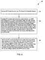
Figure 4 is a flow diagram illustrating astarting procedure 60 for thepower converter systems procedure 60 advantageously avoids any requirements for additional hardware necessary to pull down the voltage of thePV array 12 during start-up conditions. Startingprocedure 60 further advantageously negates the necessity for using semiconductor power devices with higher rated blocking voltages, e.g. 1700V IGBTs, that reduce the efficiency and increase the system cost. - With continued reference to
Figure 4 , startingprocedure 60 commences by connecting the DC voltage source,e.g. PV array 12, to thePV inverter system step 62. The DC link voltage is preferably less than the open-circuit voltage Voc ofPV array 12. According to one embodiment, thecontroller inverter 16. PV array voltage sensor(s) 42 can be used to determine ifPV array 12 is operating at an open-circuit voltage or other voltage. - Subsequent to coupling the
PV array 12 toPV inverter system controller resistance 40 of each semiconductor power device, e.g. IGBTs, during starting up period, to a value that is larger than its nominal operating value if the monitored PV array voltage is very close to the semiconductor power device blocking voltage rating, as represented instep 64. According to one embodiment, the semiconductor power device switching frequency during the respective starting up period is also reduced to a value that is lower than its nominal operating value if the monitored PV array voltage is very close to the semiconductor power device blocking voltage rating. - Upon reaching the PV array MPP tracking voltage which is about 20% lower than the open circuit voltage of the PV array,
controller step 66. According to one embodiment,controller - Those skilled in the art will readily appreciate that semiconductor power switching device gate resistance(s) and switching frequencies will depend upon the particular application, system architecture, and semiconductor power switching device(s) employed in the power inverter system. The switching characteristics and gate resistance can be accomplished with or without the use of algorithmic software, depending upon the particular application. Algorithmic software, if employed, would reside within the
controller controller AC inverter 16 that provides zero voltage at the inverter output. (e.g. a positive zero vector in a three-phase two-level DC/AC inverter occurs when all upper IGBTs are turned on and lower IGBTs are turned off. A negative zero vector will happen when all upper IGBTs are turned off and lower IGBTs are turned on). According to another embodiment, thecontroller AC inverter 16. - While only certain features of the invention have been illustrated and described herein, many modifications and changes will occur to those skilled in the art. It is, therefore, to be understood that the appended claims are intended to cover all such modifications and changes as fall within the true spirit of the invention.
- Various aspects and embodiments of the present invention are defined by the following numbered clauses:
- 1. A power inverter system, comprising:
- a DC to AC inverter comprising a plurality of power semiconductor switching devices;
- a DC link selectively coupling DC power to the inverter; and
- a controller configured to increase a gate turn off resistance for each of the power semiconductor switching devices during starting up periods of the inverter system such that the DC link voltage does not exceed the power semiconductor switching device blocking voltage ratings during the corresponding switching turn-off periods, wherein the starting up period is the time required to bring a corresponding DC power source voltage from an open circuit voltage to a predetermined voltage which constitutes a safe operating condition for the plurality of power semiconductor switching devices.
- 2. The power inverter system according to
clause 1, wherein the predetermined voltage comprises the DC power source maximum power point voltage. - 3. The power inverter system according to any preceding clause, further comprising a photovoltaic array configured to generate the DC power.
- 4. The power inverter system according to any preceding clause, wherein the controller is further configured to increase the gate turn off resistance only when the DC link voltage is within a predefmed minimum and maximum voltage value based on the blocking voltage rating of the power semiconductor switching devices.
- 5. The power inverter system according to any preceding clause, wherein the power semiconductor switching devices comprise insulated gate bipolar transistors.
- 6. The power inverter system according to any preceding clause, wherein the controller is further configured to decrease the switching frequency of the DC to AC inverter during starting up periods of the power inverter system.
- 7. The power inverter system according to any preceding clause, wherein the controller is further configured to increase the switching frequency of the DC to AC inverter when the DC link voltage is less than the predetermined voltage.
- 8. The power inverter system according to any preceding clause, wherein the predetermined voltage comprises the DC power source maximum power point voltage.
- 9. The power inverter system according to any preceding clause, wherein the controller is further configured to increase the gate turn off resistance of the power semiconductor switching devices when the DC link voltage is greater than the maximum power point voltage of the DC power source.
- 10. The power inverter system according to any preceding clause, wherein the controller is further configured to control the gate turn-off resistance for each power semiconductor switching device in a stepwise or non-stepwise fashion based upon the DC power source voltage level.
- 11. The power inverter system according to any preceding clause, wherein the controller is further configured to change the gate turn-off resistance for each power semiconductor switching device at zero vector instance of a corresponding space vector modulator, wherein zero vector is defined as the switching configuration of the power semiconductor devices in a DC to AC inverter that provides zero voltage at the inverter output.
- 12. The power inverter system according to any preceding clause, wherein the controller is further configured to increase the gate turn off resistance during a zero/low voltage ride through (ZVRT/LVRT) event of the DC to AC inverter.
- 13. A method of operating a power inverter system, the method comprising:
- providing an inverter controller and an inverter comprising a plurality of power semiconductor switching devices;
- connecting a DC voltage source to the inverter; and
- subsequent to connecting the DC voltage source to the inverter, increasing a gate turn off resistance for each of the semiconductor power switching devices during a corresponding inverter starting up period such that the source voltage does not exceed any power semiconductor switching device blocking voltage rating during the corresponding power semiconductor switching turn-off periods, wherein the starting up period is the time required to bring the DC source voltage from an open circuit voltage to a predetermined voltage which constitutes a safe operating condition for the plurality of power semiconductor switching devices.
- 14. The power inverter system according to any preceding clause, wherein the predetermined voltage comprises the DC power source maximum power point voltage.
- 15. The method according to any preceding clause, wherein the DC voltage source comprises a photovoltaic array.
- 16. The method according to any preceding clause, wherein the plurality of power semiconductor switching devices comprises insulated gate bipolar transistors.
- 17. The method according to any preceding clause, further comprising subsequent to connecting the DC voltage source to the inverter, increasing a gate turn off resistance for each of the semiconductor power switching devices only when the DC source voltage is higher than an inverter maximum dc link voltage rating such that the DC link voltage does not exceed the respective power semiconductor switching device blocking voltage rating during the corresponding switching turn-off periods.
- 18. The method according to any preceding clause, further comprising subsequent to connecting the DC voltage source to the inverter, decreasing the switching frequency for each of the semiconductor power switching devices during its corresponding starting up period such that the source voltage does not exceed the respective power semiconductor switching device blocking voltage rating during the corresponding switching turn-off periods.
- 19. A power inverter system comprising a plurality of power semiconductor switching devices, each switching device comprising a corresponding gate turn off resistance configured to increase during starting up periods of the inverter system such that the open circuit voltage of a corresponding power source providing power to the power inverter system does not exceed the switching device blocking voltage ratings during the corresponding switching turn-off periods, wherein the starting up period is the time required to bring the corresponding power source voltage from its open circuit voltage level to a predetermined voltage which constitutes a safe operating condition for the plurality of power semiconductor switching devices.
- 20. The power inverter system according to any preceding clause, wherein the predetermined voltage comprises the DC power source maximum power point voltage.
- 21. The power inverter system according to any preceding clause, wherein the power source comprises a photovoltaic array.
- 22. The power inverter system according to any preceding clause, wherein each gate turn off resistance is further configured to increase only when a corresponding inverter DC link voltage is within a predefined minimum and maximum voltage value based on the blocking voltage rating of the power semiconductor switching devices.
- 23. The power inverter system according to any preceding clause, wherein the plurality of power semiconductor switching devices comprises insulated gate bipolar transistors.
- 24. The power inverter system according to any preceding clause, wherein each power semiconductor switching device is configured to operate at a decreased switching frequency during its switching turn-off periods when the power source voltage is greater than the maximum power point voltage.
- 25. The power inverter system according to any preceding clause, wherein each power semiconductor switching device is further configured to operate at an increasing switching frequency during its switching turn-off periods as the power source voltage drops to or less than the maximum power point voltage
- 26. The power inverter system according to any preceding clause, wherein each power semiconductor switching device gate turn off resistance is further configured to decrease from its increased value as the power source voltage drops to or less than the maximum power point voltage.
- 27. The power inverter system according to any preceding clause, wherein each power semiconductor switching device gate turn off resistance is further configured to change in a stepwise or non-stepwise fashion based upon the power source voltage level.
Claims (10)
- A power inverter system (10), comprising:a DC to AC inverter (16) comprising a plurality of power semiconductor switching devices (38);a DC link (26) selectively coupling DC power to the inverter (16); anda controller (18) configured to increase a gate turn off resistance (40) for each of the power semiconductor switching devices (38) during starting up periods of the inverter system (10) such that the DC link (26) voltage does not exceed the power semiconductor switching device (38) blocking voltage ratings during the corresponding switching turn-off periods, wherein the starting up period is the time required to bring a corresponding DC power source (12) voltage from an open circuit voltage to a predetermined voltage which constitutes a safe operating condition for the plurality of power semiconductor switching devices (38).
- The power inverter system (10) according to claim 1, wherein the predetermined voltage comprises the DC power source maximum power point voltage.
- The power inverter system (10) according to any preceding claim, further comprising a photovoltaic array (12) configured to generate the DC power.
- The power inverter system (10) according to any preceding claim, wherein the controller (18) is further configured to increase the gate turn off resistance (40) only when the DC link (26) voltage is within a predefined minimum and maximum voltage value based on the blocking voltage rating of the power semiconductor switching devices (38).
- The power inverter system (10) according to any preceding claim, wherein the power semiconductor switching devices (38) comprise insulated gate bipolar transistors.
- The power inverter system (10) according to any preceding claim, wherein the controller (18) is further configured to decrease the switching frequency of the DC to AC inverter (16) during starting up periods of the power inverter system (10).
- The power inverter system (10) according to any preceding claim, wherein the controller (18) is further configured to control the gate turn-off resistance (40) for each power semiconductor switching device (38) in a stepwise or non-stepwise fashion based upon the DC power source (12) voltage level.
- The power inverter system (10) according to any preceding claim, wherein the controller (18) is further configured to change the gate turn-off resistance (40) for each power semiconductor switching device (38) at zero vector instance of a corresponding space vector modulator, wherein zero vector is defined as the switching configuration of the power semiconductor devices (38) in a DC to AC inverter (16) that provides zero voltage at the inverter (16) output.
- The power inverter system (10) according to any preceding claim, wherein the controller (18) is further configured to increase the gate turn off resistance (40) during a zero/low voltage ride through (ZVRT/LVRT) event of the DC to AC inverter (16).
- A power inverter system (10) comprising a plurality of power semiconductor switching devices (38), each switching device (38) comprising a corresponding gate turn off resistance (40) configured to increase during starting up periods of the inverter system (10) such that the open circuit voltage of a corresponding power source (12) providing power to the power inverter system (10) does not exceed the switching device (38) blocking voltage ratings during the corresponding switching turn-off periods, wherein the starting up period is the time required to bring the corresponding power source (12) voltage from its open circuit voltage level to a predetermined voltage which constitutes a safe operating condition for the plurality of power semiconductor switching devices (38).
Applications Claiming Priority (1)
| Application Number | Priority Date | Filing Date | Title |
|---|---|---|---|
| US12/870,795 US8599586B2 (en) | 2010-08-28 | 2010-08-28 | Power inverter system and method of starting same at high DC voltage |
Publications (3)
| Publication Number | Publication Date |
|---|---|
| EP2424101A2 true EP2424101A2 (en) | 2012-02-29 |
| EP2424101A3 EP2424101A3 (en) | 2017-04-12 |
| EP2424101B1 EP2424101B1 (en) | 2020-07-01 |
Family
ID=45348949
Family Applications (1)
| Application Number | Title | Priority Date | Filing Date |
|---|---|---|---|
| EP11176932.9A Active EP2424101B1 (en) | 2010-08-28 | 2011-08-09 | Power inverter system and method of starting same at high DC voltage |
Country Status (5)
| Country | Link |
|---|---|
| US (1) | US8599586B2 (en) |
| EP (1) | EP2424101B1 (en) |
| CN (1) | CN102570492B (en) |
| AU (1) | AU2011213744B2 (en) |
| ES (1) | ES2819191T3 (en) |
Cited By (2)
| Publication number | Priority date | Publication date | Assignee | Title |
|---|---|---|---|---|
| WO2014008647A1 (en) | 2012-07-12 | 2014-01-16 | General Electric Company | Dynamic braking system for an electric power system and method of operating the same |
| EP3664268A1 (en) * | 2018-12-07 | 2020-06-10 | GE Energy Power Conversion Technology Ltd. | Methods of starting an inverter system, and inverter systems |
Families Citing this family (15)
| Publication number | Priority date | Publication date | Assignee | Title |
|---|---|---|---|---|
| US9343906B2 (en) * | 2011-06-03 | 2016-05-17 | Schneider Electric Solar Inverters Usa, Inc. | High dynamic DC-voltage controller for photovoltaic inverter |
| US8537581B2 (en) * | 2011-08-25 | 2013-09-17 | General Electric Company | Power converter system and methods of operating a power converter system |
| TWI481146B (en) * | 2011-12-02 | 2015-04-11 | Darfon Electronics Corp | Off-grid solar inverter system without a battery and control method thereof |
| US9577541B2 (en) | 2012-03-20 | 2017-02-21 | Indiana University Research And Technology Corporation | Single switch infinite-level power inverters |
| US20130258718A1 (en) * | 2012-03-30 | 2013-10-03 | Advanced Energy Industries, Inc. | System, method, and apparatus for powering equipment during a low voltage event |
| US8937824B2 (en) * | 2013-01-28 | 2015-01-20 | Eaton Corporation | Photovoltaic system and method of controlling same |
| US9160173B2 (en) * | 2013-07-11 | 2015-10-13 | Renewable Power Conversion, Inc. | Photovoltaic inverter with swinging line filter inductors |
| TWI511404B (en) * | 2014-05-16 | 2015-12-01 | Nat Univ Tsing Hua | Apparatus of Low Voltage Ride-Through with Flux Chain Compensation and Current Peak Management |
| US9960686B2 (en) * | 2014-11-17 | 2018-05-01 | Infineon Technologies Austria Ag | System and method for detecting a loss of AC power in a switched-mode power supply |
| EP3051686B1 (en) * | 2015-01-27 | 2017-11-01 | ABB Schweiz AG | Method for testing electric system and electric system |
| US10148206B2 (en) * | 2016-06-27 | 2018-12-04 | General Electric Company | Controlling operation of a power converter based on grid conditions |
| JP6904091B2 (en) * | 2017-06-21 | 2021-07-14 | 富士電機株式会社 | Gate drive circuit and inverter device |
| DE102018124094A1 (en) | 2018-09-28 | 2020-04-02 | Valeo Siemens Eautomotive Germany Gmbh | Power converter, vehicle and method for operating a power converter |
| CN113452262B (en) * | 2021-07-05 | 2022-07-15 | 珠海格力电器股份有限公司 | Frequency converter, boost control method thereof and motor |
| CN114498746A (en) * | 2022-01-28 | 2022-05-13 | 浙江腾圣储能技术有限公司 | Inverter circuit, inverter control method and photovoltaic system |
Family Cites Families (16)
| Publication number | Priority date | Publication date | Assignee | Title |
|---|---|---|---|---|
| US4333136A (en) * | 1979-11-26 | 1982-06-01 | Baker Richard H | Solar powered automatic turn-on control (SPA-TOC) unit and method |
| JP3744679B2 (en) * | 1998-03-30 | 2006-02-15 | 三洋電機株式会社 | Solar power plant |
| US6291764B1 (en) | 1999-03-24 | 2001-09-18 | Sanyo Electronics Co., Ltd. | Photovoltaic power generation device |
| US6208185B1 (en) * | 1999-03-25 | 2001-03-27 | Wisconsin Alumni Research Corporation | High performance active gate drive for IGBTs |
| JP3883925B2 (en) * | 2002-07-30 | 2007-02-21 | 三菱電機株式会社 | Power semiconductor element drive circuit |
| JP4585774B2 (en) * | 2003-03-07 | 2010-11-24 | キヤノン株式会社 | Power conversion device and power supply device |
| US6914418B2 (en) * | 2003-04-21 | 2005-07-05 | Phoenixtec Power Co., Ltd. | Multi-mode renewable power converter system |
| KR101321361B1 (en) * | 2005-09-05 | 2013-10-22 | 페어차일드코리아반도체 주식회사 | Inverter module for motor drive and motor driving apparatus having the same and inverter integrated circuit package |
| DE202006001063U1 (en) | 2006-01-23 | 2006-04-27 | Institut für Solare Energieversorgungstechnik (ISET) Verein an der Universität Kassel e.V. | Inverter for feeding electrical energy from a photovoltaic unit to a three phase mains has a DC converter with maximum power point tracking control and bridge circuit |
| US7710752B2 (en) | 2006-05-23 | 2010-05-04 | Xantrex Technology Inc. | Transformerless utility-grid-interactive inverter |
| ES2327264T3 (en) | 2006-10-21 | 2009-10-27 | Sma Solar Technology Ag | ELECTRICAL CIRCUIT DEVICE AND PROCEDURE, IN PARTICULAR FOR PHOTOVOLTAIC GENERATORS. |
| JP4573843B2 (en) * | 2007-01-18 | 2010-11-04 | 株式会社豊田中央研究所 | Power semiconductor element drive circuit |
| CN101582592B (en) * | 2008-05-15 | 2013-07-10 | 宣昆 | Transformer-less photovoltaic merging and inverting device and control method thereof |
| EP2187510B1 (en) | 2008-11-15 | 2016-08-03 | SMA Solar Technology AG | Inverter start up switch |
| CN101651436B (en) * | 2009-09-16 | 2013-04-03 | 阳光电源股份有限公司 | High-precision maximum power point tracing method |
| US7855906B2 (en) * | 2009-10-26 | 2010-12-21 | General Electric Company | DC bus voltage control for two stage solar converter |
-
2010
- 2010-08-28 US US12/870,795 patent/US8599586B2/en active Active
-
2011
- 2011-08-09 ES ES11176932T patent/ES2819191T3/en active Active
- 2011-08-09 EP EP11176932.9A patent/EP2424101B1/en active Active
- 2011-08-18 AU AU2011213744A patent/AU2011213744B2/en active Active
- 2011-08-26 CN CN201110257782.3A patent/CN102570492B/en active Active
Non-Patent Citations (1)
| Title |
|---|
| None |
Cited By (5)
| Publication number | Priority date | Publication date | Assignee | Title |
|---|---|---|---|---|
| WO2014008647A1 (en) | 2012-07-12 | 2014-01-16 | General Electric Company | Dynamic braking system for an electric power system and method of operating the same |
| EP2873151B1 (en) * | 2012-07-12 | 2021-08-25 | General Electric Company | Electric power system and method of operating the same |
| EP3664268A1 (en) * | 2018-12-07 | 2020-06-10 | GE Energy Power Conversion Technology Ltd. | Methods of starting an inverter system, and inverter systems |
| WO2020115284A1 (en) * | 2018-12-07 | 2020-06-11 | Ge Energy Power Conversion Technology Ltd | Methods of starting an inverter system, and inverter systems |
| US11038438B2 (en) | 2018-12-07 | 2021-06-15 | Ge Energy Power Conversion Technology Limited | Methods of starting an inverter system, and inverter systems |
Also Published As
| Publication number | Publication date |
|---|---|
| CN102570492A (en) | 2012-07-11 |
| EP2424101B1 (en) | 2020-07-01 |
| US8599586B2 (en) | 2013-12-03 |
| US20120051101A1 (en) | 2012-03-01 |
| EP2424101A3 (en) | 2017-04-12 |
| ES2819191T3 (en) | 2021-04-15 |
| AU2011213744B2 (en) | 2014-07-24 |
| CN102570492B (en) | 2015-07-22 |
| AU2011213744A1 (en) | 2012-03-15 |
Similar Documents
| Publication | Publication Date | Title |
|---|---|---|
| EP2424101B1 (en) | Power inverter system and method of starting same at high DC voltage | |
| EP2416480B1 (en) | Photovoltaic inverter system and method of starting same at high open-circuit voltage | |
| US11201565B2 (en) | Conversion circuit, control method, and power supply device | |
| EP2395644B1 (en) | Method and system to allow for high dc source voltage with lower dc voltage in a two stage power converter | |
| EP2256579B1 (en) | Solar inverter and control method | |
| JP6206502B2 (en) | Power conversion device and power conversion method | |
| CN107567680B (en) | Variable speed drive with active converter | |
| US20130279228A1 (en) | System and method for improving low-load efficiency of high power converters | |
| US9859808B2 (en) | Power converter topology for use in an energy storage system | |
| Shojaei et al. | An improved modulation scheme for harmonic distortion reduction in modular multilevel converter | |
| KR20190072600A (en) | Hybrid rectifier | |
| US6366064B1 (en) | Dual mode controller for switching circuirty | |
| US9325273B2 (en) | Method and system for driving electric machines | |
| Oliveira et al. | A DCM three-phase high frequency semi-controlled rectifier feasible for low power WECS based on a permanent magnet generator | |
| EP3100346A1 (en) | Unidirectional matrix converter with regeneration system | |
| EP3926820A1 (en) | Component voltage limiting circuit and device applying same | |
| CN116599348A (en) | Balance bridge circuit, multi-level inversion system and balance bridge control method | |
| CN114928093A (en) | Topological structure of direct current power flow controller and control method | |
| CN114447979A (en) | Power conversion device and control method thereof | |
| Le Claire et al. | Single-phase boost-type rectifier with fault-tolerant capability | |
| CA3075059A1 (en) | Circuit for component voltage limitation, and apparatus for applying the same | |
| JP2005311956A (en) | Semiconductor switching device |
Legal Events
| Date | Code | Title | Description |
|---|---|---|---|
| AK | Designated contracting states |
Kind code of ref document: A2 Designated state(s): AL AT BE BG CH CY CZ DE DK EE ES FI FR GB GR HR HU IE IS IT LI LT LU LV MC MK MT NL NO PL PT RO RS SE SI SK SM TR |
|
| AX | Request for extension of the european patent |
Extension state: BA ME |
|
| PUAI | Public reference made under article 153(3) epc to a published international application that has entered the european phase |
Free format text: ORIGINAL CODE: 0009012 |
|
| PUAL | Search report despatched |
Free format text: ORIGINAL CODE: 0009013 |
|
| AK | Designated contracting states |
Kind code of ref document: A3 Designated state(s): AL AT BE BG CH CY CZ DE DK EE ES FI FR GB GR HR HU IE IS IT LI LT LU LV MC MK MT NL NO PL PT RO RS SE SI SK SM TR |
|
| AX | Request for extension of the european patent |
Extension state: BA ME |
|
| RIC1 | Information provided on ipc code assigned before grant |
Ipc: H02M 7/515 20070101AFI20170303BHEP |
|
| STAA | Information on the status of an ep patent application or granted ep patent |
Free format text: STATUS: REQUEST FOR EXAMINATION WAS MADE |
|
| 17P | Request for examination filed |
Effective date: 20171012 |
|
| RBV | Designated contracting states (corrected) |
Designated state(s): AL AT BE BG CH CY CZ DE DK EE ES FI FR GB GR HR HU IE IS IT LI LT LU LV MC MK MT NL NO PL PT RO RS SE SI SK SM TR |
|
| STAA | Information on the status of an ep patent application or granted ep patent |
Free format text: STATUS: EXAMINATION IS IN PROGRESS |
|
| 17Q | First examination report despatched |
Effective date: 20190219 |
|
| GRAP | Despatch of communication of intention to grant a patent |
Free format text: ORIGINAL CODE: EPIDOSNIGR1 |
|
| STAA | Information on the status of an ep patent application or granted ep patent |
Free format text: STATUS: GRANT OF PATENT IS INTENDED |
|
| INTG | Intention to grant announced |
Effective date: 20200124 |
|
| GRAS | Grant fee paid |
Free format text: ORIGINAL CODE: EPIDOSNIGR3 |
|
| GRAA | (expected) grant |
Free format text: ORIGINAL CODE: 0009210 |
|
| STAA | Information on the status of an ep patent application or granted ep patent |
Free format text: STATUS: THE PATENT HAS BEEN GRANTED |
|
| AK | Designated contracting states |
Kind code of ref document: B1 Designated state(s): AL AT BE BG CH CY CZ DE DK EE ES FI FR GB GR HR HU IE IS IT LI LT LU LV MC MK MT NL NO PL PT RO RS SE SI SK SM TR |
|
| REG | Reference to a national code |
Ref country code: GB Ref legal event code: FG4D |
|
| REG | Reference to a national code |
Ref country code: CH Ref legal event code: EP Ref country code: AT Ref legal event code: REF Ref document number: 1287124 Country of ref document: AT Kind code of ref document: T Effective date: 20200715 |
|
| REG | Reference to a national code |
Ref country code: IE Ref legal event code: FG4D |
|
| REG | Reference to a national code |
Ref country code: DE Ref legal event code: R096 Ref document number: 602011067547 Country of ref document: DE |
|
| REG | Reference to a national code |
Ref country code: LT Ref legal event code: MG4D |
|
| PG25 | Lapsed in a contracting state [announced via postgrant information from national office to epo] |
Ref country code: BG Free format text: LAPSE BECAUSE OF FAILURE TO SUBMIT A TRANSLATION OF THE DESCRIPTION OR TO PAY THE FEE WITHIN THE PRESCRIBED TIME-LIMIT Effective date: 20201001 |
|
| REG | Reference to a national code |
Ref country code: NL Ref legal event code: MP Effective date: 20200701 |
|
| REG | Reference to a national code |
Ref country code: AT Ref legal event code: MK05 Ref document number: 1287124 Country of ref document: AT Kind code of ref document: T Effective date: 20200701 |
|
| PG25 | Lapsed in a contracting state [announced via postgrant information from national office to epo] |
Ref country code: LT Free format text: LAPSE BECAUSE OF FAILURE TO SUBMIT A TRANSLATION OF THE DESCRIPTION OR TO PAY THE FEE WITHIN THE PRESCRIBED TIME-LIMIT Effective date: 20200701 Ref country code: CZ Free format text: LAPSE BECAUSE OF FAILURE TO SUBMIT A TRANSLATION OF THE DESCRIPTION OR TO PAY THE FEE WITHIN THE PRESCRIBED TIME-LIMIT Effective date: 20200701 Ref country code: PT Free format text: LAPSE BECAUSE OF FAILURE TO SUBMIT A TRANSLATION OF THE DESCRIPTION OR TO PAY THE FEE WITHIN THE PRESCRIBED TIME-LIMIT Effective date: 20201102 Ref country code: AT Free format text: LAPSE BECAUSE OF FAILURE TO SUBMIT A TRANSLATION OF THE DESCRIPTION OR TO PAY THE FEE WITHIN THE PRESCRIBED TIME-LIMIT Effective date: 20200701 Ref country code: HR Free format text: LAPSE BECAUSE OF FAILURE TO SUBMIT A TRANSLATION OF THE DESCRIPTION OR TO PAY THE FEE WITHIN THE PRESCRIBED TIME-LIMIT Effective date: 20200701 Ref country code: FI Free format text: LAPSE BECAUSE OF FAILURE TO SUBMIT A TRANSLATION OF THE DESCRIPTION OR TO PAY THE FEE WITHIN THE PRESCRIBED TIME-LIMIT Effective date: 20200701 Ref country code: NO Free format text: LAPSE BECAUSE OF FAILURE TO SUBMIT A TRANSLATION OF THE DESCRIPTION OR TO PAY THE FEE WITHIN THE PRESCRIBED TIME-LIMIT Effective date: 20201001 Ref country code: GR Free format text: LAPSE BECAUSE OF FAILURE TO SUBMIT A TRANSLATION OF THE DESCRIPTION OR TO PAY THE FEE WITHIN THE PRESCRIBED TIME-LIMIT Effective date: 20201002 Ref country code: SE Free format text: LAPSE BECAUSE OF FAILURE TO SUBMIT A TRANSLATION OF THE DESCRIPTION OR TO PAY THE FEE WITHIN THE PRESCRIBED TIME-LIMIT Effective date: 20200701 |
|
| PG25 | Lapsed in a contracting state [announced via postgrant information from national office to epo] |
Ref country code: RS Free format text: LAPSE BECAUSE OF FAILURE TO SUBMIT A TRANSLATION OF THE DESCRIPTION OR TO PAY THE FEE WITHIN THE PRESCRIBED TIME-LIMIT Effective date: 20200701 Ref country code: LV Free format text: LAPSE BECAUSE OF FAILURE TO SUBMIT A TRANSLATION OF THE DESCRIPTION OR TO PAY THE FEE WITHIN THE PRESCRIBED TIME-LIMIT Effective date: 20200701 Ref country code: PL Free format text: LAPSE BECAUSE OF FAILURE TO SUBMIT A TRANSLATION OF THE DESCRIPTION OR TO PAY THE FEE WITHIN THE PRESCRIBED TIME-LIMIT Effective date: 20200701 Ref country code: IS Free format text: LAPSE BECAUSE OF FAILURE TO SUBMIT A TRANSLATION OF THE DESCRIPTION OR TO PAY THE FEE WITHIN THE PRESCRIBED TIME-LIMIT Effective date: 20201101 |
|
| PG25 | Lapsed in a contracting state [announced via postgrant information from national office to epo] |
Ref country code: NL Free format text: LAPSE BECAUSE OF FAILURE TO SUBMIT A TRANSLATION OF THE DESCRIPTION OR TO PAY THE FEE WITHIN THE PRESCRIBED TIME-LIMIT Effective date: 20200701 Ref country code: MC Free format text: LAPSE BECAUSE OF FAILURE TO SUBMIT A TRANSLATION OF THE DESCRIPTION OR TO PAY THE FEE WITHIN THE PRESCRIBED TIME-LIMIT Effective date: 20200701 |
|
| REG | Reference to a national code |
Ref country code: CH Ref legal event code: PL |
|
| REG | Reference to a national code |
Ref country code: DE Ref legal event code: R097 Ref document number: 602011067547 Country of ref document: DE |
|
| REG | Reference to a national code |
Ref country code: ES Ref legal event code: FG2A Ref document number: 2819191 Country of ref document: ES Kind code of ref document: T3 Effective date: 20210415 |
|
| PG25 | Lapsed in a contracting state [announced via postgrant information from national office to epo] |
Ref country code: DK Free format text: LAPSE BECAUSE OF FAILURE TO SUBMIT A TRANSLATION OF THE DESCRIPTION OR TO PAY THE FEE WITHIN THE PRESCRIBED TIME-LIMIT Effective date: 20200701 Ref country code: CH Free format text: LAPSE BECAUSE OF NON-PAYMENT OF DUE FEES Effective date: 20200831 Ref country code: EE Free format text: LAPSE BECAUSE OF FAILURE TO SUBMIT A TRANSLATION OF THE DESCRIPTION OR TO PAY THE FEE WITHIN THE PRESCRIBED TIME-LIMIT Effective date: 20200701 Ref country code: LI Free format text: LAPSE BECAUSE OF NON-PAYMENT OF DUE FEES Effective date: 20200831 Ref country code: LU Free format text: LAPSE BECAUSE OF NON-PAYMENT OF DUE FEES Effective date: 20200809 Ref country code: SM Free format text: LAPSE BECAUSE OF FAILURE TO SUBMIT A TRANSLATION OF THE DESCRIPTION OR TO PAY THE FEE WITHIN THE PRESCRIBED TIME-LIMIT Effective date: 20200701 Ref country code: RO Free format text: LAPSE BECAUSE OF FAILURE TO SUBMIT A TRANSLATION OF THE DESCRIPTION OR TO PAY THE FEE WITHIN THE PRESCRIBED TIME-LIMIT Effective date: 20200701 |
|
| PLBE | No opposition filed within time limit |
Free format text: ORIGINAL CODE: 0009261 |
|
| STAA | Information on the status of an ep patent application or granted ep patent |
Free format text: STATUS: NO OPPOSITION FILED WITHIN TIME LIMIT |
|
| REG | Reference to a national code |
Ref country code: BE Ref legal event code: MM Effective date: 20200831 |
|
| PG25 | Lapsed in a contracting state [announced via postgrant information from national office to epo] |
Ref country code: AL Free format text: LAPSE BECAUSE OF FAILURE TO SUBMIT A TRANSLATION OF THE DESCRIPTION OR TO PAY THE FEE WITHIN THE PRESCRIBED TIME-LIMIT Effective date: 20200701 |
|
| 26N | No opposition filed |
Effective date: 20210406 |
|
| PG25 | Lapsed in a contracting state [announced via postgrant information from national office to epo] |
Ref country code: SK Free format text: LAPSE BECAUSE OF FAILURE TO SUBMIT A TRANSLATION OF THE DESCRIPTION OR TO PAY THE FEE WITHIN THE PRESCRIBED TIME-LIMIT Effective date: 20200701 |
|
| PG25 | Lapsed in a contracting state [announced via postgrant information from national office to epo] |
Ref country code: BE Free format text: LAPSE BECAUSE OF NON-PAYMENT OF DUE FEES Effective date: 20200831 Ref country code: IE Free format text: LAPSE BECAUSE OF NON-PAYMENT OF DUE FEES Effective date: 20200809 Ref country code: SI Free format text: LAPSE BECAUSE OF FAILURE TO SUBMIT A TRANSLATION OF THE DESCRIPTION OR TO PAY THE FEE WITHIN THE PRESCRIBED TIME-LIMIT Effective date: 20200701 |
|
| PG25 | Lapsed in a contracting state [announced via postgrant information from national office to epo] |
Ref country code: TR Free format text: LAPSE BECAUSE OF FAILURE TO SUBMIT A TRANSLATION OF THE DESCRIPTION OR TO PAY THE FEE WITHIN THE PRESCRIBED TIME-LIMIT Effective date: 20200701 Ref country code: MT Free format text: LAPSE BECAUSE OF FAILURE TO SUBMIT A TRANSLATION OF THE DESCRIPTION OR TO PAY THE FEE WITHIN THE PRESCRIBED TIME-LIMIT Effective date: 20200701 Ref country code: CY Free format text: LAPSE BECAUSE OF FAILURE TO SUBMIT A TRANSLATION OF THE DESCRIPTION OR TO PAY THE FEE WITHIN THE PRESCRIBED TIME-LIMIT Effective date: 20200701 |
|
| PG25 | Lapsed in a contracting state [announced via postgrant information from national office to epo] |
Ref country code: MK Free format text: LAPSE BECAUSE OF FAILURE TO SUBMIT A TRANSLATION OF THE DESCRIPTION OR TO PAY THE FEE WITHIN THE PRESCRIBED TIME-LIMIT Effective date: 20200701 |
|
| P01 | Opt-out of the competence of the unified patent court (upc) registered |
Effective date: 20230522 |
|
| PGFP | Annual fee paid to national office [announced via postgrant information from national office to epo] |
Ref country code: IT Payment date: 20230720 Year of fee payment: 13 Ref country code: GB Payment date: 20230720 Year of fee payment: 13 Ref country code: ES Payment date: 20230901 Year of fee payment: 13 |
|
| PGFP | Annual fee paid to national office [announced via postgrant information from national office to epo] |
Ref country code: FR Payment date: 20230720 Year of fee payment: 13 Ref country code: DE Payment date: 20230720 Year of fee payment: 13 |
|
| REG | Reference to a national code |
Ref country code: DE Ref legal event code: R081 Ref document number: 602011067547 Country of ref document: DE Owner name: GE GRID SOLUTIONS LLC, ATLANTA, US Free format text: FORMER OWNER: GENERAL ELECTRIC COMPANY, SCHENECTADY, NY, US |
|
| REG | Reference to a national code |
Ref country code: GB Ref legal event code: 732E Free format text: REGISTERED BETWEEN 20231207 AND 20231213 |