EP2424043A1 - Antenna structure - Google Patents
Antenna structure Download PDFInfo
- Publication number
- EP2424043A1 EP2424043A1 EP10189978A EP10189978A EP2424043A1 EP 2424043 A1 EP2424043 A1 EP 2424043A1 EP 10189978 A EP10189978 A EP 10189978A EP 10189978 A EP10189978 A EP 10189978A EP 2424043 A1 EP2424043 A1 EP 2424043A1
- Authority
- EP
- European Patent Office
- Prior art keywords
- antenna
- radiation unit
- metal plate
- antenna structure
- substrate
- Prior art date
- Legal status (The legal status is an assumption and is not a legal conclusion. Google has not performed a legal analysis and makes no representation as to the accuracy of the status listed.)
- Pending
Links
Images


Classifications
-
- H—ELECTRICITY
- H01—ELECTRIC ELEMENTS
- H01Q—ANTENNAS, i.e. RADIO AERIALS
- H01Q9/00—Electrically-short antennas having dimensions not more than twice the operating wavelength and consisting of conductive active radiating elements
- H01Q9/04—Resonant antennas
- H01Q9/0407—Substantially flat resonant element parallel to ground plane, e.g. patch antenna
-
- H—ELECTRICITY
- H01—ELECTRIC ELEMENTS
- H01Q—ANTENNAS, i.e. RADIO AERIALS
- H01Q1/00—Details of, or arrangements associated with, antennas
- H01Q1/12—Supports; Mounting means
- H01Q1/22—Supports; Mounting means by structural association with other equipment or articles
- H01Q1/2258—Supports; Mounting means by structural association with other equipment or articles used with computer equipment
- H01Q1/2266—Supports; Mounting means by structural association with other equipment or articles used with computer equipment disposed inside the computer
-
- H—ELECTRICITY
- H01—ELECTRIC ELEMENTS
- H01Q—ANTENNAS, i.e. RADIO AERIALS
- H01Q13/00—Waveguide horns or mouths; Slot antennas; Leaky-waveguide antennas; Equivalent structures causing radiation along the transmission path of a guided wave
- H01Q13/10—Resonant slot antennas
Definitions
- the present invention relates to an antenna structure, and more particularly to an antenna structure capable of enhancing the radiation effect of the entire antenna.
- wireless communication devices such as mobile phones, notebook computers, personal digital assistants (PDAs), GPS Satellite Navigation Systems, and E-book readers.
- PDAs personal digital assistants
- E-book readers E-book readers
- the housing of electric devices is expected to be made of metal, or be plated with a metal layer, influences the quality of wireless communication. Due to the shielding effect of metal, the delivery of electromagnetic waves is blocked, and antenna signal quality suffers.
- the present invention is directed to an antenna structure so as to enhance the antenna gain and increase the bandwidth or provide multiple modes.
- the present invention is further directed to an antenna structure so as to enable an electronic device to have pleasing housing without reducing the gain of the antenna when being applied in the electronic device.
- An antenna structure which includes: a substrate; a radiation unit, disposed on the substrate; and a metal plate, separated from the radiation unit for a distance and electrically isolated with the radiation unit.
- the metal plate is excited by the radiation unit to generate at least one resonance mode, and the metal plate includes a hole penetrating the metal plate.
- An antenna structure which includes: a radiation unit; and a metal cover, including a concave surface and a convex surface.
- the concave surface faces the radiation unit.
- the metal cover is electrically isolated with the radiation unit and is excited by the radiation unit to generate at least one resonance mode.
- the metal cover includes a hole penetrating the concave surface and the convex surface.
- FIG. 3 is a schematic view of a first embodiment of the present invention
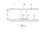
- FIG. 4 is a side view of the first embodiment of the present invention.
- the antenna structure 1 includes a substrate 12, a radiation unit 14, and a metal plate 16.
- the radiation unit 14 is disposed on the substrate 12.
- the metal plate 16 is separated from the radiation unit 14 for a distance d, and is electrically isolated with the radiation unit 14.
- a capacity effect is generated between the metal plate 16 and the radiation unit 14.
- the metal plate 16 is excited by the radiation unit 14, such that the antenna structure 1 generates at least one resonance mode.
- the metal plate 16 includes a hole 162 penetrating the metal plate 16, and the metal plate 16 cannot be fed with any electric signal or be grounded.
- the metal plate 16 having the hole 162 couples the electromagnetic wave signals, and sends the electromagnetic wave signals with a radiation area larger than the radiation unit 14. Therefore, the gain of the radiation unit 14 is increased, and the quality of communication is improved.
- the metal plate 16 when receiving the electromagnetic wave signals, provides a larger area to receive the electromagnetic wave signals, and thus the quality of the signals are improved.
- the metal plate 16 couples the electromagnetic wave signals to the radiation unit 14 and converts the electromagnetic wave signals into electric signals.
- the radiation unit 14 must be separated from the metal plate 16 for a distance d, so as to prevent the two being too far away from each other to couple the electromagnetic wave signals; or the two are too close to each other such that the radiated electromagnetic wave signals has a strength exceeding the official standard.
- the shape of the hole 162 may be a geometrical shape, such as circle and square, and may also be an irregular shape, for example, be designed to a shape of a trademark.
- the hole 162 cannot be connected to edges of the metal plate 16, that is, the hole 162 must be a hole with closed surroundings.
- the hole 162 is projected orthogonally to the substrate 12 to form a projection part 164, and at least part of the projection part 164 is overlapped with the radiation unit 14.
- the radiation unit 14 is selected from a group consisting of a microstrip antenna, a slot antenna, a monopole antenna, a dipole antenna, a patch antenna, a loop antenna, and an array antenna.
- the antenna structure 1 further includes a fixing member (not shown), which is connected to at least one of the substrate 12 and the metal plate 16, so as to maintain a distance between the metal plate 16 and the radiation unit 14.
- the fixing member may be member for supporting and fixing the substrate 12 or the metal plate 16, such as, a support, a screw stud, and a screw thread.
- the metal plate 16 may be connected to a housing of the electronic device or become a part of the housing.
- the material of the metal plate 16 may be magnesium, aluminum, stainless steel, or an alloy thereof.
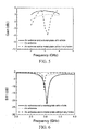
- FIG. 5 is a gain comparison view of the first embodiment, in which comparison is performed on the gain charts of only a radiation unit 14 and a radiation unit 14 in cooperation with a metal plate without a hole. It can be seen that although in the frequency bands of 2 GHz-4 GHz, 2.2 GHz-2.9 GHz, and 3.6 GHz-4 GHz, the metal plate without a hole is helpful to increase the gain, in the frequency band of 2.9 GHz-3.6 GHz, the gain is reduced significantly. However, the antenna structure 1 of the present invention can improve the gain significantly in the frequency band of 2 GHz-4 GHz. It can be seen that the antenna structure 1 of the present invention actually has good communication capability.
- FIG. 6 is a return loss comparison view of the first embodiment of the present invention, in which a comparison is performed on the gain charts of the radiation unit 14 and the radiation unit 14 in cooperation with a metal plate without a hole. It can be seen that, although the metal plate without a hole is added above the radiation unit 14, and the return loss in the frequency band of 2.8 GHz-3 GHz is reduced, the return loss in other frequency band is higher than that of the radiation unit 14. On the contrary, the antenna structure 1 of the present invention reduces the return los in the frequency band of 3.7 GHz-4 GHz, especially at a frequency of 3.05 GHz, the antenna structure 1 of the present invention reduces the return loss to -22dB. This further indicates that the antenna structure 1 of the present invention actually has good communication capability.
- the antenna structure 1 of the present invention when the antenna structure 1 of the present invention is added with the metal plate 16, a capacity effect is generated between the radiation unit 14 and the metal plate 16, and a good resistance match is obtained. Therefore, at least one resonance mode is generated, and the resonance mode can provide a larger bandwidth and gain.
- the radiation unit 14 in FIGs. 5 and 6 are the same.
- a microstrip antenna is taken as an example for measurement, but the present invention is not limited thereto.
- FIG. 7 is a side view of a second embodiment of the present invention.
- a metal plate 16 may further have at least one side plate 166 extended, for example, two opposite sides of the metal plate 16 have two side plates 166 extended to form a U shape in side view. Alternatively, only one side plate 166 extends and forms an L shape (not shown) in side view.
- the metal plate 16 may be, for example, but not limited to, a geometrical shape, such as square and circle, or other irregular shapes.
- FIG. 8 is a schematic view of a third embodiment of the present invention.
- a notebook computer 2 is taken as an example to illustrate how to apply the antenna structure of the present invention.
- the metal plate 16 may be a part of a back housing 22 of the notebook computer 2.
- the material of the back housing 22 may be plastic, carbon fiber, or magnalium, and the metal plate 16 may be connected to the back housing 22 in an embedding manner.
- a radiation unit (not shown), of the notebook computer 2 is generally disposed inside the back housing 22 above the screen, and the metal plate 16 is disposed above the radiation unit and is combined with the back housing 22, such that the gain of the radiation unit is improved, and a desired figure of the product is obtained.
- the metal plate 16 and the back housing 22 may also be formed integrally.
- FIGs. 9 and 10 are respectively a schematic view and a side view of a fourth embodiment of the present invention.
- the antenna structure 3 includes a radiation unit 32 and a metal cover 34.
- the radiation unit 32 includes a feed part and a radiation part (not shown).
- the feed part is used for feeding electric signals.
- the radiation part is connected electrically to the feed part, so as to convert the electric signals into electromagnetic wave signals and send the electromagnetic wave signals. Alternatively, after the radiation part receives the electromagnetic wave signals, the feed part converts the electromagnetic wave signals into electric signals and outputs the electric signals.
- the radiation unit 32 may further includes a grounding part (not shown), which is connected electrically to the radiation part, so as to be connected electrically to a grounding level.
- the radiation unit 32 is selected from a group consisting of a microstrip antenna, a slot antenna, a monopole antenna, a dipole antenna, a patch antenna, a loop antenna, a spiral antenna, a coaxial antenna, a chip antenna, and an array antenna.
- the metal cover 34 includes a concave surface 342 and a convex surface 344.
- the concave surface 342 faces the radiation unit 32.
- the metal cover 34 is electrically isolated with the radiation unit 32, and is excited by the radiation unit 32 in the manner of energy coupling, so as to generate at least one resonance mode.
- the metal cover 34 includes a hole 346 penetrating the concave surface 342 and the convex surface 344.
- the metal cover 34 cannot be fed with any electric signals or be grounded.
- the material of the metal cover 34 may be magnesium, aluminum, stainless steel, or an alloy thereof.
- the shape of the metal cover 34 in FIG. 9 is described as semi-spherical for convenience, which is not intended to limit the present invention.
- the metal cover 34 with the hole 346 couples the electromagnetic wave signals, and sends the electromagnetic wave signals with a radiation area larger than the radiation unit 32.
- the gain of the radiation unit 32 is thus increased.
- the metal cover 34 provides a large area to receive the electromagnetic wave signals. Therefore, the quality of communication of the radiation unit 32 is improved by the metal cover 34.
- the metal cover 34 couples the electromagnetic wave signals to the radiation unit 32 and converts the electromagnetic wave signals into electric signals.
- the radiation unit 32 must be separated from the hole 346 of the metal cover 34 for a distance, so as to prevent that the two are too far away from each other to couple the electromagnetic wave signals; or the two are too close to each other such that the radiated electromagnetic wave signals has a strength exceeding the official standard.
- the shape of the hole 346 may be a geometrical shape, such as circle and square, and may also be an irregular shape, for example, be designed to a shape of a trademark.
- the hole 346 cannot be connected to edges of the metal plate 16, that is, the hole 346 must be a hole with closed surroundings.
- the hole 346 is projected orthogonally to the radiation unit 32 to form a projection part 348, and the projection part 348 is at least partially overlapped with the radiation unit 32.
- FIG. 11 is a schematic view of a fifth embodiment of the present invention.
- an antenna structure according to the fifth embodiment of the present invention further includes a substrate 36, and a radiation unit 32 is disposed on the substrate 36.
- a metal cover 34 is connected to the substrate 36, but is electrically isolated with the substrate 36 or other electric signal lines on the substrate 36, so as to maintain the distance between the hole 346 and the radiation unit 32.
- the metal cover 34 and the substrate 36 may be connected through welding, binding, locking with bolt.
- FIG. 12 is a schematic view of a sixth embodiment of the present invention.
- a metal cover 34 according to the sixth embodiment of the present invention also includes a concave surface 342 and a convex surface 344.
- the metal cover 34 may be in a form of cylindrical paraboloid.
- the concave surface 342 faces a radiation unit 32, and a metal cover 34 also includes a hole 346 penetrating the concave surface 342 and the convex surface 344.
- the antenna structure according to the sixth embodiment of the present invention may also further include a substrate 36, as described in the fourth embodiment of the present invention.
- the communication capability of the antenna is actually improved with a metal plate having a hole or a metal cover, and the metal plate is applied in the housing of electronic devices to improve the degree of freedom in appearance design of electronic devices.
Landscapes
- Engineering & Computer Science (AREA)
- Computer Hardware Design (AREA)
- General Engineering & Computer Science (AREA)
- Waveguide Aerials (AREA)
- Support Of Aerials (AREA)
- Details Of Aerials (AREA)
Abstract
An antenna structure includes a substrate (12), a radiation unit (14), and a metal plate (16). The radiation unit is disposed on the substrate. The metal plate is separated from the radiation unit for a distance and is electrically isolated with the radiation unit. The metal plate is excited by the radiation unit to generate at least one resonance mode, and includes a hole (162) penetrating the metal plate. Thus, the gain is enhanced, the bandwidth is increased, and multiple resonance modes are provided.
Description
- The present invention relates to an antenna structure, and more particularly to an antenna structure capable of enhancing the radiation effect of the entire antenna.
- With the development of wireless communication technologies, many wireless communication devices, such as mobile phones, notebook computers, personal digital assistants (PDAs), GPS Satellite Navigation Systems, and E-book readers, have been developed. Aside from wireless communication functions, by replacing a conventional external antenna with an embedded antenna, the wireless communication devices can be built with an attractive, light, and thin industrial design while having a good quality of wireless communication.
- However, in order to ensure an attractive design with accompanying sensation of quality, the housing of electric devices is expected to be made of metal, or be plated with a metal layer, influences the quality of wireless communication. Due to the shielding effect of metal, the delivery of electromagnetic waves is blocked, and antenna signal quality suffers.
-
FIG. 1 is a schematic view of a conventional wireless communication device 1a. Presently, in order to solve the above problem ahousing 12a must have anon-metal portion 122a and ametal portion 124a. Thenon-metal portion 122a is made of a non-metal material such as plastic and carbon fiber, so that electromagnetic waves may be received by an antenna (not shown), in thehousing 12a through thenon-metal portion 122a, or electromagnetic waves radiated by the antenna may be radiated out through a hole 14a. -
FIG. 2 is a schematic view ofUS Patent Application Publication No. 20100141535 . Please refer toFIG. 2 , in which ametal sheet 24a is disposed on ahousing 22a of anelectronic device 2a to improve the field pattern and the average gain of anantenna 26a in thehousing 22a. However, themetal sheet 24a must avoid being overlapped excessively with theantenna 26a, otherwise it is not possible to improve the efficacy of antenna gain, and the shielding effect described above will result. - Accordingly, the present invention is directed to an antenna structure so as to enhance the antenna gain and increase the bandwidth or provide multiple modes. The present invention is further directed to an antenna structure so as to enable an electronic device to have pleasing housing without reducing the gain of the antenna when being applied in the electronic device.
- An antenna structure is provided, which includes: a substrate; a radiation unit, disposed on the substrate; and a metal plate, separated from the radiation unit for a distance and electrically isolated with the radiation unit. The metal plate is excited by the radiation unit to generate at least one resonance mode, and the metal plate includes a hole penetrating the metal plate.
- An antenna structure is provided, which includes: a radiation unit; and a metal cover, including a concave surface and a convex surface. The concave surface faces the radiation unit. The metal cover is electrically isolated with the radiation unit and is excited by the radiation unit to generate at least one resonance mode. The metal cover includes a hole penetrating the concave surface and the convex surface.
- Preferred embodiments and effects of the present invention are illustrated below with reference to the accompanying drawings.
- The present invention will become more fully understood from the detailed description given below for illustration only, and thus not limitative of the present invention, wherein:
-
FIG. 1 is a schematic view of a conventional communication unit; -
FIG. 2 is a schematic view ofUS Patent Application Publication No. 20100141535 ; -
FIG. 3 is a schematic view of a first embodiment of the present invention; -
FIG. 4 is side view of the first embodiment of the present invention; -
FIG. 5 is a gain comparison view of the first embodiment of the present invention; -
FIG. 6 is a return loss comparison view of the first embodiment of the present invention; -
FIG. 7 is a side view of a second embodiment of the present invention; -
FIG. 8 is a schematic view of a third embodiment of the present invention; -
FIG. 9 is a schematic view of a fourth embodiment of the present invention; -
FIG. 10 is a side view of the fourth embodiment of the present invention; -
FIG. 11 is a schematic view of a fifth embodiment of the present invention; and -
FIG. 12 is a schematic view of a sixth embodiment of the present invention. - Hereafter embodiments are exemplified to illustrate the present invention in detail with reference to the accompanying drawings. For numbers mentioned in the specification, please make reference to the reference numbers in the drawings.
-
FIG. 3 is a schematic view of a first embodiment of the present invention, andFIG. 4 is a side view of the first embodiment of the present invention. Please refer toFIGs. 3 and4 , in which the first embodiment provides anantenna structure 1. Theantenna structure 1 includes asubstrate 12, aradiation unit 14, and ametal plate 16. Theradiation unit 14 is disposed on thesubstrate 12. Themetal plate 16 is separated from theradiation unit 14 for a distance d, and is electrically isolated with theradiation unit 14. A capacity effect is generated between themetal plate 16 and theradiation unit 14. In the manner of energy coupling, themetal plate 16 is excited by theradiation unit 14, such that theantenna structure 1 generates at least one resonance mode. Themetal plate 16 includes ahole 162 penetrating themetal plate 16, and themetal plate 16 cannot be fed with any electric signal or be grounded. - When the
radiation unit 14 radiates electromagnetic wave signals, themetal plate 16 having thehole 162 couples the electromagnetic wave signals, and sends the electromagnetic wave signals with a radiation area larger than theradiation unit 14. Therefore, the gain of theradiation unit 14 is increased, and the quality of communication is improved. On the other hand, when receiving the electromagnetic wave signals, themetal plate 16 provides a larger area to receive the electromagnetic wave signals, and thus the quality of the signals are improved. Themetal plate 16 couples the electromagnetic wave signals to theradiation unit 14 and converts the electromagnetic wave signals into electric signals. Here, theradiation unit 14 must be separated from themetal plate 16 for a distance d, so as to prevent the two being too far away from each other to couple the electromagnetic wave signals; or the two are too close to each other such that the radiated electromagnetic wave signals has a strength exceeding the official standard. - The shape of the
hole 162 may be a geometrical shape, such as circle and square, and may also be an irregular shape, for example, be designed to a shape of a trademark. Thehole 162 cannot be connected to edges of themetal plate 16, that is, thehole 162 must be a hole with closed surroundings. Thehole 162 is projected orthogonally to thesubstrate 12 to form aprojection part 164, and at least part of theprojection part 164 is overlapped with theradiation unit 14. Theradiation unit 14 is selected from a group consisting of a microstrip antenna, a slot antenna, a monopole antenna, a dipole antenna, a patch antenna, a loop antenna, and an array antenna. - Furthermore, the
antenna structure 1 further includes a fixing member (not shown), which is connected to at least one of thesubstrate 12 and themetal plate 16, so as to maintain a distance between themetal plate 16 and theradiation unit 14. Here, the fixing member may be member for supporting and fixing thesubstrate 12 or themetal plate 16, such as, a support, a screw stud, and a screw thread. Moreover, when theantenna structure 1 is applied in an electronic device themetal plate 16 may be connected to a housing of the electronic device or become a part of the housing. The material of themetal plate 16 may be magnesium, aluminum, stainless steel, or an alloy thereof. -
FIG. 5 is a gain comparison view of the first embodiment, in which comparison is performed on the gain charts of only aradiation unit 14 and aradiation unit 14 in cooperation with a metal plate without a hole. It can be seen that although in the frequency bands of 2 GHz-4 GHz, 2.2 GHz-2.9 GHz, and 3.6 GHz-4 GHz, the metal plate without a hole is helpful to increase the gain, in the frequency band of 2.9 GHz-3.6 GHz, the gain is reduced significantly. However, theantenna structure 1 of the present invention can improve the gain significantly in the frequency band of 2 GHz-4 GHz. It can be seen that theantenna structure 1 of the present invention actually has good communication capability. -
FIG. 6 is a return loss comparison view of the first embodiment of the present invention, in which a comparison is performed on the gain charts of theradiation unit 14 and theradiation unit 14 in cooperation with a metal plate without a hole. It can be seen that, although the metal plate without a hole is added above theradiation unit 14, and the return loss in the frequency band of 2.8 GHz-3 GHz is reduced, the return loss in other frequency band is higher than that of theradiation unit 14. On the contrary, theantenna structure 1 of the present invention reduces the return los in the frequency band of 3.7 GHz-4 GHz, especially at a frequency of 3.05 GHz, theantenna structure 1 of the present invention reduces the return loss to -22dB. This further indicates that theantenna structure 1 of the present invention actually has good communication capability. - Compared with a
single radiation unit 14, when theantenna structure 1 of the present invention is added with themetal plate 16, a capacity effect is generated between theradiation unit 14 and themetal plate 16, and a good resistance match is obtained. Therefore, at least one resonance mode is generated, and the resonance mode can provide a larger bandwidth and gain. - Here, the
radiation unit 14 inFIGs. 5 and 6 are the same. In order to clearly indicate the efficacy of theantenna structure 1 of the present invention, compared with the difference of only theradiation unit 14 or theradiation unit 14 in cooperation with a metal plate, a microstrip antenna is taken as an example for measurement, but the present invention is not limited thereto. -
FIG. 7 is a side view of a second embodiment of the present invention. Like theantenna structure 1 according to the first embodiment of the present invention, ametal plate 16 may further have at least oneside plate 166 extended, for example, two opposite sides of themetal plate 16 have twoside plates 166 extended to form a U shape in side view. Alternatively, only oneside plate 166 extends and forms an L shape (not shown) in side view. Moreover, themetal plate 16 may be, for example, but not limited to, a geometrical shape, such as square and circle, or other irregular shapes. -
FIG. 8 is a schematic view of a third embodiment of the present invention. Anotebook computer 2 is taken as an example to illustrate how to apply the antenna structure of the present invention. Themetal plate 16 may be a part of aback housing 22 of thenotebook computer 2. The material of theback housing 22 may be plastic, carbon fiber, or magnalium, and themetal plate 16 may be connected to theback housing 22 in an embedding manner. A radiation unit (not shown), of thenotebook computer 2 is generally disposed inside theback housing 22 above the screen, and themetal plate 16 is disposed above the radiation unit and is combined with theback housing 22, such that the gain of the radiation unit is improved, and a desired figure of the product is obtained. Here, themetal plate 16 and theback housing 22 may also be formed integrally. -
FIGs. 9 and 10 are respectively a schematic view and a side view of a fourth embodiment of the present invention. Please refer toFIGs. 9 and 10 , in which the fourth embodiment provides anantenna structure 3. Theantenna structure 3 includes aradiation unit 32 and ametal cover 34. Theradiation unit 32 includes a feed part and a radiation part (not shown). The feed part is used for feeding electric signals. The radiation part is connected electrically to the feed part, so as to convert the electric signals into electromagnetic wave signals and send the electromagnetic wave signals. Alternatively, after the radiation part receives the electromagnetic wave signals, the feed part converts the electromagnetic wave signals into electric signals and outputs the electric signals. Here, theradiation unit 32 may further includes a grounding part (not shown), which is connected electrically to the radiation part, so as to be connected electrically to a grounding level. Theradiation unit 32 is selected from a group consisting of a microstrip antenna, a slot antenna, a monopole antenna, a dipole antenna, a patch antenna, a loop antenna, a spiral antenna, a coaxial antenna, a chip antenna, and an array antenna. - The
metal cover 34 includes aconcave surface 342 and aconvex surface 344. Theconcave surface 342 faces theradiation unit 32. Themetal cover 34 is electrically isolated with theradiation unit 32, and is excited by theradiation unit 32 in the manner of energy coupling, so as to generate at least one resonance mode. Themetal cover 34 includes ahole 346 penetrating theconcave surface 342 and theconvex surface 344. Themetal cover 34 cannot be fed with any electric signals or be grounded. Here, the material of themetal cover 34 may be magnesium, aluminum, stainless steel, or an alloy thereof. The shape of themetal cover 34 inFIG. 9 is described as semi-spherical for convenience, which is not intended to limit the present invention. - When the
radiation unit 32 radiates the electromagnetic wave signals, themetal cover 34 with thehole 346 couples the electromagnetic wave signals, and sends the electromagnetic wave signals with a radiation area larger than theradiation unit 32. The gain of theradiation unit 32 is thus increased. On the other hand, when receiving the electromagnetic wave signals, themetal cover 34 provides a large area to receive the electromagnetic wave signals. Therefore, the quality of communication of theradiation unit 32 is improved by themetal cover 34. The metal cover 34 couples the electromagnetic wave signals to theradiation unit 32 and converts the electromagnetic wave signals into electric signals. Here, theradiation unit 32 must be separated from thehole 346 of themetal cover 34 for a distance, so as to prevent that the two are too far away from each other to couple the electromagnetic wave signals; or the two are too close to each other such that the radiated electromagnetic wave signals has a strength exceeding the official standard. - The shape of the
hole 346 may be a geometrical shape, such as circle and square, and may also be an irregular shape, for example, be designed to a shape of a trademark. Thehole 346 cannot be connected to edges of themetal plate 16, that is, thehole 346 must be a hole with closed surroundings. Thehole 346 is projected orthogonally to theradiation unit 32 to form aprojection part 348, and theprojection part 348 is at least partially overlapped with theradiation unit 32. -
FIG. 11 is a schematic view of a fifth embodiment of the present invention. Please refer toFIG. 11 , similar to theantenna structure 3 according to the fourth embodiment of the present invention, an antenna structure according to the fifth embodiment of the present invention further includes asubstrate 36, and aradiation unit 32 is disposed on thesubstrate 36. Ametal cover 34 is connected to thesubstrate 36, but is electrically isolated with thesubstrate 36 or other electric signal lines on thesubstrate 36, so as to maintain the distance between thehole 346 and theradiation unit 32. Here, themetal cover 34 and thesubstrate 36 may be connected through welding, binding, locking with bolt. -
FIG. 12 is a schematic view of a sixth embodiment of the present invention. Please refer toFIG. 12 , similar to theantenna structure 3 according to the fourth embodiment of the present invention; ametal cover 34 according to the sixth embodiment of the present invention also includes aconcave surface 342 and aconvex surface 344. For example, themetal cover 34 may be in a form of cylindrical paraboloid. Theconcave surface 342 faces aradiation unit 32, and ametal cover 34 also includes ahole 346 penetrating theconcave surface 342 and theconvex surface 344. Furthermore, the antenna structure according to the sixth embodiment of the present invention may also further include asubstrate 36, as described in the fourth embodiment of the present invention. - In view of the above, according to the present invention, the communication capability of the antenna is actually improved with a metal plate having a hole or a metal cover, and the metal plate is applied in the housing of electronic devices to improve the degree of freedom in appearance design of electronic devices.
- While the present invention has been described by the way of example and in terms of the preferred embodiments, it is to be understood that the invention need not to be limited to the disclosed embodiments. On the contrary, it is intended to cover various modifications and similar arrangements included within the spirit and scope of the appended claims, the scope of which should be accorded the broadest interpretation so as to encompass all such modifications and similar structures.
Claims (9)
- An antenna structure (1), comprising:a substrate (12);a radiation unit (14), disposed on the substrate (12); anda metal plate (16), separated from the radiation unit (14) for a distance (d), and electrically isolated with the radiation unit (14), wherein the metal plate (16) is used to be excited by the radiation unit (14) to generate at least one resonance mode, and the metal plate (16) comprises a hole (162) penetrating the metal plate (16).
- The antenna structure (1) according to claim 1, further comprising a fixing member, at least connected to one of the substrate (12) and the metal plate (16), for maintaining the distance (d) between the metal plate (16) and the radiation unit (14).
- The antenna structure (1) according to claim 1, wherein the metal plate (16) has at least one side plate (166) extending.
- The antenna structure (1) according to claim 1, wherein the hole (162) is projected orthogonally to a projection part (164) of the radiation unit (14), and the projection part (164) is at least partially overlapped with the radiation unit (14).
- The antenna structure (1) according to claim 1, wherein the radiation unit (14) is selected from a group consisting of a microstrip antenna, a slot antenna, a monopole antenna, a dipole antenna, a patch antenna, a loop antenna, and an array antenna.
- An antenna structure (3), comprising:a radiation unit (32); anda metal cover (34), comprising a concave surface (342) and a convex surface (344), wherein the concave surface (342) faces the radiation unit (32), the metal cover (34) is electrically isolated with the radiation unit (32) and is used to be excited by the radiation unit (32) to generate at least one resonance mode, and the metal cover (34) comprises a hole (346) penetrating the concave surface (342) and the convex surface (344).
- The antenna structure (3) according to claim 6, further comprising a substrate (36), wherein the radiation unit (32) is disposed on the substrate (36), and the metal cover (34) is connected to the substrate (36).
- The antenna structure (3) according to claim 6, wherein the hole (346) is projected orthogonally to a projection part (348) of the radiation unit (32), and the projection part (348) is at least partially overlapped with the radiation unit (32).
- The antenna structure (3) according to claim 6, wherein the radiation unit (32) is selected from a group consisting of a microstrip antenna, a slot antenna, a monopole antenna, a dipole antenna, a patch antenna, a loop antenna, a spiral antenna, a coaxial antenna, a chip antenna, and an array antenna.
Applications Claiming Priority (1)
| Application Number | Priority Date | Filing Date | Title |
|---|---|---|---|
| TW99128443 | 2010-08-25 |
Publications (1)
| Publication Number | Publication Date |
|---|---|
| EP2424043A1 true EP2424043A1 (en) | 2012-02-29 |
Family
ID=45002166
Family Applications (1)
| Application Number | Title | Priority Date | Filing Date |
|---|---|---|---|
| EP10189978A Pending EP2424043A1 (en) | 2010-08-25 | 2010-11-04 | Antenna structure |
Country Status (4)
| Country | Link |
|---|---|
| US (1) | US8633857B2 (en) |
| EP (1) | EP2424043A1 (en) |
| BR (1) | BRPI1100745A2 (en) |
| TW (1) | TW201218508A (en) |
Families Citing this family (12)
| Publication number | Priority date | Publication date | Assignee | Title |
|---|---|---|---|---|
| TW201427181A (en) * | 2012-12-25 | 2014-07-01 | Compal Electronics Inc | Multi-band antenna |
| CN103178334B (en) * | 2013-03-05 | 2015-12-09 | 苏州佳世达电通有限公司 | Electronic installation and the method for operation thereof of antenna signal strength can be strengthened |
| CN104253298A (en) * | 2013-06-27 | 2014-12-31 | 佳邦科技股份有限公司 | Antenna structure |
| TWI689134B (en) | 2016-05-10 | 2020-03-21 | 和碩聯合科技股份有限公司 | Dual band printed antenna |
| US10854969B2 (en) * | 2016-09-29 | 2020-12-01 | Getsat Communications Ltd. | Methods circuits devices assemblies and systems for providing an active antenna |
| JP6841328B2 (en) * | 2017-06-16 | 2021-03-10 | ヤマハ株式会社 | Wireless communication device |
| CN108508973B (en) * | 2018-03-30 | 2020-11-20 | 联想(北京)有限公司 | Electronic equipment |
| KR102551487B1 (en) * | 2018-11-06 | 2023-07-06 | 삼성전자 주식회사 | Conductive structure conformed to antenna module and electronic device including the same |
| KR102548573B1 (en) * | 2018-11-06 | 2023-06-28 | 삼성전자 주식회사 | Antenna and electronic device including dielectric material overlapped with at least a portion of the antenna |
| US20200227816A1 (en) * | 2019-01-11 | 2020-07-16 | Mediatek Inc. | Antenna system and associated radiated module |
| KR102599774B1 (en) * | 2019-02-12 | 2023-11-08 | 삼성전자 주식회사 | Antenna and electronic device including conductive member adjacent to the antenna |
| USD962207S1 (en) * | 2020-07-27 | 2022-08-30 | Advanced Connection Technology Inc. | Antenna |
Citations (8)
| Publication number | Priority date | Publication date | Assignee | Title |
|---|---|---|---|---|
| JPH02168703A (en) * | 1988-09-02 | 1990-06-28 | Toshiba Corp | Plane antenna and its production |
| EP0384777A2 (en) * | 1989-02-24 | 1990-08-29 | Gec-Marconi Limited | Antenna element |
| JPH0974312A (en) * | 1995-09-05 | 1997-03-18 | Hitachi Ltd | Coaxial resonant slot antenna and manufacture of the same |
| EP0891004A1 (en) * | 1994-05-20 | 1999-01-13 | Mitsubishi Denki Kabushiki Kaisha | Omnidirectional slot antenna |
| US20040201531A1 (en) * | 2003-04-10 | 2004-10-14 | Munenori Fujimura | Antenna element and antenna module, and electronic equipment using same |
| US20050017914A1 (en) * | 2003-07-21 | 2005-01-27 | Tatung Co., Ltd. | Slot antenna for portable wireless communication devices |
| US20080266194A1 (en) * | 2007-04-27 | 2008-10-30 | Sony Ericsson Mobile Communications Ab | Slot Antenna with a Spiral Feed Element for Wireless Communication Devices |
| US20100141535A1 (en) | 2008-12-05 | 2010-06-10 | Htc Corporation | Mobile electronic device |
Family Cites Families (3)
| Publication number | Priority date | Publication date | Assignee | Title |
|---|---|---|---|---|
| US5087920A (en) * | 1987-07-30 | 1992-02-11 | Sony Corporation | Microwave antenna |
| JP2002057524A (en) * | 2000-08-07 | 2002-02-22 | Hitachi Cable Ltd | Plane antenna device |
| US6593891B2 (en) * | 2001-10-19 | 2003-07-15 | Hitachi Cable, Ltd. | Antenna apparatus having cross-shaped slot |
-
2010
- 2010-11-02 US US12/917,527 patent/US8633857B2/en not_active Expired - Fee Related
- 2010-11-04 EP EP10189978A patent/EP2424043A1/en active Pending
-
2011
- 2011-01-21 BR BRPI1100745-1A patent/BRPI1100745A2/en not_active IP Right Cessation
- 2011-07-29 TW TW100127065A patent/TW201218508A/en unknown
Patent Citations (8)
| Publication number | Priority date | Publication date | Assignee | Title |
|---|---|---|---|---|
| JPH02168703A (en) * | 1988-09-02 | 1990-06-28 | Toshiba Corp | Plane antenna and its production |
| EP0384777A2 (en) * | 1989-02-24 | 1990-08-29 | Gec-Marconi Limited | Antenna element |
| EP0891004A1 (en) * | 1994-05-20 | 1999-01-13 | Mitsubishi Denki Kabushiki Kaisha | Omnidirectional slot antenna |
| JPH0974312A (en) * | 1995-09-05 | 1997-03-18 | Hitachi Ltd | Coaxial resonant slot antenna and manufacture of the same |
| US20040201531A1 (en) * | 2003-04-10 | 2004-10-14 | Munenori Fujimura | Antenna element and antenna module, and electronic equipment using same |
| US20050017914A1 (en) * | 2003-07-21 | 2005-01-27 | Tatung Co., Ltd. | Slot antenna for portable wireless communication devices |
| US20080266194A1 (en) * | 2007-04-27 | 2008-10-30 | Sony Ericsson Mobile Communications Ab | Slot Antenna with a Spiral Feed Element for Wireless Communication Devices |
| US20100141535A1 (en) | 2008-12-05 | 2010-06-10 | Htc Corporation | Mobile electronic device |
Also Published As
| Publication number | Publication date |
|---|---|
| US20120050123A1 (en) | 2012-03-01 |
| BRPI1100745A2 (en) | 2012-12-25 |
| US8633857B2 (en) | 2014-01-21 |
| TW201218508A (en) | 2012-05-01 |
Similar Documents
| Publication | Publication Date | Title |
|---|---|---|
| US8633857B2 (en) | Antenna structure | |
| JP6005321B2 (en) | Multipurpose antenna | |
| EP3813193B1 (en) | Electronic device including antenna module | |
| US20140071005A1 (en) | Mobile device and antenna structure therein | |
| US7969371B2 (en) | Small monopole antenna having loop element included feeder | |
| TW201427181A (en) | Multi-band antenna | |
| US9270014B2 (en) | Handheld electronic device | |
| US20090128435A1 (en) | Slot-coupled microstrip antenna | |
| CN111987415B (en) | Electronic device | |
| US20080238787A1 (en) | Foldable electronic device | |
| US20220393337A1 (en) | Cavity-backed bezel antenna | |
| US9419338B2 (en) | Antenna apparatus | |
| CN114079148A (en) | Antenna assembly and terminal equipment | |
| JP2009065321A (en) | Patch antenna | |
| US9521222B1 (en) | Mobile communication device | |
| CN201773944U (en) | Antenna structure | |
| US10283838B2 (en) | Multi-mode mobile device and radiation enhancing device | |
| CN104681993B (en) | Antenna assembly | |
| CN201773939U (en) | Antenna structure | |
| CN102437406A (en) | Antenna structure | |
| TWM417671U (en) | Antenna structure and applicable electronic device | |
| KR20120019412A (en) | Antenna structure | |
| JP3171525U (en) | antenna | |
| US8659479B2 (en) | Dual-band antenna and antenna device having the same | |
| TWM395273U (en) | Antenna structure |
Legal Events
| Date | Code | Title | Description |
|---|---|---|---|
| 17P | Request for examination filed |
Effective date: 20101104 |
|
| AK | Designated contracting states |
Kind code of ref document: A1 Designated state(s): AL AT BE BG CH CY CZ DE DK EE ES FI FR GB GR HR HU IE IS IT LI LT LU LV MC MK MT NL NO PL PT RO RS SE SI SK SM TR |
|
| AX | Request for extension of the european patent |
Extension state: BA ME |
|
| PUAI | Public reference made under article 153(3) epc to a published international application that has entered the european phase |
Free format text: ORIGINAL CODE: 0009012 |
|
| 17Q | First examination report despatched |
Effective date: 20150309 |
|
| STAA | Information on the status of an ep patent application or granted ep patent |
Free format text: STATUS: EXAMINATION IS IN PROGRESS |