EP2424005A1 - Battery pack comprising a protection circuit module - Google Patents
Battery pack comprising a protection circuit module Download PDFInfo
- Publication number
- EP2424005A1 EP2424005A1 EP11170491A EP11170491A EP2424005A1 EP 2424005 A1 EP2424005 A1 EP 2424005A1 EP 11170491 A EP11170491 A EP 11170491A EP 11170491 A EP11170491 A EP 11170491A EP 2424005 A1 EP2424005 A1 EP 2424005A1
- Authority
- EP
- European Patent Office
- Prior art keywords
- pcm
- gap
- battery pack
- circuit board
- hole
- Prior art date
- Legal status (The legal status is an assumption and is not a legal conclusion. Google has not performed a legal analysis and makes no representation as to the accuracy of the status listed.)
- Granted
Links
Images


Classifications
-
- H—ELECTRICITY
- H01—ELECTRIC ELEMENTS
- H01M—PROCESSES OR MEANS, e.g. BATTERIES, FOR THE DIRECT CONVERSION OF CHEMICAL ENERGY INTO ELECTRICAL ENERGY
- H01M50/00—Constructional details or processes of manufacture of the non-active parts of electrochemical cells other than fuel cells, e.g. hybrid cells
- H01M50/50—Current conducting connections for cells or batteries
- H01M50/572—Means for preventing undesired use or discharge
-
- H—ELECTRICITY
- H01—ELECTRIC ELEMENTS
- H01M—PROCESSES OR MEANS, e.g. BATTERIES, FOR THE DIRECT CONVERSION OF CHEMICAL ENERGY INTO ELECTRICAL ENERGY
- H01M10/00—Secondary cells; Manufacture thereof
- H01M10/42—Methods or arrangements for servicing or maintenance of secondary cells or secondary half-cells
- H01M10/425—Structural combination with electronic components, e.g. electronic circuits integrated to the outside of the casing
-
- H—ELECTRICITY
- H01—ELECTRIC ELEMENTS
- H01M—PROCESSES OR MEANS, e.g. BATTERIES, FOR THE DIRECT CONVERSION OF CHEMICAL ENERGY INTO ELECTRICAL ENERGY
- H01M50/00—Constructional details or processes of manufacture of the non-active parts of electrochemical cells other than fuel cells, e.g. hybrid cells
- H01M50/50—Current conducting connections for cells or batteries
- H01M50/528—Fixed electrical connections, i.e. not intended for disconnection
-
- H—ELECTRICITY
- H01—ELECTRIC ELEMENTS
- H01M—PROCESSES OR MEANS, e.g. BATTERIES, FOR THE DIRECT CONVERSION OF CHEMICAL ENERGY INTO ELECTRICAL ENERGY
- H01M50/00—Constructional details or processes of manufacture of the non-active parts of electrochemical cells other than fuel cells, e.g. hybrid cells
- H01M50/50—Current conducting connections for cells or batteries
- H01M50/543—Terminals
-
- H—ELECTRICITY
- H05—ELECTRIC TECHNIQUES NOT OTHERWISE PROVIDED FOR
- H05K—PRINTED CIRCUITS; CASINGS OR CONSTRUCTIONAL DETAILS OF ELECTRIC APPARATUS; MANUFACTURE OF ASSEMBLAGES OF ELECTRICAL COMPONENTS
- H05K3/00—Apparatus or processes for manufacturing printed circuits
- H05K3/30—Assembling printed circuits with electric components, e.g. with resistors
- H05K3/32—Assembling printed circuits with electric components, e.g. with resistors electrically connecting electric components or wires to printed circuits
- H05K3/34—Assembling printed circuits with electric components, e.g. with resistors electrically connecting electric components or wires to printed circuits by soldering
- H05K3/341—Surface mounted components
- H05K3/3421—Leaded components
- H05K3/3426—Leaded components characterised by the leads
-
- H—ELECTRICITY
- H05—ELECTRIC TECHNIQUES NOT OTHERWISE PROVIDED FOR
- H05K—PRINTED CIRCUITS; CASINGS OR CONSTRUCTIONAL DETAILS OF ELECTRIC APPARATUS; MANUFACTURE OF ASSEMBLAGES OF ELECTRICAL COMPONENTS
- H05K3/00—Apparatus or processes for manufacturing printed circuits
- H05K3/36—Assembling printed circuits with other printed circuits
- H05K3/361—Assembling flexible printed circuits with other printed circuits
- H05K3/363—Assembling flexible printed circuits with other printed circuits by soldering
-
- H—ELECTRICITY
- H01—ELECTRIC ELEMENTS
- H01M—PROCESSES OR MEANS, e.g. BATTERIES, FOR THE DIRECT CONVERSION OF CHEMICAL ENERGY INTO ELECTRICAL ENERGY
- H01M50/00—Constructional details or processes of manufacture of the non-active parts of electrochemical cells other than fuel cells, e.g. hybrid cells
- H01M50/50—Current conducting connections for cells or batteries
- H01M50/502—Interconnectors for connecting terminals of adjacent batteries; Interconnectors for connecting cells outside a battery casing
- H01M50/519—Interconnectors for connecting terminals of adjacent batteries; Interconnectors for connecting cells outside a battery casing comprising printed circuit boards [PCB]
-
- H—ELECTRICITY
- H01—ELECTRIC ELEMENTS
- H01M—PROCESSES OR MEANS, e.g. BATTERIES, FOR THE DIRECT CONVERSION OF CHEMICAL ENERGY INTO ELECTRICAL ENERGY
- H01M50/00—Constructional details or processes of manufacture of the non-active parts of electrochemical cells other than fuel cells, e.g. hybrid cells
- H01M50/50—Current conducting connections for cells or batteries
- H01M50/531—Electrode connections inside a battery casing
- H01M50/533—Electrode connections inside a battery casing characterised by the shape of the leads or tabs
-
- H—ELECTRICITY
- H01—ELECTRIC ELEMENTS
- H01M—PROCESSES OR MEANS, e.g. BATTERIES, FOR THE DIRECT CONVERSION OF CHEMICAL ENERGY INTO ELECTRICAL ENERGY
- H01M50/00—Constructional details or processes of manufacture of the non-active parts of electrochemical cells other than fuel cells, e.g. hybrid cells
- H01M50/50—Current conducting connections for cells or batteries
- H01M50/531—Electrode connections inside a battery casing
- H01M50/536—Electrode connections inside a battery casing characterised by the method of fixing the leads to the electrodes, e.g. by welding
-
- H—ELECTRICITY
- H05—ELECTRIC TECHNIQUES NOT OTHERWISE PROVIDED FOR
- H05K—PRINTED CIRCUITS; CASINGS OR CONSTRUCTIONAL DETAILS OF ELECTRIC APPARATUS; MANUFACTURE OF ASSEMBLAGES OF ELECTRICAL COMPONENTS
- H05K2201/00—Indexing scheme relating to printed circuits covered by H05K1/00
- H05K2201/09—Shape and layout
- H05K2201/09209—Shape and layout details of conductors
- H05K2201/09372—Pads and lands
- H05K2201/09427—Special relation between the location or dimension of a pad or land and the location or dimension of a terminal
-
- H—ELECTRICITY
- H05—ELECTRIC TECHNIQUES NOT OTHERWISE PROVIDED FOR
- H05K—PRINTED CIRCUITS; CASINGS OR CONSTRUCTIONAL DETAILS OF ELECTRIC APPARATUS; MANUFACTURE OF ASSEMBLAGES OF ELECTRICAL COMPONENTS
- H05K2201/00—Indexing scheme relating to printed circuits covered by H05K1/00
- H05K2201/10—Details of components or other objects attached to or integrated in a printed circuit board
- H05K2201/10007—Types of components
- H05K2201/10037—Printed or non-printed battery
-
- Y—GENERAL TAGGING OF NEW TECHNOLOGICAL DEVELOPMENTS; GENERAL TAGGING OF CROSS-SECTIONAL TECHNOLOGIES SPANNING OVER SEVERAL SECTIONS OF THE IPC; TECHNICAL SUBJECTS COVERED BY FORMER USPC CROSS-REFERENCE ART COLLECTIONS [XRACs] AND DIGESTS
- Y02—TECHNOLOGIES OR APPLICATIONS FOR MITIGATION OR ADAPTATION AGAINST CLIMATE CHANGE
- Y02E—REDUCTION OF GREENHOUSE GAS [GHG] EMISSIONS, RELATED TO ENERGY GENERATION, TRANSMISSION OR DISTRIBUTION
- Y02E60/00—Enabling technologies; Technologies with a potential or indirect contribution to GHG emissions mitigation
- Y02E60/10—Energy storage using batteries
Definitions
- a battery pack includes a plurality of battery cells, also referred to herein as a multi-cell module, and a protection circuit module (PCM).
- PCM protection circuit module
- the unit cells making up the multi-cell module include rechargeable bare cells.
- the PCM includes a field effect transistor (FET) as a switching element that blocks current, a resistor, capacitor, etc.
- FET field effect transistor
- the PCM controls charging/discharging operations of the unit cell, and prevents over-charge, over-discharge, over-current, etc.
- the PCM is electrically connected to the unit cell by soldering.
- an amount of solder used may increase.
- a height of a solder portion may increase.
- a distance between the PCM and a case is reduced. Accordingly, a space for mounting other elements in the PCM is reduced, that is, distances between each of the elements become smaller, which may make the assembly process complicated.
- aspects of the present invention provide a battery pack having improved product reliability by reducing a height of a solder portion provided when a multi-cell module is connected to a protection circuit module (PCM) in series or parallel.
- PCM protection circuit module
- aspects of the present invention also provide a battery pack having improved reliability in connecting a conductive lead to the PCM by increasing a contact area of the conductive lead of a connection circuit board and a solder portion when soldering the connection circuit board and the PCM.
- a battery pack comprising one or more battery cells, a connecting circuit board connected to the one or more battery cells, the circuit board comprising one or more connectors for connecting the one or more battery cells to a protection circuit module PCM, the PCM having a through hole for receiving a corresponding one of the connectors, wherein each of the one or more connectors comprises a base portion and a receiving portion for holding solder, wherein the base portion is arranged to abut the PCM so as to seal one side of the through hole to prevent solder flowing through the through hole.
- the receiving portion may comprise first and second protruding portions extending from the base portion and arranged to pass through the through hole in the PCM, the protruding portions being separated from one another by a gap and outside edges of the first and second protruding portions being rounded, wherein when the protruding portions are soldered to the PCM, the gap is arranged to receive solder.
- the gap may have a substantially rectangular profile or may taper towards a bottom of the gap.
- the battery pack may comprise further projections arranged between the first and second projections, such that the connector comprises three or more projections with gaps between them.
- the first and second projections may be joined at a top portion distal from the base portion such that the gap is enclosed by the projections.
- the gap may have a substantially circular or oval profile.
- the PCM may comprise a substantially planar PCM circuit board and a bottom of the gap may be arranged to be in line with a top or a bottom surface of the PCM circuit board.
- the battery pack may further comprise a protruding portion extending from the base portion and arranged to pass through the through hole in the PCM and a rounded cap at the top of the protruding portion, the cap having overhanging portions that define a gap between the overhanging portions and the base portion, wherein the gap comprises the receiving portion that is arranged to receive solder when the connector is soldered to the PCM.
- the width of the rounded cap including the overhanging portions may not be greater than the width of the through hole.
- the PCM may comprise a substantially planar PCM circuit board and a top of the base portion may be arranged to be in line with a top or a bottom surface of the PCM circuit board.
- the ratio of the cross-sectional area of the gap to the cross-sectional area of the portion of the connector inserted into the through hole may be between 29% and 74%.
- the PCM may comprise a substantially planar PCM circuit board and the connector may comprise a stepped portion arranged to be in contact with a first side of the PCM circuit board opposite the side at which the first and second projections protrude.
- the connector may comprise an extension portion extending from the connecting circuit board and parallel to an insertion portion of the connector that is inserted into the through hole, the connector further comprising a bent portion between the extension portion and the insertion portion.
- the PCM may include a substantially planar circuit board and a printed circuit pattern on the circuit board, wherein the printed circuit pattern is formed around the through hole and the connector is soldered to an upper portion of the printed circuit pattern.
- the battery pack may comprise a plurality of battery cells, wherein each of the battery cells has a protective circuit element and first and second electrode tabs, the second electrode tab being connected to one end of the protective circuit element, the first electrode tab and a lead from the other end of the protective circuit element being connected to the connecting circuit board.
- connection circuit board of the present invention and the battery pack including the same, coupling reliability can be improved by increasing a contact area of a conductive lead and a solder portion of the connection circuit board.
- the battery pack 100 includes a multi-cell module 110, a connection circuit board 120, a protection circuit module (PCM) 130, and a solder portion 140.
- PCM protection circuit module
- the battery pack 100 has the multi-cell module 110 and the protection circuit module 130 electrically connected to each other.
- a negative electrode tab or a positive electrode tab of each cell is connected to the connection circuit board 120.
- the connection circuit board 120 is electrically connected to the PCM 130 and is fixed by the solder portion 140.
- the multi-cell module 110 includes a plurality of unit cells 111.
- the multi-cell module 110 is configured such that the unit cells 111 are connected in series or parallel to each other to provide a positive electrode and a negative electrode.
- Each of the unit cells 111 includes a bare cell 112, a protective element 115, and a cover 119.
- the bare cell 112 includes an electrode assembly (not shown), a first electrode tab 113, and a second electrode tab 114.
- the bare cell 112 accommodates the electrode assembly (not shown) and electrolyte.
- the bare cell 112 may be formed to have a shape that is the same as or similar to that of a general pouch-type battery, and a detailed description thereof will not be given.
- the electrode assembly is configured by a negative electrode plate (not shown), a positive electrode plate (not shown), and a separator (not shown) sequentially stacked and wound.
- the first electrode tab 113 and the second electrode tab 114 have different polarities from each other. That is to say, the first electrode tab 113 is electrically connected to the positive electrode plate of the electrode assembly, and the second electrode tab 114 is electrically connected to the negative electrode plate of the electrode assembly.
- the protective element 115 includes a functional element 116, a first lead 116a, a second lead 116b, and a protective element lead tab 117.
- the functional element 116 is, for example, a positive temperature coefficient (PTC) element.
- PTC positive temperature coefficient
- the first lead 116a is electrically connected to the second electrode tab 114.
- the second lead 116b is electrically connected to the protective element lead tab 117.
- the element lead tab 117 is plate-shaped and is made of the same material as that of the second electrode tab 114, or an electrically conductive material.
- the cover 119 includes a cover body 119a and a cover fixing portion 119b.
- the protective element 115 is positioned at a sealing part 111a of the unit cell 111 and an upper portion of the unit cells 111 is subjected to a finishing process.
- the cover body 119a is rotated about a plane close to the sealing part 111a of the unit cell 111 and is coupled to the cover fixing portion 119b.
- the second electrode tab 114 connected to the first lead 116 of the protective element 115 is bent in a U-shape.
- the cover body 119a is formed to accommodate the protective element 115 inside.
- the cover body 119a includes a first extraction hole 119c and a second extraction hole 119d formed at a location close to the sealing part 111a of the first extraction hole 119c, the first extraction hole 119c through which the first electrode tab 113 is drawn out, and the second extraction hole 119d through which the protective element lead tab 117 is drawn out.
- Hole 119e denotes a hole for welding the second electrode tab 114 and the first lead 116 to each other.
- the cover fixing portion 119b is formed on upper portions of the unit cells 111.
- the cover body 119a and the cover fixing portion 119b are coupled to each other and the upper portions of the unit cells 111 are finished.
- the connection circuit board 120 has a plurality of wire patterns (not shown) formed therein, and a conductive lead 121 drawn out outwardly.
- the conductive lead 121 may includes a multiple number of conductive leads 121a, 121b, 121c, and 121d according to the number of unit cells.
- a general PCB may be used as the connection circuit board 120.
- the connection circuit board 120 may include wire patterns (not shown) therein, like in a general flexible printed circuit board (FPCB).
- connection circuit board 120 is electrically connected to the first electrode tab 113 and the protective element lead tab 117 drawn out from the unit cell 111.
- the conductive lead 121 is shaped of a plate made of a material having electrical conductivity, and includes an insertion portion 127, a bent portion 128b, and an extending portion 129.
- the conductive lead 121 is electrically connected to the PCM 130.
- the insertion portion 127 includes a fixing portion 127a.
- the fixing portion 127a comprises first and second projections having rounded outside edges 127c, the projections being separated from one another by a gap 127b, which acts as a receiving portion for the solder 140.
- the gap 127b may be rectangular, for example having a depth Y1 and width X1.
- the bottom of the gap 127b is in line with an upper surface of the PCB 130 when the insertion portion 127 has been inserted into a through hole in the PCB 130.
- the gap 127b increases a contact area of the insertion portion 127 and the solder portion 140, thereby improving a coupling force therebetween.
- the gap 127b may have the depth Y1 to have an increased strength.
- a ratio of the cross-sectional area of the gap 127b to the cross-sectional area of the insertion portion 127 of the conductive lead 121 is in the range of 29 to 74%.
- the area of the gap 127b is calculated based on its width X1 and depth Y1.
- the area ratio may be calculated using the relationship (X1 ⁇ Y1)/(L1 ⁇ W1). In the illustrated embodiment, the area ratio is approximately 29%.
- the rounded outside edges 127c are formed by rounding both ends of the fixing portion 127a.
- the rounded surfaces of the slanting portion 127c may reduce a height of the solder portion 140 when the PCB 130 and the fixing portion 127a are coupled to each other.
- the insertion portion 127 has a stepped portion 127d so as to contact a bottom portion of the PCB 130.
- the stepped portion 127d is formed to have a width greater than the entire width of the insertion portion 127 at a location where it is formed to have a thickness equal to or greater than a thickness of the PCB 130 at both ends of the insertion portion 127.
- the bent portion 128b is bent and extends from the stepped portion 127d via a straight portion 128a.
- the bending range is in a range of approximately 30 to 90 degrees from the direction in which the insertion portion 127 is inserted into the printed circuit module 130.
- the bent portion 128b may vary so as to facilitate an assembling work of the battery pack.
- portion 128a may also be bent in a similar way to the bent portion 128b.
- the bent portion 128b is bent to prevent the solder portion 140 introduced from an upper portion of the PCB 130 from flowing downward.
- the extending portion 129 is formed to be led to the bent portion 128b.
- the extending portion 129 facilitates an assembling work by upwardly or downwardly moving in view of the connection circuit board 120.
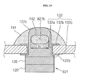
- the PCM 130 includes an insulation board 131, a printed circuit pattern 132, and circuit elements (not shown). In addition, the PCM 130 may further include a connector (not shown).
- the insulation board 131 has a via hole 133 passing through top and bottom surfaces thereof.
- the insulation board 131 is made of a resin-based material such as epoxy resin or bakelite.
- the insulation board 131 may include a plurality of compressed layers.
- the via hole 133 is formed to have a tetragonal plane, preferably a rectangular plane having a width-to-depth ratio.
- the via hole 133 is a portion into which the insertion portion 127 is inserted.
- the via hole 133 is formed to pass through top and bottom surfaces of the insulation board 131. In the illustrated embodiment, the via hole 133 has its width that is longer than its depth.
- the printed circuit pattern 132 may be formed on a surface of the insulation board 131 by, for example, plating.
- the printed circuit pattern 132 may be formed to have various patterns according to the design of the PCM 130.
- the printed circuit pattern 132 may be formed on both of the top and bottom surfaces of the insulation board 131.
- the printed circuit pattern 132 may also be formed on an intermediate layer of the insulation board 131.
- FIG. 3 illustrates an example printed circuit pattern formed around the via hole 133.
- the printed circuit pattern 132 includes an inner pattern 132a, an upper pattern 132b, and a lower pattern 132c.
- the inner pattern 132a is formed on the internal surface of the via hole 133.
- the upper pattern 132b is led to the inner pattern 132a and extends away from the inner pattern 132a on the top surface of the insulation board 131.
- the lower pattern 132c is led to the inner pattern 132a and extends away from the inner pattern 132a on the bottom surface of the insulation board 131.
- the inner pattern 132a, the upper pattern 132b, and the lower pattern 132c integrally cover the upper, middle and lower portions of the via hole 133, coupling forces between each of the inner pattern 132a, the upper pattern 132b and the lower pattern 132c, and the insulation board 131 are improved. Therefore, a coupling force between the solder portion 140 connected to the via hole patterns 132a and 132b and the PCM 130 is also improved.
- the circuit elements are placed on the insulation board 131 and are electrically connected to each other through the printed circuit pattern 132.
- the circuit elements measure voltages of the multi-cell module 110 and control charging/discharging of the multi-cell module 110 according to the charge/discharge state of the multi-cell 110. More specifically, the circuit elements include a charge field effect transistor (FET) (not shown), a discharge FET (not shown), a positive temperature coefficient (PTC) element (not shown), and a controller (not shown).
- FET charge field effect transistor
- PTC positive temperature coefficient
- the connector (not shown) is placed on the top surface of the insulation board 131 and is electrically connected to the printed circuit pattern 132.
- the connector may be electrically connected to a battery connection terminal of a portable electronic device.
- the connector is exposed to the outside of a case (not shown) surrounding the multi-cell module 110 and the PCM 130.
- the solder portion 140 includes a first solder portion 141 and a second solder portion 142.
- the solder portion 140 is formed by soldering the PCM 130 and the insertion portion 127.
- the first solder portion 141 is formed outside the fixing portion 127a, and the second solder portion 142 is formed in the gap 127b.
- the first solder portion 141 and the second solder portion 142 are integrally connected to increase a coupling force therebetween.
- the solder portion 140 Since the first solder portion 141 and the second solder portion 142 are integrally formed, the solder portion 140 has an increased coupling force compared to a case where only the first solder portion 141 is provided. Therefore, an amount of solder introduced into the solder portion 140 may be reduced.
- FIG. 8 is a vertical section view illustrating a portion of a battery pack according to another embodiment of the present invention, corresponding to FIG. 7 , in which a printed circuit module (PCM) and a conductive lead of a connection circuit board are connected to each other.
- PCM printed circuit module
- the battery pack according to the illustrated embodiment includes unit cells 111, a connection circuit board 120, a PCM 130 and a solder portion 140.
- unit cells 111, the connection circuit board 120, the PCM 130 and the solder portion 140 are the same as above with reference to FIG. 7 , functional elements that are the same as or similar to those shown in FIG. 7 are denoted by the same reference numerals, and detailed descriptions thereof will not be given.
- a gap 227b has a constant width, and, a depth Y2 ranging from either end of the insertion portion 227 to a bottom portion of the PCM 130, as shown in FIG. 7 .
- the depth Y2 may be set such that the gap 227b may not extend beyond the bottom portion of the PCM 130. If the gap 227b extends beyond a lower extension line (not shown) of the PCM 130, the solder inserted into the gap 227b may flow out.
- the gap 227b may be formed to have the maximum depth Y2 so as to increase coupling reliability of the first solder portion 141, the second solder portion 142 and the insertion portion 227 at the top portion of the PCM 130.
- a ratio of the area of the gap 227b to the area of insertion portion 227 of the conductive lead 321 is in a range of 29 to 74%.
- the area of the gap 227b is calculated based on the width X2 and depth Y2 of the internal space of the gap 227b. Assuming that the width X2 and depth Y2 of the gap 227b are 1.4 mm and 2.6 mm, respectively, the entire width L21 of the fixing portion 227a is 2 mm and an insertion height W1 is 2.45 mm, the area ratio may be calculated using the relationship (X2 ⁇ Y2)/(L2 ⁇ W2). In the illustrated embodiment, the area ratio is approximately 74%.
- a battery pack according to still another embodiment of the present invention will now be described.
- FIG. 9 is a vertical section view illustrating a portion of a battery pack according to still another embodiment of the present invention, in which a printed circuit module (PCM) 130 and a conductive lead 321 of a connection circuit board 120 are connected to each other.
- PCM printed circuit module
- the battery pack according to the illustrated embodiment includes unit cells 111, a connection circuit board 120, a PCM 130 and a solder portion 140.
- a plurality of gaps 327b are provided. Accordingly, in the following description, the battery pack according to the illustrated embodiment will be described with regard to the gaps 327b of the connection circuit board 120.
- FIG. 9 only the connection circuit board 120, the PCM 130 and the solder portion 140 are illustrated. Since the PCM 130 and the solder portion 140 are the same as above with reference to FIG. 1 to 7 , functional elements that are the same as or similar to those shown in FIG. 1 to 7 are denoted by the same reference numerals, and detailed descriptions thereof will not be given.
- the plurality of gaps 327b are provided to increase coupling reliability of the first solder portion 141, the second solder portion 142 and the insertion portion 127 at the top portion of the PCM 130.
- a ratio of the area of the gap 327b to the area of insertion portion 127 of the conductive lead 321 is in a range of 29 to 74%.
- a battery pack according to still another embodiment of the present invention will now be described.
- FIG. 10 is a vertical section view illustrating a portion of a battery pack according to still another embodiment of the present invention, in which a printed circuit module (PCM) 130 and a conductive lead 421 of a connection circuit board 120 are connected to each other.
- PCM printed circuit module
- the battery pack according to the illustrated embodiment includes unit cells 111, a connection circuit board 120, a PCM 130 and a solder portion 140.
- a gap 427b has a V-shape. Accordingly, in the following description, the battery pack according to the illustrated embodiment will be described with regard to the gap 427b of the connection circuit board 120.
- FIG. 10 only the connection circuit board 120, the PCM 130 and the solder portion 140 are illustrated.
- functional elements that are the same as or similar to those shown in FIG. 1 to 7 are denoted by the same reference numerals, and detailed descriptions thereof will not be given.
- the gap 427b is formed such that a width of its internal space gradually decreases toward the interior side of the conductive lead 421.
- the gap 427b is formed to range from the centre of its width to the top portion of the PCM 130 to be connected to the first solder portion 141, so that a contact area between the conductive lead 421 and the solder portion 140 may increase.
- the gap 427b is formed to have the minimum depth Y3. Since the conductive lead 421 has the gap 427b having a reduced depth, the strength of the conductive lead 421 may be comparatively increased.
- a ratio of the area of the gap 427b to the area of an insertion portion 127 of the conductive lead 421 is in a range of 29 to 74%. Since the gap 427b having the minimum depth Y3 is the same as described above with reference to FIG. 5 , functional elements that are the same as or similar to those of the previous embodiment are denoted by the same reference numerals, and detailed descriptions thereof will not be given. In the illustrated embodiment, the area ratio is approximately 29%.
- a battery pack according to still another embodiment of the present invention will now be described.
- FIG. 11 is a vertical section view illustrating a portion of a battery pack according to still another embodiment of the present invention, in which a printed circuit module (PCM) 130 and a conductive lead 521 of a connection circuit board 120 are connected to each other.
- PCM printed circuit module
- the battery pack according to the illustrated embodiment includes unit cells 111, a connection circuit board 120, a PCM 130 and a solder portion 140.
- a depth of a gap 527b may become maximized when the insertion portion 127 is inserted into a via hole 133.
- the maximum depth Y4 corresponds to a depth ranging up to a bottom portion of the PCM 130, as shown in FIG. 11 . If the gap 527b extends beyond a lower extension line (not shown) of the PCM 130, the solder inserted into the gap 527b may flow out.
- the gap 527b is formed to range from the center of its width to the bottom portion of the PCM 130 to be connected to the first solder portion 141, so that a contact area between the conductive lead 521 and the solder portion 140 may become maximized.
- a ratio of the area of the gap 527b to the area of an insertion portion 127 of the conductive lead 521 is in a range of 29 to 74%. Since the gap 527b having the maximum depth Y4 is similar to that described above with reference to FIG. 10 , functional elements that are the same as or similar to those of the previous embodiment are denoted by the same reference numerals, and detailed descriptions thereof will not be given. In the illustrated embodiment, the area ratio is approximately 29%. The area of the gap 527b is calculated based on the shape of the gap 527b, and a detailed explanation thereof will be omitted. In the illustrated embodiment, the area ratio may be approximately 74% or less.
- a battery pack according to still another embodiment of the present invention will now be described.
- FIG. 12 is a vertical section view illustrating a portion of a battery pack according to still another embodiment of the present invention, in which a printed circuit module (PCM) 130 and a conductive lead 621 of a connection circuit board 120 are connected to each other.
- PCM printed circuit module
- the battery pack according to the illustrated embodiment includes unit cells 111, a connection circuit board 120, a PCM 130 and a solder portion 140.
- the conductive lead 621 is distinguished from the conductive leads of the previous embodiments, in view of a configuration of a gap 627b. Accordingly, in the following description, the battery pack according to the illustrated embodiment will be described with regard to the gap 627b of the connection circuit board 120.
- FIG. 12 only the connection circuit board 120, the PCM 130 and the solder portion 140 are illustrated. Functional elements that are the same as or similar to those shown in FIG. 1 to 7 are denoted by the same reference numerals, and detailed descriptions thereof will not be given.
- the gap 627b may be formed at either side surface end of the fixing portion 127a.
- one or more of the gap 627b may be formed in one direction or opposite directions of the fixing portion 127a. Therefore, the second solder portion 142 formed in the gap 627b is connected to a first solder portion 141 so as to increase a contact area between the second solder portion 142 and the fixing portion 127a. Since the conductive lead 621 has the gaps 627b having reduced widths X3 and X4 and depths Y5 and Y6, the strength of the conductive lead 621 may be comparatively increased.
- a ratio of the area of the gap 627b to the area of an insertion portion 127 of the conductive lead 621 is in a range of 29 to 74%.
- the area of the gap 627b is obtained based on two widths X3 and X4 and depths Y5 and Y6 of the gap 627b.
- the sum of the two widths X3 and X4 of the gap 627b is smaller than the entire width of the insertion portion 127. For example, when the entire width of the insertion portion 127 is 4 mm, the sum of the two widths X3 and X4 of the gap 627b is 4 mm or less.
- the two widths X3 and X4 of the gap 627b may be different from each other.
- the area ratio may be calculated using the relationship (Minimum area of gap)/(Maximum area of insertion portion).
- the area may be calculated based on the shape of the gap 627b, and a detailed explanation thereof will be omitted.
- a battery pack according to still another embodiment of the present invention will now be described.
- FIG. 13 is a vertical section view illustrating a portion of a battery pack according to still another embodiment of the present invention, in which a printed circuit module (PCM) 130 and a conductive lead 721 of a connection circuit board 120 are connected to each other.
- PCM printed circuit module
- the battery pack according to the illustrated embodiment includes unit cells 111, a connection circuit board 120, a PCM 130 and a solder portion 140.
- the conductive lead 721 is distinguished from the conductive leads of the previous embodiments, in view of a configuration of a gap 727b. That is to say, the gap 727b has widths X5 and X6, and depths Y7 and Y8, which area symmetrical to each other, but aspects of the invention are not limited to the illustrated embodiment in view of the length and number the gap 727b.
- the depths Y7 and Y8 of the gap 727b may not extend beyond the bottom portion of the PCM 130. If the gap 727b extends beyond a lower extension line (not shown) of the PCM 130, the solder inserted into the gap 727b may flow out.
- a ratio of the area of the gap 727b to the area of an insertion portion 127 of the conductive lead 721 is in a range of 29 to 74%.
- the area of the gap 727b is obtained based on two widths X5 and X6 and depths Y7 and Y8 of the gap 727b.
- the sum of the two widths X5 and X6 of the gap 727b is smaller than the entire width of the insertion portion 127. For example, when the entire width of the insertion portion 127 is 4 mm, the sum of the two widths X5 and X6 of the gap 727b is 4 mm or less.
- the area ratio may be calculated using the relationship (Minimum area of gap)/(Maximum area of insertion portion).
- the area may be calculated based on the shape of the gap 727b, and a detailed explanation thereof will be omitted.
- a battery pack according to still another embodiment of the present invention will now be described.
- FIG. 14 is a vertical section view illustrating a portion of a battery pack according to still another embodiment of the present invention, in which a printed circuit module (PCM) 130 and a conductive lead 821 of a connection circuit board 120 are connected to each other.
- PCM printed circuit module
- the battery pack according to the illustrated embodiment includes unit cells 111, a connection circuit board 120, a PCM 130 and a solder portion 140.
- the conductive lead 821 is distinguished from the conductive leads of the previous embodiments, in view of a configuration of a gap 827b. Accordingly, in the following description, the battery pack according to the illustrated embodiment will be described with regard to the gap 827b of the connection circuit board 120.
- FIG. 14 only the conductive lead 821, the PCM 130 and the solder portion 140 are illustrated. Functional elements that are the same as or similar to those shown in FIG. 1 to 7 are denoted by the same reference numerals, and detailed descriptions thereof will not be given.
- the gap 827b may be formed on a fixing portion 127a in the form of a through groove of a circular shape.
- the gap 827b may be formed in a circular or oval shape.
- the conductive lead 821 is formed to have the minimum area of the gap 821b. Since the conductive lead 821 occupies the minimum area of the gap 821 a, the strength of the conductive lead 821 may be comparatively increased.
- a ratio of the area of the gap 827b to the area of an insertion portion 127 of the conductive lead 821 is in a range of 29 to 74%.
- a width X7 of the gap 827b formed at either side surface end of the is smaller than the gap 827b is smaller than the entire width of the insertion portion 127.
- the area ratio may be calculated using the relationship (Minimum area of gap)/(Maximum area of insertion portion).
- the area may be calculated based on the shape of the gap 827b, and a detailed explanation thereof will be omitted. In the illustrated embodiment, the area ratio is approximately 29% or greater.
- a battery pack according to still another embodiment of the present invention will now be described.
- FIG. 15 is a vertical section view illustrating a portion of a battery pack according to still another embodiment of the present invention, in which a printed circuit module (PCM) 130 and a conductive lead 921 of a connection circuit board 120 are connected to each other.
- PCM printed circuit module
- the battery pack according to the illustrated embodiment includes unit cells 111, a connection circuit board 120, a PCM 130 and a solder portion 140.
- the conductive lead 921 is distinguished from the conductive leads of the previous embodiments, in view of a configuration of a gap 927b. Accordingly, in the following description, the battery pack according to the illustrated embodiment will be described with regard to the gap 927b of the connection circuit board 120.
- FIG. 15 only the connection circuit board 120, the PCM 130 and the solder portion 140 are illustrated. Functional elements that are the same as or similar to those shown in FIG. 1 to 7 are denoted by the same reference numerals, and detailed descriptions thereof will not be given.
- the gap 927b may be formed on a fixing portion 127a so as to have various numbers and sizes.
- the gap 927b is formed to have the maximum area.
- the gap 927b may be formed such that an outer circumferential surface of the gap 927b does not extend beyond a lower extension line (not shown) of the PCM 130. If the outer circumferential surface of the gap 927b extends beyond the lower extension line of the PCM 130, the solder inserted into the gap 727b may flow out.
- a ratio of the area of the gap 927b to the area of an insertion portion 127 of the conductive lead 921 is in a range of 29 to 74%.
- a width X8 of the gap 927b formed at either side surface end of the is smaller than the gap 927b is preferably smaller than the entire width of the insertion portion 127, and a depth Y9 of the gap 927b preferably smaller than a height of the fixing portion 127a.
- the area ratio may be calculated using the relationship (Minimum area of gap)/(Maximum area of insertion portion).
- the area may be calculated based on the shape of the gap 927b, and a detailed explanation thereof will be omitted. In the illustrated embodiment, the area ratio is approximately 74% or less.
Landscapes
- Engineering & Computer Science (AREA)
- Chemical & Material Sciences (AREA)
- Chemical Kinetics & Catalysis (AREA)
- Electrochemistry (AREA)
- General Chemical & Material Sciences (AREA)
- Manufacturing & Machinery (AREA)
- Microelectronics & Electronic Packaging (AREA)
- Battery Mounting, Suspending (AREA)
- Connection Of Batteries Or Terminals (AREA)
Abstract
Description
- The present invention relates to a battery pack. A battery pack includes a plurality of battery cells, also referred to herein as a multi-cell module, and a protection circuit module (PCM).
- The unit cells making up the multi-cell module include rechargeable bare cells.
- The PCM includes a field effect transistor (FET) as a switching element that blocks current, a resistor, capacitor, etc. The PCM controls charging/discharging operations of the unit cell, and prevents over-charge, over-discharge, over-current, etc.
- The PCM is electrically connected to the unit cell by soldering.
- However, in order to increase a coupling force between the PCM and the unit cell, an amount of solder used may increase. In this case, a height of a solder portion may increase. In addition, when the amount of solder used increases and the height of the solder portion is increased, a distance between the PCM and a case is reduced. Accordingly, a space for mounting other elements in the PCM is reduced, that is, distances between each of the elements become smaller, which may make the assembly process complicated.
- Aspects of the present invention provide a battery pack having improved product reliability by reducing a height of a solder portion provided when a multi-cell module is connected to a protection circuit module (PCM) in series or parallel.
- Aspects of the present invention also provide a battery pack having improved reliability in connecting a conductive lead to the PCM by increasing a contact area of the conductive lead of a connection circuit board and a solder portion when soldering the connection circuit board and the PCM.
- According to an aspect of the invention, there is provided a battery pack comprising one or more battery cells, a connecting circuit board connected to the one or more battery cells, the circuit board comprising one or more connectors for connecting the one or more battery cells to a protection circuit module PCM, the PCM having a through hole for receiving a corresponding one of the connectors, wherein each of the one or more connectors comprises a base portion and a receiving portion for holding solder, wherein the base portion is arranged to abut the PCM so as to seal one side of the through hole to prevent solder flowing through the through hole.
- The receiving portion may comprise first and second protruding portions extending from the base portion and arranged to pass through the through hole in the PCM, the protruding portions being separated from one another by a gap and outside edges of the first and second protruding portions being rounded, wherein when the protruding portions are soldered to the PCM, the gap is arranged to receive solder.
- The gap may have a substantially rectangular profile or may taper towards a bottom of the gap.
- The battery pack may comprise further projections arranged between the first and second projections, such that the connector comprises three or more projections with gaps between them.
- The first and second projections may be joined at a top portion distal from the base portion such that the gap is enclosed by the projections. The gap may have a substantially circular or oval profile.
- The PCM may comprise a substantially planar PCM circuit board and a bottom of the gap may be arranged to be in line with a top or a bottom surface of the PCM circuit board.
- The battery pack may further comprise a protruding portion extending from the base portion and arranged to pass through the through hole in the PCM and a rounded cap at the top of the protruding portion, the cap having overhanging portions that define a gap between the overhanging portions and the base portion, wherein the gap comprises the receiving portion that is arranged to receive solder when the connector is soldered to the PCM.
- The width of the rounded cap including the overhanging portions may not be greater than the width of the through hole.
- The PCM may comprise a substantially planar PCM circuit board and a top of the base portion may be arranged to be in line with a top or a bottom surface of the PCM circuit board.
- The ratio of the cross-sectional area of the gap to the cross-sectional area of the portion of the connector inserted into the through hole may be between 29% and 74%.
- The PCM may comprise a substantially planar PCM circuit board and the connector may comprise a stepped portion arranged to be in contact with a first side of the PCM circuit board opposite the side at which the first and second projections protrude.
- The connector may comprise an extension portion extending from the connecting circuit board and parallel to an insertion portion of the connector that is inserted into the through hole, the connector further comprising a bent portion between the extension portion and the insertion portion.
- The PCM may include a substantially planar circuit board and a printed circuit pattern on the circuit board, wherein the printed circuit pattern is formed around the through hole and the connector is soldered to an upper portion of the printed circuit pattern.
- The battery pack may comprise a plurality of battery cells, wherein each of the battery cells has a protective circuit element and first and second electrode tabs, the second electrode tab being connected to one end of the protective circuit element, the first electrode tab and a lead from the other end of the protective circuit element being connected to the connecting circuit board. As described above, in the connection circuit board of the present invention and the battery pack including the same, when a multi-cell module is connected to a printed circuit module in series or parallel, a height of a solder portion can be reduced.
- In addition, in the connection circuit board of the present invention and the battery pack including the same, coupling reliability can be improved by increasing a contact area of a conductive lead and a solder portion of the connection circuit board.
- Embodiments of the invention will now be described, by way of example, with reference to the accompanying drawings, in which:
-
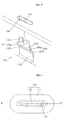
FIG. 1 is a perspective view of a battery pack according to an embodiment of the present invention; -
FIG. 2 is an enlarged perspective view of a portion A ofFIG. 1 ; -
FIG. 3 is a partially perspective view of a unit cell constituting the battery pack shown inFIG. 1 ; -
FIG. 4 is a partially perspective view illustrating a connection relationship between the unit cell shown inFIG. 3 and a connection circuit board; -
FIG. 5 is a perspective view illustrating a conductive lead and a via hole shown in -
FIG. 1 separated from each other; -
FIG. 6 is a front view of a soldering connection ofFIG. 5 ; -
FIG. 7 is a vertical section view taken along the line B-B' ofFIG. 6 ; -
FIG. 8 is a vertical section view illustrating a portion of a battery pack according to another embodiment of the present invention; -
FIG. 9 is a vertical section view illustrating a portion of a battery pack according to still another embodiment of the present invention; -
FIG. 10 is a vertical section view illustrating a portion of a battery pack according to still another embodiment of the present invention; -
FIG. 11 is a vertical section view illustrating a portion of a battery pack according to still another embodiment of the present invention; -
FIG. 12 is a vertical section view illustrating a portion of a battery pack according to still another embodiment of the present invention; -
FIG. 13 is a vertical section view illustrating a portion of a battery pack according to still another embodiment of the present invention; -
FIG. 14 is a vertical section view illustrating a portion of a battery pack according to still another embodiment of the present invention; and -
FIG. 15 is a vertical section view illustrating a portion of a battery pack according to still another embodiment of the present invention. - Referring to
FIGS. 1 to 7 , thebattery pack 100 according to an embodiment of the present invention includes amulti-cell module 110, aconnection circuit board 120, a protection circuit module (PCM) 130, and asolder portion 140. - The
battery pack 100 has themulti-cell module 110 and theprotection circuit module 130 electrically connected to each other. In themulti-cell module 110, a negative electrode tab or a positive electrode tab of each cell is connected to theconnection circuit board 120. Theconnection circuit board 120 is electrically connected to the PCM 130 and is fixed by thesolder portion 140. - The
multi-cell module 110 includes a plurality ofunit cells 111. Themulti-cell module 110 is configured such that theunit cells 111 are connected in series or parallel to each other to provide a positive electrode and a negative electrode. - Each of the
unit cells 111 includes abare cell 112, aprotective element 115, and acover 119. Thebare cell 112 includes an electrode assembly (not shown), afirst electrode tab 113, and asecond electrode tab 114. - The
bare cell 112 accommodates the electrode assembly (not shown) and electrolyte. Thebare cell 112 may be formed to have a shape that is the same as or similar to that of a general pouch-type battery, and a detailed description thereof will not be given. - The electrode assembly is configured by a negative electrode plate (not shown), a positive electrode plate (not shown), and a separator (not shown) sequentially stacked and wound.
- The
first electrode tab 113 and thesecond electrode tab 114 have different polarities from each other. That is to say, thefirst electrode tab 113 is electrically connected to the positive electrode plate of the electrode assembly, and thesecond electrode tab 114 is electrically connected to the negative electrode plate of the electrode assembly. - The
protective element 115 includes afunctional element 116, afirst lead 116a, asecond lead 116b, and a protectiveelement lead tab 117. - The
functional element 116 is, for example, a positive temperature coefficient (PTC) element. When the temperature of theunit cell 111 rises, internal resistance increases and blocks current. - The
first lead 116a is electrically connected to thesecond electrode tab 114. Thesecond lead 116b is electrically connected to the protectiveelement lead tab 117. - The
element lead tab 117 is plate-shaped and is made of the same material as that of thesecond electrode tab 114, or an electrically conductive material. - The
cover 119 includes acover body 119a and acover fixing portion 119b. - In the
cover 119, theprotective element 115 is positioned at a sealingpart 111a of theunit cell 111 and an upper portion of theunit cells 111 is subjected to a finishing process. Thecover body 119a is rotated about a plane close to the sealingpart 111a of theunit cell 111 and is coupled to thecover fixing portion 119b. Here, when thecover body 119a is coupled to thecover fixing portion 119b, thesecond electrode tab 114 connected to thefirst lead 116 of theprotective element 115 is bent in a U-shape. - The
cover body 119a is formed to accommodate theprotective element 115 inside. In addition, thecover body 119a includes afirst extraction hole 119c and asecond extraction hole 119d formed at a location close to the sealingpart 111a of thefirst extraction hole 119c, thefirst extraction hole 119c through which thefirst electrode tab 113 is drawn out, and thesecond extraction hole 119d through which the protectiveelement lead tab 117 is drawn out.Hole 119e denotes a hole for welding thesecond electrode tab 114 and thefirst lead 116 to each other. - The
cover fixing portion 119b is formed on upper portions of theunit cells 111. Thecover body 119a and thecover fixing portion 119b are coupled to each other and the upper portions of theunit cells 111 are finished. - The
connection circuit board 120 has a plurality of wire patterns (not shown) formed therein, and aconductive lead 121 drawn out outwardly. Theconductive lead 121 may includes a multiple number ofconductive leads connection circuit board 120. Although not specifically shown, theconnection circuit board 120 may include wire patterns (not shown) therein, like in a general flexible printed circuit board (FPCB). - The
connection circuit board 120 is electrically connected to thefirst electrode tab 113 and the protectiveelement lead tab 117 drawn out from theunit cell 111. - The
conductive lead 121 is shaped of a plate made of a material having electrical conductivity, and includes aninsertion portion 127, abent portion 128b, and an extendingportion 129. Theconductive lead 121 is electrically connected to thePCM 130. - The
insertion portion 127 includes a fixingportion 127a. - The fixing
portion 127a comprises first and second projections having roundedoutside edges 127c, the projections being separated from one another by agap 127b, which acts as a receiving portion for thesolder 140. Thegap 127b may be rectangular, for example having a depth Y1 and width X1. The bottom of thegap 127b is in line with an upper surface of thePCB 130 when theinsertion portion 127 has been inserted into a through hole in thePCB 130. - The
gap 127b increases a contact area of theinsertion portion 127 and thesolder portion 140, thereby improving a coupling force therebetween. - The
gap 127b may have the depth Y1 to have an increased strength. Here, a ratio of the cross-sectional area of thegap 127b to the cross-sectional area of theinsertion portion 127 of theconductive lead 121 is in the range of 29 to 74%. - The area of the
gap 127b is calculated based on its width X1 and depth Y1. - Assuming that the width X1 and depth Y1 of the
gap 127b are 1 mm and 2.4 mm, respectively, the entire width L1 of the fixingportion 127a is 3 mm and an insertion height W1 is 2.75 mm, the area ratio may be calculated using the relationship (X1×Y1)/(L1×W1). In the illustrated embodiment, the area ratio is approximately 29%. - In addition, the rounded
outside edges 127c, also referred to as a slanting portion, are formed by rounding both ends of the fixingportion 127a. The rounded surfaces of the slantingportion 127c may reduce a height of thesolder portion 140 when thePCB 130 and the fixingportion 127a are coupled to each other. - Further, the
insertion portion 127 has a steppedportion 127d so as to contact a bottom portion of thePCB 130. The steppedportion 127d is formed to have a width greater than the entire width of theinsertion portion 127 at a location where it is formed to have a thickness equal to or greater than a thickness of thePCB 130 at both ends of theinsertion portion 127. - The
bent portion 128b is bent and extends from the steppedportion 127d via astraight portion 128a. The bending range is in a range of approximately 30 to 90 degrees from the direction in which theinsertion portion 127 is inserted into the printedcircuit module 130. Here, thebent portion 128b may vary so as to facilitate an assembling work of the battery pack. - In another embodiment, the
portion 128a may also be bent in a similar way to thebent portion 128b. - The
bent portion 128b is bent to prevent thesolder portion 140 introduced from an upper portion of thePCB 130 from flowing downward. - The extending
portion 129 is formed to be led to thebent portion 128b. When theinsertion portion 127 is inserted into thePCM 130, the extendingportion 129 facilitates an assembling work by upwardly or downwardly moving in view of theconnection circuit board 120. - The
PCM 130 includes aninsulation board 131, a printedcircuit pattern 132, and circuit elements (not shown). In addition, thePCM 130 may further include a connector (not shown). - The
insulation board 131 has a viahole 133 passing through top and bottom surfaces thereof. Theinsulation board 131 is made of a resin-based material such as epoxy resin or bakelite. Theinsulation board 131 may include a plurality of compressed layers. - The via
hole 133 is formed to have a tetragonal plane, preferably a rectangular plane having a width-to-depth ratio. The viahole 133 is a portion into which theinsertion portion 127 is inserted. The viahole 133 is formed to pass through top and bottom surfaces of theinsulation board 131. In the illustrated embodiment, the viahole 133 has its width that is longer than its depth. - The printed
circuit pattern 132 may be formed on a surface of theinsulation board 131 by, for example, plating. The printedcircuit pattern 132 may be formed to have various patterns according to the design of thePCM 130. In addition, the printedcircuit pattern 132 may be formed on both of the top and bottom surfaces of theinsulation board 131. The printedcircuit pattern 132 may also be formed on an intermediate layer of theinsulation board 131.FIG. 3 illustrates an example printed circuit pattern formed around the viahole 133. - The printed
circuit pattern 132 includes aninner pattern 132a, anupper pattern 132b, and alower pattern 132c. - The
inner pattern 132a is formed on the internal surface of the viahole 133. - The
upper pattern 132b is led to theinner pattern 132a and extends away from theinner pattern 132a on the top surface of theinsulation board 131. - The
lower pattern 132c is led to theinner pattern 132a and extends away from theinner pattern 132a on the bottom surface of theinsulation board 131. - Since the
inner pattern 132a, theupper pattern 132b, and thelower pattern 132c integrally cover the upper, middle and lower portions of the viahole 133, coupling forces between each of theinner pattern 132a, theupper pattern 132b and thelower pattern 132c, and theinsulation board 131 are improved. Therefore, a coupling force between thesolder portion 140 connected to the viahole patterns PCM 130 is also improved. - The circuit elements (not shown) are placed on the
insulation board 131 and are electrically connected to each other through the printedcircuit pattern 132. The circuit elements measure voltages of themulti-cell module 110 and control charging/discharging of themulti-cell module 110 according to the charge/discharge state of the multi-cell 110. More specifically, the circuit elements include a charge field effect transistor (FET) (not shown), a discharge FET (not shown), a positive temperature coefficient (PTC) element (not shown), and a controller (not shown). - The connector (not shown) is placed on the top surface of the
insulation board 131 and is electrically connected to the printedcircuit pattern 132. In addition, the connector may be electrically connected to a battery connection terminal of a portable electronic device. In this case, the connector is exposed to the outside of a case (not shown) surrounding themulti-cell module 110 and thePCM 130. - Referring to
FIG. 6 , thesolder portion 140 includes afirst solder portion 141 and asecond solder portion 142. Thesolder portion 140 is formed by soldering thePCM 130 and theinsertion portion 127. Thefirst solder portion 141 is formed outside the fixingportion 127a, and thesecond solder portion 142 is formed in thegap 127b. Here, thefirst solder portion 141 and thesecond solder portion 142 are integrally connected to increase a coupling force therebetween. - Since the
first solder portion 141 and thesecond solder portion 142 are integrally formed, thesolder portion 140 has an increased coupling force compared to a case where only thefirst solder portion 141 is provided. Therefore, an amount of solder introduced into thesolder portion 140 may be reduced. - Next, a battery pack according to another embodiment of the present invention will be described.
-
FIG. 8 is a vertical section view illustrating a portion of a battery pack according to another embodiment of the present invention, corresponding toFIG. 7 , in which a printed circuit module (PCM) and a conductive lead of a connection circuit board are connected to each other. - The battery pack according to the illustrated embodiment includes
unit cells 111, aconnection circuit board 120, aPCM 130 and asolder portion 140. In the illustrated embodiment, since theunit cells 111, theconnection circuit board 120, thePCM 130 and thesolder portion 140 are the same as above with reference toFIG. 7 , functional elements that are the same as or similar to those shown inFIG. 7 are denoted by the same reference numerals, and detailed descriptions thereof will not be given. - In the
conductive lead 221 according to the illustrated embodiment, agap 227b has a constant width, and, a depth Y2 ranging from either end of the insertion portion 227 to a bottom portion of thePCM 130, as shown inFIG. 7 . Here, the depth Y2 may be set such that thegap 227b may not extend beyond the bottom portion of thePCM 130. If thegap 227b extends beyond a lower extension line (not shown) of thePCM 130, the solder inserted into thegap 227b may flow out. - The
gap 227b may be formed to have the maximum depth Y2 so as to increase coupling reliability of thefirst solder portion 141, thesecond solder portion 142 and the insertion portion 227 at the top portion of thePCM 130. Here, a ratio of the area of thegap 227b to the area of insertion portion 227 of theconductive lead 321 is in a range of 29 to 74%. - The area of the
gap 227b is calculated based on the width X2 and depth Y2 of the internal space of thegap 227b. Assuming that the width X2 and depth Y2 of thegap 227b are 1.4 mm and 2.6 mm, respectively, the entire width L21 of the fixing portion 227a is 2 mm and an insertion height W1 is 2.45 mm, the area ratio may be calculated using the relationship (X2×Y2)/(L2×W2). In the illustrated embodiment, the area ratio is approximately 74%. - A battery pack according to still another embodiment of the present invention will now be described.
-
FIG. 9 is a vertical section view illustrating a portion of a battery pack according to still another embodiment of the present invention, in which a printed circuit module (PCM) 130 and aconductive lead 321 of aconnection circuit board 120 are connected to each other. - The battery pack according to the illustrated embodiment includes
unit cells 111, aconnection circuit board 120, aPCM 130 and asolder portion 140. - In the
conductive lead 321 according to the illustrated embodiment, a plurality ofgaps 327b are provided. Accordingly, in the following description, the battery pack according to the illustrated embodiment will be described with regard to thegaps 327b of theconnection circuit board 120. InFIG. 9 , only theconnection circuit board 120, thePCM 130 and thesolder portion 140 are illustrated. Since thePCM 130 and thesolder portion 140 are the same as above with reference toFIG. 1 to 7 , functional elements that are the same as or similar to those shown inFIG. 1 to 7 are denoted by the same reference numerals, and detailed descriptions thereof will not be given. - In the
conductive lead 321 according to the illustrated embodiment, the plurality ofgaps 327b are provided to increase coupling reliability of thefirst solder portion 141, thesecond solder portion 142 and theinsertion portion 127 at the top portion of thePCM 130. Here, a ratio of the area of thegap 327b to the area ofinsertion portion 127 of theconductive lead 321 is in a range of 29 to 74%. - A battery pack according to still another embodiment of the present invention will now be described.
-
FIG. 10 is a vertical section view illustrating a portion of a battery pack according to still another embodiment of the present invention, in which a printed circuit module (PCM) 130 and aconductive lead 421 of aconnection circuit board 120 are connected to each other. - The battery pack according to the illustrated embodiment includes
unit cells 111, aconnection circuit board 120, aPCM 130 and asolder portion 140. - In the
conductive lead 421 according to the illustrated embodiment, agap 427b has a V-shape. Accordingly, in the following description, the battery pack according to the illustrated embodiment will be described with regard to thegap 427b of theconnection circuit board 120. InFIG. 10 , only theconnection circuit board 120, thePCM 130 and thesolder portion 140 are illustrated. In addition, functional elements that are the same as or similar to those shown inFIG. 1 to 7 are denoted by the same reference numerals, and detailed descriptions thereof will not be given. - The
gap 427b is formed such that a width of its internal space gradually decreases toward the interior side of theconductive lead 421. Thegap 427b is formed to range from the centre of its width to the top portion of thePCM 130 to be connected to thefirst solder portion 141, so that a contact area between theconductive lead 421 and thesolder portion 140 may increase. - Therefore, in order to increase the reliability of coupling the
connection circuit board 120 with thePCM 130, thegap 427b is formed to have the minimum depth Y3. Since theconductive lead 421 has thegap 427b having a reduced depth, the strength of theconductive lead 421 may be comparatively increased. - Here, a ratio of the area of the
gap 427b to the area of aninsertion portion 127 of theconductive lead 421 is in a range of 29 to 74%. Since thegap 427b having the minimum depth Y3 is the same as described above with reference toFIG. 5 , functional elements that are the same as or similar to those of the previous embodiment are denoted by the same reference numerals, and detailed descriptions thereof will not be given. In the illustrated embodiment, the area ratio is approximately 29%. - A battery pack according to still another embodiment of the present invention will now be described.
-
FIG. 11 is a vertical section view illustrating a portion of a battery pack according to still another embodiment of the present invention, in which a printed circuit module (PCM) 130 and aconductive lead 521 of aconnection circuit board 120 are connected to each other. - The battery pack according to the illustrated embodiment includes
unit cells 111, aconnection circuit board 120, aPCM 130 and asolder portion 140. - A depth of a
gap 527b according to the illustrated embodiment may become maximized when theinsertion portion 127 is inserted into a viahole 133. Here, the maximum depth Y4 corresponds to a depth ranging up to a bottom portion of thePCM 130, as shown inFIG. 11 . If thegap 527b extends beyond a lower extension line (not shown) of thePCM 130, the solder inserted into thegap 527b may flow out. - The
gap 527b is formed to range from the center of its width to the bottom portion of thePCM 130 to be connected to thefirst solder portion 141, so that a contact area between theconductive lead 521 and thesolder portion 140 may become maximized. - Here, a ratio of the area of the
gap 527b to the area of aninsertion portion 127 of theconductive lead 521 is in a range of 29 to 74%. Since thegap 527b having the maximum depth Y4 is similar to that described above with reference toFIG. 10 , functional elements that are the same as or similar to those of the previous embodiment are denoted by the same reference numerals, and detailed descriptions thereof will not be given. In the illustrated embodiment, the area ratio is approximately 29%. The area of thegap 527b is calculated based on the shape of thegap 527b, and a detailed explanation thereof will be omitted. In the illustrated embodiment, the area ratio may be approximately 74% or less. - A battery pack according to still another embodiment of the present invention will now be described.
-
FIG. 12 is a vertical section view illustrating a portion of a battery pack according to still another embodiment of the present invention, in which a printed circuit module (PCM) 130 and aconductive lead 621 of aconnection circuit board 120 are connected to each other. - The battery pack according to the illustrated embodiment includes
unit cells 111, aconnection circuit board 120, aPCM 130 and asolder portion 140. - Referring to
FIG. 12 , theconductive lead 621 is distinguished from the conductive leads of the previous embodiments, in view of a configuration of agap 627b. Accordingly, in the following description, the battery pack according to the illustrated embodiment will be described with regard to thegap 627b of theconnection circuit board 120. InFIG. 12 , only theconnection circuit board 120, thePCM 130 and thesolder portion 140 are illustrated. Functional elements that are the same as or similar to those shown inFIG. 1 to 7 are denoted by the same reference numerals, and detailed descriptions thereof will not be given. - The
gap 627b may be formed at either side surface end of the fixingportion 127a. Here, one or more of thegap 627b may be formed in one direction or opposite directions of the fixingportion 127a. Therefore, thesecond solder portion 142 formed in thegap 627b is connected to afirst solder portion 141 so as to increase a contact area between thesecond solder portion 142 and the fixingportion 127a. Since theconductive lead 621 has thegaps 627b having reduced widths X3 and X4 and depths Y5 and Y6, the strength of theconductive lead 621 may be comparatively increased. - Here, a ratio of the area of the
gap 627b to the area of aninsertion portion 127 of theconductive lead 621 is in a range of 29 to 74%. - The area of the
gap 627b is obtained based on two widths X3 and X4 and depths Y5 and Y6 of thegap 627b. The sum of the two widths X3 and X4 of thegap 627b is smaller than the entire width of theinsertion portion 127. For example, when the entire width of theinsertion portion 127 is 4 mm, the sum of the two widths X3 and X4 of thegap 627b is 4 mm or less. - Alternatively, the two widths X3 and X4 of the
gap 627b may be different from each other. - In the illustrated embodiment, the area ratio may be calculated using the relationship (Minimum area of gap)/(Maximum area of insertion portion). The area may be calculated based on the shape of the
gap 627b, and a detailed explanation thereof will be omitted. - A battery pack according to still another embodiment of the present invention will now be described.
-
FIG. 13 is a vertical section view illustrating a portion of a battery pack according to still another embodiment of the present invention, in which a printed circuit module (PCM) 130 and aconductive lead 721 of aconnection circuit board 120 are connected to each other. - The battery pack according to the illustrated embodiment includes
unit cells 111, aconnection circuit board 120, aPCM 130 and asolder portion 140. - Referring to
FIG. 13 , theconductive lead 721 is distinguished from the conductive leads of the previous embodiments, in view of a configuration of agap 727b. That is to say, thegap 727b has widths X5 and X6, and depths Y7 and Y8, which area symmetrical to each other, but aspects of the invention are not limited to the illustrated embodiment in view of the length and number thegap 727b. - As shown in
FIG. 13 , the depths Y7 and Y8 of thegap 727b may not extend beyond the bottom portion of thePCM 130. If thegap 727b extends beyond a lower extension line (not shown) of thePCM 130, the solder inserted into thegap 727b may flow out. - Here, a ratio of the area of the
gap 727b to the area of aninsertion portion 127 of theconductive lead 721 is in a range of 29 to 74%. - The area of the
gap 727b is obtained based on two widths X5 and X6 and depths Y7 and Y8 of thegap 727b. The sum of the two widths X5 and X6 of thegap 727b is smaller than the entire width of theinsertion portion 127. For example, when the entire width of theinsertion portion 127 is 4 mm, the sum of the two widths X5 and X6 of thegap 727b is 4 mm or less. - In the illustrated embodiment, the area ratio may be calculated using the relationship (Minimum area of gap)/(Maximum area of insertion portion). The area may be calculated based on the shape of the
gap 727b, and a detailed explanation thereof will be omitted. - A battery pack according to still another embodiment of the present invention will now be described.
-
FIG. 14 is a vertical section view illustrating a portion of a battery pack according to still another embodiment of the present invention, in which a printed circuit module (PCM) 130 and aconductive lead 821 of aconnection circuit board 120 are connected to each other. - The battery pack according to the illustrated embodiment includes
unit cells 111, aconnection circuit board 120, aPCM 130 and asolder portion 140. - Referring to
FIG. 14 , theconductive lead 821 is distinguished from the conductive leads of the previous embodiments, in view of a configuration of agap 827b. Accordingly, in the following description, the battery pack according to the illustrated embodiment will be described with regard to thegap 827b of theconnection circuit board 120. InFIG. 14 , only theconductive lead 821, thePCM 130 and thesolder portion 140 are illustrated. Functional elements that are the same as or similar to those shown inFIG. 1 to 7 are denoted by the same reference numerals, and detailed descriptions thereof will not be given. - In the illustrated embodiment, the
gap 827b may be formed on a fixingportion 127a in the form of a through groove of a circular shape. Thegap 827b may be formed in a circular or oval shape. Theconductive lead 821 is formed to have the minimum area of the gap 821b. Since theconductive lead 821 occupies the minimum area of the gap 821 a, the strength of theconductive lead 821 may be comparatively increased. - Here, a ratio of the area of the
gap 827b to the area of aninsertion portion 127 of theconductive lead 821 is in a range of 29 to 74%. - With respect to the area of the internal space of the
gap 827b, a width X7 of thegap 827b formed at either side surface end of the is smaller than thegap 827b is smaller than the entire width of theinsertion portion 127. - In the illustrated embodiment, the area ratio may be calculated using the relationship (Minimum area of gap)/(Maximum area of insertion portion). The area may be calculated based on the shape of the
gap 827b, and a detailed explanation thereof will be omitted. In the illustrated embodiment, the area ratio is approximately 29% or greater. - A battery pack according to still another embodiment of the present invention will now be described.
-
FIG. 15 is a vertical section view illustrating a portion of a battery pack according to still another embodiment of the present invention, in which a printed circuit module (PCM) 130 and aconductive lead 921 of aconnection circuit board 120 are connected to each other. - The battery pack according to the illustrated embodiment includes
unit cells 111, aconnection circuit board 120, aPCM 130 and asolder portion 140. - Referring to
FIG. 15 , theconductive lead 921 is distinguished from the conductive leads of the previous embodiments, in view of a configuration of agap 927b. Accordingly, in the following description, the battery pack according to the illustrated embodiment will be described with regard to thegap 927b of theconnection circuit board 120. InFIG. 15 , only theconnection circuit board 120, thePCM 130 and thesolder portion 140 are illustrated. Functional elements that are the same as or similar to those shown inFIG. 1 to 7 are denoted by the same reference numerals, and detailed descriptions thereof will not be given. - In modifications of the illustrated embodiment, the
gap 927b may be formed on a fixingportion 127a so as to have various numbers and sizes. Here, thegap 927b is formed to have the maximum area. In addition, thegap 927b may be formed such that an outer circumferential surface of thegap 927b does not extend beyond a lower extension line (not shown) of thePCM 130. If the outer circumferential surface of thegap 927b extends beyond the lower extension line of thePCM 130, the solder inserted into thegap 727b may flow out. - Here, a ratio of the area of the
gap 927b to the area of aninsertion portion 127 of theconductive lead 921 is in a range of 29 to 74%. - With respect to the area of the internal space of the
gap 927b, a width X8 of thegap 927b formed at either side surface end of the is smaller than thegap 927b is preferably smaller than the entire width of theinsertion portion 127, and a depth Y9 of thegap 927b preferably smaller than a height of the fixingportion 127a. - In the illustrated embodiment, the area ratio may be calculated using the relationship (Minimum area of gap)/(Maximum area of insertion portion). The area may be calculated based on the shape of the
gap 927b, and a detailed explanation thereof will be omitted. In the illustrated embodiment, the area ratio is approximately 74% or less. - Although the present invention has been described with reference to the preferred examples, the foregoing disclosure should be interpreted as illustrative only and it should be understood that various modifications and variations can be easily made by those skilled in the art without departing from the scope of the invention as defined in the appended claims.
Claims (15)
- A battery pack comprising:one or more battery cells (111);a connecting circuit board (120) connected to the one or more battery cells, the circuit board comprising one or more connectors for connecting the one or more battery cells to a protection circuit module PCM (130), the PCM having a through hole (133) for receiving a corresponding one of the connectors;wherein each of the one or more connectors comprises a base portion and a receiving portion (127b, 227b, 327b, 427b, 527b, 627b, 727b, 827b, 927b) for holding solder, wherein the base portion is arranged to abut the PCM so as to seal one side of the through hole to prevent solder flowing through the through hole.
- The battery pack of claim 1, wherein the receiving portion comprises first and second protruding portions (127a) extending from the base portion and arranged to pass through the through hole in the PCM (130), the protruding portions being separated from one another by a gap (127b, 227b, 327b, 427b, 527b, 827b, 927b) and outside edges (127c) of the first and second protruding portions being rounded, wherein when the protruding portions are soldered to the PCM, the gap is arranged to receive solder (142).
- The battery pack of claim 2, wherein the gap (127b, 227b, 327b) has a substantially rectangular profile or wherein the gap (427b, 527b) tapers towards a bottom of the gap.
- The battery pack of claim 2 or 3, comprising further projections arranged between the first and second projections, such that the connector comprises three or more projections with gaps (327b) between them.
- The battery pack of claim 2, wherein the first and second projections are joined at a top portion distal from the base portion such that the gap (827b, 927b) is enclosed by the projections.
- The battery pack of claim 5, wherein the gap has a substantially circular or oval profile.
- The battery pack of any one of the preceding claims, wherein the PCM comprises a substantially planar PCM circuit board (131) and a bottom of the gap (127b, 227b, 327b, 427b, 527b, 827b, 927b) is arranged to be in line with a top or a bottom surface of the PCM circuit board.
- The battery pack of claim 1, further comprising:a protruding portion extending from the base portion and arranged to pass through the through hole in the PCM (130); anda rounded cap at the top of the protruding portion, the cap having overhanging portions that define a gap (627b, 727b) between the overhanging portions and the base portion, wherein the gap comprises the receiving portion that is arranged to receive solder (142) when the connector is soldered to the PCM.
- The battery pack of claim 8, wherein the width of the rounded cap including the overhanging portions is not greater than the width of the through hole.
- The battery pack of claim 8 or 9, wherein the PCM comprises a substantially planar PCM circuit board (130) and a top of the base portion is arranged to be in line with a top or a bottom surface of the PCM circuit board.
- The battery pack of any one of the preceding claims, wherein the ratio of the cross-sectional area of the gap to the cross-sectional area of the portion of the connector inserted into the through hole is between 29% and 74%.
- The battery pack of any one of the preceding claims, wherein the PCM comprises a substantially planar PCM circuit board (131) and the connector comprises a stepped portion (127d) arranged to be in contact with a first side of the PCM circuit board opposite the side at which the first and second projections protrude.
- The battery pack of any one of the preceding claims, wherein the connector comprises an extension portion (129) extending from the connecting circuit board (120) and parallel to an insertion portion (127a) of the connector that is inserted into the through hole, the connector further comprising a bent portion (128b) between the extension portion and the insertion portion.
- The battery pack of any one of the preceding claims, wherein the PCM includes a substantially planar circuit board (131) and a printed circuit pattern (132) on the circuit board, wherein the printed circuit pattern is formed around the through hole (133) and the connector is soldered to an upper portion of the printed circuit pattern.
- The battery pack of any one of the preceding claims comprising a plurality of battery cells, wherein each of the battery cells has a protective circuit element (115) and first and second electrode tabs, the second electrode tab (114) being connected to one end of the protective circuit element, the first electrode tab (113) and a lead (117) from the other end of the protective circuit element being connected to the connecting circuit board (120).
Applications Claiming Priority (2)
| Application Number | Priority Date | Filing Date | Title |
|---|---|---|---|
| US37739210P | 2010-08-26 | 2010-08-26 | |
| US13/047,592 US9451710B2 (en) | 2010-08-26 | 2011-03-14 | Battery pack |
Publications (2)
| Publication Number | Publication Date |
|---|---|
| EP2424005A1 true EP2424005A1 (en) | 2012-02-29 |
| EP2424005B1 EP2424005B1 (en) | 2014-10-08 |
Family
ID=44872646
Family Applications (1)
| Application Number | Title | Priority Date | Filing Date |
|---|---|---|---|
| EP11170491.2A Active EP2424005B1 (en) | 2010-08-26 | 2011-06-20 | Battery pack comprising a protection circuit module |
Country Status (5)
| Country | Link |
|---|---|
| US (1) | US9451710B2 (en) |
| EP (1) | EP2424005B1 (en) |
| JP (1) | JP5330449B2 (en) |
| KR (1) | KR101254879B1 (en) |
| CN (1) | CN102386449B (en) |
Cited By (3)
| Publication number | Priority date | Publication date | Assignee | Title |
|---|---|---|---|---|
| EP2763212A1 (en) * | 2013-01-30 | 2014-08-06 | Samsung SDI Co., Ltd. | Battery pack |
| EP2876706A3 (en) * | 2013-11-21 | 2015-08-12 | Samsung SDI Co., Ltd. | Battery pack |
| EP2760064A3 (en) * | 2013-01-29 | 2017-02-01 | Samsung SDI Co., Ltd. | Battery pack |
Families Citing this family (29)
| Publication number | Priority date | Publication date | Assignee | Title |
|---|---|---|---|---|
| US8968907B2 (en) * | 2010-08-30 | 2015-03-03 | Samsung Sdi Co., Ltd. | Battery pack |
| WO2013076911A1 (en) * | 2011-11-25 | 2013-05-30 | パナソニック株式会社 | Cell pack |
| TWI500204B (en) * | 2012-03-21 | 2015-09-11 | Simplo Technology Co Ltd | Battery module |
| KR102052062B1 (en) * | 2012-07-25 | 2019-12-04 | 삼성에스디아이 주식회사 | Battery pack having connection member to accommodate soldering member |
| KR101426612B1 (en) * | 2012-11-16 | 2014-08-05 | 세방전지(주) | Tab connecting apparatus for battery pack |
| KR101502900B1 (en) * | 2013-07-09 | 2015-03-16 | 삼성에스디아이 주식회사 | Battery Pack |
| CN104282870B (en) * | 2013-07-09 | 2019-11-12 | 三星Sdi株式会社 | Battery |
| KR101483131B1 (en) * | 2013-07-09 | 2015-01-15 | 삼성에스디아이 주식회사 | Battery Pack |
| KR102106447B1 (en) * | 2013-12-09 | 2020-05-04 | 삼성에스디아이 주식회사 | Battery Module |
| CN203733894U (en) * | 2014-01-17 | 2014-07-23 | 宁德新能源科技有限公司 | Lithium ion battery |
| KR101520391B1 (en) | 2014-02-11 | 2015-05-14 | 삼성에스디아이 주식회사 | Battery Pack |
| KR101493829B1 (en) * | 2014-03-27 | 2015-02-16 | 삼성에스디아이 주식회사 | Battery Pack |
| KR102248597B1 (en) * | 2014-04-28 | 2021-05-06 | 삼성에스디아이 주식회사 | Battery pack |
| JP6454542B2 (en) * | 2014-12-26 | 2019-01-16 | Fdk株式会社 | External PTC element and cylindrical battery |
| KR102179678B1 (en) * | 2015-12-14 | 2020-11-17 | 주식회사 엘지화학 | Battery Pack with Mechanical Connection Structure between Protection Circuit Board and Battery Cell |
| CN106231011B (en) * | 2016-07-28 | 2020-01-10 | Oppo广东移动通信有限公司 | Mobile terminal |
| US10640876B2 (en) * | 2017-03-30 | 2020-05-05 | Ford Global Technologies, Llc | Electrical interconnects for battery cells |
| KR102221780B1 (en) * | 2017-05-04 | 2021-03-02 | 주식회사 엘지화학 | Battery pack and method for manufcturing the same |
| KR102591517B1 (en) * | 2018-05-15 | 2023-10-19 | 삼성에스디아이 주식회사 | Battery pack |
| CN109004167B (en) * | 2018-06-15 | 2023-12-01 | 宁德时代新能源科技股份有限公司 | battery module |
| KR102805043B1 (en) | 2019-02-21 | 2025-05-09 | 삼성에스디아이 주식회사 | Battery pack |
| CN110534678A (en) * | 2019-09-19 | 2019-12-03 | 安徽超稳动力节能科技有限公司 | Battery component battery core combination and combined using the battery core |
| EP4057852B1 (en) * | 2019-11-15 | 2025-11-19 | Juul Labs, Inc. | Safety feature for battery cell design in a vaporizer device |
| CN111009629B (en) | 2019-11-18 | 2022-02-08 | 比亚迪股份有限公司 | Battery pack and electric vehicle |
| US11996586B2 (en) * | 2019-12-03 | 2024-05-28 | Panasonic Energy Co., Ltd. | Circuit board soldering structure |
| KR102679977B1 (en) * | 2020-02-27 | 2024-07-02 | 삼성에스디아이 주식회사 | battery cell assembly |
| KR102847231B1 (en) * | 2020-08-11 | 2025-08-18 | 주식회사 엘지에너지솔루션 | Battery apparatus and method of manufacturing the same |
| EP4366052A4 (en) * | 2021-10-01 | 2024-10-23 | Samsung Electronics Co., Ltd. | ELECTRONIC DEVICE WITH COIN CELL BATTERY |
| WO2025126886A1 (en) * | 2023-12-13 | 2025-06-19 | パナソニックIpマネジメント株式会社 | Battery pack and method for replacing secondary battery cell thereof |
Citations (2)
| Publication number | Priority date | Publication date | Assignee | Title |
|---|---|---|---|---|
| KR20070075945A (en) * | 2006-01-17 | 2007-07-24 | 주식회사 엘지화학 | Protection circuit module of non-contact contact connection method and battery pack including the same |
| US20100178549A1 (en) * | 2009-01-09 | 2010-07-15 | Samsung Sdi Co., Ltd. | Secondary battery with protection circuit module |
Family Cites Families (15)
| Publication number | Priority date | Publication date | Assignee | Title |
|---|---|---|---|---|
| JPS60221955A (en) | 1984-04-18 | 1985-11-06 | Matsushita Electric Ind Co Ltd | Freestanding battery terminal device |
| JPH11125859A (en) | 1997-10-21 | 1999-05-11 | Konica Corp | Film unit with built-in strobe lens |
| JP4971537B2 (en) * | 2000-04-14 | 2012-07-11 | パナソニック株式会社 | Battery plate group and manufacturing method thereof |
| JP2005005091A (en) | 2003-06-11 | 2005-01-06 | Honda Tsushin Kogyo Co Ltd | Fixing and connection legs |
| KR100816183B1 (en) | 2005-09-22 | 2008-03-21 | 삼성에스디아이 주식회사 | Battery pack with conductive tabs fitted in holes formed in protective circuit board |
| KR100659841B1 (en) | 2005-11-02 | 2006-12-19 | 삼성에스디아이 주식회사 | Secondary battery |
| WO2007121445A2 (en) * | 2006-04-18 | 2007-10-25 | Securaplane Technologies, Inc. | Battery busing scheme |
| JP2007294335A (en) | 2006-04-27 | 2007-11-08 | Funai Electric Co Ltd | Battery spring mount structure and remote control |
| US7808131B2 (en) * | 2006-10-12 | 2010-10-05 | Xtreme Power Inc. | Precision battery pack circuits |
| KR101318531B1 (en) | 2006-10-31 | 2013-10-16 | 삼성에스디아이 주식회사 | Secondary battery |
| KR100947963B1 (en) * | 2007-09-28 | 2010-03-15 | 삼성에스디아이 주식회사 | Protective Circuit Board for Secondary Battery and Secondary Battery Using the Same |
| KR100898691B1 (en) | 2007-11-15 | 2009-05-22 | 삼성에스디아이 주식회사 | Secondary battery |
| KR100998303B1 (en) * | 2007-12-13 | 2010-12-03 | 삼성에스디아이 주식회사 | Protective circuit assembly and battery pack having same |
| JP2009176690A (en) | 2008-01-28 | 2009-08-06 | Sanyo Electric Co Ltd | Pack battery |
| KR100965683B1 (en) | 2008-03-31 | 2010-06-24 | 삼성에스디아이 주식회사 | Battery pack |
-
2011
- 2011-03-14 US US13/047,592 patent/US9451710B2/en active Active
- 2011-05-06 KR KR1020110042787A patent/KR101254879B1/en active Active
- 2011-05-10 JP JP2011104871A patent/JP5330449B2/en active Active
- 2011-06-20 EP EP11170491.2A patent/EP2424005B1/en active Active
- 2011-08-25 CN CN201110244734.0A patent/CN102386449B/en active Active
Patent Citations (2)
| Publication number | Priority date | Publication date | Assignee | Title |
|---|---|---|---|---|
| KR20070075945A (en) * | 2006-01-17 | 2007-07-24 | 주식회사 엘지화학 | Protection circuit module of non-contact contact connection method and battery pack including the same |
| US20100178549A1 (en) * | 2009-01-09 | 2010-07-15 | Samsung Sdi Co., Ltd. | Secondary battery with protection circuit module |
Cited By (3)
| Publication number | Priority date | Publication date | Assignee | Title |
|---|---|---|---|---|
| EP2760064A3 (en) * | 2013-01-29 | 2017-02-01 | Samsung SDI Co., Ltd. | Battery pack |
| EP2763212A1 (en) * | 2013-01-30 | 2014-08-06 | Samsung SDI Co., Ltd. | Battery pack |
| EP2876706A3 (en) * | 2013-11-21 | 2015-08-12 | Samsung SDI Co., Ltd. | Battery pack |
Also Published As
| Publication number | Publication date |
|---|---|
| US20120052331A1 (en) | 2012-03-01 |
| KR101254879B1 (en) | 2013-04-15 |
| CN102386449A (en) | 2012-03-21 |
| KR20120020044A (en) | 2012-03-07 |
| US9451710B2 (en) | 2016-09-20 |
| JP2012049105A (en) | 2012-03-08 |
| CN102386449B (en) | 2015-02-04 |
| EP2424005B1 (en) | 2014-10-08 |
| JP5330449B2 (en) | 2013-10-30 |
Similar Documents
| Publication | Publication Date | Title |
|---|---|---|
| EP2424005B1 (en) | Battery pack comprising a protection circuit module | |
| JP5420561B2 (en) | Secondary battery pack having PCM assembly and insulative mounting member of novel structure | |
| EP2107624B1 (en) | Battery pack | |
| US9716258B2 (en) | Battery pack | |
| US9017836B2 (en) | Battery pack | |
| KR101127615B1 (en) | Battery pack | |
| CN101030660B (en) | Lithium ion secondary battery | |
| KR101016852B1 (en) | Secondary battery | |
| CN101599551A (en) | Battery pack | |
| JP2012506109A (en) | Secondary battery pack having a novel structure | |
| EP2424006B1 (en) | Battery pack | |
| KR20100058100A (en) | Circuit board for secondary battery and secondary battery with the same | |
| US20100136373A1 (en) | Secondary battery | |
| KR101254857B1 (en) | Battery pack | |
| KR101222392B1 (en) | Battery Pack | |
| KR101084947B1 (en) | Secondary battery with protection circuit module | |
| EP2698838A1 (en) | Protection apparatus for battery pack and battery pack having the same |
Legal Events
| Date | Code | Title | Description |
|---|---|---|---|
| AK | Designated contracting states |
Kind code of ref document: A1 Designated state(s): AL AT BE BG CH CY CZ DE DK EE ES FI FR GB GR HR HU IE IS IT LI LT LU LV MC MK MT NL NO PL PT RO RS SE SI SK SM TR |
|
| AX | Request for extension of the european patent |
Extension state: BA ME |
|
| PUAI | Public reference made under article 153(3) epc to a published international application that has entered the european phase |
Free format text: ORIGINAL CODE: 0009012 |
|
| 17P | Request for examination filed |
Effective date: 20120321 |
|
| 17Q | First examination report despatched |
Effective date: 20130823 |
|
| GRAP | Despatch of communication of intention to grant a patent |
Free format text: ORIGINAL CODE: EPIDOSNIGR1 |
|
| INTG | Intention to grant announced |
Effective date: 20140430 |
|
| GRAS | Grant fee paid |
Free format text: ORIGINAL CODE: EPIDOSNIGR3 |
|
| GRAA | (expected) grant |
Free format text: ORIGINAL CODE: 0009210 |
|
| AK | Designated contracting states |
Kind code of ref document: B1 Designated state(s): AL AT BE BG CH CY CZ DE DK EE ES FI FR GB GR HR HU IE IS IT LI LT LU LV MC MK MT NL NO PL PT RO RS SE SI SK SM TR |
|
| REG | Reference to a national code |
Ref country code: GB Ref legal event code: FG4D |
|
| REG | Reference to a national code |
Ref country code: CH Ref legal event code: EP Ref country code: AT Ref legal event code: REF Ref document number: 691045 Country of ref document: AT Kind code of ref document: T Effective date: 20141015 |
|
| REG | Reference to a national code |
Ref country code: IE Ref legal event code: FG4D |
|
| REG | Reference to a national code |
Ref country code: DE Ref legal event code: R096 Ref document number: 602011010378 Country of ref document: DE Effective date: 20141120 |
|
| REG | Reference to a national code |
Ref country code: NL Ref legal event code: VDEP Effective date: 20141008 |
|
| REG | Reference to a national code |
Ref country code: AT Ref legal event code: MK05 Ref document number: 691045 Country of ref document: AT Kind code of ref document: T Effective date: 20141008 |
|
| REG | Reference to a national code |
Ref country code: LT Ref legal event code: MG4D |
|
| PG25 | Lapsed in a contracting state [announced via postgrant information from national office to epo] |
Ref country code: NL Free format text: LAPSE BECAUSE OF FAILURE TO SUBMIT A TRANSLATION OF THE DESCRIPTION OR TO PAY THE FEE WITHIN THE PRESCRIBED TIME-LIMIT Effective date: 20141008 |
|
| PG25 | Lapsed in a contracting state [announced via postgrant information from national office to epo] |
Ref country code: IS Free format text: LAPSE BECAUSE OF FAILURE TO SUBMIT A TRANSLATION OF THE DESCRIPTION OR TO PAY THE FEE WITHIN THE PRESCRIBED TIME-LIMIT Effective date: 20150208 Ref country code: PT Free format text: LAPSE BECAUSE OF FAILURE TO SUBMIT A TRANSLATION OF THE DESCRIPTION OR TO PAY THE FEE WITHIN THE PRESCRIBED TIME-LIMIT Effective date: 20150209 Ref country code: ES Free format text: LAPSE BECAUSE OF FAILURE TO SUBMIT A TRANSLATION OF THE DESCRIPTION OR TO PAY THE FEE WITHIN THE PRESCRIBED TIME-LIMIT Effective date: 20141008 Ref country code: FI Free format text: LAPSE BECAUSE OF FAILURE TO SUBMIT A TRANSLATION OF THE DESCRIPTION OR TO PAY THE FEE WITHIN THE PRESCRIBED TIME-LIMIT Effective date: 20141008 Ref country code: NO Free format text: LAPSE BECAUSE OF FAILURE TO SUBMIT A TRANSLATION OF THE DESCRIPTION OR TO PAY THE FEE WITHIN THE PRESCRIBED TIME-LIMIT Effective date: 20150108 Ref country code: LT Free format text: LAPSE BECAUSE OF FAILURE TO SUBMIT A TRANSLATION OF THE DESCRIPTION OR TO PAY THE FEE WITHIN THE PRESCRIBED TIME-LIMIT Effective date: 20141008 |
|
| PG25 | Lapsed in a contracting state [announced via postgrant information from national office to epo] |
Ref country code: HR Free format text: LAPSE BECAUSE OF FAILURE TO SUBMIT A TRANSLATION OF THE DESCRIPTION OR TO PAY THE FEE WITHIN THE PRESCRIBED TIME-LIMIT Effective date: 20141008 Ref country code: SE Free format text: LAPSE BECAUSE OF FAILURE TO SUBMIT A TRANSLATION OF THE DESCRIPTION OR TO PAY THE FEE WITHIN THE PRESCRIBED TIME-LIMIT Effective date: 20141008 Ref country code: GR Free format text: LAPSE BECAUSE OF FAILURE TO SUBMIT A TRANSLATION OF THE DESCRIPTION OR TO PAY THE FEE WITHIN THE PRESCRIBED TIME-LIMIT Effective date: 20150109 Ref country code: CY Free format text: LAPSE BECAUSE OF FAILURE TO SUBMIT A TRANSLATION OF THE DESCRIPTION OR TO PAY THE FEE WITHIN THE PRESCRIBED TIME-LIMIT Effective date: 20141008 Ref country code: LV Free format text: LAPSE BECAUSE OF FAILURE TO SUBMIT A TRANSLATION OF THE DESCRIPTION OR TO PAY THE FEE WITHIN THE PRESCRIBED TIME-LIMIT Effective date: 20141008 Ref country code: RS Free format text: LAPSE BECAUSE OF FAILURE TO SUBMIT A TRANSLATION OF THE DESCRIPTION OR TO PAY THE FEE WITHIN THE PRESCRIBED TIME-LIMIT Effective date: 20141008 Ref country code: AT Free format text: LAPSE BECAUSE OF FAILURE TO SUBMIT A TRANSLATION OF THE DESCRIPTION OR TO PAY THE FEE WITHIN THE PRESCRIBED TIME-LIMIT Effective date: 20141008 Ref country code: PL Free format text: LAPSE BECAUSE OF FAILURE TO SUBMIT A TRANSLATION OF THE DESCRIPTION OR TO PAY THE FEE WITHIN THE PRESCRIBED TIME-LIMIT Effective date: 20141008 |
|
| REG | Reference to a national code |
Ref country code: DE Ref legal event code: R097 Ref document number: 602011010378 Country of ref document: DE |
|
| PG25 | Lapsed in a contracting state [announced via postgrant information from national office to epo] |
Ref country code: SK Free format text: LAPSE BECAUSE OF FAILURE TO SUBMIT A TRANSLATION OF THE DESCRIPTION OR TO PAY THE FEE WITHIN THE PRESCRIBED TIME-LIMIT Effective date: 20141008 Ref country code: EE Free format text: LAPSE BECAUSE OF FAILURE TO SUBMIT A TRANSLATION OF THE DESCRIPTION OR TO PAY THE FEE WITHIN THE PRESCRIBED TIME-LIMIT Effective date: 20141008 Ref country code: RO Free format text: LAPSE BECAUSE OF FAILURE TO SUBMIT A TRANSLATION OF THE DESCRIPTION OR TO PAY THE FEE WITHIN THE PRESCRIBED TIME-LIMIT Effective date: 20141008 Ref country code: DK Free format text: LAPSE BECAUSE OF FAILURE TO SUBMIT A TRANSLATION OF THE DESCRIPTION OR TO PAY THE FEE WITHIN THE PRESCRIBED TIME-LIMIT Effective date: 20141008 Ref country code: CZ Free format text: LAPSE BECAUSE OF FAILURE TO SUBMIT A TRANSLATION OF THE DESCRIPTION OR TO PAY THE FEE WITHIN THE PRESCRIBED TIME-LIMIT Effective date: 20141008 |
|
| PLBE | No opposition filed within time limit |
Free format text: ORIGINAL CODE: 0009261 |
|
| STAA | Information on the status of an ep patent application or granted ep patent |
Free format text: STATUS: NO OPPOSITION FILED WITHIN TIME LIMIT |
|
| PG25 | Lapsed in a contracting state [announced via postgrant information from national office to epo] |
Ref country code: IT Free format text: LAPSE BECAUSE OF FAILURE TO SUBMIT A TRANSLATION OF THE DESCRIPTION OR TO PAY THE FEE WITHIN THE PRESCRIBED TIME-LIMIT Effective date: 20141008 |
|
| 26N | No opposition filed |
Effective date: 20150709 |
|
| PG25 | Lapsed in a contracting state [announced via postgrant information from national office to epo] |
Ref country code: MC Free format text: LAPSE BECAUSE OF FAILURE TO SUBMIT A TRANSLATION OF THE DESCRIPTION OR TO PAY THE FEE WITHIN THE PRESCRIBED TIME-LIMIT Effective date: 20141008 |
|
| REG | Reference to a national code |
Ref country code: CH Ref legal event code: PL |
|
| PG25 | Lapsed in a contracting state [announced via postgrant information from national office to epo] |
Ref country code: SI Free format text: LAPSE BECAUSE OF FAILURE TO SUBMIT A TRANSLATION OF THE DESCRIPTION OR TO PAY THE FEE WITHIN THE PRESCRIBED TIME-LIMIT Effective date: 20141008 Ref country code: LU Free format text: LAPSE BECAUSE OF FAILURE TO SUBMIT A TRANSLATION OF THE DESCRIPTION OR TO PAY THE FEE WITHIN THE PRESCRIBED TIME-LIMIT Effective date: 20150620 |
|
| REG | Reference to a national code |
Ref country code: IE Ref legal event code: MM4A |
|
| PG25 | Lapsed in a contracting state [announced via postgrant information from national office to epo] |
Ref country code: LI Free format text: LAPSE BECAUSE OF NON-PAYMENT OF DUE FEES Effective date: 20150630 Ref country code: CH Free format text: LAPSE BECAUSE OF NON-PAYMENT OF DUE FEES Effective date: 20150630 Ref country code: IE Free format text: LAPSE BECAUSE OF NON-PAYMENT OF DUE FEES Effective date: 20150620 |
|
| REG | Reference to a national code |
Ref country code: FR Ref legal event code: PLFP Year of fee payment: 6 |
|
| PG25 | Lapsed in a contracting state [announced via postgrant information from national office to epo] |
Ref country code: MT Free format text: LAPSE BECAUSE OF FAILURE TO SUBMIT A TRANSLATION OF THE DESCRIPTION OR TO PAY THE FEE WITHIN THE PRESCRIBED TIME-LIMIT Effective date: 20141008 |
|
| REG | Reference to a national code |
Ref country code: FR Ref legal event code: PLFP Year of fee payment: 7 |
|
| PG25 | Lapsed in a contracting state [announced via postgrant information from national office to epo] |
Ref country code: BG Free format text: LAPSE BECAUSE OF FAILURE TO SUBMIT A TRANSLATION OF THE DESCRIPTION OR TO PAY THE FEE WITHIN THE PRESCRIBED TIME-LIMIT Effective date: 20141008 Ref country code: SM Free format text: LAPSE BECAUSE OF FAILURE TO SUBMIT A TRANSLATION OF THE DESCRIPTION OR TO PAY THE FEE WITHIN THE PRESCRIBED TIME-LIMIT Effective date: 20141008 Ref country code: HU Free format text: LAPSE BECAUSE OF FAILURE TO SUBMIT A TRANSLATION OF THE DESCRIPTION OR TO PAY THE FEE WITHIN THE PRESCRIBED TIME-LIMIT; INVALID AB INITIO Effective date: 20110620 |
|
| PG25 | Lapsed in a contracting state [announced via postgrant information from national office to epo] |
Ref country code: TR Free format text: LAPSE BECAUSE OF FAILURE TO SUBMIT A TRANSLATION OF THE DESCRIPTION OR TO PAY THE FEE WITHIN THE PRESCRIBED TIME-LIMIT Effective date: 20141008 |
|
| PG25 | Lapsed in a contracting state [announced via postgrant information from national office to epo] |
Ref country code: BE Free format text: LAPSE BECAUSE OF FAILURE TO SUBMIT A TRANSLATION OF THE DESCRIPTION OR TO PAY THE FEE WITHIN THE PRESCRIBED TIME-LIMIT Effective date: 20141008 |
|
| REG | Reference to a national code |
Ref country code: FR Ref legal event code: PLFP Year of fee payment: 8 |
|
| PG25 | Lapsed in a contracting state [announced via postgrant information from national office to epo] |
Ref country code: MK Free format text: LAPSE BECAUSE OF FAILURE TO SUBMIT A TRANSLATION OF THE DESCRIPTION OR TO PAY THE FEE WITHIN THE PRESCRIBED TIME-LIMIT Effective date: 20141008 |
|
| PG25 | Lapsed in a contracting state [announced via postgrant information from national office to epo] |
Ref country code: AL Free format text: LAPSE BECAUSE OF FAILURE TO SUBMIT A TRANSLATION OF THE DESCRIPTION OR TO PAY THE FEE WITHIN THE PRESCRIBED TIME-LIMIT Effective date: 20141008 |
|
| REG | Reference to a national code |
Ref country code: DE Ref legal event code: R079 Ref document number: 602011010378 Country of ref document: DE Free format text: PREVIOUS MAIN CLASS: H01M0002200000 Ipc: H01M0050500000 |
|
| P01 | Opt-out of the competence of the unified patent court (upc) registered |
Effective date: 20230528 |
|
| PGFP | Annual fee paid to national office [announced via postgrant information from national office to epo] |
Ref country code: DE Payment date: 20250604 Year of fee payment: 15 |
|
| PGFP | Annual fee paid to national office [announced via postgrant information from national office to epo] |
Ref country code: GB Payment date: 20250529 Year of fee payment: 15 |
|
| PGFP | Annual fee paid to national office [announced via postgrant information from national office to epo] |
Ref country code: FR Payment date: 20250610 Year of fee payment: 15 |