EP2423815A1 - System for handling of permanent bit errors in memory devices - Google Patents
System for handling of permanent bit errors in memory devices Download PDFInfo
- Publication number
- EP2423815A1 EP2423815A1 EP11179431A EP11179431A EP2423815A1 EP 2423815 A1 EP2423815 A1 EP 2423815A1 EP 11179431 A EP11179431 A EP 11179431A EP 11179431 A EP11179431 A EP 11179431A EP 2423815 A1 EP2423815 A1 EP 2423815A1
- Authority
- EP
- European Patent Office
- Prior art keywords
- memory storage
- bit error
- storage partition
- permanent
- detected
- Prior art date
- Legal status (The legal status is an assumption and is not a legal conclusion. Google has not performed a legal analysis and makes no representation as to the accuracy of the status listed.)
- Granted
Links
Images


Classifications
-
- G—PHYSICS
- G06—COMPUTING OR CALCULATING; COUNTING
- G06F—ELECTRIC DIGITAL DATA PROCESSING
- G06F11/00—Error detection; Error correction; Monitoring
- G06F11/07—Responding to the occurrence of a fault, e.g. fault tolerance
- G06F11/0703—Error or fault processing not based on redundancy, i.e. by taking additional measures to deal with the error or fault not making use of redundancy in operation, in hardware, or in data representation
- G06F11/0793—Remedial or corrective actions
-
- G—PHYSICS
- G06—COMPUTING OR CALCULATING; COUNTING
- G06F—ELECTRIC DIGITAL DATA PROCESSING
- G06F11/00—Error detection; Error correction; Monitoring
- G06F11/07—Responding to the occurrence of a fault, e.g. fault tolerance
- G06F11/0703—Error or fault processing not based on redundancy, i.e. by taking additional measures to deal with the error or fault not making use of redundancy in operation, in hardware, or in data representation
- G06F11/0706—Error or fault processing not based on redundancy, i.e. by taking additional measures to deal with the error or fault not making use of redundancy in operation, in hardware, or in data representation the processing taking place on a specific hardware platform or in a specific software environment
- G06F11/073—Error or fault processing not based on redundancy, i.e. by taking additional measures to deal with the error or fault not making use of redundancy in operation, in hardware, or in data representation the processing taking place on a specific hardware platform or in a specific software environment in a memory management context, e.g. virtual memory or cache management
-
- G—PHYSICS
- G06—COMPUTING OR CALCULATING; COUNTING
- G06F—ELECTRIC DIGITAL DATA PROCESSING
- G06F11/00—Error detection; Error correction; Monitoring
- G06F11/07—Responding to the occurrence of a fault, e.g. fault tolerance
- G06F11/08—Error detection or correction by redundancy in data representation, e.g. by using checking codes
- G06F11/10—Adding special bits or symbols to the coded information, e.g. parity check, casting out 9's or 11's
- G06F11/1008—Adding special bits or symbols to the coded information, e.g. parity check, casting out 9's or 11's in individual solid state devices
-
- G—PHYSICS
- G11—INFORMATION STORAGE
- G11C—STATIC STORES
- G11C29/00—Checking stores for correct operation ; Subsequent repair; Testing stores during standby or offline operation
- G11C29/04—Detection or location of defective memory elements, e.g. cell constructio details, timing of test signals
- G11C2029/0411—Online error correction
Definitions
- the present invention is related to error correction in memory systems, and in particular to a system and method for automatically detecting and handling permanent bit errors in memory systems.
- Computer systems generally contain, at minimum, a central processing unit and a memory storage device.
- Memory storage devices are necessary because they provide data retention for the computer system.
- These memory storage devices are susceptible to data bit errors, especially in environments with high levels of radiation. These bit errors occur when an energized particle, such as a stray neutron, comes into contact with a data bit storage cell and causes the stored data bit to flip from a logic 1 to a logic 0 or vice versa.
- Computer systems are usually equipped to detect single or multiple bit errors in the data stored in a memory storage device. These errors can be temporary, such as bit errors caused by a single event upset (SEU), or permanent, such as bit errors caused by single event latchup (SEL) events, which require a reset of power to the memory storage device to fix.
- SEU single event upset
- SEL single event latchup
- An SEU event is caused when an energized particle comes into contact with a data bit storage cell causing the storage cell to change state.
- An SEU event can be fixed by simply rewriting the correct data to the data bit storage cell.
- an SEL event generally occurs when an energized particle, usually a stray neutron, hits a metal oxide semiconductor field effect transistor (MOSFET) and creates a low-impedance path between the power rails of the transistor causing it to continuously conduct. The transistor remains in this state as long as there is some current flowing through it, which is generally until the power is cycled.
- MOSFET metal oxide semiconductor field effect transistor
- the prior art involves handling permanent bit errors by detecting the error and then automatically recycling power to the device.
- powering down the latched device requires special circuitry to be added to the power supply to interrupt the input power and to allow the energy in the system to deplete before reapplying the input power. During this period of time, the system must remain offline.
- Recycling power to the memory storage device can cause problems in systems that cannot be offline for any extended period of time, such as the systems for an aircraft.
- systems that are susceptible to permanent bit errors particularly in environments that are exposed to high radiation, are required to use memory storage devices that are insulated as to be incapable of permanent bit errors.
- These memory storage devices are often more expensive than those that are susceptible to permanent bit errors.
- the present invention relates to a memory system including a primary memory storage partition, a secondary memory storage partition, and a memory controller that is connected to read and write to the primary memory storage partition and detect a permanent bit error at an address associated with the primary memory storage partition. In response to a detected permanent bit error, the memory controller stores data from the address associated with the permanent bit error to an address associated with the secondary memory storage partition.
- the present invention provides a permanent bit error detection and handling circuit comprising: a primary memory storage partition; a secondary memory storage partition; an error detector for detecting bit errors in data in the primary memory storage partition; and a controller for distinguishing between non-permanent bit errors and permanent bit errors, storing data from an address associated with a detected permanent bit error to the secondary memory storage partition and redirecting subsequent data requests for the address associated with the detected permanent bit error to the secondary memory storage partition.
- the present invention provides a memory system comprising: a memory storage device having a primary memory storage partition and a secondary memory storage partition; and a memory controller connected to read and write data to the memory storage device, the memory controller configured to detect bit errors and distinguish between non-permanent and permanent bit errors; wherein the memory controller, in response to a detected permanent bit error in the primary memory storage partition, stores data from the address associated with the permanent bit error to an address associated with the secondary memory storage partition and redirects all subsequent data requests for the address associated with the primary memory storage partition to the address associated with the secondary memory storage partition.
- the present invention provides a method for detecting and handling permanent bit errors in a memory storage device having a primary memory storage partition for storing data and a secondary memory storage partition, the method comprising: detecting a bit error at an address associated with the primary memory storage partition; distinguishing between a non-permanent bit error and a permanent bit error; storing data associated with a detected permanent bit error to the secondary memory storage partition; and directing subsequent read and write operations associated with the address of the detected permanent bit error to the secondary memory storage partition.
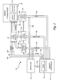
- FIG. 1 is a block diagram according to an embodiment of the present invention.
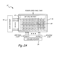
- FIGS. 2A-2C are block diagrams illustrating addressing of data bits in a memory storage device according to embodiments of the present invention.
- FIG. 3 is a flowchart illustrating a method of detecting and handling permanent bit errors in memory storage devices according to an embodiment of the present invention.
- the present invention describes a memory system that automatically detects and handles permanent bit errors, such as single event latchup (SEL) events, without recycling power.
- the system contains a primary memory partition and a secondary memory partition of a memory storage device.
- the primary partition is used for general memory storage and the secondary partition is used upon detection of a permanent bit error.
- a memory controller redirects all future read and write requests for the address associated with the permanent bit error to the secondary memory partition.
- FIG. 1 is a block diagram illustrating an embodiment of memory system 10, which includes memory storage device 12, memory controller 14, error detection and correction (EDAC) controller 16, primary memory storage partition 17, secondary memory storage partition 18, processor 20, EDAC codes module 22, address buses 24a-24d, data buses 26a-26c, address buffer 28, EDAC buffer 30, data buffer 32, control lines 33a-33e, and EDAC buses 34a-34b.
- EDAC controller 16 is an error detector implemented as a part of memory controller 14.
- the term 'error detection and correction' (EDAC) refers broadly to a controller or circuit that is capable of identifying errors in transmitted data and/or correcting detected bit errors.
- an EDAC is capable of detecting single bit errors or multi-bit errors, and may be further capable of correcting single-bit errors and multi-bit errors.
- Algorithms for detecting and correcting multi-bit errors are typically more computationally expensive than algorithms for detecting and/or correcting single-bit errors.
- a standard parity algorithm may be employed to detect single bit errors.
- Memory controller 14 may be implemented using a field programmable gate array (FPGA), or any other suitable programmable logic device.
- Address buffer 28, EDAC buffer 30, and data buffer 32 are implemented due to the bidirectional nature of address buses 24a-24d, data buses 26a-26c, and EDAC buses 34a-34b.
- EDAC codes module 22 is used in conjunction with EDAC controller 16 as part of an EDAC circuit to detect bit errors in memory storage device 12.
- Control lines 33a-33e are used to allow memory controller 14 to communicate with the rest of memory system 10.
- memory storage device 12 contains primary memory storage partition 17 and secondary memory storage partition 18.
- an operating system running on processor 20 issues read and write requests, which are communicated using address bus 24d and data bus 26c. Before reaching memory storage device 12, the read and write requests pass through memory controller 14.
- Memory controller 14 has the ability to redirect read and write requests for primary memory partition 17 to secondary memory partition 18 transparent to the operating system running on processor 20. Therefore, the operating system is not required to keep track of both primary memory storage partition 17 and secondary memory storage partition 18. For example, if memory storage device 12 is 4 kilobytes in size, then primary memory storage partition 17 and secondary memory storage partition 18 would each be 2 kilobytes in size.
- memory storage device 12 is byte addressable then the operating system running on processor 20 would only be required to know of, and use, 11 address bits to access data in primary memory storage partition 17.
- Memory controller 14 would use the 12th address bit to select between primary memory storage partition 17 and secondary memory storage partition 18.
- Memory system 10 can be implemented such that memory controller 14 could use any of the 12 bits as the partition select bit, leaving the operating system to use the remaining 11 bits for addressing, which allows flexibility in how memory storage device 12 is partitioned.
- EDAC controller 16 handles detection of single and multiple bit errors in data words stored in memory storage device 12. When data is returned from memory storage device 12, the EDAC controller checks the data for bit errors before returning the data to processor 20. These bit errors can be caused by a non-permanent event, such as an SEU event, or by a permanent event, such as an SEL event. To differentiate between permanent bit errors and non-permanent bit errors, EDAC controller 16 checks to see if a bit error was detected the previous time this address in memory storage device 12 was accessed. If there was not a previous bit error detected, then EDAC controller 16 assumes a non-permanent bit error (i.e.
- EDAC controller 16 checks to see if there is still a bit error. If there is no longer a bit error detected for this address, then EDAC controller 16 assumes the previous bit error was a non-permanent bit error and has been corrected. If there is still a bit error detected, then the location in memory storage device 12 is assumed to have a permanent bit error (i.e. an SEL event). EDAC controller 16 then provides processor 20 and secondary memory storage partition 18 with the correct data. EDAC controller 16 also flags the location in primary memory storage partition 17 indicating to memory controller 14 that all future requests for this address should be redirected to secondary memory storage partition 18 of memory storage device 12. This redirection by memory controller 14 continues until the system is powered down.
- FIG. 2A is a diagram illustrating an embodiment of memory block 36 contained in memory storage device 12.
- the rows and columns of memory block 36 are composed of data storage bit cells 42.
- Cells 42 may be made up of one or more MOSFET transistors (not shown).
- Column decoder 38 and row decoder 40 are used to access data from the bit cells, for example, from cell 44.
- FIG. 2B is a diagram showing an embodiment of an addressing scheme for memory block 36 of memory storage device 12.
- data words have a length of seven bits.
- Cells 42 are arranged such that each bit of a data word is separated by the length of the data word. Having the data bits addressed in this way is advantageous because single bit errors in data words are easier to handle than multiple bit errors.
- Energized particles can hit a cell 42 and cause a cascading effect, flipping bits in multiple adjacent cells which, in systems not addressed according to the current embodiment, increases the chances of having multiple bit errors in data words.
- cell 46a corresponds to address 0
- bit 0, cell 46b corresponds to address 1
- bit 0, cell 46c corresponds to address 2
- bit 0, cell 48a corresponds to address 0, bit 1
- cell 48b corresponds to address 1, bit 1, physically separating the data bits corresponding to the same address by the length of the data word, which protects against multiple bit errors.
- FIG. 2C is a diagram illustrating multiple memory blocks 36 in a memory storage device 12.
- Memory storage device 12 may be implemented such that data bit storage cells 42 are adjacent not only in the horizontal direction, but in the vertical direction as well.
- bit cells may be arranged such that adjacent cells 50a-50d are separated in the vertical direction by a fixed address differential.
- Vertically adjacent cells 50a-50d can be affected in the same way that horizontally adjacent cells 46a-46c are affected by an energized particle.
- memory storage device 12 should be partitioned such that corresponding addresses in primary memory storage partition 17 and secondary memory storage partition 18 are not vertically adjacent. This will help protect against an energized particle creating bit errors occurring for the same data word in primary memory storage partition 17 and secondary memory storage partition 18.
- FIG. 3 is a flowchart illustrating a detailed method 62 of detecting and handling permanent bit errors in memory storage devices according to an embodiment of the present invention.
- processor 20 issues a read or a write request on address bus 24d and data bus 26c.
- EDAC controller 16 determines whether there has been a previous permanent bit error detected at the address associated with the read or write request.
- the read or write request is redirected by memory controller 14 to secondary memory storage partition 18 of memory storage device 12 and the data is returned to the processor 20.
- EDAC controller 16 checks the data stored in primary memory storage partition 17 of data storage device 12 for single or multiple bit errors. At step 72, if there are no bit errors detected, then the correct data is simply returned to processor 20. At step 74, if there is a bit error detected then EDAC controller 16 determines if this is the second consecutive bit error detected for this location in primary memory storage partition 17 of memory storage device 12. At step 78, if this is not the second error at this location, then EDAC controller 16 corrects the data in memory storage device 12, returns the corrected data to processor 20, and logs the address associated with the bit error.
- EDAC controller 16 logs this address as having a permanent bit error, returns the corrected data to processor 20, and memory controller 14 redirects all future read and write requests for this location to a corresponding location in secondary memory storage partition 18 of memory storage device 12.
- memory storage device 12 may be implemented using a static random access memory device, a dynamic random access memory device, or any other device susceptible to permanent bit errors.
Landscapes
- Engineering & Computer Science (AREA)
- Theoretical Computer Science (AREA)
- Quality & Reliability (AREA)
- Physics & Mathematics (AREA)
- General Engineering & Computer Science (AREA)
- General Physics & Mathematics (AREA)
- Techniques For Improving Reliability Of Storages (AREA)
Abstract
Description
- The present invention is related to error correction in memory systems, and in particular to a system and method for automatically detecting and handling permanent bit errors in memory systems.
- Computer systems generally contain, at minimum, a central processing unit and a memory storage device. Memory storage devices are necessary because they provide data retention for the computer system. These memory storage devices are susceptible to data bit errors, especially in environments with high levels of radiation. These bit errors occur when an energized particle, such as a stray neutron, comes into contact with a data bit storage cell and causes the stored data bit to flip from a
logic 1 to alogic 0 or vice versa. - Computer systems are usually equipped to detect single or multiple bit errors in the data stored in a memory storage device. These errors can be temporary, such as bit errors caused by a single event upset (SEU), or permanent, such as bit errors caused by single event latchup (SEL) events, which require a reset of power to the memory storage device to fix. An SEU event is caused when an energized particle comes into contact with a data bit storage cell causing the storage cell to change state. An SEU event can be fixed by simply rewriting the correct data to the data bit storage cell. In contrast, an SEL event generally occurs when an energized particle, usually a stray neutron, hits a metal oxide semiconductor field effect transistor (MOSFET) and creates a low-impedance path between the power rails of the transistor causing it to continuously conduct. The transistor remains in this state as long as there is some current flowing through it, which is generally until the power is cycled.
- The prior art involves handling permanent bit errors by detecting the error and then automatically recycling power to the device. In flight applications, for example, powering down the latched device requires special circuitry to be added to the power supply to interrupt the input power and to allow the energy in the system to deplete before reapplying the input power. During this period of time, the system must remain offline.
- Recycling power to the memory storage device can cause problems in systems that cannot be offline for any extended period of time, such as the systems for an aircraft. Thus, systems that are susceptible to permanent bit errors, particularly in environments that are exposed to high radiation, are required to use memory storage devices that are insulated as to be incapable of permanent bit errors. These memory storage devices are often more expensive than those that are susceptible to permanent bit errors.
- The present invention relates to a memory system including a primary memory storage partition, a secondary memory storage partition, and a memory controller that is connected to read and write to the primary memory storage partition and detect a permanent bit error at an address associated with the primary memory storage partition. In response to a detected permanent bit error, the memory controller stores data from the address associated with the permanent bit error to an address associated with the secondary memory storage partition.
- Viewed from a first aspect, the present invention provides a permanent bit error detection and handling circuit comprising: a primary memory storage partition; a secondary memory storage partition; an error detector for detecting bit errors in data in the primary memory storage partition; and a controller for distinguishing between non-permanent bit errors and permanent bit errors, storing data from an address associated with a detected permanent bit error to the secondary memory storage partition and redirecting subsequent data requests for the address associated with the detected permanent bit error to the secondary memory storage partition.
- Viewed from a second aspect, the present invention provides a memory system comprising: a memory storage device having a primary memory storage partition and a secondary memory storage partition; and a memory controller connected to read and write data to the memory storage device, the memory controller configured to detect bit errors and distinguish between non-permanent and permanent bit errors; wherein the memory controller, in response to a detected permanent bit error in the primary memory storage partition, stores data from the address associated with the permanent bit error to an address associated with the secondary memory storage partition and redirects all subsequent data requests for the address associated with the primary memory storage partition to the address associated with the secondary memory storage partition.
- Viewed from a third aspect, the present invention provides a method for detecting and handling permanent bit errors in a memory storage device having a primary memory storage partition for storing data and a secondary memory storage partition, the method comprising: detecting a bit error at an address associated with the primary memory storage partition; distinguishing between a non-permanent bit error and a permanent bit error; storing data associated with a detected permanent bit error to the secondary memory storage partition; and directing subsequent read and write operations associated with the address of the detected permanent bit error to the secondary memory storage partition.
-
FIG. 1 is a block diagram according to an embodiment of the present invention. -
FIGS. 2A-2C are block diagrams illustrating addressing of data bits in a memory storage device according to embodiments of the present invention. -
FIG. 3 is a flowchart illustrating a method of detecting and handling permanent bit errors in memory storage devices according to an embodiment of the present invention. - The present invention describes a memory system that automatically detects and handles permanent bit errors, such as single event latchup (SEL) events, without recycling power. In particular, the system contains a primary memory partition and a secondary memory partition of a memory storage device. The primary partition is used for general memory storage and the secondary partition is used upon detection of a permanent bit error. Upon detection of a permanent bit error, a memory controller redirects all future read and write requests for the address associated with the permanent bit error to the secondary memory partition.
-
FIG. 1 is a block diagram illustrating an embodiment ofmemory system 10, which includesmemory storage device 12,memory controller 14, error detection and correction (EDAC)controller 16, primarymemory storage partition 17, secondarymemory storage partition 18,processor 20,EDAC codes module 22,address buses 24a-24d,data buses 26a-26c,address buffer 28, EDACbuffer 30,data buffer 32,control lines 33a-33e, and EDACbuses 34a-34b. EDACcontroller 16 is an error detector implemented as a part ofmemory controller 14. The term 'error detection and correction' (EDAC) refers broadly to a controller or circuit that is capable of identifying errors in transmitted data and/or correcting detected bit errors. For example, in one embodiment an EDAC is capable of detecting single bit errors or multi-bit errors, and may be further capable of correcting single-bit errors and multi-bit errors. Algorithms for detecting and correcting multi-bit errors are typically more computationally expensive than algorithms for detecting and/or correcting single-bit errors. For example, a standard parity algorithm may be employed to detect single bit errors. -
Memory controller 14 may be implemented using a field programmable gate array (FPGA), or any other suitable programmable logic device.Address buffer 28, EDACbuffer 30, anddata buffer 32 are implemented due to the bidirectional nature ofaddress buses 24a-24d,data buses 26a-26c, and EDACbuses 34a-34b. EDACcodes module 22 is used in conjunction with EDACcontroller 16 as part of an EDAC circuit to detect bit errors inmemory storage device 12.Control lines 33a-33e are used to allowmemory controller 14 to communicate with the rest ofmemory system 10. - To handle permanent bit errors,
memory storage device 12 contains primarymemory storage partition 17 and secondarymemory storage partition 18. In one embodiment, an operating system running onprocessor 20 issues read and write requests, which are communicated usingaddress bus 24d anddata bus 26c. Before reachingmemory storage device 12, the read and write requests pass throughmemory controller 14.Memory controller 14 has the ability to redirect read and write requests forprimary memory partition 17 tosecondary memory partition 18 transparent to the operating system running onprocessor 20. Therefore, the operating system is not required to keep track of both primarymemory storage partition 17 and secondarymemory storage partition 18. For example, ifmemory storage device 12 is 4 kilobytes in size, then primarymemory storage partition 17 and secondarymemory storage partition 18 would each be 2 kilobytes in size. Ifmemory storage device 12 is byte addressable then the operating system running onprocessor 20 would only be required to know of, and use, 11 address bits to access data in primarymemory storage partition 17.Memory controller 14 would use the 12th address bit to select between primarymemory storage partition 17 and secondarymemory storage partition 18.Memory system 10 can be implemented such thatmemory controller 14 could use any of the 12 bits as the partition select bit, leaving the operating system to use the remaining 11 bits for addressing, which allows flexibility in howmemory storage device 12 is partitioned. - EDAC
controller 16 handles detection of single and multiple bit errors in data words stored inmemory storage device 12. When data is returned frommemory storage device 12, the EDAC controller checks the data for bit errors before returning the data toprocessor 20. These bit errors can be caused by a non-permanent event, such as an SEU event, or by a permanent event, such as an SEL event. To differentiate between permanent bit errors and non-permanent bit errors,EDAC controller 16 checks to see if a bit error was detected the previous time this address inmemory storage device 12 was accessed. If there was not a previous bit error detected, then EDACcontroller 16 assumes a non-permanent bit error (i.e. an SEU event) has been detected, provides the operating system running onprocessor 20, andmemory storage device 12 with the corrected data, and flags the address of the non-permanent bit error. The next time there is a read or write request to this address in memory, EDACcontroller 16 checks to see if there is still a bit error. If there is no longer a bit error detected for this address, then EDACcontroller 16 assumes the previous bit error was a non-permanent bit error and has been corrected. If there is still a bit error detected, then the location inmemory storage device 12 is assumed to have a permanent bit error (i.e. an SEL event). EDACcontroller 16 then providesprocessor 20 and secondarymemory storage partition 18 with the correct data. EDACcontroller 16 also flags the location in primarymemory storage partition 17 indicating tomemory controller 14 that all future requests for this address should be redirected to secondarymemory storage partition 18 ofmemory storage device 12. This redirection bymemory controller 14 continues until the system is powered down. -
FIG. 2A is a diagram illustrating an embodiment ofmemory block 36 contained inmemory storage device 12. The rows and columns ofmemory block 36 are composed of datastorage bit cells 42.Cells 42 may be made up of one or more MOSFET transistors (not shown).Column decoder 38 androw decoder 40 are used to access data from the bit cells, for example, fromcell 44. -
FIG. 2B is a diagram showing an embodiment of an addressing scheme formemory block 36 ofmemory storage device 12. In this embodiment, data words have a length of seven bits.Cells 42 are arranged such that each bit of a data word is separated by the length of the data word. Having the data bits addressed in this way is advantageous because single bit errors in data words are easier to handle than multiple bit errors. Energized particles can hit acell 42 and cause a cascading effect, flipping bits in multiple adjacent cells which, in systems not addressed according to the current embodiment, increases the chances of having multiple bit errors in data words. For example,cell 46a corresponds to address 0,bit 0,cell 46b corresponds to address 1,bit 0,cell 46c corresponds to address 2,bit 0,cell 48a corresponds to address 0,bit 1, andcell 48b corresponds to address 1,bit 1, physically separating the data bits corresponding to the same address by the length of the data word, which protects against multiple bit errors. -
FIG. 2C is a diagram illustrating multiple memory blocks 36 in amemory storage device 12.Memory storage device 12 may be implemented such that data bitstorage cells 42 are adjacent not only in the horizontal direction, but in the vertical direction as well. In this embodiment, bit cells may be arranged such thatadjacent cells 50a-50d are separated in the vertical direction by a fixed address differential. Verticallyadjacent cells 50a-50d can be affected in the same way that horizontallyadjacent cells 46a-46c are affected by an energized particle. Thus,memory storage device 12 should be partitioned such that corresponding addresses in primarymemory storage partition 17 and secondarymemory storage partition 18 are not vertically adjacent. This will help protect against an energized particle creating bit errors occurring for the same data word in primarymemory storage partition 17 and secondarymemory storage partition 18. -
FIG. 3 is a flowchart illustrating adetailed method 62 of detecting and handling permanent bit errors in memory storage devices according to an embodiment of the present invention. Atstep 64,processor 20 issues a read or a write request onaddress bus 24d anddata bus 26c. Atstep 66,EDAC controller 16 determines whether there has been a previous permanent bit error detected at the address associated with the read or write request. Atstep 68, if there has been a previous permanent bit error detected, then the read or write request is redirected bymemory controller 14 to secondarymemory storage partition 18 ofmemory storage device 12 and the data is returned to theprocessor 20. Atstep 70, if there has not been a previous permanent bit error detected at this address, thenEDAC controller 16 checks the data stored in primarymemory storage partition 17 ofdata storage device 12 for single or multiple bit errors. Atstep 72, if there are no bit errors detected, then the correct data is simply returned toprocessor 20. Atstep 74, if there is a bit error detected thenEDAC controller 16 determines if this is the second consecutive bit error detected for this location in primarymemory storage partition 17 ofmemory storage device 12. Atstep 78, if this is not the second error at this location, thenEDAC controller 16 corrects the data inmemory storage device 12, returns the corrected data toprocessor 20, and logs the address associated with the bit error. Atstep 76, if this is the second consecutive error at this location,EDAC controller 16 logs this address as having a permanent bit error, returns the corrected data toprocessor 20, andmemory controller 14 redirects all future read and write requests for this location to a corresponding location in secondarymemory storage partition 18 ofmemory storage device 12. - In this way, the present invention provides a system and method for detecting and handling permanent bit errors in memory storage devices that does not require a recycling of power to the memory storage device. Although the present invention has been described with reference to preferred embodiments, workers skilled in the art will recognize that changes may be made in form and detail without departing from the scope of the invention, which is defined by the claims. For instance, in
FIG. 1 ,memory storage device 12 may be implemented using a static random access memory device, a dynamic random access memory device, or any other device susceptible to permanent bit errors.
Claims (15)
- A permanent bit error detection and handling circuit comprising:a primary memory storage partition (17);a secondary memory storage partition (18);an error detector for detecting bit errors in data in the primary memory storage partition; anda controller for distinguishing between non-permanent bit errors and permanent bit errors, storing data from an address associated with a detected permanent bit error to the secondary memory storage partition and redirecting subsequent data requests for the address associated with the detected permanent bit error to the secondary memory storage partition.
- The circuit of claim 1, wherein the error detector includes an error detection and correction (EDAC) circuit that detects and corrects bit errors in the primary and secondary memory storage partitions.
- The circuit of claim 2, wherein in response to a detected bit error by the error detector, the controller stores an address associated with the detected bit error.
- The circuit of claim 3, wherein the controller identifies a bit error detected by the error detector as a permanent error, if the address associated with the detected bit error was previously stored by the controller as associated with a detected bit error.
- The circuit of claim 4, wherein the controller removes a stored address associated with a detected bit error if no errors are detected in a subsequent read/write operation associated with the address.
- The circuit of any preceding claim, wherein the primary memory storage partition and the secondary memory storage partition are implemented as logical partitions on a single memory storage device (12).
- The circuit of claim 6, wherein corresponding addresses in the primary memory storage partition and the secondary memory storage partition are not vertically adjacent to one another in the single memory storage device.
- The circuit of claim 6 or 7, wherein the single memory storage device comprises a static random access memory device.
- The circuit of any preceding claim, wherein the secondary memory storage partition is invisible to a processor (20) issuing read and write requests to the primary memory storage partition.
- A memory system (10) comprising:the circuit of any preceding claim,wherein a memory storage device comprises the primary memory storage partition and the secondary memory storage partition; andwherein a memory controller connected to read and write data to the memory storage device comprises the error detector and the controller.
- A method for detecting and handling permanent bit errors in a memory storage device (12) having a primary memory storage partition (17) for storing data and a secondary memory storage (18) partition, the method comprising:detecting a bit error at an address associated with the primary memory storage partition;distinguishing between a non-permanent bit error and a permanent bit error;storing data associated with a detected permanent bit error to the secondary memory storage partition; anddirecting subsequent read and write operations associated with the address of the detected permanent bit error to the secondary memory storage partition.
- The method of claim 11, wherein distinguishing between a non-permanent bit error and a permanent bit error includes:detecting a bit error at an address associated with the primary memory storage partition;correcting data at the address associated with the detected bit error;storing the address associated with the bit error detected in the primary memory storage partition; anddetecting a permanent bit error at the address associated with the primary memory storage partition if a successive bit error is detected at the stored address.
- The method of claim 11 or 12, wherein the primary memory storage partition and the secondary memory storage partition are implemented as logical partitions on a single memory storage device (12).
- The method of claim 13, wherein the single memory storage device comprises a static random access memory device.
- The method of any of claims 11 to 14, wherein directing subsequent read and write operations is invisible to a processor (20) issuing data requests to the primary memory storage partition.
Applications Claiming Priority (1)
| Application Number | Priority Date | Filing Date | Title |
|---|---|---|---|
| US12/871,070 US8397134B2 (en) | 2010-08-30 | 2010-08-30 | System for handling of permanent bit errors in memory devices |
Publications (2)
| Publication Number | Publication Date |
|---|---|
| EP2423815A1 true EP2423815A1 (en) | 2012-02-29 |
| EP2423815B1 EP2423815B1 (en) | 2019-05-15 |
Family
ID=44674363
Family Applications (1)
| Application Number | Title | Priority Date | Filing Date |
|---|---|---|---|
| EP11179431.9A Active EP2423815B1 (en) | 2010-08-30 | 2011-08-30 | System for handling of permanent bit errors in memory devices |
Country Status (2)
| Country | Link |
|---|---|
| US (1) | US8397134B2 (en) |
| EP (1) | EP2423815B1 (en) |
Cited By (2)
| Publication number | Priority date | Publication date | Assignee | Title |
|---|---|---|---|---|
| FR3100347A1 (en) * | 2019-09-04 | 2021-03-05 | Stmicroelectronics (Rousset) Sas | Error detection |
| US11640844B2 (en) | 2019-09-04 | 2023-05-02 | Stmicroelectronics (Rousset) Sas | Error detection |
Families Citing this family (6)
| Publication number | Priority date | Publication date | Assignee | Title |
|---|---|---|---|---|
| US8896978B2 (en) * | 2012-06-15 | 2014-11-25 | Texas Instruments Incorporated | Integrated circuit with automatic deactivation upon exceeding a specific ion linear energy transfer (LET) value |
| US20140310536A1 (en) * | 2013-04-16 | 2014-10-16 | Qualcomm Incorporated | Storage device assisted inline encryption and decryption |
| JP2014215717A (en) * | 2013-04-23 | 2014-11-17 | 富士通株式会社 | Electronic circuit |
| US9384081B2 (en) * | 2014-07-01 | 2016-07-05 | Gogo Llc | Delayed disk recovery |
| WO2016133518A1 (en) * | 2015-02-19 | 2016-08-25 | Hewlett Packard Enterprise Development Lp | Enabling advanced error correction control on subset of memory controllers |
| US11335430B2 (en) | 2019-03-26 | 2022-05-17 | Rambus Inc. | Error remapping |
Citations (6)
| Publication number | Priority date | Publication date | Assignee | Title |
|---|---|---|---|---|
| US4209846A (en) * | 1977-12-02 | 1980-06-24 | Sperry Corporation | Memory error logger which sorts transient errors from solid errors |
| US5925138A (en) * | 1997-03-04 | 1999-07-20 | Micron Electronics, Inc. | Method for allowing data transfers with a memory having defective storage locations |
| US20030217222A1 (en) * | 2002-05-16 | 2003-11-20 | Deutscher Dale W. | Calibration method implementing segmented flash memeory and RAM overlay |
| EP1811525A2 (en) * | 2006-01-18 | 2007-07-25 | Apple Computer, Inc. | Disabling faulty flash memory dies |
| WO2008061558A1 (en) * | 2006-11-21 | 2008-05-29 | Freescale Semiconductor, Inc. | Memory system with ecc-unit and further processing arrangement |
| US20080301529A1 (en) * | 2007-06-01 | 2008-12-04 | Carol Spanel | Apparatus and method for distinguishing single bit errors in memory modules |
Family Cites Families (1)
| Publication number | Priority date | Publication date | Assignee | Title |
|---|---|---|---|---|
| US20050283566A1 (en) * | 2003-09-29 | 2005-12-22 | Rockwell Automation Technologies, Inc. | Self testing and securing ram system and method |
-
2010
- 2010-08-30 US US12/871,070 patent/US8397134B2/en active Active
-
2011
- 2011-08-30 EP EP11179431.9A patent/EP2423815B1/en active Active
Patent Citations (6)
| Publication number | Priority date | Publication date | Assignee | Title |
|---|---|---|---|---|
| US4209846A (en) * | 1977-12-02 | 1980-06-24 | Sperry Corporation | Memory error logger which sorts transient errors from solid errors |
| US5925138A (en) * | 1997-03-04 | 1999-07-20 | Micron Electronics, Inc. | Method for allowing data transfers with a memory having defective storage locations |
| US20030217222A1 (en) * | 2002-05-16 | 2003-11-20 | Deutscher Dale W. | Calibration method implementing segmented flash memeory and RAM overlay |
| EP1811525A2 (en) * | 2006-01-18 | 2007-07-25 | Apple Computer, Inc. | Disabling faulty flash memory dies |
| WO2008061558A1 (en) * | 2006-11-21 | 2008-05-29 | Freescale Semiconductor, Inc. | Memory system with ecc-unit and further processing arrangement |
| US20080301529A1 (en) * | 2007-06-01 | 2008-12-04 | Carol Spanel | Apparatus and method for distinguishing single bit errors in memory modules |
Cited By (6)
| Publication number | Priority date | Publication date | Assignee | Title |
|---|---|---|---|---|
| FR3100347A1 (en) * | 2019-09-04 | 2021-03-05 | Stmicroelectronics (Rousset) Sas | Error detection |
| EP3789879A1 (en) * | 2019-09-04 | 2021-03-10 | STMicroelectronics (Rousset) SAS | Error detection |
| US11115061B2 (en) | 2019-09-04 | 2021-09-07 | Stmicroelectronics (Rousset) Sas | Error detection |
| US11509332B2 (en) | 2019-09-04 | 2022-11-22 | Stmicroelectronics (Rousset) Sas | Error detection |
| US11640844B2 (en) | 2019-09-04 | 2023-05-02 | Stmicroelectronics (Rousset) Sas | Error detection |
| US11742050B2 (en) | 2019-09-04 | 2023-08-29 | Stmicroelectronics (Rousset) Sas | Error detection |
Also Published As
| Publication number | Publication date |
|---|---|
| US8397134B2 (en) | 2013-03-12 |
| US20120054570A1 (en) | 2012-03-01 |
| EP2423815B1 (en) | 2019-05-15 |
Similar Documents
| Publication | Publication Date | Title |
|---|---|---|
| EP2423815B1 (en) | System for handling of permanent bit errors in memory devices | |
| US10019312B2 (en) | Error monitoring of a memory device containing embedded error correction | |
| US9940457B2 (en) | Detecting a cryogenic attack on a memory device with embedded error correction | |
| CN105843699B (en) | Dynamic random access memory device and method for error monitoring and correction | |
| US6700827B2 (en) | Cam circuit with error correction | |
| US11568917B1 (en) | Hammer refresh row address detector, and semiconductor memory device and memory module including the same | |
| US11204825B2 (en) | Memory device and repair method with column-based error code tracking | |
| US9529667B2 (en) | DRAM error correction event notification | |
| US9146808B1 (en) | Soft error protection for content addressable memory | |
| US9208024B2 (en) | Memory ECC with hard and soft error detection and management | |
| US20120266041A1 (en) | Systems and methods for error detection and correction in a memory module which includes a memory buffer | |
| US9645904B2 (en) | Dynamic cache row fail accumulation due to catastrophic failure | |
| US11782807B2 (en) | Memory module with dedicated repair devices | |
| US20180165152A1 (en) | Adaptive error correction in memory devices | |
| US10839935B2 (en) | Dynamic redundancy for memory | |
| US20190056874A1 (en) | System and method for preserving data in volatile memory | |
| US9823962B2 (en) | Soft error detection in a memory system | |
| US10481973B2 (en) | Memory module with dedicated repair devices | |
| US20180052615A1 (en) | Soft error detection in a memory system | |
| US7523364B2 (en) | Double DRAM bit steering for multiple error corrections | |
| JP2005004947A (en) | Memory device and memory error correction method | |
| US10108486B2 (en) | Error protection | |
| US9727408B2 (en) | Memory error detection system | |
| JPH02143352A (en) | Memory error detection and correction system | |
| JPS61261896A (en) | Semiconductor memory device |
Legal Events
| Date | Code | Title | Description |
|---|---|---|---|
| AK | Designated contracting states |
Kind code of ref document: A1 Designated state(s): AL AT BE BG CH CY CZ DE DK EE ES FI FR GB GR HR HU IE IS IT LI LT LU LV MC MK MT NL NO PL PT RO RS SE SI SK SM TR |
|
| AX | Request for extension of the european patent |
Extension state: BA ME |
|
| PUAI | Public reference made under article 153(3) epc to a published international application that has entered the european phase |
Free format text: ORIGINAL CODE: 0009012 |
|
| 17P | Request for examination filed |
Effective date: 20120829 |
|
| STAA | Information on the status of an ep patent application or granted ep patent |
Free format text: STATUS: EXAMINATION IS IN PROGRESS |
|
| 17Q | First examination report despatched |
Effective date: 20170315 |
|
| GRAP | Despatch of communication of intention to grant a patent |
Free format text: ORIGINAL CODE: EPIDOSNIGR1 |
|
| STAA | Information on the status of an ep patent application or granted ep patent |
Free format text: STATUS: GRANT OF PATENT IS INTENDED |
|
| GRAJ | Information related to disapproval of communication of intention to grant by the applicant or resumption of examination proceedings by the epo deleted |
Free format text: ORIGINAL CODE: EPIDOSDIGR1 |
|
| STAA | Information on the status of an ep patent application or granted ep patent |
Free format text: STATUS: EXAMINATION IS IN PROGRESS |
|
| INTG | Intention to grant announced |
Effective date: 20180927 |
|
| GRAP | Despatch of communication of intention to grant a patent |
Free format text: ORIGINAL CODE: EPIDOSNIGR1 |
|
| STAA | Information on the status of an ep patent application or granted ep patent |
Free format text: STATUS: GRANT OF PATENT IS INTENDED |
|
| INTC | Intention to grant announced (deleted) | ||
| INTG | Intention to grant announced |
Effective date: 20181127 |
|
| GRAS | Grant fee paid |
Free format text: ORIGINAL CODE: EPIDOSNIGR3 |
|
| GRAA | (expected) grant |
Free format text: ORIGINAL CODE: 0009210 |
|
| STAA | Information on the status of an ep patent application or granted ep patent |
Free format text: STATUS: THE PATENT HAS BEEN GRANTED |
|
| AK | Designated contracting states |
Kind code of ref document: B1 Designated state(s): AL AT BE BG CH CY CZ DE DK EE ES FI FR GB GR HR HU IE IS IT LI LT LU LV MC MK MT NL NO PL PT RO RS SE SI SK SM TR |
|
| REG | Reference to a national code |
Ref country code: CH Ref legal event code: EP Ref country code: GB Ref legal event code: FG4D |
|
| REG | Reference to a national code |
Ref country code: DE Ref legal event code: R096 Ref document number: 602011058945 Country of ref document: DE |
|
| REG | Reference to a national code |
Ref country code: IE Ref legal event code: FG4D |
|
| REG | Reference to a national code |
Ref country code: NL Ref legal event code: MP Effective date: 20190515 |
|
| REG | Reference to a national code |
Ref country code: LT Ref legal event code: MG4D |
|
| PG25 | Lapsed in a contracting state [announced via postgrant information from national office to epo] |
Ref country code: NL Free format text: LAPSE BECAUSE OF FAILURE TO SUBMIT A TRANSLATION OF THE DESCRIPTION OR TO PAY THE FEE WITHIN THE PRESCRIBED TIME-LIMIT Effective date: 20190515 Ref country code: SE Free format text: LAPSE BECAUSE OF FAILURE TO SUBMIT A TRANSLATION OF THE DESCRIPTION OR TO PAY THE FEE WITHIN THE PRESCRIBED TIME-LIMIT Effective date: 20190515 Ref country code: LT Free format text: LAPSE BECAUSE OF FAILURE TO SUBMIT A TRANSLATION OF THE DESCRIPTION OR TO PAY THE FEE WITHIN THE PRESCRIBED TIME-LIMIT Effective date: 20190515 Ref country code: FI Free format text: LAPSE BECAUSE OF FAILURE TO SUBMIT A TRANSLATION OF THE DESCRIPTION OR TO PAY THE FEE WITHIN THE PRESCRIBED TIME-LIMIT Effective date: 20190515 Ref country code: AL Free format text: LAPSE BECAUSE OF FAILURE TO SUBMIT A TRANSLATION OF THE DESCRIPTION OR TO PAY THE FEE WITHIN THE PRESCRIBED TIME-LIMIT Effective date: 20190515 Ref country code: ES Free format text: LAPSE BECAUSE OF FAILURE TO SUBMIT A TRANSLATION OF THE DESCRIPTION OR TO PAY THE FEE WITHIN THE PRESCRIBED TIME-LIMIT Effective date: 20190515 Ref country code: PT Free format text: LAPSE BECAUSE OF FAILURE TO SUBMIT A TRANSLATION OF THE DESCRIPTION OR TO PAY THE FEE WITHIN THE PRESCRIBED TIME-LIMIT Effective date: 20190915 Ref country code: NO Free format text: LAPSE BECAUSE OF FAILURE TO SUBMIT A TRANSLATION OF THE DESCRIPTION OR TO PAY THE FEE WITHIN THE PRESCRIBED TIME-LIMIT Effective date: 20190815 Ref country code: HR Free format text: LAPSE BECAUSE OF FAILURE TO SUBMIT A TRANSLATION OF THE DESCRIPTION OR TO PAY THE FEE WITHIN THE PRESCRIBED TIME-LIMIT Effective date: 20190515 |
|
| PG25 | Lapsed in a contracting state [announced via postgrant information from national office to epo] |
Ref country code: GR Free format text: LAPSE BECAUSE OF FAILURE TO SUBMIT A TRANSLATION OF THE DESCRIPTION OR TO PAY THE FEE WITHIN THE PRESCRIBED TIME-LIMIT Effective date: 20190816 Ref country code: BG Free format text: LAPSE BECAUSE OF FAILURE TO SUBMIT A TRANSLATION OF THE DESCRIPTION OR TO PAY THE FEE WITHIN THE PRESCRIBED TIME-LIMIT Effective date: 20190815 Ref country code: LV Free format text: LAPSE BECAUSE OF FAILURE TO SUBMIT A TRANSLATION OF THE DESCRIPTION OR TO PAY THE FEE WITHIN THE PRESCRIBED TIME-LIMIT Effective date: 20190515 Ref country code: RS Free format text: LAPSE BECAUSE OF FAILURE TO SUBMIT A TRANSLATION OF THE DESCRIPTION OR TO PAY THE FEE WITHIN THE PRESCRIBED TIME-LIMIT Effective date: 20190515 |
|
| REG | Reference to a national code |
Ref country code: AT Ref legal event code: MK05 Ref document number: 1134250 Country of ref document: AT Kind code of ref document: T Effective date: 20190515 |
|
| PG25 | Lapsed in a contracting state [announced via postgrant information from national office to epo] |
Ref country code: EE Free format text: LAPSE BECAUSE OF FAILURE TO SUBMIT A TRANSLATION OF THE DESCRIPTION OR TO PAY THE FEE WITHIN THE PRESCRIBED TIME-LIMIT Effective date: 20190515 Ref country code: AT Free format text: LAPSE BECAUSE OF FAILURE TO SUBMIT A TRANSLATION OF THE DESCRIPTION OR TO PAY THE FEE WITHIN THE PRESCRIBED TIME-LIMIT Effective date: 20190515 Ref country code: DK Free format text: LAPSE BECAUSE OF FAILURE TO SUBMIT A TRANSLATION OF THE DESCRIPTION OR TO PAY THE FEE WITHIN THE PRESCRIBED TIME-LIMIT Effective date: 20190515 Ref country code: RO Free format text: LAPSE BECAUSE OF FAILURE TO SUBMIT A TRANSLATION OF THE DESCRIPTION OR TO PAY THE FEE WITHIN THE PRESCRIBED TIME-LIMIT Effective date: 20190515 Ref country code: CZ Free format text: LAPSE BECAUSE OF FAILURE TO SUBMIT A TRANSLATION OF THE DESCRIPTION OR TO PAY THE FEE WITHIN THE PRESCRIBED TIME-LIMIT Effective date: 20190515 Ref country code: SK Free format text: LAPSE BECAUSE OF FAILURE TO SUBMIT A TRANSLATION OF THE DESCRIPTION OR TO PAY THE FEE WITHIN THE PRESCRIBED TIME-LIMIT Effective date: 20190515 |
|
| REG | Reference to a national code |
Ref country code: DE Ref legal event code: R097 Ref document number: 602011058945 Country of ref document: DE |
|
| PG25 | Lapsed in a contracting state [announced via postgrant information from national office to epo] |
Ref country code: SM Free format text: LAPSE BECAUSE OF FAILURE TO SUBMIT A TRANSLATION OF THE DESCRIPTION OR TO PAY THE FEE WITHIN THE PRESCRIBED TIME-LIMIT Effective date: 20190515 Ref country code: IT Free format text: LAPSE BECAUSE OF FAILURE TO SUBMIT A TRANSLATION OF THE DESCRIPTION OR TO PAY THE FEE WITHIN THE PRESCRIBED TIME-LIMIT Effective date: 20190515 |
|
| PLBE | No opposition filed within time limit |
Free format text: ORIGINAL CODE: 0009261 |
|
| STAA | Information on the status of an ep patent application or granted ep patent |
Free format text: STATUS: NO OPPOSITION FILED WITHIN TIME LIMIT |
|
| PG25 | Lapsed in a contracting state [announced via postgrant information from national office to epo] |
Ref country code: TR Free format text: LAPSE BECAUSE OF FAILURE TO SUBMIT A TRANSLATION OF THE DESCRIPTION OR TO PAY THE FEE WITHIN THE PRESCRIBED TIME-LIMIT Effective date: 20190515 |
|
| 26N | No opposition filed |
Effective date: 20200218 |
|
| PG25 | Lapsed in a contracting state [announced via postgrant information from national office to epo] |
Ref country code: PL Free format text: LAPSE BECAUSE OF FAILURE TO SUBMIT A TRANSLATION OF THE DESCRIPTION OR TO PAY THE FEE WITHIN THE PRESCRIBED TIME-LIMIT Effective date: 20190515 |
|
| PG25 | Lapsed in a contracting state [announced via postgrant information from national office to epo] |
Ref country code: MC Free format text: LAPSE BECAUSE OF FAILURE TO SUBMIT A TRANSLATION OF THE DESCRIPTION OR TO PAY THE FEE WITHIN THE PRESCRIBED TIME-LIMIT Effective date: 20190515 Ref country code: LU Free format text: LAPSE BECAUSE OF NON-PAYMENT OF DUE FEES Effective date: 20190830 Ref country code: SI Free format text: LAPSE BECAUSE OF FAILURE TO SUBMIT A TRANSLATION OF THE DESCRIPTION OR TO PAY THE FEE WITHIN THE PRESCRIBED TIME-LIMIT Effective date: 20190515 Ref country code: CH Free format text: LAPSE BECAUSE OF NON-PAYMENT OF DUE FEES Effective date: 20190831 Ref country code: LI Free format text: LAPSE BECAUSE OF NON-PAYMENT OF DUE FEES Effective date: 20190831 |
|
| REG | Reference to a national code |
Ref country code: BE Ref legal event code: MM Effective date: 20190831 |
|
| PG25 | Lapsed in a contracting state [announced via postgrant information from national office to epo] |
Ref country code: IE Free format text: LAPSE BECAUSE OF NON-PAYMENT OF DUE FEES Effective date: 20190830 |
|
| PG25 | Lapsed in a contracting state [announced via postgrant information from national office to epo] |
Ref country code: BE Free format text: LAPSE BECAUSE OF NON-PAYMENT OF DUE FEES Effective date: 20190831 |
|
| PG25 | Lapsed in a contracting state [announced via postgrant information from national office to epo] |
Ref country code: CY Free format text: LAPSE BECAUSE OF FAILURE TO SUBMIT A TRANSLATION OF THE DESCRIPTION OR TO PAY THE FEE WITHIN THE PRESCRIBED TIME-LIMIT Effective date: 20190515 |
|
| PG25 | Lapsed in a contracting state [announced via postgrant information from national office to epo] |
Ref country code: IS Free format text: LAPSE BECAUSE OF FAILURE TO SUBMIT A TRANSLATION OF THE DESCRIPTION OR TO PAY THE FEE WITHIN THE PRESCRIBED TIME-LIMIT Effective date: 20190915 |
|
| PG25 | Lapsed in a contracting state [announced via postgrant information from national office to epo] |
Ref country code: MT Free format text: LAPSE BECAUSE OF FAILURE TO SUBMIT A TRANSLATION OF THE DESCRIPTION OR TO PAY THE FEE WITHIN THE PRESCRIBED TIME-LIMIT Effective date: 20190515 Ref country code: HU Free format text: LAPSE BECAUSE OF FAILURE TO SUBMIT A TRANSLATION OF THE DESCRIPTION OR TO PAY THE FEE WITHIN THE PRESCRIBED TIME-LIMIT; INVALID AB INITIO Effective date: 20110830 |
|
| PG25 | Lapsed in a contracting state [announced via postgrant information from national office to epo] |
Ref country code: MK Free format text: LAPSE BECAUSE OF FAILURE TO SUBMIT A TRANSLATION OF THE DESCRIPTION OR TO PAY THE FEE WITHIN THE PRESCRIBED TIME-LIMIT Effective date: 20190515 |
|
| P01 | Opt-out of the competence of the unified patent court (upc) registered |
Effective date: 20230522 |
|
| PGFP | Annual fee paid to national office [announced via postgrant information from national office to epo] |
Ref country code: DE Payment date: 20250724 Year of fee payment: 15 |
|
| PGFP | Annual fee paid to national office [announced via postgrant information from national office to epo] |
Ref country code: GB Payment date: 20250725 Year of fee payment: 15 |
|
| PGFP | Annual fee paid to national office [announced via postgrant information from national office to epo] |
Ref country code: FR Payment date: 20250723 Year of fee payment: 15 |