EP2421037A1 - Electronic device mounting structure and electronic device mounting method - Google Patents
Electronic device mounting structure and electronic device mounting method Download PDFInfo
- Publication number
- EP2421037A1 EP2421037A1 EP10764239A EP10764239A EP2421037A1 EP 2421037 A1 EP2421037 A1 EP 2421037A1 EP 10764239 A EP10764239 A EP 10764239A EP 10764239 A EP10764239 A EP 10764239A EP 2421037 A1 EP2421037 A1 EP 2421037A1
- Authority
- EP
- European Patent Office
- Prior art keywords
- principal surface
- projecting portion
- electronic device
- supporting substrate
- hole
- Prior art date
- Legal status (The legal status is an assumption and is not a legal conclusion. Google has not performed a legal analysis and makes no representation as to the accuracy of the status listed.)
- Withdrawn
Links
Images










Classifications
-
- H—ELECTRICITY
- H10—SEMICONDUCTOR DEVICES; ELECTRIC SOLID-STATE DEVICES NOT OTHERWISE PROVIDED FOR
- H10W—GENERIC PACKAGES, INTERCONNECTIONS, CONNECTORS OR OTHER CONSTRUCTIONAL DETAILS OF DEVICES COVERED BY CLASS H10
- H10W20/00—Interconnections in chips, wafers or substrates
- H10W20/01—Manufacture or treatment
- H10W20/021—Manufacture or treatment of interconnections within wafers or substrates
- H10W20/023—Manufacture or treatment of interconnections within wafers or substrates the interconnections being through-semiconductor vias
-
- H—ELECTRICITY
- H10—SEMICONDUCTOR DEVICES; ELECTRIC SOLID-STATE DEVICES NOT OTHERWISE PROVIDED FOR
- H10W—GENERIC PACKAGES, INTERCONNECTIONS, CONNECTORS OR OTHER CONSTRUCTIONAL DETAILS OF DEVICES COVERED BY CLASS H10
- H10W20/00—Interconnections in chips, wafers or substrates
- H10W20/01—Manufacture or treatment
- H10W20/021—Manufacture or treatment of interconnections within wafers or substrates
- H10W20/023—Manufacture or treatment of interconnections within wafers or substrates the interconnections being through-semiconductor vias
- H10W20/0245—Manufacture or treatment of interconnections within wafers or substrates the interconnections being through-semiconductor vias comprising use of blind vias during the manufacture
-
- H—ELECTRICITY
- H10—SEMICONDUCTOR DEVICES; ELECTRIC SOLID-STATE DEVICES NOT OTHERWISE PROVIDED FOR
- H10W—GENERIC PACKAGES, INTERCONNECTIONS, CONNECTORS OR OTHER CONSTRUCTIONAL DETAILS OF DEVICES COVERED BY CLASS H10
- H10W20/00—Interconnections in chips, wafers or substrates
- H10W20/01—Manufacture or treatment
- H10W20/021—Manufacture or treatment of interconnections within wafers or substrates
- H10W20/023—Manufacture or treatment of interconnections within wafers or substrates the interconnections being through-semiconductor vias
- H10W20/0249—Manufacture or treatment of interconnections within wafers or substrates the interconnections being through-semiconductor vias wherein the through-semiconductor via protrudes from backsides of the chips, wafers or substrates during the manufacture
-
- H—ELECTRICITY
- H10—SEMICONDUCTOR DEVICES; ELECTRIC SOLID-STATE DEVICES NOT OTHERWISE PROVIDED FOR
- H10W—GENERIC PACKAGES, INTERCONNECTIONS, CONNECTORS OR OTHER CONSTRUCTIONAL DETAILS OF DEVICES COVERED BY CLASS H10
- H10W20/00—Interconnections in chips, wafers or substrates
- H10W20/20—Interconnections within wafers or substrates, e.g. through-silicon vias [TSV]
-
- H—ELECTRICITY
- H10—SEMICONDUCTOR DEVICES; ELECTRIC SOLID-STATE DEVICES NOT OTHERWISE PROVIDED FOR
- H10W—GENERIC PACKAGES, INTERCONNECTIONS, CONNECTORS OR OTHER CONSTRUCTIONAL DETAILS OF DEVICES COVERED BY CLASS H10
- H10W70/00—Package substrates; Interposers; Redistribution layers [RDL]
- H10W70/01—Manufacture or treatment
- H10W70/05—Manufacture or treatment of insulating or insulated package substrates, or of interposers, or of redistribution layers
- H10W70/093—Connecting or disconnecting other interconnections thereto or therefrom, e.g. connecting bond wires or bumps
-
- H—ELECTRICITY
- H10—SEMICONDUCTOR DEVICES; ELECTRIC SOLID-STATE DEVICES NOT OTHERWISE PROVIDED FOR
- H10W—GENERIC PACKAGES, INTERCONNECTIONS, CONNECTORS OR OTHER CONSTRUCTIONAL DETAILS OF DEVICES COVERED BY CLASS H10
- H10W90/00—Package configurations
-
- H—ELECTRICITY
- H10—SEMICONDUCTOR DEVICES; ELECTRIC SOLID-STATE DEVICES NOT OTHERWISE PROVIDED FOR
- H10W—GENERIC PACKAGES, INTERCONNECTIONS, CONNECTORS OR OTHER CONSTRUCTIONAL DETAILS OF DEVICES COVERED BY CLASS H10
- H10W90/00—Package configurations
- H10W90/701—Package configurations characterised by the relative positions of pads or connectors relative to package parts
-
- H—ELECTRICITY
- H10—SEMICONDUCTOR DEVICES; ELECTRIC SOLID-STATE DEVICES NOT OTHERWISE PROVIDED FOR
- H10W—GENERIC PACKAGES, INTERCONNECTIONS, CONNECTORS OR OTHER CONSTRUCTIONAL DETAILS OF DEVICES COVERED BY CLASS H10
- H10W90/00—Package configurations
- H10W90/20—Configurations of stacked chips
- H10W90/26—Configurations of stacked chips the stacked chips being of the same size without any chips being laterally offset, e.g. chip stacks having a rectangular shape
-
- H—ELECTRICITY
- H10—SEMICONDUCTOR DEVICES; ELECTRIC SOLID-STATE DEVICES NOT OTHERWISE PROVIDED FOR
- H10W—GENERIC PACKAGES, INTERCONNECTIONS, CONNECTORS OR OTHER CONSTRUCTIONAL DETAILS OF DEVICES COVERED BY CLASS H10
- H10W90/00—Package configurations
- H10W90/20—Configurations of stacked chips
- H10W90/297—Configurations of stacked chips characterised by the through-semiconductor vias [TSVs] in the stacked chips
-
- H—ELECTRICITY
- H10—SEMICONDUCTOR DEVICES; ELECTRIC SOLID-STATE DEVICES NOT OTHERWISE PROVIDED FOR
- H10W—GENERIC PACKAGES, INTERCONNECTIONS, CONNECTORS OR OTHER CONSTRUCTIONAL DETAILS OF DEVICES COVERED BY CLASS H10
- H10W90/00—Package configurations
- H10W90/701—Package configurations characterised by the relative positions of pads or connectors relative to package parts
- H10W90/721—Package configurations characterised by the relative positions of pads or connectors relative to package parts of bump connectors
- H10W90/722—Package configurations characterised by the relative positions of pads or connectors relative to package parts of bump connectors between stacked chips
-
- H—ELECTRICITY
- H10—SEMICONDUCTOR DEVICES; ELECTRIC SOLID-STATE DEVICES NOT OTHERWISE PROVIDED FOR
- H10W—GENERIC PACKAGES, INTERCONNECTIONS, CONNECTORS OR OTHER CONSTRUCTIONAL DETAILS OF DEVICES COVERED BY CLASS H10
- H10W90/00—Package configurations
- H10W90/701—Package configurations characterised by the relative positions of pads or connectors relative to package parts
- H10W90/721—Package configurations characterised by the relative positions of pads or connectors relative to package parts of bump connectors
- H10W90/724—Package configurations characterised by the relative positions of pads or connectors relative to package parts of bump connectors between a chip and a stacked insulating package substrate, interposer or RDL
Definitions
- the present invention relates to an electronic device mounting structure for mounting an electronic device such as a semiconductor chip on a support member such as an interposer, and to a method of mounting the electronic device.
- an electronic device mounting structure for mounting an electronic device such as a semiconductor chip on a support member such as an interposer, and to a method of mounting the electronic device.
- Patent Document 1 discloses a substrate having a through electrode that is fabricated from a silicon wafer having an embedded insulating layer between a supporting substrate layer and a silicon layer.
- a blind via hole is formed reaching the silicon layer to a depth that allows formation of a recess.
- An inner wall insulating layer is applied onto the blind via hole to form a conductive layer. Then, by removing the silicon layer, the portion of the conductive layer corresponding to the recess is exposed as a wafer outer raised portion.
- Patent Document 2 discloses a method for manufacturing a semiconductor device that includes: laminating three or more semiconductor chips which each have a terminal with two ends projecting from a substrate, on an interposer; positioning the semiconductor chips and the interposer so as to align the adjacent terminals with each other; and bonding the adjacent terminals together in a lot.
- the present invention was achieved in view of the above circumstances, and has an object of providing an electronic device mounting structure and an electronic device mounting method that make it possible to easily mount an electronic device such as a semiconductor chip on a support member such as an interposer.
- an electronic device mounting structure includes: a supporting member that includes a supporting substrate, and a through electrode that penetrates the supporting substrate from a first principal surface that is one principal surface of the supporting substrate to a second principal surface that is the other principal surface, and that includes a projecting portion that projects from the second principal surface; and an electronic device that includes a device substrate on which a circuit is formed, and a through hole that penetrates between both principal surfaces of the device substrate, wherein the electronic device is arranged on the second principal surface of the supporting substrate so that the projecting portion of the supporting member is inserted into the through hole, and the circuit of the electronic device is electrically connected with the projecting portion.
- the electronic device mounting structure includes a plurality of the electronic devices, wherein each of the electronic devices is laminated on the second principal surface of the supporting substrate. It may be arranged such that the supporting member includes, on the second principal surface of the supporting substrate, a plurality of device arrangement regions in which the electronic devices are arranged by the projecting portion. It may be arranged such that the electronic device mounting structure further includes a protective layer that includes the electronic devices within itself. It may be arranged such that a layer of solder is formed on the outer periphery surface of the projecting portion over the entire length of the projecting portion, and the circuit of the electronic device and the projecting portion are electrically connected by solder that is melted out from the layer of solder. It may be arranged such that the supporting member includes a connection terminal on the first principal surface side.
- An electronic device according to a second aspect of the present invention includes the above-described electronic device mounting structure.
- an electronic device mounting method includes: a first step of preparing a supporting member including a supporting substrate, and a through electrode that penetrates the supporting substrate from a first principal surface that is one principal surface of the supporting substrate to a second principal surface that is the other principal surface, and that includes a projecting portion that projects from the second principal surface; a second step of preparing an electronic device that includes a device substrate, and a through hole that penetrates between both principal surfaces of the device substrate; and a third step of arranging the electronic device on the second principal surface of the supporting substrate so that the projecting portion of the supporting member is inserted into the through hole of the electronic device, and electrically connecting the circuit of the electronic device and the projecting portion.
- the first step includes: a step of laminating, on the second principal surface of the supporting substrate, a projecting portion formation auxiliary layer having a thickness greater than the height of the projecting portion; a step of forming a through hole that penetrates from the first principal surface to the second principal surface of the supporting substrate; a step of forming a communication hole extending from the through hole of the supporting substrate to reach the interior of the projecting portion formation auxiliary layer; a step of filling with a conductor the through hole of the supporting substrate and the communication hole; and a step of exposing the second principal surface of the supporting substrate by removing the projecting portion formation auxiliary layer, and forming a through electrode that consists of the conductor, penetrates the supporting substrate from the first principal surface to the second principal surface, and includes the projecting portion that projects from the second principal surface.
- the first step includes: a step of farming a hole in a base material that has a thickness greater than the sum of the thickness of the supporting substrate and the height of the projecting portion from a surface that becomes the first principal surface of the supporting substrate; a step of filling the hole with a conductor; and a step of forming the second principal surface of the supporting substrate by removing a portion of the base material from the opposite side of the first principal surface of the base material until a portion of the conductor is exposed, and forming a through electrode that consists of the conductor, penetrates the supporting substrate from the first principal surface to the second principal surface, and includes the projecting portion that projects from the second principal surface.
- the first step includes a step of forming a layer of solder on the outer periphery surface of the projecting portion over the entire length of the projecting portion
- the third step includes a step of inserting the projecting portion of the supporting member into each through hole of a plurality of the electronic devices to arrange the electronic devices in a layered manner on the second principal surface of the supporting substrate, and a step of electrically connecting all at once each circuit of the plurality of electronic devices and the projecting portion by melting the layer of solder.
- the projecting portion of the support member even after the projecting portion of the support member has been inserted into each through hole of the plurality of electronic devices, it is possible to confirm the position of the projecting portion from above the electronic device. Therefore, high-density mounting of the electronic devices can be easily performed.
- the projecting portion is a unit conductor that is continuous in the lengthwise direction, even if a plurality of electronic devices are mounted in a layered manner, no joining portion will be present between the electronic devices. As a result, it is possible to achieve a lower resistance of the electrical connections among the electronic devices and the reduction of the total thickness of the layered electronic devices.
- FIG. 1A to FIG. 3D show the electronic device mounting structure and mounting method using a supporting member 10, according to a first embodiment of the present invention.
- the supporting member 10 shown in FIGS. 1A and 1B is a supporting member that includes a supporting substrate 11, and a through electrode 13 that penetrates the supporting substrate 11 from a first principal surface 11a that is one principal surface of the supporting substrate 11 to a second principal surface 11b that is the other principal surface, and includes a projecting portion 13a that projects from the second principal surface 11b, in order to mount an electronic devices 6 on the second principal surface 11b side.
- This supporting member 10 may further include a connection terminal 15 such as a solder bump on the first principal surface 11a side, and is capable of electrically connecting the circuit 4 of the electronic device 6, and an external substrate (not shown), such as a printed circuit board, via the through electrode 13, the circuit 14 and the connection terminal 15.
- a connection terminal 15 such as a solder bump on the first principal surface 11a side, and is capable of electrically connecting the circuit 4 of the electronic device 6, and an external substrate (not shown), such as a printed circuit board, via the through electrode 13, the circuit 14 and the connection terminal 15.
- the supporting substrate 11 consists of a semiconductor substrate, such as a silicon (Si) substrate.
- Insulating layers 111, 112 such as a silicon dioxide film (SiO 2 are formed on both principal surfaces 11a and 11b and on the inner wall of a through hole 12, and thereby provide insulation between the circuit 14 and the semiconductor substrate and between the through electrode 13 and the semiconductor substrate.
- the insulating layer 111 is formed as a continuous layer from the first principal surface 11a of the supporting substrate 11 to the inner wall of the through hole 12, but separate insulating layers may be formed on the first principal surface 11a of the supporting substrate 11 and the inner wall of the through hole 12.
- the electronic device 6 that is used in the present embodiment is a semiconductor chip that has a device substrate 1, and a through hole 2 that penetrates both principal surfaces 1a, 1b of the device substrate 1.
- the device substrate 1 is a semiconductor substrate such as a silicon (Si) substrate, and it is preferable to provide an insulating layer 3 on the inner wall of the through hole 2 in order to provide insulation between the projecting portion 13a of the through electrode 13 and the semiconductor substrate.
- the circuit 4 that constitutes the electronic device is formed on the principal surface 1b of the device substrate 1. It is possible to constitute a portion of the circuit 4 as a semiconductor circuit.
- the type of electronic device is not particularly limited, and examples include a memory device or sensor device.
- a pad 5 that is connected to the circuit 4 is formed at the periphery of the through hole 2.
- the pad 5 and the projecting portion 13a are electrically connected by an electrically conductive bonding material 7 such as solder or conductive paste.
- the electronic device 6 is arranged on the second principal surface 11b of the supporting substrate 11 so that the projecting portion 13a of the supporting member 10 is inserted into the through hole 2 of the electronic device 6.
- the circuit 4 of the electronic device 6 and the projecting portion 13a are electrically connected.
- circuit components such as resistors, capacitors, and inductors may be provided on the circuit 14 of the supporting member 10.
- electronic circuit components such as resistors, capacitors, and inductors may be provided on the circuit 14 of the supporting member 10.
- a semiconductor circuit may be formed on the supporting substrate 11.
- the electronic device mounting structure of the present embodiment even after the projecting portion 13a has been inserted into each through hole of the plurality of electronic devices 6, it is possible to confirm the position of the projecting portion 13a from above the electronic devices 6. Therefore, high-density mounting of the electronic devices 6 can be easily performed. Also, since the projecting portion 13a is a unit conductor that is continuous in the lengthwise direction, even if a plurality of electronic devices 6 are mounted in a layered manner, no joining portion will be present between the electronic devices 6. As a result, it is possible to achieve lower resistance of the electrical connections among the electronic devices 6 and reduction of the total thickness of the layered electronic devices 6.
- a projecting portion formation auxiliary layer 16 is laminated on the second principal surface 11b side of the supporting substrate 11, and the through hole 12 is formed that penetrates from the first principal surface 11a of the supporting substrate 11 to the second principal surface 11b.
- the thickness of the projecting portion formation auxiliary layer 16 is greater than the height of the projecting portion 13a that is provided on the supporting member 10.
- the supporting substrate 11 is a silicon substrate
- the projecting portion formation auxiliary layer 16 is a silicon layer
- an embedded insulating layer 112 is provided therebetween.
- a hole 113 is formed in the embedded insulating layer 112. It is possible to use an SOI substrate as the Si/SiO 2 /Si layered product.
- the dimensions of each layer are not particularly limited, and may be suitably determined in accordance with the intended purpose of the supporting member 10.
- the thickness of the supporting substrate 11 is, for example, 150 ⁇ m
- the thickness of the projecting portion formation auxiliary layer 16 is, for example, 200 ⁇ m
- the height of the projecting portion 13a is, for example, 180 ⁇ m
- the diameter of the through hole 12 is, for example, 60 ⁇ m.
- Methods of forming a hole in Si include a Bosch process that alternately performs Si etching by a high-density plasma using SF 6 gas, and passivation film formation on the side wall of the hole using C 4 F 8 gas or the like. It is also possible to employ dry etching techniques other than the Bosch process, wet etching using a chemical solution, and physical processing by a laser or the like. Methods of forming a hole in SiO 2 include dry etching using CF 4 gas or the like, wet etching using a chemical solution, and physical processing by a laser or the like.
- a communication hole 16a is formed extending from the through hole 12 so as to reach the interior of the projecting portion formation auxiliary layer 16.
- the depth of the communication hole 16a in the projecting portion formation auxiliary layer 16 is substantially the same as the height of the projecting portion 13a.
- the insulating layer 111 is formed on the inner wall of the through-hole 12, and the first principal surface 11a of the supporting substrate 11. Note that the formation (existence) of the insulating layer 111 is discretionary, and it may be performed as needed.
- the insulating layer 111 can also be continuously formed on the inner wall of the communication hole 16a. Note that the reference numeral 114 in the drawing distinguishes the insulating layer 111 in the communication hole 16a.
- the through-hole 12 and the communication hole 16a are filled with a conductor 13.
- the through electrode 13 which has the projecting portion 13a is constituted by this conductor 13.
- metals such as copper (Cu) and tungsten (W), alloys such as Au-Sn, and nonmetallic conductors such as polysilicon, can be used.
- the filling method it is possible to suitably apply a plating method, a sputtering method, a molten metal filling method, chemical vapor deposition, and the like.
- the projecting portion formation auxiliary layer 16 is completely removed. That is, the entire surface of the second principal surface 11b (in greater detail, the insulating layer 112) of the supporting substrate 11 is exposed.
- the projecting portion formation auxiliary layer 16 consists of Si
- methods of removal include dry etching using SF 6 gas and the like as well as wet etching using a chemical solution.
- the insulating layer 114 on the surface of the projecting portion 13a is removed.
- the insulating layer 114 consists of SiO 2
- methods of removal include dry etching using CF 4 gas and the like as well as wet etching using a chemical solution.
- a protective layer such as a resist layer
- the thickness of the insulating layer 112 is made thicker beforehand so that the insulating layer 112 with a sufficient thickness remains even if removal of the insulating layer 114 is completed.
- the insulating layer 114 on the projecting portion 13a surface can be removed without forming a protective layer, such as a resist layer.
- the circuit 14 that is electrically connected with the through electrode 13, and the connection terminal 15 such as a solder bump that is electrically connected with the circuit 14 are formed on the first principal surface 11a side of the supporting substrate 11. Thereby, the supporting member 10 of the present embodiment is completed.
- FIG. 4A to FIG. 5D show the electronic device mounting structure and mounting method using a supporting member 20 according to the second embodiment of the present invention.
- a supporting substrate 21 consists of an insulating substrate, such as a glass substrate.
- the supporting member 20 has a supporting substrate 21, and a through electrode 23 that penetrates the supporting substrate 21 from a first principal surface 21a to a second principal surface 21b, and has a projecting portion 23a that projects from the second principal surface 21b, with the electronic device 6 mounted on the second principal surface 21b side.
- the supporting substrate 21 does not conduct with the through electrode 23 and the circuit 24, there is no need to provide an insulating layer on the principal surfaces 21a and 21b and on the inner wall of the through hole 22.
- the electronic device 6 is arranged on the second principal surface 21b so that the projecting portion 23a of the supporting member 20 is inserted into a through-hole 2. Moreover, the circuit 4 of the electronic device 6 and the projecting portion 23a are electrically connected. By stacking a plurality of the electronic devices 6 so that the projecting portion 23a is inserted into each through hole 2 of the plurality of electronic devices 6, multi-layering of the electronic devices 6 can be achieved.
- the supporting member 20 has a connection terminal 25 such as a solder bump on the first principal surface 21a side, and is capable of electrically connecting the circuit 4 of the electronic device 6 and an external substrate (not shown) such as a printed circuit board, via the through electrode 23, the circuit 24 and the and the connection terminal 25. It is also possible to provide electrical components such as resistors, capacitors, and inductors on the circuit 24 of the supporting member 20.
- the electronic device mounting structure of the present embodiment even after the projecting portion 23a has been inserted into each through hole 2 of the plurality of electronic devices 6, it is possible to confirm the position of the projecting portion 23a from above the electronic devices 6. Therefore, high-density mounting of the electronic devices 6 can be easily performed. Moreover, since the projecting portion 23a is a unit conductor that is continuous in the lengthwise direction, even if a plurality of electronic devices 6 are mounted in a layered manner, no joining portion will be present between the electronic devices 6. As a result, it is possible to achieve a reduction in the resistance of the electrical connections among the electronic devices 6 and reduction of the total thickness of the layered electronic devices 6. Further, according to the present embodiment, since the supporting substrate 21 consists of an insulator, it is not necessary to form an insulating layer on the substrate surface and inner wall of the through hole. As a result, it is possible to simplify the manufacturing process.
- the supporting member 20 of the present embodiment can be manufactured by the method shown, for example, in FIG. 5A to FIG. 5D .
- a base material 26 that has a larger thickness than the sum of the thickness of the supporting substrate 21 and the height of the projecting portion 23a of the supporting member 20 after completion is prepared, and a hole 26a is formed from the side that becomes the first principal surface 21a of the supporting substrate 21.
- the depth of the hole 26a is (substantially) equal to the sum of the thickness of the supporting substrate 21 and the height of the projecting portion 23a.
- the dimensions of each portion are not particularly limited and can be suitably determined according to the application of the supporting member 20.
- the thickness of the supporting substrate 21 is, for example, 150 ⁇ m
- the thickness of the base material 26 is, for example, 500 ⁇ m
- the depth of the hole 26a is, for example, 320 ⁇ m
- the diameter of the hole 26a is, for example, 60 ⁇ m.
- a method of forming the a fine hole 26a in the glass base material 26 includes a method that modifies the portion of the glass which serves as the hole 26a by femtosecond laser irradiation, and then removes that modified portion by wet etching, as disclosed in Japanese Unexamined Patent Application, First Publication No. 2006-303360 .
- the hole 26a may also be formed by dry etching that uses gas or the like, wet etching that uses a chemical solution, and physical processing by a laser or the like.
- the communication holes 26 are filled with a conductor 23.
- the through electrode 23 which has the projecting portion 23a is constituted by this conductor 23.
- metals such as copper (Cu) and tungsten (W), alloys such as Au-Sn, and nonmetallic conductors such as polysilicon, can be used.
- the filling method it is possible to suitably apply a plating method, a sputtering method, a molten metal filling method, chemical vapor deposition, and the like.
- the second principal surface 21b of the support substrate 21 is formed, and by the conductor 23 that fills the hole 26a, the through electrode 23 is formed that penetrates the supporting substrate 21 from the first principal surface 21a to the second principal surface 21b, and has the projecting portion 23a that projects from the second principal surface 21b.
- Methods of glass removal include dry etching using gas or the like, and wet etching using a chemical solution such as hydrofluoric acid (HF).
- the circuit 24 that is electrically connected with the through electrode 23, and the connection terminal 25 such as a solder bump that is electrically connected with the circuit 24 are formed on the first principal surface 21a side of the supporting substrate 21. Thereby, the supporting member 20 of the present embodiment is completed.
- FIG. 6A to FIG. 7D show the electronic device mounting structure and mounting method using a supporting member 10A according to the third embodiment of the present invention.
- the through electrode 13A that has the projecting portion 13a consists of a plurality of layers (specifically, two layers consisting of an outer layer 131 and an inner layer 132).
- the outer layer 131 is constituted from a conductor, and is electrically connected with the circuit 4 of the electronic device 6.
- the outer layer 131 and the circuit 14 are formed as a continuous conductor layer.
- the material of the inner layer 132 may be a conductor or an insulator.
- the inner layer 132 is included in the outer layer 131 at the distal end of the projecting portion 13a.
- the electronic device mounting structure of the present embodiment can exhibit the same function effect as the aforementioned first embodiment.
- the supporting member 10A of the present embodiment can be manufactured by the manufacturing method shown, for example, in FIG. 2A to FIG. 2D , and subsequently FIG. 7A to FIG. 7D .
- the steps shown in FIG. 2A to FIG. 2D can be performed in the same manner as the first embodiment, so overlapping descriptions shall be omitted.
- a conductor 131 is applied inside the through holes 12 and the communication holes 16a formed in FIG. 2A to FIG. 2D .
- the aforementioned outer layer 131 is constituted by this conductor 131.
- the circuit 14 is formed on the insulating layer 111 by the same conductor. Note that the circuit 14 may also be formed a separate step from the outer layer 131. Further, the circuit 14 may be formed with a different material than the outer layer 131.
- metals such as copper (Cu) and tungsten (W), alloys such as Au-Sn and solder, and nonmetallic conductors such as polysilicon, can be used.
- the applying method it is possible to suitably apply a plating method, a sputtering method, a molten metal filling method, chemical vapor deposition, and the like.
- the filling material of the inner layer 132 may be a conductor or it may be an insulator.
- the filling material of the inner layer 132 is not limited to insulating resin, and may be another insulator or even a conductor such as metal.
- the filling method it is possible to suitably apply a plating method, a sputtering method, or chemical vapor deposition in accordance with the material.
- the projecting portion formation auxiliary layer 16 is completely removed. Moreover, when the insulating layer 111 has been formed also in the interior of the communication hole 16a in FIG. 2D , the insulating layer 111 of the projecting portion 13a surface is removed. Thereafter, as shown in FIG. 7D , a connection terminal 15 such as a solder bump that is electrically connected with the circuit 14 is formed on the first principal surface 11a side of the supporting substrate 11. Thereby, the supporting member 10A of the present embodiment is completed. For these steps, it is possible to use the same methods as those described in the first embodiment with FIGS. 3B , 3C, and 3D , so overlapping descriptions will be omitted.
- the formation step of the circuit 14 can also be performed by the step shown in FIG. 7D .
- the supporting member 10A that is obtained by the present embodiment has a structure in which the inner layer 132 is included within the outer layer 131 at the distal end of the projecting portion 13a.
- FIG. 8A to FIG. 11D show the electronic device mounting structure and mounting method using the supporting member 10B according to the fourth embodiment of the present invention.
- the through electrode 13B that has the projecting portion 13a consists of a plurality of layers (specifically, two layers consisting of the outside layer 131 and the inside layer 132).
- the outer layer 131 is constituted from a conductor, and is electrically connected with the electronic device 6 and the circuit 4.
- the outer layer 131 and the circuit 14 are formed as a continuous conductor layer.
- the material of the inner layer 132 may be a conductor or an insulator.
- the through electrode 13B has a layer structure in which the inner layer 132 is exposed from the outer later 131 at the distal end of the projecting portion 13a. According to the electronic device mounting structure of the present embodiment, it is possible to exhibit the same function effect of the first and third embodiments described above.
- the supporting member 10B of the present embodiment can be manufactured by the manufacturing method shown, for example, in FIGS. 9A to 9C , FIGS. 10A to 10C , and FIGS. 11A to 11D .
- the starting material in which the projecting portion formation auxiliary layer 16 is laminated on the second principal surface 11b side of the supporting substrate 11 is the same as the first embodiment described above (for example, an SOI substrate).
- the through hole 12 that penetrates the supporting substrate 11 from the first principal surface 11a to the second principal surface 11b differs from that in FIG. 2A on the point of having a cross-sectional donut shape as shown in (b) of FIG.
- the thickness of the supporting substrate 11 is, for example, 150 ⁇ m
- the thickness of the projecting portion formation auxiliary layer 16 is, for example, 200 ⁇ m
- the height of the projecting portion 13a is, for example, 180 ⁇ m
- the outer diameter of the through hole 12 is, for example, 60 ⁇ m
- the inner diameter of the through hole 12 is, for example, 30 ⁇ m.
- a hole 113 is also formed in the embedded insulating layer 112.
- a communication hole 16a that reaches the interior of the projecting portion formation auxiliary layer 16 is formed extending from the through hole 12.
- the hole 113 and the communication hole 16a both have a cross-sectional ring shape, that is, have the core 17 that consists of the remaining material of the embedded insulating layer 112 and the projecting portion formation auxiliary layer 16.
- the depth of the communication hole 16a in the projecting portion formation auxiliary layer 16 is substantially the same as the height of the projecting portion 13a.
- the insulating layer 111 is formed on the inner wall of the through-hole 12 (including the outer wall of the core 17) and the first principal surface 11a of the supporting substrate 11. Note that the formation of the insulating layer 111 is discretionary, and it may be performed as needed. The formation of the insulating layer 111 can be performed in the same manner as the formation of the insulating layer 111 shown in FIG. 2D of the first embodiment, for example.
- the through-hole 12 and the communication hole 16a are filled with a conductor 131.
- the aforementioned outer layer 131 is constituted by this conductor 131.
- the conductor 131 used for the outer layer 131 metals such as copper (Cu) and tungsten (W), alloys such as Au-Sn and solder, and nonmetallic conductors such as polysilicon, can be used.
- the filling method it is possible to suitably apply a plating method, a sputtering method, a molten metal filling method, chemical vapor deposition, and the like.
- the insulating layer 111 inside the outer layer 131 (that is, on the outer wall of the core 17) and the core 17 are removed. This removal is performed after carrying out necessary protection of the insulating layer 111 that is on the outer side of the outer layer 131 (on the inner wall of the through hole 12 and the communication hole 16a and on the first principal surface 11a).
- Si and SiO 2 are removed by, for example, SF 6 gas, CF 4 gas or the like. It is also possible to use another method.
- Methods of protecting the insulating layer 111 that is on the outer side of the outer layer 131 include, for example, a method of coating the first principal surface 11a with a protective material such as a resist from the outer side of the through hole 12 to the conductor 131.
- the cavity that has been created inside the conductor 131 is filled with the inner layer 132.
- the filling material of the inner layer 132 may be a conductor or an insulator.
- it may be filled with copper (Cu) by plating, or with another conductor or an insulator such as insulating resin.
- the filling method it is possible to suitably apply a plating method, a sputtering method, chemical vapor deposition, printing, and the like in accordance with the material.
- the projecting portion formation auxiliary layer 16 is completely removed, and as shown in FIG. 11C , the insulating layer 111 on the surface of the projecting portion 13a (the portion denoted by reference numeral 114 in FIG. 11 B) is removed. Moreover, as shown in FIG. 11D , a circuit 14 that is electrically connected with the through electrode 13, and a connection terminal 15 such as a solder bump that is electrically connected with the circuit 14 are formed on the first principal surface 11a side of the supporting substrate 11. Thereby, the supporting member 10B of the present embodiment is completed. For these steps, since it is possible to use the same method as described with FIGS.
- the through electrode 13B has a layer structure in which the inner layer 132 is exposed at the inner side of the outer layer 131 at the distal end of the projecting portion 13a.
- the supporting member 10C shown in FIG. 12 is constituted similarly to the supporting member 10 of the first embodiment shown in FIG. 1B , except for the through electrode 13 and the circuit 14 being continuously formed. It is possible to manufacture this supporting member 10C by, for example, forming the circuit 14 simultaneously with the filling step using the conductor 13 shown in FIG. 3A , during the manufacturing step of the supporting member 10 of the first embodiment.
- the supporting member 10D shown in FIG. 13 is constituted similarly to the supporting member 10B of the fourth embodiment shown in FIG. 8B , except for the outer layer 131 of the through electrode 13D and the circuit 14 being continuous. It is possible to manufacture this supporting member 10D by, for example, forming the circuit 14 simultaneously with the filling step using the conductor 131 shown in FIG. 10B , during the manufacturing step of the supporting member 10 of the fourth embodiment.
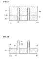
- the supporting member 100 has, on the second principal surface 11b of the supporting substrate 11, a plurality of device arrangement regions 101, 102 in which the electronic device 6 is arranged by the projecting portion 13a of the through electrode 13.
- the number of the electronic devices 6 that are arranged in each device arrangement region 101, 102 may be the same or may differ between the regions. Also, the number of electronic devices 6 that are arranged in each device arrangement region 101, 102 may be one or may be plural. It is also possible to mount an electronic device 110 on the circuit 14 on the first principal surface 11a side of the supporting substrate 11 of the supporting member 100.
- the electronic device mounting structure shown in FIG. 15 has a protective layer 8 that contains the electronic device 6 within itself. Thereby, it is possible to realize a semiconductor package.
- the protective layer 8 using, for example, an insulating resin (mold resin), a substrate with a cavity and the like, it is not particularly limited to these.
- the protective layer 8 when performing mounting of the electronic device 6 and formation of the protective layer 8 prior to forming the circuit 14 and the connection terminal 15 on the first principal surface 1a side of the supporting member, it is possible to make the package thinner by grinding the first principal surface 1a side of the supporting substrate 11 and using this protective layer 8 as a support body. In this case, after grinding the first principal surface side 1a, it is possible to provide the circuit 14 and the connection terminal 15 as required.
- FIG. 16 shows an example of the pad arrangement of the device substrate 1 that is used for the electronic device 6 in each of the aforementioned embodiments.
- the pad 5 is formed on the periphery of each of the through holes 2 that are formed on the principal surface 1b of the device substrate 1.
- the circuit 4 shown in FIG. 1A is omitted in the illustration of FIG. 16 .
- the arrangement of the through hole 2 and the pad 5 can be suitably designed, and the projecting portion is arranged on the supporting member in conformity with this arrangement.
- FIG. 16 shows the device substrate 1 that has twelve through holes 2.
- the number of the projecting portions 13a of the supporting member may be the same number of through holes 2, or may be a fewer number to omit insertion into some of the through holes 2.
- the dimensions of the through hole 2 and each portion at its periphery are not particularly limited.
- the outer diameter of the projecting portion 13a is, for example, 60 ⁇ m
- the inner diameter of the through hole 2 is, for example, 80 ⁇ m
- the I/O pad 5 is a 100 ⁇ m square (100 ⁇ m ⁇ ).
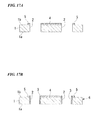
- FIG. 17A to FIG. 17D schematically show an example of steps of processing the device substrate 1 to mount on the supporting member 10.
- the exposed portion of the device substrate 1 is removed to penetrate the through hole 2 from the principal surface 1b to the principal surface 1a, whereby it is possible to form the through hole 2 in the device in which the through hole 2 is not formed.
- the removal of the pad 5 material in the case of being, for example, Al, is performed by wet etching using a chemical solution.
- the removal of the device substrate 1, in the case of being, for example, Si, is performed by the aforementioned Bosch process.
- back surface grinding is performed after forming a bottomed hole from the principal surface 1b side with a certain amount of depth (a blind via), and so when the hole reaches the principal surface 1a, penetration can be achieved.
- the depth of the blind via is not particularly limited, but as a concrete example, the depth of the blind via is, for example, 70 ⁇ m, and the device substrate 1 is thinned to a thickness of 50 ⁇ m by the back surface grinding.
- the insulating layer 3 is formed on the inner wall of the through hole 2.
- methods of film formation include a plasma chemical vapor deposition method that uses tetraethoxysilane (TEOS) as a raw material, a plasma chemical vapor deposition method that uses silane (SiH 4 ) or the like, and thermal oxidation of Si.
- TEOS tetraethoxysilane
- SiH 4 silane
- the material of the insulating layer 3 is not limited to SiO 2 , and may be other insulating materials, such as silicon nitride (SiN) or insulating resin.
- the projecting portion 13a of the through electrode 13 of the support member 10 is inserted into the through hole 2 in which the insulating layer 3 has been formed on the inner wall, and the electronic device 6 is arranged on the second principal surface 11b of the supporting substrate 11.
- an adhesive layer or insulating layer may be provided as necessary between the second principal surface 11b and the first principal surface 1a of the device substrate 1.
- the I/O pad 5 of the electronic device electronic device 6 and the projecting portion 13a of the through electrode 13 are electrically connected.
- an electrically conductive bonding material 7 such as solder or conductive paste.
- the electrically conductive bonding material 7 is applied to only the portion in the vicinity of the pad 5, but it may be applied to the entire through hole 2.
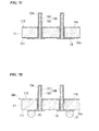
- FIG. 18A is a cross-sectional view that schematically shows an example of the state of a layered arrangement of the electronic devices 6 using the supporting member 19 in which a layer of solder 18 is provided on the projecting portion 13a
- FIG. 18B is a cross-sectional view that schematically shows an example of an electronic device mounting structure that is manufactured using the electronic devices that have been arranged in a layered manner as shown in FIG. 18A
- This supporting member 19 corresponds to one in which the outer layer 131 in the supporting member 10B of the fourth embodiment shown in FIG. 8B is replaced with the layer of solder 18.
- the material with which the inner side of the layer of solder 18 is filled may be a conductor or may be an insulator. Also, in the example shown in FIGS.
- the layer of solder 18 is formed also inside the through hole 12 of the supporting member 19, but the layer of solder 18 may be provided only on the projecting portion 13a of the through electrode 13 that is formed by a conductor.
- a method of providing the layer of solder 18 only on the projecting portion 13a includes manufacturing the supporting member 10 shown in FIG. 1B , and then forming the layer of solder 18 by further application of solder paste.
- the connecting terminal 15 that is provided on the supporting member 19 being a solder bump
- the present invention can be suitably utilized for mounting an electronic device on a semiconductor chip.
Landscapes
- Internal Circuitry In Semiconductor Integrated Circuit Devices (AREA)
- Printing Elements For Providing Electric Connections Between Printed Circuits (AREA)
Abstract
Description
- The present invention relates to an electronic device mounting structure for mounting an electronic device such as a semiconductor chip on a support member such as an interposer, and to a method of mounting the electronic device.
Priority is claimed on Japanese Patent Application No.2009-098035, filed April 14, 2009 - With the increasing sophistication of electrical equipment such as mobile phones in recent years, there is a demand for further increases in the speed and performance of electronic devices that are used in the equipment. In order to meet these demands, technical development is required not only to increase the speed of the device itself through miniaturization and the like, but also to increase the speed and density of the package of the device.
As technologies that achieve high-density mounting of electronic devices, research and development of various through-electrode formation technologies and through-wiring substrate formation technologies have been actively advanced. For example, three-dimensional stacking technology that laminates and mounts chips using through wiring and System in Package (SiP) technology that uses a through wiring substrate having through electrodes formed therein have been proposed. -
Patent Document 1 discloses a substrate having a through electrode that is fabricated from a silicon wafer having an embedded insulating layer between a supporting substrate layer and a silicon layer. In this substrate having a through electrode, a blind via hole is formed reaching the silicon layer to a depth that allows formation of a recess. An inner wall insulating layer is applied onto the blind via hole to form a conductive layer. Then, by removing the silicon layer, the portion of the conductive layer corresponding to the recess is exposed as a wafer outer raised portion. -
Patent Document 2 discloses a method for manufacturing a semiconductor device that includes: laminating three or more semiconductor chips which each have a terminal with two ends projecting from a substrate, on an interposer; positioning the semiconductor chips and the interposer so as to align the adjacent terminals with each other; and bonding the adjacent terminals together in a lot. -
- [Patent Document 1] Japanese Unexamined Patent Application, First Publication No.
2005-93954 - [Patent Document 2] Japanese Unexamined Patent Application, First Publication No.
2003-282819 - In order to achieve further increases in the speed and density of an apparatus on which an electronic device is mounted, it is necessary to ensure a low-resistance electrical connection between the top of the supporting member, such as an interposer, and the semiconductor chip, or among the laminated semiconductor chips. In order to secure such a low-resistance electrical connection, high positional accuracy between the terminals and reduced resistance of the joined portions between terminals are needed. In conventional mounting technology, in order to prevent position gaps of the opposing terminals between substrates, various position control measures are taken. However, in order to realize a much more high density assembly, it is desired to be able to directly observe the terminal positions on the lower side substrate during the semiconductor chip lamination work.
- The present invention was achieved in view of the above circumstances, and has an object of providing an electronic device mounting structure and an electronic device mounting method that make it possible to easily mount an electronic device such as a semiconductor chip on a support member such as an interposer.
- In order to solve the aforementioned issues, the present invention employs the following. In particular, an electronic device mounting structure according to a first aspect of the present invention includes: a supporting member that includes a supporting substrate, and a through electrode that penetrates the supporting substrate from a first principal surface that is one principal surface of the supporting substrate to a second principal surface that is the other principal surface, and that includes a projecting portion that projects from the second principal surface; and an electronic device that includes a device substrate on which a circuit is formed, and a through hole that penetrates between both principal surfaces of the device substrate, wherein the electronic device is arranged on the second principal surface of the supporting substrate so that the projecting portion of the supporting member is inserted into the through hole, and the circuit of the electronic device is electrically connected with the projecting portion.
It may be arranged such that the electronic device mounting structure includes a plurality of the electronic devices, wherein each of the electronic devices is laminated on the second principal surface of the supporting substrate.
It may be arranged such that the supporting member includes, on the second principal surface of the supporting substrate, a plurality of device arrangement regions in which the electronic devices are arranged by the projecting portion.
It may be arranged such that the electronic device mounting structure further includes a protective layer that includes the electronic devices within itself.
It may be arranged such that a layer of solder is formed on the outer periphery surface of the projecting portion over the entire length of the projecting portion, and the circuit of the electronic device and the projecting portion are electrically connected by solder that is melted out from the layer of solder.
It may be arranged such that the supporting member includes a connection terminal on the first principal surface side.
An electronic device according to a second aspect of the present invention includes the above-described electronic device mounting structure. - Further, an electronic device mounting method according to a third aspect of the present invention includes: a first step of preparing a supporting member including a supporting substrate, and a through electrode that penetrates the supporting substrate from a first principal surface that is one principal surface of the supporting substrate to a second principal surface that is the other principal surface, and that includes a projecting portion that projects from the second principal surface; a second step of preparing an electronic device that includes a device substrate, and a through hole that penetrates between both principal surfaces of the device substrate; and a third step of arranging the electronic device on the second principal surface of the supporting substrate so that the projecting portion of the supporting member is inserted into the through hole of the electronic device, and electrically connecting the circuit of the electronic device and the projecting portion.
- It may be arranged such that the first step includes: a step of laminating, on the second principal surface of the supporting substrate, a projecting portion formation auxiliary layer having a thickness greater than the height of the projecting portion; a step of forming a through hole that penetrates from the first principal surface to the second principal surface of the supporting substrate; a step of forming a communication hole extending from the through hole of the supporting substrate to reach the interior of the projecting portion formation auxiliary layer; a step of filling with a conductor the through hole of the supporting substrate and the communication hole; and a step of exposing the second principal surface of the supporting substrate by removing the projecting portion formation auxiliary layer, and forming a through electrode that consists of the conductor, penetrates the supporting substrate from the first principal surface to the second principal surface, and includes the projecting portion that projects from the second principal surface.
It may be arranged such that the first step includes: a step of farming a hole in a base material that has a thickness greater than the sum of the thickness of the supporting substrate and the height of the projecting portion from a surface that becomes the first principal surface of the supporting substrate; a step of filling the hole with a conductor; and a step of forming the second principal surface of the supporting substrate by removing a portion of the base material from the opposite side of the first principal surface of the base material until a portion of the conductor is exposed, and forming a through electrode that consists of the conductor, penetrates the supporting substrate from the first principal surface to the second principal surface, and includes the projecting portion that projects from the second principal surface.
It may be arranged such that the first step includes a step of forming a layer of solder on the outer periphery surface of the projecting portion over the entire length of the projecting portion, and the third step includes a step of inserting the projecting portion of the supporting member into each through hole of a plurality of the electronic devices to arrange the electronic devices in a layered manner on the second principal surface of the supporting substrate, and a step of electrically connecting all at once each circuit of the plurality of electronic devices and the projecting portion by melting the layer of solder. - According to the present invention, even after the projecting portion of the support member has been inserted into each through hole of the plurality of electronic devices, it is possible to confirm the position of the projecting portion from above the electronic device. Therefore, high-density mounting of the electronic devices can be easily performed. In addition, since the projecting portion is a unit conductor that is continuous in the lengthwise direction, even if a plurality of electronic devices are mounted in a layered manner, no joining portion will be present between the electronic devices. As a result, it is possible to achieve a lower resistance of the electrical connections among the electronic devices and the reduction of the total thickness of the layered electronic devices.
-
-
FIG. 1A is a cross-sectional view that schematically shows the electronic device mounting structure according to the first embodiment of the present invention. -
FIG. 1B is a cross-sectional view that schematically shows one example of the supporting member that is used in the electronic device mounting structure according to the embodiment. -
FIG. 2A is a cross-sectional view that schematically shows the first stage, among the manufacturing steps of the supporting member ofFIG. 1B andFIG. 6B . -
FIG. 2B is a cross-sectional view that schematically shows the stage followingFIG. 2A . -
FIG. 2C is a cross-sectional view that schematically shows the stage followingFIG. 2B . -
FIG. 2D is a cross-sectional view that schematically shows the stage followingFIG. 2C . -
FIG 3A is a cross-sectional view that schematically shows the stage followingFIG. 2D , among the manufacturing steps of the supporting member ofFIG. 1B . -
FIG. 3B is a cross-sectional view that schematically shows the stage followingFIG. 3A . -
FIG. 3C is a cross-sectional view that schematically shows the stage followingFIG. 3B . -
FIG. 3D is a cross-sectional view that schematically shows the stage followingFIG. 3C . -
FIG. 4A is a cross-sectional view that schematically shows the electronic device mounting structure according to the second embodiment of the present invention. -
FIG. 4B is a cross-sectional view that schematically shows an example of the supporting member that is used in the electronic device mounting structure according to the embodiment. -
FIG. 5A is a cross-sectional view that schematically shows the first stage, among the manufacturing steps of the supporting member ofFIG. 4B . -
FIG. 5B is a cross-sectional view that schematically shows the stage followingFIG.5A . -
FIG. 5C is a cross-sectional view that schematically shows the stage followingFIG. 5B . -
FIG. 5D is a cross-sectional view that schematically shows the stage followingFIG. 5C . -
FIG. 6A is a cross-sectional view that schematically shows the electronic device mounting structure according to the third embodiment of the present invention. -
FIG. 6B is a cross-sectional view that schematically shows an example of the supporting member that is used in the electronic device mounting structure according to the embodiment. -
FIG. 7A is a cross-sectional view that schematically shows the stage that followsFIG. 2D , among the manufacturing steps of the supporting member ofFIG. 6B . -
FIG. 7B is a cross-sectional view that schematically shows the stage followingFIG. 7A . -
FIG. 7C is a cross-sectional view that schematically shows the stage followingFIG. 7B . -
FIG. 7D is a cross-sectional view that schematically shows the stage followingFIG. 7C . -
FIG. 8A is a cross-sectional view that schematically shows the electronic device mounting structure according to the fourth embodiment of the present invention. -
FIG. 8B is a cross-sectional view that schematically shows one example of the supporting member that is used in the electronic device mounting structure according to the embodiment. - In
FIG. 9A , (a) is a cross-sectional view that schematically shows the first stage, among the manufacturing steps of the supporting member ofFIG. 8B , while (b) is an arrow view of a portion of (a) seen from below, serving as an explanatory view that shows the shape of the throughhole 12 and thecore 17. -
FIG. 9B is a cross-sectional view that schematically shows the stage followingFIG. 9A . -
FIG. 9C is a cross-sectional view that schematically shows the stage followingFIG. 9B . -
FIG. 10A is a cross-sectional view that schematically shows the stage followingFIG. 9C , among the manufacturing steps of the supporting member ofFIG. 8B . -
FIG. 10B is a cross-sectional view that schematically shows the stage followingFIG. 10A . -
FIG. 10C is a cross-sectional view that schematically shows the stage followingFIG. 10B . -
FIG. 11A is a cross-sectional view that schematically shows the stage followingFIG. 10C , among the manufacturing steps of the supporting member ofFIG. 8B . -
FIG. 11B is a cross-sectional view that schematically shows the stage followingFIG. 11A . -
FIG. 11C is a cross-sectional view that schematically shows the stage followingFIG. 11B . -
FIG. 11D is a cross-sectional view that schematically shows the stage followingFIG. 11C . -
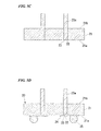
FIG. 12 is a cross-sectional view that schematically shows a modified example of the supporting member that is used in the electronic device mounting structure of the present invention. -
FIG. 13 is a cross-sectional view that schematically shows a modified example of the supporting member that is used in the electronic device mounting structure of the present invention. -
FIG. 14 is a cross-sectional view that schematically shows one aspect that has a plurality of device arrangement regions in the electronic device mounting structure of the present invention. -
FIG. 15 is a cross-sectional view that schematically shows one aspect that has a protective layer that includes the electronic device within itself in the electronic device mounting structure of the present invention. -
FIG. 16 is a plan view that schematically shows an example of the pad arrangement on the device substrate. -
FIG. 17A is a cross-sectional view that schematically shows the first stage, among the steps of processing the device substrate to mount it on the supporting member. -
FIG. 17B is a cross-sectional view that schematically shows the stage followingFIG. 17A . -
FIG. 17C is a cross-sectional view that schematically shows the stage followingFIG. 17B . -
FIG. 17D is a cross-sectional view that schematically shows the stage followingFIG. 17C . -
FIG. 18A is a cross-sectional view that schematically shows an example of the state of the electronic devices being in a layered arrangement using the support member in which a layer of solder is provided on the projecting portion. -
FIG. 18B is a cross-sectional view that schematically shows an example of the electronic device mounting structure that is manufactured using the electronic devices that are arranged in a layered manner as shown inFIG. 18A . - Hereinbelow the preferred embodiments of the present invention shall be described with reference to the drawings.
FIG. 1A to FIG. 3D show the electronic device mounting structure and mounting method using a supportingmember 10, according to a first embodiment of the present invention.
The supportingmember 10 shown inFIGS. 1A and 1B is a supporting member that includes a supportingsubstrate 11, and a throughelectrode 13 that penetrates the supportingsubstrate 11 from a firstprincipal surface 11a that is one principal surface of the supportingsubstrate 11 to a secondprincipal surface 11b that is the other principal surface, and includes a projectingportion 13a that projects from the secondprincipal surface 11b, in order to mount anelectronic devices 6 on the secondprincipal surface 11b side. This supportingmember 10 may further include aconnection terminal 15 such as a solder bump on the firstprincipal surface 11a side, and is capable of electrically connecting thecircuit 4 of theelectronic device 6, and an external substrate (not shown), such as a printed circuit board, via the throughelectrode 13, thecircuit 14 and theconnection terminal 15. - In the case of the present embodiment, the supporting
substrate 11 consists of a semiconductor substrate, such as a silicon (Si) substrate. Insulatinglayers principal surfaces hole 12, and thereby provide insulation between thecircuit 14 and the semiconductor substrate and between the throughelectrode 13 and the semiconductor substrate. In the case ofFIG. 1A and FIG. 1B , the insulatinglayer 111 is formed as a continuous layer from the firstprincipal surface 11a of the supportingsubstrate 11 to the inner wall of the throughhole 12, but separate insulating layers may be formed on the firstprincipal surface 11a of the supportingsubstrate 11 and the inner wall of the throughhole 12. - The
electronic device 6 that is used in the present embodiment is a semiconductor chip that has adevice substrate 1, and a throughhole 2 that penetrates bothprincipal surfaces device substrate 1. In the case of using a semiconductor chip, thedevice substrate 1 is a semiconductor substrate such as a silicon (Si) substrate, and it is preferable to provide aninsulating layer 3 on the inner wall of the throughhole 2 in order to provide insulation between the projectingportion 13a of the throughelectrode 13 and the semiconductor substrate.
Thecircuit 4 that constitutes the electronic device is formed on theprincipal surface 1b of thedevice substrate 1. It is possible to constitute a portion of thecircuit 4 as a semiconductor circuit. The type of electronic device is not particularly limited, and examples include a memory device or sensor device.
Apad 5 that is connected to thecircuit 4 is formed at the periphery of the throughhole 2. Thepad 5 and the projectingportion 13a are electrically connected by an electricallyconductive bonding material 7 such as solder or conductive paste. - As shown in
FIG. 1A , theelectronic device 6 is arranged on the secondprincipal surface 11b of the supportingsubstrate 11 so that the projectingportion 13a of the supportingmember 10 is inserted into the throughhole 2 of theelectronic device 6. In addition, thecircuit 4 of theelectronic device 6 and the projectingportion 13a are electrically connected. By layering a plurality of theelectronic devices 6 so that the projectingportion 13a is inserted into each throughhole 2 of the plurality ofelectronic devices 6, multi-layering of theelectronic devices 6 can be achieved. - Moreover, electronic circuit components such as resistors, capacitors, and inductors may be provided on the
circuit 14 of the supportingmember 10. Also, in the case of the supportingsubstrate 11 consisting of a semiconductor substrate, a semiconductor circuit may be formed on the supportingsubstrate 11. - According to the electronic device mounting structure of the present embodiment, even after the projecting
portion 13a has been inserted into each through hole of the plurality ofelectronic devices 6, it is possible to confirm the position of the projectingportion 13a from above theelectronic devices 6. Therefore, high-density mounting of theelectronic devices 6 can be easily performed. Also, since the projectingportion 13a is a unit conductor that is continuous in the lengthwise direction, even if a plurality ofelectronic devices 6 are mounted in a layered manner, no joining portion will be present between theelectronic devices 6. As a result, it is possible to achieve lower resistance of the electrical connections among theelectronic devices 6 and reduction of the total thickness of the layeredelectronic devices 6. - It is possible to manufacture the supporting
member 10 of the present embodiment by the manufacturing method shown inFIG. 2A to FIG. 2D , andFIG. 3A to FIG. 3D .
First, as shown inFIG. 2A , a projecting portion formationauxiliary layer 16 is laminated on the secondprincipal surface 11b side of the supportingsubstrate 11, and the throughhole 12 is formed that penetrates from the firstprincipal surface 11a of the supportingsubstrate 11 to the secondprincipal surface 11b. The thickness of the projecting portion formationauxiliary layer 16 is greater than the height of the projectingportion 13a that is provided on the supportingmember 10. - In the case of the present embodiment, the supporting
substrate 11 is a silicon substrate, the projecting portion formationauxiliary layer 16 is a silicon layer, and an embedded insulatinglayer 112 is provided therebetween. In addition, following the throughhole 12, as shown inFIG. 2B , ahole 113 is formed in the embedded insulatinglayer 112.
It is possible to use an SOI substrate as the Si/SiO2/Si layered product. The dimensions of each layer are not particularly limited, and may be suitably determined in accordance with the intended purpose of the supportingmember 10. As a concrete example, the thickness of the supportingsubstrate 11 is, for example, 150 µm, the thickness of the projecting portion formationauxiliary layer 16 is, for example, 200 µm, the height of the projectingportion 13a is, for example, 180 µm, and the diameter of the through hole 12 (corresponding to the outer diameter of the projectingportion 13a) is, for example, 60 µm. - Methods of forming a hole in Si include a Bosch process that alternately performs Si etching by a high-density plasma using SF6 gas, and passivation film formation on the side wall of the hole using C4F8 gas or the like. It is also possible to employ dry etching techniques other than the Bosch process, wet etching using a chemical solution, and physical processing by a laser or the like.
Methods of forming a hole in SiO2 include dry etching using CF4 gas or the like, wet etching using a chemical solution, and physical processing by a laser or the like. - Next, as shown in
FIG. 2C , acommunication hole 16a is formed extending from the throughhole 12 so as to reach the interior of the projecting portion formationauxiliary layer 16. The depth of thecommunication hole 16a in the projecting portion formationauxiliary layer 16 is substantially the same as the height of the projectingportion 13a.
Next, as shown inFIG. 2D , the insulatinglayer 111 is formed on the inner wall of the through-hole 12, and the firstprincipal surface 11a of the supportingsubstrate 11. Note that the formation (existence) of the insulatinglayer 111 is discretionary, and it may be performed as needed. For example, if it is an insulating layer that consists of SiO2, it will be obtained by the plasma chemical vapor deposition method that uses tetraethoxysilane (TEOS) as a raw material, the plasma CVD method that uses silane (SiH4) or the like, and thermal oxidation of Si. The material of the insulating layer is not limited to SiO2, and may be other insulating materials, such as silicon nitride (SiN) or insulating resin. The insulatinglayer 111 can also be continuously formed on the inner wall of thecommunication hole 16a. Note that thereference numeral 114 in the drawing distinguishes the insulatinglayer 111 in thecommunication hole 16a. - Next, as shown in
FIG. 3A , the through-hole 12 and thecommunication hole 16a are filled with aconductor 13. The throughelectrode 13 which has the projectingportion 13a is constituted by thisconductor 13.
As theconductor 13, metals such as copper (Cu) and tungsten (W), alloys such as Au-Sn, and nonmetallic conductors such as polysilicon, can be used. As the filling method, it is possible to suitably apply a plating method, a sputtering method, a molten metal filling method, chemical vapor deposition, and the like. - Next, as shown in
FIG. 3B , the projecting portion formationauxiliary layer 16 is completely removed. That is, the entire surface of the secondprincipal surface 11b (in greater detail, the insulating layer 112) of the supportingsubstrate 11 is exposed. When the projecting portion formationauxiliary layer 16 consists of Si, methods of removal include dry etching using SF6 gas and the like as well as wet etching using a chemical solution. - When the insulating
layer 114 has been formed also in the interior of thecommunication hole 16a inFIG. 2D , as shown inFIG. 3C , the insulatinglayer 114 on the surface of the projectingportion 13a is removed. When the insulatinglayer 114 consists of SiO2, methods of removal include dry etching using CF4 gas and the like as well as wet etching using a chemical solution.
When removing the insulatinglayer 114 from the surface of the projectingportion 13a, in order to protect the insulatinglayer 112 on the secondprincipal surface 11b, it is preferable to form a protective layer, such as a resist layer, on the insulatinglayer 112 in advance. Alternatively, it may be arranged such that the thickness of the insulatinglayer 112 is made thicker beforehand so that the insulatinglayer 112 with a sufficient thickness remains even if removal of the insulatinglayer 114 is completed. In this case, the insulatinglayer 114 on the projectingportion 13a surface can be removed without forming a protective layer, such as a resist layer. - Then, as shown in
FIG. 3D , thecircuit 14 that is electrically connected with the throughelectrode 13, and theconnection terminal 15 such as a solder bump that is electrically connected with thecircuit 14 are formed on the firstprincipal surface 11a side of the supportingsubstrate 11. Thereby, the supportingmember 10 of the present embodiment is completed. -
FIG. 4A to FIG. 5D show the electronic device mounting structure and mounting method using a supportingmember 20 according to the second embodiment of the present invention.
In the case of the present embodiment, a supportingsubstrate 21 consists of an insulating substrate, such as a glass substrate.
In the same manner as the above-mentioned first embodiment, the supportingmember 20 has a supportingsubstrate 21, and a throughelectrode 23 that penetrates the supportingsubstrate 21 from a firstprincipal surface 21a to a secondprincipal surface 21b, and has a projectingportion 23a that projects from the secondprincipal surface 21b, with theelectronic device 6 mounted on the secondprincipal surface 21b side. In the case of the present embodiment, as shown inFIG. 4A and FIG. 4B , since the supportingsubstrate 21 does not conduct with the throughelectrode 23 and thecircuit 24, there is no need to provide an insulating layer on theprincipal surfaces hole 22. - The
electronic device 6 is arranged on the secondprincipal surface 21b so that the projectingportion 23a of the supportingmember 20 is inserted into a through-hole 2. Moreover, thecircuit 4 of theelectronic device 6 and the projectingportion 23a are electrically connected. By stacking a plurality of theelectronic devices 6 so that the projectingportion 23a is inserted into each throughhole 2 of the plurality ofelectronic devices 6, multi-layering of theelectronic devices 6 can be achieved.
Moreover, the supportingmember 20 has aconnection terminal 25 such as a solder bump on the firstprincipal surface 21a side, and is capable of electrically connecting thecircuit 4 of theelectronic device 6 and an external substrate (not shown) such as a printed circuit board, via the throughelectrode 23, thecircuit 24 and the and theconnection terminal 25.
It is also possible to provide electrical components such as resistors, capacitors, and inductors on thecircuit 24 of the supportingmember 20. - According to the electronic device mounting structure of the present embodiment, even after the projecting
portion 23a has been inserted into each throughhole 2 of the plurality ofelectronic devices 6, it is possible to confirm the position of the projectingportion 23a from above theelectronic devices 6. Therefore, high-density mounting of theelectronic devices 6 can be easily performed. Moreover, since the projectingportion 23a is a unit conductor that is continuous in the lengthwise direction, even if a plurality ofelectronic devices 6 are mounted in a layered manner, no joining portion will be present between theelectronic devices 6. As a result, it is possible to achieve a reduction in the resistance of the electrical connections among theelectronic devices 6 and reduction of the total thickness of the layeredelectronic devices 6.
Further, according to the present embodiment, since the supportingsubstrate 21 consists of an insulator, it is not necessary to form an insulating layer on the substrate surface and inner wall of the through hole. As a result, it is possible to simplify the manufacturing process. - The supporting
member 20 of the present embodiment can be manufactured by the method shown, for example, inFIG. 5A to FIG. 5D .
First, as shown inFIG. 5A , abase material 26 that has a larger thickness than the sum of the thickness of the supportingsubstrate 21 and the height of the projectingportion 23a of the supportingmember 20 after completion is prepared, and ahole 26a is formed from the side that becomes the firstprincipal surface 21a of the supportingsubstrate 21. The depth of thehole 26a is (substantially) equal to the sum of the thickness of the supportingsubstrate 21 and the height of the projectingportion 23a.
The dimensions of each portion are not particularly limited and can be suitably determined according to the application of the supportingmember 20. As a concrete example, the thickness of the supportingsubstrate 21 is, for example, 150 µm, the thickness of thebase material 26 is, for example, 500 µm, the depth of thehole 26a is, for example, 320 µm, and the diameter of thehole 26a is, for example, 60 µm. - A method of forming the a
fine hole 26a in theglass base material 26 includes a method that modifies the portion of the glass which serves as thehole 26a by femtosecond laser irradiation, and then removes that modified portion by wet etching, as disclosed in Japanese Unexamined Patent Application, First Publication No.2006-303360 hole 26a may also be formed by dry etching that uses gas or the like, wet etching that uses a chemical solution, and physical processing by a laser or the like. - Next, as shown in
FIG. 5B , the communication holes 26 are filled with aconductor 23. The throughelectrode 23 which has the projectingportion 23a is constituted by thisconductor 23.
As theconductor 23, metals such as copper (Cu) and tungsten (W), alloys such as Au-Sn, and nonmetallic conductors such as polysilicon, can be used. As the filling method, it is possible to suitably apply a plating method, a sputtering method, a molten metal filling method, chemical vapor deposition, and the like. - Then, as shown in
FIG. 5C , by removing a portion of the base material from the opposite side of the firstprincipal surface 21a of thebase material 26 until a portion of theconductor 23 is exposed, the secondprincipal surface 21b of thesupport substrate 21 is formed, and by theconductor 23 that fills thehole 26a, the throughelectrode 23 is formed that penetrates the supportingsubstrate 21 from the firstprincipal surface 21a to the secondprincipal surface 21b, and has the projectingportion 23a that projects from the secondprincipal surface 21b.
Methods of glass removal include dry etching using gas or the like, and wet etching using a chemical solution such as hydrofluoric acid (HF). - Then, as shown in
FIG. 5D , thecircuit 24 that is electrically connected with the throughelectrode 23, and theconnection terminal 25 such as a solder bump that is electrically connected with thecircuit 24 are formed on the firstprincipal surface 21a side of the supportingsubstrate 21. Thereby, the supportingmember 20 of the present embodiment is completed. -
FIG. 6A to FIG. 7D show the electronic device mounting structure and mounting method using a supportingmember 10A according to the third embodiment of the present invention.
In the case of the present embodiment, the throughelectrode 13A that has the projectingportion 13a consists of a plurality of layers (specifically, two layers consisting of anouter layer 131 and an inner layer 132). Here, theouter layer 131 is constituted from a conductor, and is electrically connected with thecircuit 4 of theelectronic device 6. In addition, theouter layer 131 and thecircuit 14 are formed as a continuous conductor layer. The material of theinner layer 132 may be a conductor or an insulator. Further, theinner layer 132 is included in theouter layer 131 at the distal end of the projectingportion 13a.
The electronic device mounting structure of the present embodiment can exhibit the same function effect as the aforementioned first embodiment. - The supporting
member 10A of the present embodiment can be manufactured by the manufacturing method shown, for example, inFIG. 2A to FIG. 2D , and subsequentlyFIG. 7A to FIG. 7D . Here, the steps shown inFIG. 2A to FIG. 2D can be performed in the same manner as the first embodiment, so overlapping descriptions shall be omitted. - In
FIG. 7A , aconductor 131 is applied inside the throughholes 12 and thecommunication holes 16a formed inFIG. 2A to FIG. 2D . The aforementionedouter layer 131 is constituted by thisconductor 131. Moreover, in the case of the present embodiment, simultaneously with the applying of theouter layer 131, thecircuit 14 is formed on the insulatinglayer 111 by the same conductor. Note that thecircuit 14 may also be formed a separate step from theouter layer 131. Further, thecircuit 14 may be formed with a different material than theouter layer 131. - As the conductor that constitutes the
outer layer 131 and thecircuit 14, metals such as copper (Cu) and tungsten (W), alloys such as Au-Sn and solder, and nonmetallic conductors such as polysilicon, can be used. As the applying method, it is possible to suitably apply a plating method, a sputtering method, a molten metal filling method, chemical vapor deposition, and the like. - Next, as shown in
FIG. 7B , further to the inner side of theconductor 131 that has been applied inside the inner wall of the throughhole 12 and thecommunication hole 16a, theinner layer 132 is applied. The filling material of theinner layer 132 may be a conductor or it may be an insulator. For example, in the case of applying an insulating resin by vacuum printing for filling, it is possible to impart a certain degree of flexibility to the throughelectrode 13A that has the projectingportion 13a, and so it is possible to relieve the stress that occurs during mounting of theelectronic device 6. Note that the filling material of theinner layer 132 is not limited to insulating resin, and may be another insulator or even a conductor such as metal. As the filling method, it is possible to suitably apply a plating method, a sputtering method, or chemical vapor deposition in accordance with the material. - Next, as shown in
FIG. 7C , the projecting portion formationauxiliary layer 16 is completely removed. Moreover, when the insulatinglayer 111 has been formed also in the interior of thecommunication hole 16a inFIG. 2D , the insulatinglayer 111 of the projectingportion 13a surface is removed. Thereafter, as shown inFIG. 7D , aconnection terminal 15 such as a solder bump that is electrically connected with thecircuit 14 is formed on the firstprincipal surface 11a side of the supportingsubstrate 11. Thereby, the supportingmember 10A of the present embodiment is completed. For these steps, it is possible to use the same methods as those described in the first embodiment withFIGS. 3B ,3C, and 3D , so overlapping descriptions will be omitted. Note that although not particularly illustrated, the formation step of thecircuit 14 can also be performed by the step shown inFIG. 7D .
The supportingmember 10A that is obtained by the present embodiment has a structure in which theinner layer 132 is included within theouter layer 131 at the distal end of the projectingportion 13a. -
FIG. 8A to FIG. 11D show the electronic device mounting structure and mounting method using the supportingmember 10B according to the fourth embodiment of the present invention.
In the case of the present embodiment, the throughelectrode 13B that has the projectingportion 13a consists of a plurality of layers (specifically, two layers consisting of theoutside layer 131 and the inside layer 132). Here, theouter layer 131 is constituted from a conductor, and is electrically connected with theelectronic device 6 and thecircuit 4. Also, theouter layer 131 and thecircuit 14 are formed as a continuous conductor layer. The material of theinner layer 132 may be a conductor or an insulator. Also, the throughelectrode 13B has a layer structure in which theinner layer 132 is exposed from the outer later 131 at the distal end of the projectingportion 13a.
According to the electronic device mounting structure of the present embodiment, it is possible to exhibit the same function effect of the first and third embodiments described above. - The supporting
member 10B of the present embodiment can be manufactured by the manufacturing method shown, for example, inFIGS. 9A to 9C ,FIGS. 10A to 10C , andFIGS. 11A to 11D .
InFIG. 9A , as shown in (a), the starting material in which the projecting portion formationauxiliary layer 16 is laminated on the secondprincipal surface 11b side of the supporting substrate 11 (in greater detail, on the insulating layer 112) is the same as the first embodiment described above (for example, an SOI substrate). Note that the throughhole 12 that penetrates the supportingsubstrate 11 from the firstprincipal surface 11a to the secondprincipal surface 11b differs from that inFIG. 2A on the point of having a cross-sectional donut shape as shown in (b) ofFIG. 9A , that is, it has a core 17 consisting of the material of the supportingsubstrate 11 remaining in the center portion of the throughhole 12.
As a concrete example of the dimensions of each portion, the thickness of the supportingsubstrate 11 is, for example, 150 µm, the thickness of the projecting portion formationauxiliary layer 16 is, for example, 200 µm, the height of the projectingportion 13a is, for example, 180 µm, the outer diameter of the throughhole 12 is, for example, 60 µm, and the inner diameter of the through hole 12 (that is, the outer diameter of the core 17) is, for example, 30 µm. - Following the through
hole 12, as shown inFIG. 9B , ahole 113 is also formed in the embedded insulatinglayer 112. Moreover, as shown inFIG. 9C , acommunication hole 16a that reaches the interior of the projecting portion formationauxiliary layer 16 is formed extending from the throughhole 12. Thehole 113 and thecommunication hole 16a both have a cross-sectional ring shape, that is, have the core 17 that consists of the remaining material of the embedded insulatinglayer 112 and the projecting portion formationauxiliary layer 16.
The depth of thecommunication hole 16a in the projecting portion formationauxiliary layer 16 is substantially the same as the height of the projectingportion 13a. - As shown in
FIG. 10A , the insulatinglayer 111 is formed on the inner wall of the through-hole 12 (including the outer wall of the core 17) and the firstprincipal surface 11a of the supportingsubstrate 11. Note that the formation of the insulatinglayer 111 is discretionary, and it may be performed as needed. The formation of the insulatinglayer 111 can be performed in the same manner as the formation of the insulatinglayer 111 shown inFIG. 2D of the first embodiment, for example. - Subsequently, as shown in
FIG. 10B , the through-hole 12 and thecommunication hole 16a are filled with aconductor 131. The aforementionedouter layer 131 is constituted by thisconductor 131. As theconductor 131 used for theouter layer 131, metals such as copper (Cu) and tungsten (W), alloys such as Au-Sn and solder, and nonmetallic conductors such as polysilicon, can be used. As the filling method, it is possible to suitably apply a plating method, a sputtering method, a molten metal filling method, chemical vapor deposition, and the like. - Then, as shown in
FIG. 10C , the insulatinglayer 111 inside the outer layer 131 (that is, on the outer wall of the core 17) and the core 17 are removed. This removal is performed after carrying out necessary protection of the insulatinglayer 111 that is on the outer side of the outer layer 131 (on the inner wall of the throughhole 12 and thecommunication hole 16a and on the firstprincipal surface 11a). In the case of the starting material being an SOI substrate, Si and SiO2 are removed by, for example, SF6 gas, CF4 gas or the like. It is also possible to use another method.
Methods of protecting the insulatinglayer 111 that is on the outer side of theouter layer 131 include, for example, a method of coating the firstprincipal surface 11a with a protective material such as a resist from the outer side of the throughhole 12 to theconductor 131. - As shown in
FIG. 11A , the cavity that has been created inside theconductor 131 is filled with theinner layer 132. The filling material of theinner layer 132 may be a conductor or an insulator. For example, it may be filled with copper (Cu) by plating, or with another conductor or an insulator such as insulating resin. As the filling method, it is possible to suitably apply a plating method, a sputtering method, chemical vapor deposition, printing, and the like in accordance with the material. - Subsequently, as shown in
FIG. 11B , the projecting portion formationauxiliary layer 16 is completely removed, and as shown inFIG. 11C , the insulatinglayer 111 on the surface of the projectingportion 13a (the portion denoted byreference numeral 114 inFIG. 11 B) is removed. Moreover, as shown inFIG. 11D , acircuit 14 that is electrically connected with the throughelectrode 13, and aconnection terminal 15 such as a solder bump that is electrically connected with thecircuit 14 are formed on the firstprincipal surface 11a side of the supportingsubstrate 11. Thereby, the supportingmember 10B of the present embodiment is completed. For these steps, since it is possible to use the same method as described withFIGS. 3B ,3C, 3D in the first embodiment, overlapping descriptions shall be omitted.
In the supportingmember 10B that is obtained by the present embodiment, the throughelectrode 13B has a layer structure in which theinner layer 132 is exposed at the inner side of theouter layer 131 at the distal end of the projectingportion 13a. - The preferred embodiments of the present invention have hereinabove been described, but the present invention is not limited to the aforementioned embodiments, and various modifications are possible within a scope that does not depart from the gist of the present invention.
The supportingmember 10C shown inFIG. 12 is constituted similarly to the supportingmember 10 of the first embodiment shown inFIG. 1B , except for the throughelectrode 13 and thecircuit 14 being continuously formed. It is possible to manufacture this supportingmember 10C by, for example, forming thecircuit 14 simultaneously with the filling step using theconductor 13 shown inFIG. 3A , during the manufacturing step of the supportingmember 10 of the first embodiment. - The supporting
member 10D shown inFIG. 13 is constituted similarly to the supportingmember 10B of the fourth embodiment shown inFIG. 8B , except for theouter layer 131 of the throughelectrode 13D and thecircuit 14 being continuous. It is possible to manufacture this supportingmember 10D by, for example, forming thecircuit 14 simultaneously with the filling step using theconductor 131 shown inFIG. 10B , during the manufacturing step of the supportingmember 10 of the fourth embodiment. - In the electronic device mounting structure that uses the supporting
member 100 shown inFIG. 14 , the supportingmember 100 has, on the secondprincipal surface 11b of the supportingsubstrate 11, a plurality ofdevice arrangement regions electronic device 6 is arranged by the projectingportion 13a of the throughelectrode 13. The number of theelectronic devices 6 that are arranged in eachdevice arrangement region electronic devices 6 that are arranged in eachdevice arrangement region electronic device 110 on thecircuit 14 on the firstprincipal surface 11a side of the supportingsubstrate 11 of the supportingmember 100. - The electronic device mounting structure shown in
FIG. 15 has aprotective layer 8 that contains theelectronic device 6 within itself. Thereby, it is possible to realize a semiconductor package. Although it is possible to constitute theprotective layer 8 using, for example, an insulating resin (mold resin), a substrate with a cavity and the like, it is not particularly limited to these.
In addition, when performing mounting of theelectronic device 6 and formation of theprotective layer 8 prior to forming thecircuit 14 and theconnection terminal 15 on the firstprincipal surface 1a side of the supporting member, it is possible to make the package thinner by grinding the firstprincipal surface 1a side of the supportingsubstrate 11 and using thisprotective layer 8 as a support body. In this case, after grinding the firstprincipal surface side 1a, it is possible to provide thecircuit 14 and theconnection terminal 15 as required. -
FIG. 16 shows an example of the pad arrangement of thedevice substrate 1 that is used for theelectronic device 6 in each of the aforementioned embodiments. In this example, thepad 5 is formed on the periphery of each of the throughholes 2 that are formed on theprincipal surface 1b of thedevice substrate 1. Note that thecircuit 4 shown inFIG. 1A is omitted in the illustration ofFIG. 16 . The arrangement of the throughhole 2 and thepad 5 can be suitably designed, and the projecting portion is arranged on the supporting member in conformity with this arrangement.
FIG. 16 shows thedevice substrate 1 that has twelve throughholes 2. The number of the projectingportions 13a of the supporting member may be the same number of throughholes 2, or may be a fewer number to omit insertion into some of the through holes 2.
The dimensions of the throughhole 2 and each portion at its periphery are not particularly limited. As a concrete example, the outer diameter of the projectingportion 13a is, for example, 60 µm, the inner diameter of the throughhole 2 is, for example, 80 µm, and the I/O pad 5 is a 100 µm square (100 µm □). -
FIG. 17A to FIG. 17D schematically show an example of steps of processing thedevice substrate 1 to mount on the supportingmember 10.
First, as shown inFIG. 17A , throughholes 2 are formed in thedevice substrate 1 and thepad 5. - For example, after protecting with a resist the portions other than where the through
hole 2 is formed, and then removing the portion of thepad 5 that is exposed from the resist, the exposed portion of thedevice substrate 1 is removed to penetrate the throughhole 2 from theprincipal surface 1b to theprincipal surface 1a, whereby it is possible to form the throughhole 2 in the device in which the throughhole 2 is not formed. The removal of thepad 5 material, in the case of being, for example, Al, is performed by wet etching using a chemical solution. The removal of thedevice substrate 1, in the case of being, for example, Si, is performed by the aforementioned Bosch process. For the formation of the throughhole 2 in thepad 5 and thedevice substrate 1, it is also possible to employ other types of dry etching, wet etching, and physical processing by a laser or the like. - In the case of performing back surface grinding on the
principal surface 1a side of thedevice substrate 1, back surface grinding is performed after forming a bottomed hole from theprincipal surface 1b side with a certain amount of depth (a blind via), and so when the hole reaches theprincipal surface 1a, penetration can be achieved. The depth of the blind via is not particularly limited, but as a concrete example, the depth of the blind via is, for example, 70 µm, and thedevice substrate 1 is thinned to a thickness of 50 µm by the back surface grinding. - Next, as shown in
FIG. 17B , the insulatinglayer 3 is formed on the inner wall of the throughhole 2. As for the method of forming the insulatinglayer 3, if it is aninsulating layer 3 that consists of, for example, SiO2, methods of film formation include a plasma chemical vapor deposition method that uses tetraethoxysilane (TEOS) as a raw material, a plasma chemical vapor deposition method that uses silane (SiH4) or the like, and thermal oxidation of Si. The material of the insulatinglayer 3 is not limited to SiO2, and may be other insulating materials, such as silicon nitride (SiN) or insulating resin. - Next, as shown in
FIG. 17C , the projectingportion 13a of the throughelectrode 13 of thesupport member 10 is inserted into the throughhole 2 in which the insulatinglayer 3 has been formed on the inner wall, and theelectronic device 6 is arranged on the secondprincipal surface 11b of the supportingsubstrate 11. Here, although not illustrated, an adhesive layer or insulating layer may be provided as necessary between the secondprincipal surface 11b and the firstprincipal surface 1a of thedevice substrate 1. - Next, as shown in
FIG. 17D , the I/O pad 5 of the electronic deviceelectronic device 6 and the projectingportion 13a of the throughelectrode 13 are electrically connected. For this connection, it is possible to use an electricallyconductive bonding material 7 such as solder or conductive paste. In the illustration, the electricallyconductive bonding material 7 is applied to only the portion in the vicinity of thepad 5, but it may be applied to the entire throughhole 2. - Moreover, by repeating the steps shown in
FIG. 17C and FIG. 17D , it is possible to layer a plurality of theelectronic devices 6 as shown, for example, inFIG. 1B . Here, although not illustrated, an adhesive layer or insulating layer may be provided as necessary between the layeredelectronic devices 6. -
FIG. 18A is a cross-sectional view that schematically shows an example of the state of a layered arrangement of theelectronic devices 6 using the supportingmember 19 in which a layer ofsolder 18 is provided on the projectingportion 13a, andFIG. 18B is a cross-sectional view that schematically shows an example of an electronic device mounting structure that is manufactured using the electronic devices that have been arranged in a layered manner as shown inFIG. 18A .
This supportingmember 19 corresponds to one in which theouter layer 131 in the supportingmember 10B of the fourth embodiment shown inFIG. 8B is replaced with the layer ofsolder 18. The material with which the inner side of the layer ofsolder 18 is filled may be a conductor or may be an insulator.
Also, in the example shown inFIGS. 18A and 18B , the layer ofsolder 18 is formed also inside the throughhole 12 of the supportingmember 19, but the layer ofsolder 18 may be provided only on the projectingportion 13a of the throughelectrode 13 that is formed by a conductor. A method of providing the layer ofsolder 18 only on the projectingportion 13a includes manufacturing the supportingmember 10 shown inFIG. 1B , and then forming the layer ofsolder 18 by further application of solder paste. - As shown in
FIG. 18A , by inserting the projectingportion 13a, on which the layer ofsolder 18 is formed across the entire length of the outer periphery, into the throughhole 2 of a plurality of theelectronic devices 6, theseelectronic devices 6 are arranged in a layered state on the secondprincipal surface 11b of the supportingsubstrate 11. As shown inFIG. 18B , when the layer ofsolder 18 is melted by carrying out reflowing at a temperature of the melting point of solder or higher, due to the joiningportion 18a that is formed from the solder melted out from the layer ofsolder 18, it is possible to electrically connect all at once eachpad 5 of the plurality ofelectronic devices 6 and the projectingportion 13a.
According to this method, it is possible to further simplify the mounting step of theelectronic devices 6.
Note that in the case of the connectingterminal 15 that is provided on the supportingmember 19 being a solder bump, it is possible to form thesolder bump 15 after mounting theelectronic device 6 by reflowing the layer ofsolder 18 of the projectingportion 13a. Alternatively, it is possible to simultaneously reflow the layer ofsolder 18 and thesolder bump 15. - The present invention can be suitably utilized for mounting an electronic device on a semiconductor chip.
-
- 1 device substrate (chip substrate)
- 1a, 1b, principal surface
- 2 through hole
- 4 circuit
- 6 electronic device (semiconductor chip)
- 8 protection layer
- 10, 10A, 10B, 10C, 10D, 20, 100 supporting member
- 11, 21 supporting substrate
- 11a, 21a first principal surface
- 11b, 21b second principal surface
- 12 through hole
- 13, 13A, 13B, 13D, 23 through electrode
- 13a, 23a projecting portion
- 15, 25 connection terminal (solder bump)
- 16 projecting portion formation auxiliary layer
- 16a communication hole
- 18 layer of solder
- 26 base material
- 26a base material hole
- 101, 102 device arrangement regions
Claims (11)
- An electronic device mounting structure comprising:a supporting member that comprises a supporting substrate, and a through electrode that penetrates the supporting substrate from a first principal surface that is one principal surface of the supporting substrate to a second principal surface that is the other principal surface, and that comprises a projecting portion that projects from the second principal surface; andan electronic device that comprises a device substrate on which a circuit is formed, and a through hole that penetrates between both principal surfaces of the device substrate, whereinthe electronic device is arranged on the second principal surface of the supporting substrate so that the projecting portion of the supporting member is inserted into the through hole, andthe circuit of the electronic device is electrically connected with the projecting portion.
- The electronic device mounting structure according to claim 1, comprising:a plurality of the electronic devices, whereineach of the electronic devices is laminated on the second principal surface of the supporting substrate.
- The electronic device mounting structure according to claim 1 or claim 2, wherein
the supporting member comprises, on the second principal surface of the supporting substrate, a plurality of device arrangement regions in which the electronic devices are arranged by the projecting portion. - The electronic device mounting structure according to any one of claims 1 to 3, further comprising a protective layer that includes the electronic devices within itself.
- The electronic device mounting structure according to any one of claims 1 to 4, wherein
a layer of solder is formed on the outer periphery surface of the projecting portion over the entire length of the projecting portion, and
the circuit of the electronic device and the projecting portion are electrically connected by solder that is melted out from the layer of solder. - The electronic device mounting structure according to any one of claims 1 to 5, wherein
the supporting member comprises a connection terminal on the first principal surface side. - An electronic device comprising the electronic device mounting structure according to any one of claims 1 to 6.
- An electronic device mounting method comprising:a first step of preparing a supporting member including a supporting substrate, and a through electrode that penetrates the supporting substrate from a first principal surface that is one principal surface of the supporting substrate to a second principal surface that is the other principal surface, and that includes a projecting portion that projects from the second principal surface;a second step of preparing an electronic device that includes a device substrate, and a through hole that penetrates between both principal surfaces of the device substrate; anda third step of arranging the electronic device on the second principal surface of the supporting substrate so that the projecting portion of the supporting member is inserted into the through hole of the electronic device, and electrically connecting the circuit of the electronic device and the projecting portion.
- The electronic device mounting method according to claim 8, wherein the first step comprises:a step of laminating, on the second principal surface of the supporting substrate, a projecting portion formation auxiliary layer having a thickness greater than the height of the projecting portion;a step of forming a through hole that penetrates from the first principal surface to the second principal surface of the supporting substrate;a step of forming a communication hole extending from the through hole of the supporting substrate to reach the interior of the projecting portion formation auxiliary layer;a step of filling with a conductor the through hole of the supporting substrate and the communication hole; anda step of exposing the second principal surface of the supporting substrate by removing the projecting portion formation auxiliary layer, and forming a through electrode that consists of the conductor, penetrates the supporting substrate from the first principal surface to the second principal surface, and includes the projecting portion that projects from the second principal surface.
- The electronic device mounting method according to claim 8, wherein the first step comprises:a step of forming a hole in a base material that has a thickness greater than the sum of the thickness of the supporting substrate and the height of the projecting portion from a surface that becomes the first principal surface of the supporting substrate;a step of filling the hole with a conductor; anda step of forming the second principal surface of the supporting substrate by removing a portion of the base material from the opposite side of the first principal surface of the base material until a portion of the conductor is exposed, and forming a through electrode that consists of the conductor, penetrates the supporting substrate from the first principal surface to the second principal surface, and includes the projecting portion that projects from the second principal surface.
- The electronic device mounting method according to any one of claims 8 to 10, wherein
the first step comprises a step of forming a layer of solder on the outer periphery surface of the projecting portion over the entire length of the projecting portion, and
the third step comprises a step of inserting the projecting portion of the supporting member into each through hole of a plurality of the electronic devices to arrange the electronic devices in a layered manner on the second principal surface of the supporting substrate, and a step of electrically connecting all at once each circuit of the plurality of electronic devices and the projecting portion by melting the layer of solder.
Applications Claiming Priority (2)
| Application Number | Priority Date | Filing Date | Title |
|---|---|---|---|
| JP2009098035 | 2009-04-14 | ||
| PCT/JP2010/002598 WO2010119652A1 (en) | 2009-04-14 | 2010-04-09 | Electronic device mounting structure and electronic device mounting method |
Publications (2)
| Publication Number | Publication Date |
|---|---|
| EP2421037A1 true EP2421037A1 (en) | 2012-02-22 |
| EP2421037A4 EP2421037A4 (en) | 2012-09-26 |
Family
ID=42982327
Family Applications (1)
| Application Number | Title | Priority Date | Filing Date |
|---|---|---|---|
| EP10764239A Withdrawn EP2421037A4 (en) | 2009-04-14 | 2010-04-09 | ELECTRONIC DEVICE MOUNTING STRUCTURE AND ELECTRONIC DEVICE MOUNTING METHOD |
Country Status (4)
| Country | Link |
|---|---|
| EP (1) | EP2421037A4 (en) |
| JP (1) | JP5826029B2 (en) |
| CN (1) | CN102379038B (en) |
| WO (1) | WO2010119652A1 (en) |
Cited By (8)
| Publication number | Priority date | Publication date | Assignee | Title |
|---|---|---|---|---|
| WO2013087760A1 (en) * | 2011-12-14 | 2013-06-20 | Commissariat A L'energie Atomique Et Aux Energies Alternatives | Forming a via electrical connection |
| EP2790214A1 (en) * | 2013-04-10 | 2014-10-15 | Sensirion AG | Device with a micro- or nanoscale structure |
| FR3042308A1 (en) * | 2015-10-13 | 2017-04-14 | Commissariat Energie Atomique | CASE FOR MICROELECTRONIC COMPONENTS |
| US9958349B2 (en) | 2015-04-02 | 2018-05-01 | Invensense, Inc. | Pressure sensor |
| US10161817B2 (en) | 2013-11-06 | 2018-12-25 | Invensense, Inc. | Reduced stress pressure sensor |
| US10816422B2 (en) | 2013-11-06 | 2020-10-27 | Invensense, Inc. | Pressure sensor |
| US11225409B2 (en) | 2018-09-17 | 2022-01-18 | Invensense, Inc. | Sensor with integrated heater |
| US11326972B2 (en) | 2019-05-17 | 2022-05-10 | Invensense, Inc. | Pressure sensor with improve hermeticity |
Families Citing this family (5)
| Publication number | Priority date | Publication date | Assignee | Title |
|---|---|---|---|---|
| JP2011228511A (en) * | 2010-04-21 | 2011-11-10 | Asahi Glass Co Ltd | Glass substrate for semiconductor device through electrode and method for manufacturing the same |
| KR101936405B1 (en) * | 2013-06-11 | 2019-04-03 | 에스케이하이닉스 주식회사 | Stacked semiconductor package and manufacturing method of the same |
| EP3413348B1 (en) * | 2016-02-03 | 2021-05-26 | Shindengen Electric Manufacturing Co., Ltd. | Semiconductor device and method for manufacturing semiconductor device |
| KR102353298B1 (en) * | 2020-05-28 | 2022-01-20 | 중앙대학교 산학협력단 | Mechanism for variable stiffness using electro-stiction force |
| CN118676087B (en) * | 2024-07-10 | 2026-02-03 | 宏茂微电子(上海)有限公司 | Packaging structure and packaging method for multi-chip stacked vertical interconnection |
Family Cites Families (11)
| Publication number | Priority date | Publication date | Assignee | Title |
|---|---|---|---|---|
| KR100435813B1 (en) * | 2001-12-06 | 2004-06-12 | 삼성전자주식회사 | Multi chip package using metal bar and manufacturing method thereof |
| JP2003282819A (en) | 2002-03-27 | 2003-10-03 | Seiko Epson Corp | Method for manufacturing semiconductor device |
| SG111069A1 (en) * | 2002-06-18 | 2005-05-30 | Micron Technology Inc | Semiconductor devices including peripherally located bond pads, assemblies, packages, and methods |
| TWI231023B (en) * | 2003-05-27 | 2005-04-11 | Ind Tech Res Inst | Electronic packaging with three-dimensional stack and assembling method thereof |
| JP4285604B2 (en) | 2003-09-19 | 2009-06-24 | 株式会社フジクラ | Substrate with through electrode, method for manufacturing the same, and electronic device |
| JP2006303360A (en) | 2005-04-25 | 2006-11-02 | Fujikura Ltd | Through wiring substrate, composite substrate, and electronic device |
| US7906846B2 (en) * | 2005-09-06 | 2011-03-15 | Nec Corporation | Semiconductor device for implementing signal transmission and/or power supply by means of the induction of a coil |
| US7429792B2 (en) * | 2006-06-29 | 2008-09-30 | Hynix Semiconductor Inc. | Stack package with vertically formed heat sink |
| KR100842910B1 (en) * | 2006-06-29 | 2008-07-02 | 주식회사 하이닉스반도체 | Stack package |
| JP2009071095A (en) * | 2007-09-14 | 2009-04-02 | Spansion Llc | Manufacturing method of semiconductor device |
| JP2009098035A (en) | 2007-10-17 | 2009-05-07 | Toshiba Corp | Nuclear power plant |
-
2010
- 2010-04-09 WO PCT/JP2010/002598 patent/WO2010119652A1/en not_active Ceased
- 2010-04-09 JP JP2011509202A patent/JP5826029B2/en not_active Expired - Fee Related
- 2010-04-09 CN CN201080015161.8A patent/CN102379038B/en not_active Expired - Fee Related
- 2010-04-09 EP EP10764239A patent/EP2421037A4/en not_active Withdrawn
Cited By (13)
| Publication number | Priority date | Publication date | Assignee | Title |
|---|---|---|---|---|
| WO2013087760A1 (en) * | 2011-12-14 | 2013-06-20 | Commissariat A L'energie Atomique Et Aux Energies Alternatives | Forming a via electrical connection |
| FR2984601A1 (en) * | 2011-12-14 | 2013-06-21 | Commissariat Energie Atomique | FORMATION OF A VIA TYPE ELECTRICAL CONNECTION |
| US9237650B2 (en) | 2011-12-14 | 2016-01-12 | Commissariat A L'energie Atomique Et Aux Ene Alternatives | Forming of an electric connection of the via type |
| EP2790214A1 (en) * | 2013-04-10 | 2014-10-15 | Sensirion AG | Device with a micro- or nanoscale structure |
| US10816422B2 (en) | 2013-11-06 | 2020-10-27 | Invensense, Inc. | Pressure sensor |
| US10161817B2 (en) | 2013-11-06 | 2018-12-25 | Invensense, Inc. | Reduced stress pressure sensor |
| US9958349B2 (en) | 2015-04-02 | 2018-05-01 | Invensense, Inc. | Pressure sensor |
| US10712218B2 (en) | 2015-04-02 | 2020-07-14 | Invensense, Inc. | Pressure sensor |
| EP3157057A1 (en) * | 2015-10-13 | 2017-04-19 | Commissariat À L'Énergie Atomique Et Aux Énergies Alternatives | Unit for microelectronic components |
| US10446810B2 (en) | 2015-10-13 | 2019-10-15 | Commissariat A L'energie Atomique Et Aux Energies Alternatives | Case for microelectronic components |
| FR3042308A1 (en) * | 2015-10-13 | 2017-04-14 | Commissariat Energie Atomique | CASE FOR MICROELECTRONIC COMPONENTS |
| US11225409B2 (en) | 2018-09-17 | 2022-01-18 | Invensense, Inc. | Sensor with integrated heater |
| US11326972B2 (en) | 2019-05-17 | 2022-05-10 | Invensense, Inc. | Pressure sensor with improve hermeticity |
Also Published As
| Publication number | Publication date |
|---|---|
| EP2421037A4 (en) | 2012-09-26 |
| WO2010119652A1 (en) | 2010-10-21 |
| JPWO2010119652A1 (en) | 2012-10-22 |
| CN102379038B (en) | 2014-07-30 |
| CN102379038A (en) | 2012-03-14 |
| JP5826029B2 (en) | 2015-12-02 |
Similar Documents
| Publication | Publication Date | Title |
|---|---|---|
| CN102379038B (en) | Electronic device mounting structure and electronic device mounting method | |
| JP5808586B2 (en) | Manufacturing method of interposer | |
| CN101529586B (en) | Method of packaging a semiconductor device and a prefabricated connector | |
| TWI395312B (en) | Package structure with MEMS components and its manufacturing method | |
| KR100523495B1 (en) | Semiconductor device and fabrication method thereof | |
| JP4937842B2 (en) | Semiconductor device and manufacturing method thereof | |
| JP5621155B2 (en) | Method for vertically interconnecting 3D electronic modules by vias | |
| JP5532394B2 (en) | Semiconductor device, circuit board, and electronic equipment | |
| EP1746652A1 (en) | Circuit substrate and method of manufacturing the same | |
| US9338886B2 (en) | Substrate for mounting semiconductor, semiconductor device and method for manufacturing semiconductor device | |
| EP3104410B1 (en) | Multi-chip module, on-board computer, sensor interface substrate, and multi-chip module manufacturing method | |
| CN103460822A (en) | Multilayer substrate with integrated chip component and method for manufacturing same | |
| JP2008288610A (en) | Circuit module manufacturing method | |
| TW200915937A (en) | Capacitor-embedded substrate and method of manufacturing the same | |
| KR20160066311A (en) | semi-conductor package and manufacturing method thereof | |
| US11183483B2 (en) | Multichip module and electronic device | |
| JP5703556B2 (en) | Semiconductor device, semiconductor device manufacturing method, circuit board, and electronic apparatus | |
| US20110038132A1 (en) | Microstructure Apparatus, Manufacturing Method Thereof, and Sealing Substrate | |
| CN100552926C (en) | Semiconductor device, wiring board and method for manufacturing the same | |
| JP3731420B2 (en) | Manufacturing method of semiconductor device | |
| JP2008130701A (en) | WIRING BOARD, SEMICONDUCTOR DEVICE USING SAME, AND METHOD FOR MANUFACTURING SEMICONDUCTOR DEVICE | |
| KR101341619B1 (en) | Semiconductor package and method for manufacturing semiconductor package | |
| JP5265650B2 (en) | Method for manufacturing embedded circuit board | |
| US20120031657A1 (en) | Electronic device mounting structure and electronic device mounting method | |
| JP4844392B2 (en) | Semiconductor device and wiring board |
Legal Events
| Date | Code | Title | Description |
|---|---|---|---|
| PUAI | Public reference made under article 153(3) epc to a published international application that has entered the european phase |
Free format text: ORIGINAL CODE: 0009012 |
|
| 17P | Request for examination filed |
Effective date: 20111013 |
|
| AK | Designated contracting states |
Kind code of ref document: A1 Designated state(s): AT BE BG CH CY CZ DE DK EE ES FI FR GB GR HR HU IE IS IT LI LT LU LV MC MK MT NL NO PL PT RO SE SI SK SM TR |
|
| DAX | Request for extension of the european patent (deleted) | ||
| A4 | Supplementary search report drawn up and despatched |
Effective date: 20120828 |
|
| RIC1 | Information provided on ipc code assigned before grant |
Ipc: H01L 23/498 20060101AFI20120822BHEP Ipc: H01L 25/065 20060101ALI20120822BHEP Ipc: H01L 23/48 20060101ALI20120822BHEP Ipc: H01L 21/48 20060101ALI20120822BHEP Ipc: H01L 21/98 20060101ALI20120822BHEP |
|
| STAA | Information on the status of an ep patent application or granted ep patent |
Free format text: STATUS: THE APPLICATION HAS BEEN WITHDRAWN |
|
| 18W | Application withdrawn |
Effective date: 20141107 |