EP2420989A1 - Display device and driving method thereof - Google Patents
Display device and driving method thereof Download PDFInfo
- Publication number
- EP2420989A1 EP2420989A1 EP20110178119 EP11178119A EP2420989A1 EP 2420989 A1 EP2420989 A1 EP 2420989A1 EP 20110178119 EP20110178119 EP 20110178119 EP 11178119 A EP11178119 A EP 11178119A EP 2420989 A1 EP2420989 A1 EP 2420989A1
- Authority
- EP
- European Patent Office
- Prior art keywords
- current value
- scale factor
- frame
- value
- current
- Prior art date
- Legal status (The legal status is an assumption and is not a legal conclusion. Google has not performed a legal analysis and makes no representation as to the accuracy of the status listed.)
- Granted
Links
Images




Classifications
-
- G—PHYSICS
- G09—EDUCATION; CRYPTOGRAPHY; DISPLAY; ADVERTISING; SEALS
- G09G—ARRANGEMENTS OR CIRCUITS FOR CONTROL OF INDICATING DEVICES USING STATIC MEANS TO PRESENT VARIABLE INFORMATION
- G09G3/00—Control arrangements or circuits, of interest only in connection with visual indicators other than cathode-ray tubes
- G09G3/20—Control arrangements or circuits, of interest only in connection with visual indicators other than cathode-ray tubes for presentation of an assembly of a number of characters, e.g. a page, by composing the assembly by combination of individual elements arranged in a matrix no fixed position being assigned to or needed to be assigned to the individual characters or partial characters
- G09G3/22—Control arrangements or circuits, of interest only in connection with visual indicators other than cathode-ray tubes for presentation of an assembly of a number of characters, e.g. a page, by composing the assembly by combination of individual elements arranged in a matrix no fixed position being assigned to or needed to be assigned to the individual characters or partial characters using controlled light sources
- G09G3/30—Control arrangements or circuits, of interest only in connection with visual indicators other than cathode-ray tubes for presentation of an assembly of a number of characters, e.g. a page, by composing the assembly by combination of individual elements arranged in a matrix no fixed position being assigned to or needed to be assigned to the individual characters or partial characters using controlled light sources using electroluminescent panels
- G09G3/32—Control arrangements or circuits, of interest only in connection with visual indicators other than cathode-ray tubes for presentation of an assembly of a number of characters, e.g. a page, by composing the assembly by combination of individual elements arranged in a matrix no fixed position being assigned to or needed to be assigned to the individual characters or partial characters using controlled light sources using electroluminescent panels semiconductive, e.g. using light-emitting diodes [LED]
-
- G—PHYSICS
- G09—EDUCATION; CRYPTOGRAPHY; DISPLAY; ADVERTISING; SEALS
- G09G—ARRANGEMENTS OR CIRCUITS FOR CONTROL OF INDICATING DEVICES USING STATIC MEANS TO PRESENT VARIABLE INFORMATION
- G09G2320/00—Control of display operating conditions
- G09G2320/02—Improving the quality of display appearance
- G09G2320/0271—Adjustment of the gradation levels within the range of the gradation scale, e.g. by redistribution or clipping
-
- G—PHYSICS
- G09—EDUCATION; CRYPTOGRAPHY; DISPLAY; ADVERTISING; SEALS
- G09G—ARRANGEMENTS OR CIRCUITS FOR CONTROL OF INDICATING DEVICES USING STATIC MEANS TO PRESENT VARIABLE INFORMATION
- G09G2320/00—Control of display operating conditions
- G09G2320/04—Maintaining the quality of display appearance
- G09G2320/043—Preventing or counteracting the effects of ageing
-
- G—PHYSICS
- G09—EDUCATION; CRYPTOGRAPHY; DISPLAY; ADVERTISING; SEALS
- G09G—ARRANGEMENTS OR CIRCUITS FOR CONTROL OF INDICATING DEVICES USING STATIC MEANS TO PRESENT VARIABLE INFORMATION
- G09G2320/00—Control of display operating conditions
- G09G2320/06—Adjustment of display parameters
- G09G2320/0626—Adjustment of display parameters for control of overall brightness
-
- G—PHYSICS
- G09—EDUCATION; CRYPTOGRAPHY; DISPLAY; ADVERTISING; SEALS
- G09G—ARRANGEMENTS OR CIRCUITS FOR CONTROL OF INDICATING DEVICES USING STATIC MEANS TO PRESENT VARIABLE INFORMATION
- G09G2330/00—Aspects of power supply; Aspects of display protection and defect management
- G09G2330/02—Details of power systems and of start or stop of display operation
- G09G2330/021—Power management, e.g. power saving
-
- G—PHYSICS
- G09—EDUCATION; CRYPTOGRAPHY; DISPLAY; ADVERTISING; SEALS
- G09G—ARRANGEMENTS OR CIRCUITS FOR CONTROL OF INDICATING DEVICES USING STATIC MEANS TO PRESENT VARIABLE INFORMATION
- G09G2340/00—Aspects of display data processing
- G09G2340/16—Determination of a pixel data signal depending on the signal applied in the previous frame
-
- G—PHYSICS
- G09—EDUCATION; CRYPTOGRAPHY; DISPLAY; ADVERTISING; SEALS
- G09G—ARRANGEMENTS OR CIRCUITS FOR CONTROL OF INDICATING DEVICES USING STATIC MEANS TO PRESENT VARIABLE INFORMATION
- G09G2360/00—Aspects of the architecture of display systems
- G09G2360/16—Calculation or use of calculated indices related to luminance levels in display data
-
- G—PHYSICS
- G09—EDUCATION; CRYPTOGRAPHY; DISPLAY; ADVERTISING; SEALS
- G09G—ARRANGEMENTS OR CIRCUITS FOR CONTROL OF INDICATING DEVICES USING STATIC MEANS TO PRESENT VARIABLE INFORMATION
- G09G2360/00—Aspects of the architecture of display systems
- G09G2360/18—Use of a frame buffer in a display terminal, inclusive of the display panel
-
- G—PHYSICS
- G09—EDUCATION; CRYPTOGRAPHY; DISPLAY; ADVERTISING; SEALS
- G09G—ARRANGEMENTS OR CIRCUITS FOR CONTROL OF INDICATING DEVICES USING STATIC MEANS TO PRESENT VARIABLE INFORMATION
- G09G3/00—Control arrangements or circuits, of interest only in connection with visual indicators other than cathode-ray tubes
- G09G3/20—Control arrangements or circuits, of interest only in connection with visual indicators other than cathode-ray tubes for presentation of an assembly of a number of characters, e.g. a page, by composing the assembly by combination of individual elements arranged in a matrix no fixed position being assigned to or needed to be assigned to the individual characters or partial characters
- G09G3/2092—Details of a display terminals using a flat panel, the details relating to the control arrangement of the display terminal and to the interfaces thereto
-
- G—PHYSICS
- G09—EDUCATION; CRYPTOGRAPHY; DISPLAY; ADVERTISING; SEALS
- G09G—ARRANGEMENTS OR CIRCUITS FOR CONTROL OF INDICATING DEVICES USING STATIC MEANS TO PRESENT VARIABLE INFORMATION
- G09G3/00—Control arrangements or circuits, of interest only in connection with visual indicators other than cathode-ray tubes
- G09G3/20—Control arrangements or circuits, of interest only in connection with visual indicators other than cathode-ray tubes for presentation of an assembly of a number of characters, e.g. a page, by composing the assembly by combination of individual elements arranged in a matrix no fixed position being assigned to or needed to be assigned to the individual characters or partial characters
- G09G3/22—Control arrangements or circuits, of interest only in connection with visual indicators other than cathode-ray tubes for presentation of an assembly of a number of characters, e.g. a page, by composing the assembly by combination of individual elements arranged in a matrix no fixed position being assigned to or needed to be assigned to the individual characters or partial characters using controlled light sources
- G09G3/30—Control arrangements or circuits, of interest only in connection with visual indicators other than cathode-ray tubes for presentation of an assembly of a number of characters, e.g. a page, by composing the assembly by combination of individual elements arranged in a matrix no fixed position being assigned to or needed to be assigned to the individual characters or partial characters using controlled light sources using electroluminescent panels
- G09G3/32—Control arrangements or circuits, of interest only in connection with visual indicators other than cathode-ray tubes for presentation of an assembly of a number of characters, e.g. a page, by composing the assembly by combination of individual elements arranged in a matrix no fixed position being assigned to or needed to be assigned to the individual characters or partial characters using controlled light sources using electroluminescent panels semiconductive, e.g. using light-emitting diodes [LED]
- G09G3/3208—Control arrangements or circuits, of interest only in connection with visual indicators other than cathode-ray tubes for presentation of an assembly of a number of characters, e.g. a page, by composing the assembly by combination of individual elements arranged in a matrix no fixed position being assigned to or needed to be assigned to the individual characters or partial characters using controlled light sources using electroluminescent panels semiconductive, e.g. using light-emitting diodes [LED] organic, e.g. using organic light-emitting diodes [OLED]
- G09G3/3225—Control arrangements or circuits, of interest only in connection with visual indicators other than cathode-ray tubes for presentation of an assembly of a number of characters, e.g. a page, by composing the assembly by combination of individual elements arranged in a matrix no fixed position being assigned to or needed to be assigned to the individual characters or partial characters using controlled light sources using electroluminescent panels semiconductive, e.g. using light-emitting diodes [LED] organic, e.g. using organic light-emitting diodes [OLED] using an active matrix
- G09G3/3233—Control arrangements or circuits, of interest only in connection with visual indicators other than cathode-ray tubes for presentation of an assembly of a number of characters, e.g. a page, by composing the assembly by combination of individual elements arranged in a matrix no fixed position being assigned to or needed to be assigned to the individual characters or partial characters using controlled light sources using electroluminescent panels semiconductive, e.g. using light-emitting diodes [LED] organic, e.g. using organic light-emitting diodes [OLED] using an active matrix with pixel circuitry controlling the current through the light-emitting element
Definitions
- the present disclosure relates to a display device and a driving method thereof.
- OLED organic light emitting diode
- OLED displays include two electrodes, and an emission layer disposed therebetween.
- an electron injected from one of the two electrodes and a hole injected from the other electrode are combined in the emission layer to form an exciton, and the exciton releases energy to emit light.
- the electrode includes a thin film transistor for controlling the emission layer.
- OLED displays are self-emitting display devices
- a current supply line is additionally utilized to drive OLED displays.
- an overcurrent is supplied to an OLED display through a current supply line, the service life of the OLED display can be shortened. Therefore, research is being done to prevent or reduce overcurrent from flowing in OLED displays.
- the present invention sets out to provide a display device which increases service life.
- the present invention also sets out to provide a display device which minimizes or reduces the generation of an overcurrent.
- the present invention also seeks to provide a display device having high reliability.
- Embodiments of the inventive concept provide a display device including: a display panel including a plurality of pixels; a gray scale converter for converting gray levels of pixel data signals of a current frame by multiplying the pixel data signals of the current frame by a scale factor of the current frame; and a scale factor generator for comparing a conversion current value with an overcurrent prevention current value to generate the scale factor of the current frame, wherein the conversion current value is a current value projected to be consumed by the display panel utilizing the pixel data signals of the current frame multiplied by a scale factor of a previous frame, and wherein the overcurrent prevention current value is less than a maximum current consumption value of the display panel and greater than a threshold current value of the display panel that is also less than the maximum current consumption value.
- the scale factor of the current frame when the conversion current value is greater than the overcurrent prevention current value, the scale factor of the current frame may be configured to be increased when the overcurrent prevention current value is increased.
- the scale factor of the current frame may be configured to be decreased when an original current value projected to be consumed by the display panel when a scale factor is not applied is increased.
- the scale factor of the current frame may be set to be a value obtained by dividing the overcurrent prevention current value by the original current value, and then raising the result to the 1/ ⁇ -th power, wherein ⁇ corresponds to a gamma value of the display panel.
- the scale factor generator may be configured to compare the conversion current value with a lower limit threshold current value and an upper limit threshold current value to generate the scale factor of the current frame, wherein the lower limit threshold current value is less than the threshold current value, and the upper limit threshold current value is greater than the threshold current value and less than the overcurrent prevention current value.
- a difference between the lower limit threshold current value and the threshold current value and a difference between the upper limit threshold current value and the threshold current value may each be equal to or less than about 1 % of the threshold current value.
- the scale factor of the current frame may be set to be the same as the scale factor of the previous frame.
- the scale factor of the current frame may be adjusted from the scale factor of the previous frame by an amount proportional to a value obtained by subtracting the threshold current value from the conversion current value.
- the scale factor of the current frame may be adjusted to be greater than the scale factor of the previous frame.
- the scale factor of the current frame when the conversion current value is greater than the upper limit threshold current value, the scale factor of the current frame may be adjusted to be less than the scale factor of the previous frame.
- the scale factor of the current frame and the scale factor of the previous frame may each be greater than 0 and equal to or less than 1.
- the gray scale converter may include: a frame memory for storing the pixel data signals of the current frame; and a pixel data converter for converting the gray levels of the pixel data signals of the current frame.
- the frame memory may be configured to transmit the pixel data signals of the current frame to the pixel data converter, and the pixel data converter may be configured to multiply the pixel data signal of the current frame by the scale factor of the current frame.
- a driving method for a display device includes: multiplying pixel data signals of a current frame by a scale factor of a previous frame to calculate a conversion current value projected to be consumed by a display panel; comparing the conversion current value with an overcurrent prevention current value; generating a scale factor of the current frame; and converting gray levels of the pixel data signals of the current frame by multiplying the pixel data signals of the current frame by the scale factor of the current frame, wherein the overcurrent prevention current value is less than a maximum current consumption value of the display panel and greater than a threshold current value of the display panel that is also less than the maximum current consumption value.
- the driving method may further include calculating an original current value projected to be consumed by the display panel utilizing the pixel data signals of the current frame when a scale factor is not applied.
- the scale factor of the current frame when the conversion current value is greater than the overcurrent prevention current value, the scale factor of the current frame may be set such that a current value to be consumed by the display panel utilizing the pixel data signals of the current frame multiplied by the scale factor of the current frame is less than the overcurrent prevention current value.
- the driving method may further include determining whether the conversion current value is within a range of the threshold current value.
- the scale factor of the current frame may be set to be the same as the scale factor of the previous frame.
- the driving method may further include calculating a value obtained by subtracting the threshold current value from the conversion current value.
- the scale factor of the current frame may be adjusted from the scale factor of the previous frame by an amount corresponding to the value obtained by subtracting the threshold current value from the conversion current value.
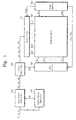
- FIG. 1 is a schematic block diagram illustrating a display device according to an embodiment of the inventive concept
- FIG. 2 is a schematic block diagram illustrating a display panel included in a display device according to an embodiment of the inventive concept
- FIG. 3 is a circuit diagram illustrating a pixel included in a display panel of a display device according to an embodiment of the inventive concept
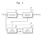
- FIG. 4 is a schematic block diagram illustrating a gray scale converter and a scale factor generator which are included in a display device according to an embodiment of the inventive concept;
- FIG. 5 is a flowchart illustrating an operation of a scale factor generator which is included in a display device according to an embodiment of the inventive concept
- FIG. 6 is a diagram showing a simulation result of a display device according to an embodiment of the inventive concept.
- FIG. 7 is a diagram showing a simulation result of a display device according to an embodiment of the inventive concept.
- inventive concept will be described below in more detail, with reference to the accompanying drawings.
- inventive concept may, however, be embodied in different forms, and should not be construed as limited to the embodiments set forth herein. Rather, these embodiments are provided so that this disclosure will be thorough, and will fully convey the scope of the inventive concept to those skilled in the art.
- Embodiments described and exemplified herein include any and all complementary embodiments.
- the term “and/or” is used to mean the inclusion of at least one of preceding or succeeding elements.
- like reference numerals refer to like elements throughout.
- FIG. 1 is a schematic block diagram illustrating a display device according to an embodiment of the inventive concept.
- FIG. 2 is a schematic block diagram illustrating a display panel included in a display device according to an embodiment of the inventive concept.
- FIG. 3 is a circuit diagram illustrating a pixel included in a display panel of a display device according to an embodiment of the inventive concept. For conciseness, a pixel connected to an nth gate line GLn and an mth data line DLm is illustrated.
- a display device includes a display panel 100, a scan driver 110, a data driver 120, a power source 130, a timing controller 140, a gray scale converter 150, and a scale factor generator 160.
- the display panel 100 includes a plurality of gate lines GL1 to GLn extending in a first direction, a plurality of data lines DL1 to DLm extending in a second direction substantially perpendicular to the first direction and crossing the plurality of gate lines GL1 to GLn, and a plurality of pixel cells P.
- Each of the pixel cells P is connected to one gate line and one data line.
- Pixel cells P aligned in the first direction form a row
- pixel cells P aligned in the second direction form a column.
- Pixel cells P included in the same row are connected to a same gate line
- pixel cells P included in the same column are connected to a same data line.
- the gate lines GL1 to GLn extend between adjacent rows of pixels P
- the data lines DL1 to DLm extend between adjacent columns of pixels P.
- the gate lines GL1 to GLn may apply a gate voltage Gv supplied from the scan driver 110 to the pixel cells P.
- the data lines DL1 to DLm may apply a data output voltage Dv supplied from the data driver 120 to the pixel cells P.
- each of the pixel cells P may include a switching device, a storage device, and/or a light emitting device.
- Each switching device includes a switching transistor Ts and a driving transistor Td.
- the storage device is a capacitor C
- the light emitting device is an organic light emitting diode (OLED).
- Each OLED may includes an anode electrode, a cathode electrode, and an organic emission layer between the anode electrode and the cathode electrode.
- Each organic emission layer includes a hole injection layer (HIL), a hole transport layer (HTL), an emission layer (EML), an electron transport layer (ETL), and/or an electron injection layer (EIL).
- the hole injection layer may be adjacent to the anode electrode, and the electron injection layer may be adjacent to the cathode electrode. Holes supplied through the hole injection layer and the hole transport layer recombine with electrons supplied through the electron injection layer and the electron transport layer in the emission layer, and the OLED may correspondingly emit light.
- the switching transistor Ts is connected between the data line DLm and a first node N1.
- the switching transistor Ts may be turned on by the gate voltage Gv applied through the gate line GLn and transfer the data output voltage Dv applied through the data line DLm to the first node N1.
- the data output voltage Dv transferred to the first node N1 may be stored in the storage capacitor C connected between the first node N1 and a second node N2.
- the driving transistor Td may be turned on by the data output voltage Dv transferred to the first node N1, When the driving transistor Td is turned on, a driving current I may be applied to an OLED via a voltage difference between a first power source voltage VDD and a second power source voltage VSS.
- the first power source voltage VDD may be applied to the anode of the OLED
- the second power source voltage VSS may be applied to the cathode of the OLED.
- An intensity or magnitude of the driving current I may be determined by the data output voltage Dv applied to the driving transistor Td.
- a brightness (e.g., a gray level representation) of the OLED may be proportional to the intensity of the driving current I. Accordingly, the brightness of the OLED may be determined by the data output voltage Dv.
- the scan driver 110 may receive a gate-on voltage Von and a gate-off voltage Voff from the power source 130, receive a gate control signal GCS from the timing controller 140, select any one of the gate lines GL1 to GLn and apply a gate voltage to the selected gate line.
- the scan driver 110 may control the timing of the gate voltage supplied to the gate lines GL1 to GLn in response to the gate control signal GCS.
- the scan driver 110 may sequentially apply the gate voltage from the first gate line GL1 to the nth gate line GLn (e.g., in the second direction).
- a switching transistor which is included in a pixel cell connected to the selected gate line receiving the gate voltage, may be turned on, and switching transistors, which are respectively included in pixel cells connected to unselected gate lines not receiving the gate voltage, may be turned off.
- the scan driver 110 may be directly formed on a substrate where the display panel 100 is formed.
- the data driver 120 may receive an analog driving voltage AVDD from the power source 130 and receive the gray scale-converted pixel data signals R1, G1 and B1 of an n-th frame and a data voltage control signal DCS from the timing controller 140.
- the data driver 120 may convert the gray scale-converted pixel data signals R1, G1 and B1 into analog voltages, and respectively supply data output voltages (e.g., the analog voltages) to the data lines DL1 to DLm.
- the gray scale-converted pixel data signals R1, G1 and B1 may be converted into data output voltages applied to pixel cells that include a red OLED, a green OLED and a blue OLED, respectively.
- the power source 130 may supply a gate-on voltage Von and a gate-off voltage Voff to the scan driver 110.
- the power source 130 may supply the analog driving voltage AVDD to the data driver 120.
- the power source 130 may supply the first power source voltage VDD and the second power source voltage VSS that are applied to the OLEDs of the pixel cells P of the display panel 100.
- the timing controller 140 may receive the gray scale-converted pixel data signals R1, G1 and B1 of an nth frame from the gray scale converter 150.
- the timing controller 140 may transmit the gray scale-converted pixel data signals R1, G1 and B1 and the data voltage control signal DCS to the data driver 120, and transmit the gate control signal GCS to the scan driver 110.
- the gray scale converter 150 may receive pixel data signals R, G and B of an n-th frame from the outside and receive a scale factor S n of the n-th frame from the scale factor generator 160.
- the gray scale converter 150 may multiply the pixel data signals R, G and B by the scale factor S n to change the gray scale information of a frame to be displayed. Therefore, an overcurrent can be prevented or reduced from flowing in the OLEDs of the display panel 100.
- the scale factor generator 160 may receive the pixel data signals R, G and B of the n-th frame and generate the scale factor S n of the n-th frame.
- the scale factor S n may be transmitted to the gray scale converter 150.
- the gray scale converter 150 and the scale factor generator 160 will be described below in detail with reference to FIGS. 4 and 5 .
- FIG. 4 is a schematic block diagram illustrating a gray scale converter and a scale factor generator which are included in a display device according to an embodiment of the inventive concept, such as the one described above.
- FIG. 5 is a flowchart illustrating an operation of a scale factor generator which is included in a display device according to an embodiment of the inventive concept.
- the gray scale converter 150 includes a frame memory 152 and a pixel data converter 154.
- the frame memory 152 may store the pixel data signals R, G and B of an n-th frame while the scale factor S n of the n-th frame is being generated.
- the pixel data converter 154 may receive the pixel data signals R, G and B of the n-th frame from the frame memory 152, receive the scale factor S n of the n-th frame from the scale factor generator 160, and calculate the gray scale-converted pixel data signals R1, G1 and B1.
- the gray scale-converted pixel data signals R1, G1 and B1 may have a gray scale-converted value that is obtained, for example, by multiplying the pixel data signals R, G and B of the n-th frame by the scale factor S n of the n-th frame.
- the scale factor generator 160 includes a data calculator 162 and a data comparator 164.
- the data calculator 162 may receive the pixel data signals R, G and B of the n-th frame and calculate data for calculating the scale factor S n of the n-th frame.
- the data calculator 162 may receive a scale factor determination signal Sdi to calculate the scale factor S n , and transmit the scale factor S n to the pixel data converter 154.
- the data comparator 164 may compare preset values and data received from the data calculator 162 to generate the scale factor determination signal Sdi, and transmit the generated signal to the data calculator 162.
- the scale factor generator 160 may generate the scale factor S n to maintain a current value consumed in the display panel 100 to be below a certain value.
- the data calculator 162 may calculate an original current value I and a conversion current value l c projected or estimated to be consumed in or to be transmitted through the pixel cells P of the display panel 100.
- the original current value I may be calculated with the pixel data signals R, G and B of the n-th frame transferred to the data calculator 162.
- the original current value I may be calculated as expressed in Equation (1) below. I ⁇ E R ⁇ a R ⁇ + E G ⁇ b G ⁇ + E B ⁇ c B ⁇ where a gamma value ( ⁇ ) is a constant from 1.8 to 2.6 that is changed according to the display panel 100.
- E R , E G and E B are efficiency coefficients that are changed with the kinds of materials included in a red OLED, a green OLED and a blue OLED, respectively.
- E R may be 1
- E G may be 2
- E B may be 4.
- a value of R ⁇ may be added by or correspond to a number "a" of pixel cells including a red OLED.
- a value of G ⁇ may be added by or correspond to a number "b" of pixel cells including a green OLED.
- a value of BY may be added by or correspond to a number "c" of pixel cells including a blue OLED.
- the data calculator 162 may also calculate the conversion current value l c .
- the conversion current value l c may be, for example, a current value projected or estimated to be consumed by the display panel 100 in the n-th frame when the pixel data signals R, G and B of the n-th frame are converted with or adjusted by a scale factor S n-1 of an n-1-th frame.
- the conversion current value l c may be a gray scale-converted value that is obtained by multiplying the pixel data signals R, G and B of the n-th frame by the scale factor S n-1 of the n-1-th frame.
- the conversion current value l c may be calculated as expressed in Equation (2) below.
- the data calculator 162 may transfer the conversion current value l c to the data comparator 164.
- the data calculator 162 may calculate a variable factor ( ⁇ ).
- the variable factor ( ⁇ ) may have or represent, for example, a difference between the conversion current value l c and a threshold current value l th .
- the variable factor ( ⁇ ) may be calculated as expressed in Equation (3) below.
- ⁇ I C - I th
- the threshold current value l th may be a preset value as, for example, a value lower than a maximum current consumption value of the display panel 100.
- the threshold current value l th may have or represent, for example, about 20 to 30 % of the maximum current consumption value.
- the threshold current value l th may be set to be about 6 A when the maximum current consumption value of the display panel 100 is about 30 A.
- the data comparator 164 may compare the conversion current value l C received from the data calculator 162 with an overcurrent prevention current value l OP , an upper limit threshold current value l th,U , and/or a lower limit threshold current value [ th , L , to determine and transmit a scale factor determination signal Sdi to the data calculator 162.
- the data comparator 164 may compare the conversion current value l c and an overcurrent prevention current value l OP .
- the overcurrent prevention current value l OP may be a preset value representing an amount of current that the actual current flowing in the display panel 100 should not exceed.
- the overcurrent prevention current value l OP may be set to be a value greater than the threshold current value l th and less than the maximum current consumption value.
- the overcurrent prevention current value l OP may be, for example, about 40 % of the maximum current consumption value.
- the overcurrent prevention current value l OP may be set to be about 12 A when the maximum current consumption value is about 30 A.
- the data comparator 164 compares the conversion current value l c and the overcurrent prevention current value l OP , and when the conversion current value l c is greater than the overcurrent prevention current value l OP , the data comparator 164 may transmit a first scale factor determination signal Sd1 to the data calculator 162. The data calculator 162 may then calculate the scale factor S n of the nth frame in response to or based on the first scale factor determination signal Sd1.
- the data calculator 162 may set the scale factor S n of the nth frame, such that the original current value I projected to be consumed in the display panel 100 is adjusted so as not to exceed the overcurrent prevention current value l OP , in response to the first scale factor determination signal Sd1.
- the scale factor S n may be set to satisfy the condition of Equation (4) below.
- the scale factor S n may have a value that is inversely proportional to the original current value I and proportional to the overcurrent prevention current value l OP .
- the scale factor S n may be transmitted to the pixel data converter 154 and multiplied with the pixel data signals R, G and B of the n-th frame, thereby converting the corresponding gray levels.
- the final (e.g., adjusted) current value l f to be consumed by utilizing the gray scale-converted pixel data signals R1, G1 and B1 of the n-th frame may be calculated as expressed in Equation (6) below.
- I f ⁇ E R ⁇ a S n ⁇ R ⁇ + E G ⁇ b S n ⁇ G ⁇ + E B ⁇ c S n ⁇ B ⁇ S n ⁇ ⁇ I
- the scale factor S n of the n-th frame may then be set in order for the final current value l f consumed in the n-th frame to stay below and not to exceed the overcurrent prevention current value l OP .
- a current value to be consumed by the display panel 100 in the n-th frame should not exceed the overcurrent prevention current value l OP , and thus an overcurrent flowing in the display panel 100 can be minimized or reduced. Therefore, overcurrents being supplied to the OLEDs of the display panel 100 are minimized or reduced, and accordingly, a display device can be provided which has high reliability, is optimized for low power consumption, and has an increased service life.
- the data comparator 164 may compare whether the conversion current value l c is within a range from a lower limit threshold current value l th,L to an upper limit threshold current value l th,U .
- the lower limit threshold current value l th,L may be a value that is preset to be lower than the threshold current value l th
- the upper limit threshold current value l th,U may be a value that is preset to be higher than the threshold current value l th .
- the lower limit threshold current value l th , L may be less than the threshold current value l th by about 1 % of the threshold current value l th
- the upper limit threshold current value l th,U may be greater than the threshold current value l th by about 1 % of the threshold current value I th .
- the data comparator 164 may transmit a second scale factor determination signal Sd2 to the data calculator 162.
- the data calculator 162 may then calculate the scale factor S n in response to or based on the second scale factor determination signal Sd2.
- the data calculator 162 may set the scale factor S n of the n-th frame to be equal to or the same as the scale factor S n-1 of the n-1-th frame, in response to the second scale factor determination signal Sd2. Accordingly, the conversion current value l c may substantially correspond to a total current value to be used in the display panel 100.
- the scale factor S n may be fixed or remain the same. Therefore, an amount of current flowing in the display panel 100 may be prevented from having fine fluctuations, or occurrences of the same may be reduced, and thus a display device having high reliability and more stability can be provided.
- the scale factor S n may also finely fluctuate. That is, even when a fine or small difference between the conversion current value l C and the threshold current value l th occurs due to noise or the like, the scale factor S n may consequently fluctuate in each frame as well. Therefore, a current value flowing in the display panel 100 may also constantly fluctuate, and operation of the display panel 100 may be unstable.
- the scale factor S n may be fixed or remain constant, and thus a display device having high reliability and more stability can be provided.
- the data comparator 164 may transmit a third scale factor determination signal Sd3 to the data calculator 162.
- the data calculator 162 may then calculate the scale factor S n of the n-th frame in response to or based on the third scale factor determination signal Sd3.
- the data calculator 162 may calculate the scale factor S n of the n-th frame as expressed in Equation (7) below, in response to the third scale factor determination signal Sd3.
- S n S n - 1 - a ⁇ ⁇ N
- "a” may be a preset positive constant having an absolute value equal to or less than 1
- "N” may be a preset constant between, for example, 32 to 1024.
- the constants "a” and “N” may be set in order for the scale factor to have a value between 0 and 1.
- N When "N” has too low a value, the amount of change or variation in the scale factor S n may be large, and therefore, a difference of current values consumed by the display panel 100 in each frame may also be large, thereby degrading the reliability of performance of the display device.
- “N” when "N” has too high a value, the amount of change or variation in the scale factor S n may be too small, and therefore, it may be more difficult to control or adjust current values consumed by the display panel 100 because an adjustment amount of current values consumed by the display panel 100 in each frame may not be adjusted significantly. Therefore, "N” may be set on the basis of the above-described considerations. For example, in one embodiment, "N" may be set to be 256.
- the variable factor ( ⁇ ) When the conversion current value I C is less than the lower limit threshold current value l th,L , the variable factor ( ⁇ ) may be calculated as a negative value. Accordingly, the scale factor S n of the n-th frame may be increased to be greater than the scale factor S n-1 of the n-1-th frame. On the other hand, when the conversion current value l c is greater than the upper limit threshold current value l th,U , the variable factor ( ⁇ ) may be calculated as a positive value. Therefore, the scale factor S n of the n-th frame may be decreased to be less than the scale factor S n-1 of the n-1-th frame.
- the scale factor S n of the n-th frame may then be transferred to the pixel data converter 154 and be multiplied by the pixel data signals R, G and B of the n-th frame.
- FIG. 6 is a diagram showing a simulation result of a display device according to an embodiment of the inventive concept.
- the X axis indicates number of frames, and the Y axis indicates current consumption.
- a maximum current consumption value is 100 (e.g., 100% consumption).
- a line (a) of FIG. 6 shows a measured result of current consumption values of a display panel of a display device including a scale factor generator according to an embodiment of the inventive concept, and it is assumed that in the embodiment, an overcurrent prevention current value l op is set to be about 40 % of the maximum current consumption value and the threshold current value l th is set to be about 25 % of the maximum current consumption value.
- a line (b) of FIG. 6 shows a measured result of current consumption values of a display panel of a display device when the operation of FIG.
- a current value consumed in the display panel may temporarily or briefly be higher than the threshold current value l th , but it should not exceed the overcurrent prevention current value l op .
- frames exist where an overcurrent flowing in the display panel not only exceeds the threshold current value l th , but also greatly exceeds the overcurrent prevention current value l op . According to an embodiment of the inventive concept, therefore, an overcurrent exceeding the overcurrent prevention current value l op is prevented or reduced from flowing to the display panel, and thus the reliability and service life of the display panel can increase or improve.
- FIG. 7 is a diagram showing a simulation result of a display device according to an embodiment of the inventive concept.
- the X axis indicates time "s"
- the Y axis indicates power consumption of the display panel.
- Lines (c) and (d) of FIG. 7 show measured results of power consumption based on time in a display device including a scale factor generator according to embodiments of the inventive concept.
- an overcurrent prevention current value l op was set to about 40 % of the maximum current value
- a threshold current value l th was set to about 25 % of the maximum current value.
- the overcurrent prevention current value l op was set to about 40 % of the maximum current value and the threshold current value l th was set to about 35 % of the maximum current value.
- the line (e) of FIG. 7 shows a measured result of power consumption of a display device which does not include a scale factor generator according to an embodiment of the inventive concept.
- the power consumption of a display device including a scale factor generator according to embodiments of the inventive concept is lower than the power consumption of a display device which does not include a scale factor generator.
- the overcurrent prevention current values l op are the same, the power consumption of the display panel may be further controlled based on, for example, variations in the threshold current value l th . Therefore, a display device optimized for low power can be provided.
- a display device includes a scale factor generator that compares a conversion current value and an overcurrent prevention current value to generate a scale factor for an n-th frame, and a gray scale converter that converts a gray scale or gray levels of pixel data signals of the n-th frame by, for example, multiplying them with the scale factor of the n-th frame.
- the scale factor of the n-th frame is set such that total current values to be consumed by the gray scale-converted pixel data of the n-th frame should not exceed the overcurrent prevention current value, and thus a display device having high reliability can be implemented.
Landscapes
- Engineering & Computer Science (AREA)
- Physics & Mathematics (AREA)
- Computer Hardware Design (AREA)
- General Physics & Mathematics (AREA)
- Theoretical Computer Science (AREA)
- Control Of El Displays (AREA)
- Control Of Indicators Other Than Cathode Ray Tubes (AREA)
- Electroluminescent Light Sources (AREA)
Abstract
Description
- The present disclosure relates to a display device and a driving method thereof.
- Recently, lighter and thinner display devices such as monitors and televisions have been developed. As a type of display device that satisfies such characteristics, organic light emitting diode (OLED) displays are attracting much attention.
- OLED displays include two electrodes, and an emission layer disposed therebetween. In OLED displays, an electron injected from one of the two electrodes and a hole injected from the other electrode are combined in the emission layer to form an exciton, and the exciton releases energy to emit light. The electrode includes a thin film transistor for controlling the emission layer.
- Since OLED displays are self-emitting display devices, a current supply line is additionally utilized to drive OLED displays. When an overcurrent is supplied to an OLED display through a current supply line, the service life of the OLED display can be shortened. Therefore, research is being done to prevent or reduce overcurrent from flowing in OLED displays.
- The present invention sets out to provide a display device which increases service life.
- The present invention also sets out to provide a display device which minimizes or reduces the generation of an overcurrent.
- The present invention also seeks to provide a display device having high reliability.
- Embodiments of the inventive concept provide a display device including: a display panel including a plurality of pixels; a gray scale converter for converting gray levels of pixel data signals of a current frame by multiplying the pixel data signals of the current frame by a scale factor of the current frame; and a scale factor generator for comparing a conversion current value with an overcurrent prevention current value to generate the scale factor of the current frame, wherein the conversion current value is a current value projected to be consumed by the display panel utilizing the pixel data signals of the current frame multiplied by a scale factor of a previous frame, and wherein the overcurrent prevention current value is less than a maximum current consumption value of the display panel and greater than a threshold current value of the display panel that is also less than the maximum current consumption value.
- In some embodiments, when the conversion current value is greater than the overcurrent prevention current value, the scale factor of the current frame may be configured to be increased when the overcurrent prevention current value is increased.
- In other embodiments, the scale factor of the current frame may be configured to be decreased when an original current value projected to be consumed by the display panel when a scale factor is not applied is increased.
- In still other embodiments, the scale factor of the current frame may be set to be a value obtained by dividing the overcurrent prevention current value by the original current value, and then raising the result to the 1/γ-th power, wherein γ corresponds to a gamma value of the display panel.
- In even other embodiments, when the conversion current value is less than the overcurrent prevention current value, the scale factor generator may be configured to compare the conversion current value with a lower limit threshold current value and an upper limit threshold current value to generate the scale factor of the current frame, wherein the lower limit threshold current value is less than the threshold current value, and the upper limit threshold current value is greater than the threshold current value and less than the overcurrent prevention current value.
- In yet other embodiments, a difference between the lower limit threshold current value and the threshold current value and a difference between the upper limit threshold current value and the threshold current value may each be equal to or less than about 1 % of the threshold current value.
- In further embodiments, when the conversion current value has a value between the lower limit threshold current value and the upper limit threshold current value, the scale factor of the current frame may be set to be the same as the scale factor of the previous frame.
- In still further embodiments, when the conversion current value is outside of a range from the lower limit threshold current value to the upper limit threshold current value, the scale factor of the current frame may be adjusted from the scale factor of the previous frame by an amount proportional to a value obtained by subtracting the threshold current value from the conversion current value.
- In even further embodiments, when the conversion current value is less than the lower limit threshold current value, the scale factor of the current frame may be adjusted to be greater than the scale factor of the previous frame.
- In yet further embodiments, when the conversion current value is greater than the upper limit threshold current value, the scale factor of the current frame may be adjusted to be less than the scale factor of the previous frame.
- In more embodiments, the scale factor of the current frame and the scale factor of the previous frame may each be greater than 0 and equal to or less than 1.
- In still more embodiments, the gray scale converter may include: a frame memory for storing the pixel data signals of the current frame; and a pixel data converter for converting the gray levels of the pixel data signals of the current frame.
- In even more embodiments, the frame memory may be configured to transmit the pixel data signals of the current frame to the pixel data converter, and the pixel data converter may be configured to multiply the pixel data signal of the current frame by the scale factor of the current frame.
- In other embodiments of the inventive concept, a driving method for a display device includes: multiplying pixel data signals of a current frame by a scale factor of a previous frame to calculate a conversion current value projected to be consumed by a display panel; comparing the conversion current value with an overcurrent prevention current value; generating a scale factor of the current frame; and converting gray levels of the pixel data signals of the current frame by multiplying the pixel data signals of the current frame by the scale factor of the current frame, wherein the overcurrent prevention current value is less than a maximum current consumption value of the display panel and greater than a threshold current value of the display panel that is also less than the maximum current consumption value.
- In some embodiments, the driving method may further include calculating an original current value projected to be consumed by the display panel utilizing the pixel data signals of the current frame when a scale factor is not applied.
- In other embodiments, when the conversion current value is greater than the overcurrent prevention current value, the scale factor of the current frame may be set such that a current value to be consumed by the display panel utilizing the pixel data signals of the current frame multiplied by the scale factor of the current frame is less than the overcurrent prevention current value.
- In still other embodiments, when the conversion current value is less than the overcurrent prevention current value, the driving method may further include determining whether the conversion current value is within a range of the threshold current value.
- In even other embodiments, when the conversion current value is within the range of the threshold current value, the scale factor of the current frame may be set to be the same as the scale factor of the previous frame.
- In yet other embodiments, the driving method may further include calculating a value obtained by subtracting the threshold current value from the conversion current value.
- In further embodiments, when the conversion current value is outside of the range of the threshold current value, the scale factor of the current frame may be adjusted from the scale factor of the previous frame by an amount corresponding to the value obtained by subtracting the threshold current value from the conversion current value.
- At least some of the above and other features of the invention are set out in the claims.
- The accompanying drawings are included to provide a further understanding of the inventive concept. The drawings illustrate exemplary embodiments of the inventive concept and, together with the description, serve to explain principles of the inventive concept. In the drawings:
-
FIG. 1 is a schematic block diagram illustrating a display device according to an embodiment of the inventive concept; -
FIG. 2 is a schematic block diagram illustrating a display panel included in a display device according to an embodiment of the inventive concept; -
FIG. 3 is a circuit diagram illustrating a pixel included in a display panel of a display device according to an embodiment of the inventive concept; -
FIG. 4 is a schematic block diagram illustrating a gray scale converter and a scale factor generator which are included in a display device according to an embodiment of the inventive concept; -
FIG. 5 is a flowchart illustrating an operation of a scale factor generator which is included in a display device according to an embodiment of the inventive concept; -
FIG. 6 is a diagram showing a simulation result of a display device according to an embodiment of the inventive concept; and -
FIG. 7 is a diagram showing a simulation result of a display device according to an embodiment of the inventive concept. - Embodiments of the inventive concept will be described below in more detail, with reference to the accompanying drawings. The inventive concept may, however, be embodied in different forms, and should not be construed as limited to the embodiments set forth herein. Rather, these embodiments are provided so that this disclosure will be thorough, and will fully convey the scope of the inventive concept to those skilled in the art.
- Embodiments described and exemplified herein include any and all complementary embodiments. In the specification, the term "and/or" is used to mean the inclusion of at least one of preceding or succeeding elements. In addition, like reference numerals refer to like elements throughout.
-
FIG. 1 is a schematic block diagram illustrating a display device according to an embodiment of the inventive concept.FIG. 2 is a schematic block diagram illustrating a display panel included in a display device according to an embodiment of the inventive concept.FIG. 3 is a circuit diagram illustrating a pixel included in a display panel of a display device according to an embodiment of the inventive concept. For conciseness, a pixel connected to an nth gate line GLn and an mth data line DLm is illustrated. - Referring to
FIG. 1 , a display device according to an embodiment of the inventive concept includes adisplay panel 100, ascan driver 110, adata driver 120, apower source 130, atiming controller 140, agray scale converter 150, and ascale factor generator 160. - Referring to
FIG. 2 , thedisplay panel 100 includes a plurality of gate lines GL1 to GLn extending in a first direction, a plurality of data lines DL1 to DLm extending in a second direction substantially perpendicular to the first direction and crossing the plurality of gate lines GL1 to GLn, and a plurality of pixel cells P. Each of the pixel cells P is connected to one gate line and one data line. Pixel cells P aligned in the first direction form a row, and pixel cells P aligned in the second direction form a column. Pixel cells P included in the same row are connected to a same gate line, and pixel cells P included in the same column are connected to a same data line. The gate lines GL1 to GLn extend between adjacent rows of pixels P, and the data lines DL1 to DLm extend between adjacent columns of pixels P. - The gate lines GL1 to GLn may apply a gate voltage Gv supplied from the
scan driver 110 to the pixel cells P. The data lines DL1 to DLm may apply a data output voltage Dv supplied from thedata driver 120 to the pixel cells P. - Referring to
FIG. 3 , each of the pixel cells P may include a switching device, a storage device, and/or a light emitting device. Each switching device includes a switching transistor Ts and a driving transistor Td. The storage device is a capacitor C, and the light emitting device is an organic light emitting diode (OLED). - Each OLED may includes an anode electrode, a cathode electrode, and an organic emission layer between the anode electrode and the cathode electrode. Each organic emission layer includes a hole injection layer (HIL), a hole transport layer (HTL), an emission layer (EML), an electron transport layer (ETL), and/or an electron injection layer (EIL). The hole injection layer may be adjacent to the anode electrode, and the electron injection layer may be adjacent to the cathode electrode. Holes supplied through the hole injection layer and the hole transport layer recombine with electrons supplied through the electron injection layer and the electron transport layer in the emission layer, and the OLED may correspondingly emit light.
- In each case the switching transistor Ts is connected between the data line DLm and a first node N1. The switching transistor Ts may be turned on by the gate voltage Gv applied through the gate line GLn and transfer the data output voltage Dv applied through the data line DLm to the first node N1. The data output voltage Dv transferred to the first node N1 may be stored in the storage capacitor C connected between the first node N1 and a second node N2.
- The driving transistor Td may be turned on by the data output voltage Dv transferred to the first node N1, When the driving transistor Td is turned on, a driving current I may be applied to an OLED via a voltage difference between a first power source voltage VDD and a second power source voltage VSS. The first power source voltage VDD may be applied to the anode of the OLED, and the second power source voltage VSS may be applied to the cathode of the OLED.
- An intensity or magnitude of the driving current I may be determined by the data output voltage Dv applied to the driving transistor Td. A brightness (e.g., a gray level representation) of the OLED may be proportional to the intensity of the driving current I. Accordingly, the brightness of the OLED may be determined by the data output voltage Dv.
- Referring again to
FIGS. 1 and2 , thescan driver 110 may receive a gate-on voltage Von and a gate-off voltage Voff from thepower source 130, receive a gate control signal GCS from thetiming controller 140, select any one of the gate lines GL1 to GLn and apply a gate voltage to the selected gate line. Thescan driver 110 may control the timing of the gate voltage supplied to the gate lines GL1 to GLn in response to the gate control signal GCS. - For example, the
scan driver 110 may sequentially apply the gate voltage from the first gate line GL1 to the nth gate line GLn (e.g., in the second direction). A switching transistor, which is included in a pixel cell connected to the selected gate line receiving the gate voltage, may be turned on, and switching transistors, which are respectively included in pixel cells connected to unselected gate lines not receiving the gate voltage, may be turned off. Thescan driver 110 may be directly formed on a substrate where thedisplay panel 100 is formed. - The
data driver 120 may receive an analog driving voltage AVDD from thepower source 130 and receive the gray scale-converted pixel data signals R1, G1 and B1 of an n-th frame and a data voltage control signal DCS from thetiming controller 140. Thedata driver 120 may convert the gray scale-converted pixel data signals R1, G1 and B1 into analog voltages, and respectively supply data output voltages (e.g., the analog voltages) to the data lines DL1 to DLm. The gray scale-converted pixel data signals R1, G1 and B1 may be converted into data output voltages applied to pixel cells that include a red OLED, a green OLED and a blue OLED, respectively. - The
power source 130 may supply a gate-on voltage Von and a gate-off voltage Voff to thescan driver 110. Thepower source 130 may supply the analog driving voltage AVDD to thedata driver 120. Thepower source 130 may supply the first power source voltage VDD and the second power source voltage VSS that are applied to the OLEDs of the pixel cells P of thedisplay panel 100. - The
timing controller 140 may receive the gray scale-converted pixel data signals R1, G1 and B1 of an nth frame from thegray scale converter 150. Thetiming controller 140 may transmit the gray scale-converted pixel data signals R1, G1 and B1 and the data voltage control signal DCS to thedata driver 120, and transmit the gate control signal GCS to thescan driver 110. - The
gray scale converter 150 may receive pixel data signals R, G and B of an n-th frame from the outside and receive a scale factor Sn of the n-th frame from thescale factor generator 160. Thegray scale converter 150 may multiply the pixel data signals R, G and B by the scale factor Sn to change the gray scale information of a frame to be displayed. Therefore, an overcurrent can be prevented or reduced from flowing in the OLEDs of thedisplay panel 100. - The
scale factor generator 160 may receive the pixel data signals R, G and B of the n-th frame and generate the scale factor Sn of the n-th frame. The scale factor Sn may be transmitted to thegray scale converter 150. Thegray scale converter 150 and thescale factor generator 160 will be described below in detail with reference toFIGS. 4 and5 . -
FIG. 4 is a schematic block diagram illustrating a gray scale converter and a scale factor generator which are included in a display device according to an embodiment of the inventive concept, such as the one described above.FIG. 5 is a flowchart illustrating an operation of a scale factor generator which is included in a display device according to an embodiment of the inventive concept. - The
gray scale converter 150 includes aframe memory 152 and apixel data converter 154. Theframe memory 152 may store the pixel data signals R, G and B of an n-th frame while the scale factor Sn of the n-th frame is being generated. Thepixel data converter 154 may receive the pixel data signals R, G and B of the n-th frame from theframe memory 152, receive the scale factor Sn of the n-th frame from thescale factor generator 160, and calculate the gray scale-converted pixel data signals R1, G1 and B1. The gray scale-converted pixel data signals R1, G1 and B1 may have a gray scale-converted value that is obtained, for example, by multiplying the pixel data signals R, G and B of the n-th frame by the scale factor Sn of the n-th frame. - The
scale factor generator 160 includes adata calculator 162 and adata comparator 164. Thedata calculator 162 may receive the pixel data signals R, G and B of the n-th frame and calculate data for calculating the scale factor Sn of the n-th frame. Thedata calculator 162 may receive a scale factor determination signal Sdi to calculate the scale factor Sn, and transmit the scale factor Sn to thepixel data converter 154. Thedata comparator 164 may compare preset values and data received from thedata calculator 162 to generate the scale factor determination signal Sdi, and transmit the generated signal to thedata calculator 162. Thescale factor generator 160 may generate the scale factor Sn to maintain a current value consumed in thedisplay panel 100 to be below a certain value. - Referring now to
FIG. 5 , in operation S10, thedata calculator 162 may calculate an original current value I and a conversion current value lc projected or estimated to be consumed in or to be transmitted through the pixel cells P of thedisplay panel 100. The original current value I may be calculated with the pixel data signals R, G and B of the n-th frame transferred to thedata calculator 162. The original current value I may be calculated as expressed in Equation (1) below.
display panel 100. ER, EG and EB are efficiency coefficients that are changed with the kinds of materials included in a red OLED, a green OLED and a blue OLED, respectively. For example, ER may be 1, EG may be 2, and EB may be 4. A value of Rγ may be added by or correspond to a number "a" of pixel cells including a red OLED. A value of Gγ may be added by or correspond to a number "b" of pixel cells including a green OLED. A value of BY may be added by or correspond to a number "c" of pixel cells including a blue OLED. - The
data calculator 162 may also calculate the conversion current value lc. The conversion current value lc may be, for example, a current value projected or estimated to be consumed by thedisplay panel 100 in the n-th frame when the pixel data signals R, G and B of the n-th frame are converted with or adjusted by a scale factor Sn-1 of an n-1-th frame. The conversion current value lc may be a gray scale-converted value that is obtained by multiplying the pixel data signals R, G and B of the n-th frame by the scale factor Sn-1 of the n-1-th frame. The conversion current value lc may be calculated as expressed in Equation (2) below.
- The
data calculator 162 may transfer the conversion current value lc to thedata comparator 164. - In operation S20, after the conversion current value lc is calculated, the
data calculator 162 may calculate a variable factor (Δ). The variable factor (Δ) may have or represent, for example, a difference between the conversion current value lc and a threshold current value lth. For example, the variable factor (Δ) may be calculated as expressed in Equation (3) below.
display panel 100. The threshold current value lth may have or represent, for example, about 20 to 30 % of the maximum current consumption value. For example, the threshold current value lth may be set to be about 6 A when the maximum current consumption value of thedisplay panel 100 is about 30 A. - The
data comparator 164 may compare the conversion current value lC received from thedata calculator 162 with an overcurrent prevention current value lOP, an upper limit threshold current value lth,U, and/or a lower limit threshold current value [th,L, to determine and transmit a scale factor determination signal Sdi to thedata calculator 162. - In operation S30, The
data comparator 164 may compare the conversion current value lc and an overcurrent prevention current value lOP. The overcurrent prevention current value lOP may be a preset value representing an amount of current that the actual current flowing in thedisplay panel 100 should not exceed. The overcurrent prevention current value lOP may be set to be a value greater than the threshold current value lth and less than the maximum current consumption value. The overcurrent prevention current value lOP may be, for example, about 40 % of the maximum current consumption value. For example, the overcurrent prevention current value lOP may be set to be about 12 A when the maximum current consumption value is about 30 A. - The
data comparator 164 compares the conversion current value lc and the overcurrent prevention current value lOP, and when the conversion current value lc is greater than the overcurrent prevention current value lOP, thedata comparator 164 may transmit a first scale factor determination signal Sd1 to thedata calculator 162. Thedata calculator 162 may then calculate the scale factor Sn of the nth frame in response to or based on the first scale factor determination signal Sd1. - In operation S35, the
data calculator 162 may set the scale factor Sn of the nth frame, such that the original current value I projected to be consumed in thedisplay panel 100 is adjusted so as not to exceed the overcurrent prevention current value lOP, in response to the first scale factor determination signal Sd1. For example, the scale factor Sn may be set to satisfy the condition of Equation (4) below.
- The scale factor Sn may have a value that is inversely proportional to the original current value I and proportional to the overcurrent prevention current value lOP. For example, the scale factor Sn may be calculated as expressed in Equation (5) below.

- The scale factor Sn may be transmitted to the
pixel data converter 154 and multiplied with the pixel data signals R, G and B of the n-th frame, thereby converting the corresponding gray levels. The final (e.g., adjusted) current value lf to be consumed by utilizing the gray scale-converted pixel data signals R1, G1 and B1 of the n-th frame may be calculated as expressed in Equation (6) below.
- Referring back to Equation (2), when the conversion current value lc calculated with the scale factor Sn-1 of an n-1-th frame exceeds an overcurrent prevention current value lop, the scale factor Sn of the n-th frame may then be set in order for the final current value lf consumed in the n-th frame to stay below and not to exceed the overcurrent prevention current value lOP.
- Therefore, according to an embodiment of the inventive concept, a current value to be consumed by the
display panel 100 in the n-th frame should not exceed the overcurrent prevention current value lOP, and thus an overcurrent flowing in thedisplay panel 100 can be minimized or reduced. Therefore, overcurrents being supplied to the OLEDs of thedisplay panel 100 are minimized or reduced, and accordingly, a display device can be provided which has high reliability, is optimized for low power consumption, and has an increased service life. - When the conversion current value lC is less than the overcurrent prevention current value lOP, in operation S40, the
data comparator 164 may compare whether the conversion current value lc is within a range from a lower limit threshold current value lth,L to an upper limit threshold current value lth,U. The lower limit threshold current value lth,L may be a value that is preset to be lower than the threshold current value lth, and the upper limit threshold current value lth,U may be a value that is preset to be higher than the threshold current value lth. For example, the lower limit threshold current value lth,L may be less than the threshold current value lth by about 1 % of the threshold current value lth, and the upper limit threshold current value lth,U may be greater than the threshold current value lth by about 1 % of the threshold current value Ith. - When the conversion current value lc is within the range from the lower limit threshold current value lth,L to the upper limit threshold current value lth,U , the
data comparator 164 may transmit a second scale factor determination signal Sd2 to thedata calculator 162. Thedata calculator 162 may then calculate the scale factor Sn in response to or based on the second scale factor determination signal Sd2. - In operation S45, the
data calculator 162 may set the scale factor Sn of the n-th frame to be equal to or the same as the scale factor Sn-1 of the n-1-th frame, in response to the second scale factor determination signal Sd2. Accordingly, the conversion current value lc may substantially correspond to a total current value to be used in thedisplay panel 100. As described above, when there is a fine or small difference between the conversion current value lc and the threshold current value lth, such that the conversion current value lc has a value between the lower limit threshold current value lth,L and the upper limit threshold current value lth,U , the scale factor Sn may be fixed or remain the same. Therefore, an amount of current flowing in thedisplay panel 100 may be prevented from having fine fluctuations, or occurrences of the same may be reduced, and thus a display device having high reliability and more stability can be provided. - That is, although there may be fine differences between the conversion current value lc and the threshold current value lth by, for example, a degree where the conversion current value Ic has a value within the range from the lower limit threshold current value lth,L to the upper limit threshold current value lth,U, if the scale factor Sn is constantly changed, the scale factor Sn may also finely fluctuate. That is, even when a fine or small difference between the conversion current value lC and the threshold current value lth occurs due to noise or the like, the scale factor Sn may consequently fluctuate in each frame as well. Therefore, a current value flowing in the
display panel 100 may also constantly fluctuate, and operation of thedisplay panel 100 may be unstable. - However, according to an embodiment of the inventive concept, as described above, although there may be fine differences between the conversion current value lc and the threshold current value lth, when the conversion current value lc has a value between the lower limit threshold current value lth,L and the upper limit threshold current value lth,U, the scale factor Sn may be fixed or remain constant, and thus a display device having high reliability and more stability can be provided.
- When the conversion current value lc is not within the range from the lower limit threshold current value lth,L to the upper limit threshold current value lth,U, the
data comparator 164 may transmit a third scale factor determination signal Sd3 to thedata calculator 162. Thedata calculator 162 may then calculate the scale factor Sn of the n-th frame in response to or based on the third scale factor determination signal Sd3. - In operation S50, the
data calculator 162 may calculate the scale factor Sn of the n-th frame as expressed in Equation (7) below, in response to the third scale factor determination signal Sd3.
- When "N" has too low a value, the amount of change or variation in the scale factor Sn may be large, and therefore, a difference of current values consumed by the
display panel 100 in each frame may also be large, thereby degrading the reliability of performance of the display device. On the other hand, when "N" has too high a value, the amount of change or variation in the scale factor Sn may be too small, and therefore, it may be more difficult to control or adjust current values consumed by thedisplay panel 100 because an adjustment amount of current values consumed by thedisplay panel 100 in each frame may not be adjusted significantly. Therefore, "N" may be set on the basis of the above-described considerations. For example, in one embodiment, "N" may be set to be 256. - When the conversion current value IC is less than the lower limit threshold current value lth,L, the variable factor (Δ) may be calculated as a negative value. Accordingly, the scale factor Sn of the n-th frame may be increased to be greater than the scale factor Sn-1 of the n-1-th frame. On the other hand, when the conversion current value lc is greater than the upper limit threshold current value lth,U, the variable factor (Δ) may be calculated as a positive value. Therefore, the scale factor Sn of the n-th frame may be decreased to be less than the scale factor Sn-1 of the n-1-th frame.
- After the scale factor Sn of the n-th frame is determined, the scale factor Sn of the n-th frame may then be transferred to the
pixel data converter 154 and be multiplied by the pixel data signals R, G and B of the n-th frame. -
FIG. 6 is a diagram showing a simulation result of a display device according to an embodiment of the inventive concept. - Referring to
FIG. 6 , the X axis indicates number of frames, and the Y axis indicates current consumption. It is assumed inFIG. 6 that a maximum current consumption value is 100 (e.g., 100% consumption). A line (a) ofFIG. 6 shows a measured result of current consumption values of a display panel of a display device including a scale factor generator according to an embodiment of the inventive concept, and it is assumed that in the embodiment, an overcurrent prevention current value lop is set to be about 40 % of the maximum current consumption value and the threshold current value lth is set to be about 25 % of the maximum current consumption value. A line (b) ofFIG. 6 shows a measured result of current consumption values of a display panel of a display device when the operation ofFIG. 5 is omitted (e.g., without a scale factor generator as described in embodiments of the inventive concept). In the line (a) ofFIG. 6 , a current value consumed in the display panel may temporarily or briefly be higher than the threshold current value lth, but it should not exceed the overcurrent prevention current value lop. However, in the line (b) ofFIG. 6 , frames exist where an overcurrent flowing in the display panel not only exceeds the threshold current value lth, but also greatly exceeds the overcurrent prevention current value lop. According to an embodiment of the inventive concept, therefore, an overcurrent exceeding the overcurrent prevention current value lop is prevented or reduced from flowing to the display panel, and thus the reliability and service life of the display panel can increase or improve. -
FIG. 7 is a diagram showing a simulation result of a display device according to an embodiment of the inventive concept. - Referring to
FIG. 7 , the X axis indicates time "s", and the Y axis indicates power consumption of the display panel. Lines (c) and (d) ofFIG. 7 show measured results of power consumption based on time in a display device including a scale factor generator according to embodiments of the inventive concept. For the line (c) ofFIG. 7 , an overcurrent prevention current value lop was set to about 40 % of the maximum current value, and a threshold current value lth was set to about 25 % of the maximum current value. For the line (d) ofFIG. 7 , the overcurrent prevention current value lop was set to about 40 % of the maximum current value and the threshold current value lth was set to about 35 % of the maximum current value. The line (e) ofFIG. 7 shows a measured result of power consumption of a display device which does not include a scale factor generator according to an embodiment of the inventive concept. As can be seen, for example, inFIG. 7 , the power consumption of a display device including a scale factor generator according to embodiments of the inventive concept is lower than the power consumption of a display device which does not include a scale factor generator. Also, when the overcurrent prevention current values lop are the same, the power consumption of the display panel may be further controlled based on, for example, variations in the threshold current value lth. Therefore, a display device optimized for low power can be provided. - A display device according to embodiments of the inventive concept includes a scale factor generator that compares a conversion current value and an overcurrent prevention current value to generate a scale factor for an n-th frame, and a gray scale converter that converts a gray scale or gray levels of pixel data signals of the n-th frame by, for example, multiplying them with the scale factor of the n-th frame. The scale factor of the n-th frame is set such that total current values to be consumed by the gray scale-converted pixel data of the n-th frame should not exceed the overcurrent prevention current value, and thus a display device having high reliability can be implemented.
- The above-disclosed subject matter is to be considered illustrative and not restrictive, and the appended claims are intended to cover any and all modifications, enhancements, and/or other embodiments, which fall within the true spirit and scope of the inventive concept. Thus, the scope of the inventive concept is to be determined based on a broadest permissible interpretation of the following claims and their equivalents, and shall not be restricted or limited by the foregoing detailed description.
Claims (20)
- A display device comprising:a display panel comprising a plurality of pixels;a gray scale converter for converting gray levels of pixel data signals of a current frame by multiplying the pixel data signals of the current frame by a scale factor of the current frame; anda scale factor generator for comparing a conversion current value with an overcurrent prevention current value to generate the scale factor of the current frame,wherein the conversion current value is a current value projected to be consumed by the display panel utilizing the pixel data signals of the current frame multiplied by a scale factor of a previous frame, andwherein the overcurrent prevention current value is less than a maximum current consumption value of the display panel and greater than a threshold current value of the display panel that is also less than the maximum current consumption value.
- A display device according to claim 1, adapted such that when the conversion current value is greater than the overcurrent prevention current value, the scale factor of the current frame is configured to be increased when the overcurrent prevention current value is increased.
- A display device according to claim 2, adapted such that the scale factor of the current frame is configured to be decreased when an original current value projected to be consumed by the display panel when a scale factor is not applied is increased.
- A display device according to claim 3, adapted such that the scale factor of the current frame is set to be a value obtained by dividing the overcurrent prevention current value by the original current value, and then raising the result to the 1/y-th power, wherein γ corresponds to a gamma value of the display panel.
- A display device according to any preceding claim, adapted such that when the conversion current value is less than the overcurrent prevention current value, the scale factor generator is configured to compare the conversion current value with a lower limit threshold current value and an upper limit threshold current value to generate the scale factor of the current frame,
wherein the lower limit threshold current value is less than the threshold current value, and the upper limit threshold current value is greater than the threshold current value and less than the overcurrent prevention current value. - A display device according to claim 5, wherein a difference between the lower limit threshold current value and the threshold current value and a difference between the upper limit threshold current value and the threshold current value are each equal to or less than about 1 % of the threshold current value.
- A display device according to claim 5 or 6, wherein when the conversion current value has a value between the lower limit threshold current value and the upper limit threshold current value, the scale factor of the current frame is set to be the same as the scale factor of the previous frame.
- A display device of claim 5, 6 or 7, wherein when the conversion current value is outside of a range from the lower limit threshold current value to the upper limit threshold current value, the scale factor of the current frame is adjusted from the scale factor of the previous frame by an amount proportional to a value obtained by subtracting the threshold current value from the conversion current value.
- A display device according to claim 8, adapted such that when the conversion current value is less than the lower limit threshold current value, the scale factor of the current frame is adjusted to be greater than the scale factor of the previous frame.
- A display device according to claim 8 or 9, adapted such that when the conversion current value is greater than the upper limit threshold current value, the scale factor of the current frame is adjusted to be less than the scale factor of the previous frame.
- A display device according to any preceding claim, wherein the scale factor of the current frame and the scale factor of the previous frame are each greater than 0 and equal to or less than 1.
- A display device according to any preceding claim, wherein the gray scale converter comprises:a frame memory for storing the pixel data signals of the current frame; anda pixel data converter for converting the gray levels of the pixel data signals of the current frame.
- A display device according to claim 12, wherein:the frame memory is configured to transmit the pixel data signals of the current frame to the pixel data converter, andthe pixel data converter is configured to multiply the pixel data signals of the current frame by the scale factor of the current frame.
- A driving method for a display device, the driving method comprising:multiplying pixel data signals of a current frame by a scale factor of a previous frame to calculate a conversion current value projected to be consumed by a display panel;comparing the conversion current value with an overcurrent prevention current value;generating a scale factor of the current frame; andconverting gray levels of the pixel data signals of the current frame by multiplying the pixel data signals of the current frame by the scale factor of the current frame,wherein the overcurrent prevention current value is less than a maximum current consumption value of the display panel and greater than a threshold current value of the display panel that is also less than the maximum current consumption value.
- A driving method according to claim 14, further comprising calculating an original current value projected to be consumed by the display panel utilizing the pixel data signals of the current frame when a scale factor is not applied.
- A driving method according to claim 15, wherein when the conversion current value is greater than the overcurrent prevention current value, the scale factor of the current frame is set such that a current value to be consumed by the display panel utilizing the pixel data signals of the current frame multiplied by the scale factor of the current frame is less than the overcurrent prevention current value.
- A driving method according to claim 14, 15 or 16, wherein when the conversion current value is less than the overcurrent prevention current value, the driving method further comprises determining whether the conversion current value is within a range of the threshold current value.
- A driving method according to claim 17, wherein when the conversion current value is within the range of the threshold current value, the scale factor of the current frame is set to be the same as the scale factor of the previous frame.
- A driving method according to claim 17 or 18, further comprising calculating a value obtained by subtracting the threshold current value from the conversion current value.
- A driving method according to claim 19, wherein when the conversion current value is outside of the range of the threshold current value, the scale factor of the current frame is adjusted from the scale factor of the previous frame by an amount corresponding to the value obtained by subtracting the threshold current value from the conversion current value.
Applications Claiming Priority (1)
| Application Number | Priority Date | Filing Date | Title |
|---|---|---|---|
| KR1020100080960A KR101712086B1 (en) | 2010-08-20 | 2010-08-20 | Display device and driving method thereof |
Publications (2)
| Publication Number | Publication Date |
|---|---|
| EP2420989A1 true EP2420989A1 (en) | 2012-02-22 |
| EP2420989B1 EP2420989B1 (en) | 2019-09-25 |
Family
ID=44582421
Family Applications (1)
| Application Number | Title | Priority Date | Filing Date |
|---|---|---|---|
| EP11178119.1A Active EP2420989B1 (en) | 2010-08-20 | 2011-08-19 | Display device and driving method thereof |
Country Status (6)
| Country | Link |
|---|---|
| US (1) | US8854399B2 (en) |
| EP (1) | EP2420989B1 (en) |
| JP (1) | JP6067958B2 (en) |
| KR (1) | KR101712086B1 (en) |
| CN (1) | CN102376253B (en) |
| TW (1) | TWI536343B (en) |
Families Citing this family (30)
| Publication number | Priority date | Publication date | Assignee | Title |
|---|---|---|---|---|
| KR101883925B1 (en) | 2011-04-08 | 2018-08-02 | 삼성디스플레이 주식회사 | Organic Light Emitting Display Device and Driving Method Thereof |
| KR101456958B1 (en) * | 2012-10-15 | 2014-10-31 | 엘지디스플레이 주식회사 | Apparatus and method for driving of organic light emitting display device |
| US9818373B2 (en) * | 2012-10-31 | 2017-11-14 | Sharp Kabushiki Kaisha | Data processing device for display device, display device equipped with same and data processing method for display device |
| KR101970561B1 (en) * | 2012-11-16 | 2019-08-13 | 엘지디스플레이 주식회사 | Organic light emitting diode display device and method for driving the same |
| KR101992895B1 (en) * | 2012-12-10 | 2019-09-27 | 엘지디스플레이 주식회사 | Organic light emitting diode display device and method for driving the same |
| KR102016153B1 (en) * | 2013-05-10 | 2019-08-30 | 삼성디스플레이 주식회사 | Display device, control device for driving the display device, and control method thereof |
| KR102050518B1 (en) | 2013-05-27 | 2019-12-18 | 삼성디스플레이 주식회사 | Power control device and method for a display device |
| KR102047083B1 (en) * | 2013-05-29 | 2019-11-21 | 삼성디스플레이 주식회사 | Display device and control method thereof |
| KR20140141175A (en) * | 2013-05-31 | 2014-12-10 | 삼성디스플레이 주식회사 | Organic light emitting display device and driving method thereof |
| KR102114330B1 (en) * | 2013-10-08 | 2020-05-22 | 엘지디스플레이 주식회사 | Organic light emitting display device |
| KR102105102B1 (en) * | 2013-10-10 | 2020-04-27 | 삼성전자주식회사 | Display device and method thereof |
| KR102199493B1 (en) | 2014-03-17 | 2021-01-07 | 삼성디스플레이 주식회사 | Organic light emitting display device and method for driving the same |
| KR102194666B1 (en) * | 2014-07-02 | 2020-12-24 | 삼성디스플레이 주식회사 | Display panel |
| KR102218642B1 (en) * | 2014-11-27 | 2021-02-23 | 삼성디스플레이 주식회사 | Display device and method of driving a display device |
| KR102453423B1 (en) * | 2015-12-08 | 2022-10-13 | 삼성디스플레이 주식회사 | Method of driving organic light emitting display device and organic light emitting display device performing the same |
| US10297191B2 (en) * | 2016-01-29 | 2019-05-21 | Samsung Display Co., Ltd. | Dynamic net power control for OLED and local dimming LCD displays |
| CN105590587B (en) * | 2016-03-24 | 2017-11-07 | 京东方科技集团股份有限公司 | A kind of gamma correction method and device for display module |
| KR102642615B1 (en) * | 2018-12-07 | 2024-03-05 | 엘지전자 주식회사 | Organic light emitting diode display device |
| EP3664075A1 (en) * | 2018-12-07 | 2020-06-10 | LG Electronics Inc. | Organic light emitting diode display device |
| KR102635405B1 (en) * | 2019-02-26 | 2024-02-14 | 삼성디스플레이 주식회사 | Display device |
| CN112650458B (en) * | 2019-10-10 | 2022-07-08 | 深圳Tcl数字技术有限公司 | Display screen adjusting method, storage medium and terminal equipment |
| CN110767170B (en) * | 2019-11-05 | 2020-11-10 | 深圳市华星光电半导体显示技术有限公司 | Picture display method and picture display device |
| KR102802426B1 (en) * | 2020-09-09 | 2025-05-07 | 삼성디스플레이 주식회사 | Electronic device and driving method of electronic device |
| CN112164360A (en) * | 2020-09-24 | 2021-01-01 | 合肥维信诺科技有限公司 | Display drive circuit and display device |
| KR102872332B1 (en) * | 2021-04-27 | 2025-10-17 | 삼성디스플레이 주식회사 | Display apparatus and method of operating the same |
| KR102827327B1 (en) * | 2021-06-14 | 2025-07-02 | 삼성디스플레이 주식회사 | Display device and method of driving the same |
| KR20230120153A (en) * | 2022-02-07 | 2023-08-17 | 삼성디스플레이 주식회사 | Controller, display device including the same, and method of driving display device using the same |
| KR102949416B1 (en) | 2022-02-14 | 2026-04-09 | 삼성디스플레이 주식회사 | Display device |
| KR102646573B1 (en) | 2022-02-23 | 2024-03-13 | 엘지전자 주식회사 | Display device |
| KR20240010637A (en) * | 2022-07-14 | 2024-01-24 | 삼성디스플레이 주식회사 | Display device and driving method thereof |
Citations (2)
| Publication number | Priority date | Publication date | Assignee | Title |
|---|---|---|---|---|
| US20040201582A1 (en) * | 2003-04-08 | 2004-10-14 | Eastman Kodak Company | Controlling current in display device |
| US20090033602A1 (en) * | 2007-07-30 | 2009-02-05 | Arkhipov Alexander | Organic light-emitting display device and method of driving the same |
Family Cites Families (12)
| Publication number | Priority date | Publication date | Assignee | Title |
|---|---|---|---|---|
| JP2002116732A (en) * | 2000-10-05 | 2002-04-19 | Pioneer Electronic Corp | Luminous panel driving method and device |
| US7071635B2 (en) * | 2001-09-26 | 2006-07-04 | Sanyo Electric Co., Ltd. | Planar display apparatus |
| KR20050032321A (en) * | 2003-10-01 | 2005-04-07 | 삼성에스디아이 주식회사 | Field emission display and deriving me thod thereof |
| JP4111128B2 (en) * | 2003-11-28 | 2008-07-02 | カシオ計算機株式会社 | Display drive device, display device, and drive control method thereof |
| KR100793555B1 (en) * | 2005-04-28 | 2008-01-14 | 삼성에스디아이 주식회사 | Light emitting display |
| KR101157265B1 (en) | 2005-12-30 | 2012-06-15 | 엘지디스플레이 주식회사 | Organic electro luminescence lighting emitting display device |
| JP5248750B2 (en) * | 2006-03-14 | 2013-07-31 | グローバル・オーエルイーディー・テクノロジー・リミテッド・ライアビリティ・カンパニー | Display device driving apparatus and driving method |
| JP4314638B2 (en) * | 2006-08-01 | 2009-08-19 | カシオ計算機株式会社 | Display device and drive control method thereof |
| KR101362981B1 (en) | 2007-01-05 | 2014-02-21 | 삼성디스플레이 주식회사 | Organic light emitting display device and driving method thereof |
| KR100914118B1 (en) * | 2007-04-24 | 2009-08-27 | 삼성모바일디스플레이주식회사 | Organic electroluminescent display and driving method thereof |
| KR100944494B1 (en) | 2008-06-02 | 2010-03-03 | 신코엠 주식회사 | PMLO LED driving circuit and driving method |
| JP4468467B2 (en) * | 2008-06-27 | 2010-05-26 | 株式会社東芝 | Video signal control device, video display system, and video signal control method |
-
2010
- 2010-08-20 KR KR1020100080960A patent/KR101712086B1/en not_active Expired - Fee Related
-
2011
- 2011-02-28 JP JP2011042230A patent/JP6067958B2/en active Active
- 2011-02-28 US US13/037,209 patent/US8854399B2/en active Active
- 2011-08-18 TW TW100129477A patent/TWI536343B/en active
- 2011-08-19 EP EP11178119.1A patent/EP2420989B1/en active Active
- 2011-08-22 CN CN201110244326.5A patent/CN102376253B/en active Active
Patent Citations (2)
| Publication number | Priority date | Publication date | Assignee | Title |
|---|---|---|---|---|
| US20040201582A1 (en) * | 2003-04-08 | 2004-10-14 | Eastman Kodak Company | Controlling current in display device |
| US20090033602A1 (en) * | 2007-07-30 | 2009-02-05 | Arkhipov Alexander | Organic light-emitting display device and method of driving the same |
Also Published As
| Publication number | Publication date |
|---|---|
| KR101712086B1 (en) | 2017-03-14 |
| US20120044270A1 (en) | 2012-02-23 |
| TWI536343B (en) | 2016-06-01 |
| CN102376253A (en) | 2012-03-14 |
| JP6067958B2 (en) | 2017-01-25 |
| US8854399B2 (en) | 2014-10-07 |
| JP2012042914A (en) | 2012-03-01 |
| KR20120017968A (en) | 2012-02-29 |
| CN102376253B (en) | 2015-08-19 |
| TW201225049A (en) | 2012-06-16 |
| EP2420989B1 (en) | 2019-09-25 |
Similar Documents
| Publication | Publication Date | Title |
|---|---|---|
| EP2420989B1 (en) | Display device and driving method thereof | |
| KR102593537B1 (en) | Driving controller, display device having the same and driving method of display device | |
| KR101279117B1 (en) | OLED display and drive method thereof | |
| US8933922B2 (en) | DC-DC converter and organic light emitting display including the same | |
| KR102367483B1 (en) | Organic light emitting diode display devece | |
| US20050269960A1 (en) | Display with current controlled light-emitting device | |
| US8269702B2 (en) | Organic light emitting display device and method of driving the same | |
| CN108269525B (en) | AMOLED display device and driving method thereof | |
| US10825386B2 (en) | OLED driving compensation circuit and AMOLED display panel | |
| US8289253B2 (en) | Method of driving display device to control over-current, circuit of driving display device using the method and display device having the same | |
| JP7316776B2 (en) | semiconductor equipment | |
| KR20090012381A (en) | OLED display and driving method thereof | |
| US11482164B2 (en) | Display device | |
| KR20100011642A (en) | Organic light emitting diode display device | |
| US9779667B2 (en) | Organic light emitting display device and method for driving the same | |
| KR101310376B1 (en) | Organic Light Emitting Diode Display And Driving Method Thereof | |
| US9280932B2 (en) | Organic light emitting display and method for driving the same | |
| JP5319094B2 (en) | Image display device driving method and image display device | |
| KR20080030903A (en) | Organic light emitting diode display device and driving method thereof | |
| KR20200050007A (en) | Display device and driving method of the display device | |
| KR100834169B1 (en) | EL display device and driving method thereof | |
| KR20120123414A (en) | Display device | |
| KR20110061438A (en) | Driving device and driving method of LED display device | |
| KR20110072543A (en) | OLED-based display device and driving method thereof |
Legal Events
| Date | Code | Title | Description |
|---|---|---|---|
| AK | Designated contracting states |
Kind code of ref document: A1 Designated state(s): AL AT BE BG CH CY CZ DE DK EE ES FI FR GB GR HR HU IE IS IT LI LT LU LV MC MK MT NL NO PL PT RO RS SE SI SK SM TR |
|
| AX | Request for extension of the european patent |
Extension state: BA ME |
|
| PUAI | Public reference made under article 153(3) epc to a published international application that has entered the european phase |
Free format text: ORIGINAL CODE: 0009012 |
|
| 17P | Request for examination filed |
Effective date: 20120730 |
|
| RAP1 | Party data changed (applicant data changed or rights of an application transferred) |
Owner name: SAMSUNG DISPLAY CO., LTD. |
|
| 17Q | First examination report despatched |
Effective date: 20150330 |
|
| RAP1 | Party data changed (applicant data changed or rights of an application transferred) |
Owner name: SAMSUNG DISPLAY CO., LTD. |
|
| STAA | Information on the status of an ep patent application or granted ep patent |
Free format text: STATUS: EXAMINATION IS IN PROGRESS |
|
| GRAP | Despatch of communication of intention to grant a patent |
Free format text: ORIGINAL CODE: EPIDOSNIGR1 |
|
| STAA | Information on the status of an ep patent application or granted ep patent |
Free format text: STATUS: GRANT OF PATENT IS INTENDED |
|
| INTG | Intention to grant announced |
Effective date: 20190307 |
|
| GRAS | Grant fee paid |
Free format text: ORIGINAL CODE: EPIDOSNIGR3 |
|
| GRAA | (expected) grant |
Free format text: ORIGINAL CODE: 0009210 |
|
| STAA | Information on the status of an ep patent application or granted ep patent |
Free format text: STATUS: THE PATENT HAS BEEN GRANTED |
|
| AK | Designated contracting states |
Kind code of ref document: B1 Designated state(s): AL AT BE BG CH CY CZ DE DK EE ES FI FR GB GR HR HU IE IS IT LI LT LU LV MC MK MT NL NO PL PT RO RS SE SI SK SM TR |
|
| REG | Reference to a national code |
Ref country code: GB Ref legal event code: FG4D |
|
| REG | Reference to a national code |
Ref country code: CH Ref legal event code: EP |
|
| REG | Reference to a national code |
Ref country code: DE Ref legal event code: R096 Ref document number: 602011062278 Country of ref document: DE |
|
| REG | Reference to a national code |
Ref country code: AT Ref legal event code: REF Ref document number: 1184604 Country of ref document: AT Kind code of ref document: T Effective date: 20191015 |
|
| REG | Reference to a national code |
Ref country code: IE Ref legal event code: FG4D |
|
| REG | Reference to a national code |
Ref country code: NL Ref legal event code: MP Effective date: 20190925 |
|
| PG25 | Lapsed in a contracting state [announced via postgrant information from national office to epo] |
Ref country code: NO Free format text: LAPSE BECAUSE OF FAILURE TO SUBMIT A TRANSLATION OF THE DESCRIPTION OR TO PAY THE FEE WITHIN THE PRESCRIBED TIME-LIMIT Effective date: 20191225 Ref country code: BG Free format text: LAPSE BECAUSE OF FAILURE TO SUBMIT A TRANSLATION OF THE DESCRIPTION OR TO PAY THE FEE WITHIN THE PRESCRIBED TIME-LIMIT Effective date: 20191225 Ref country code: SE Free format text: LAPSE BECAUSE OF FAILURE TO SUBMIT A TRANSLATION OF THE DESCRIPTION OR TO PAY THE FEE WITHIN THE PRESCRIBED TIME-LIMIT Effective date: 20190925 Ref country code: FI Free format text: LAPSE BECAUSE OF FAILURE TO SUBMIT A TRANSLATION OF THE DESCRIPTION OR TO PAY THE FEE WITHIN THE PRESCRIBED TIME-LIMIT Effective date: 20190925 Ref country code: HR Free format text: LAPSE BECAUSE OF FAILURE TO SUBMIT A TRANSLATION OF THE DESCRIPTION OR TO PAY THE FEE WITHIN THE PRESCRIBED TIME-LIMIT Effective date: 20190925 Ref country code: LT Free format text: LAPSE BECAUSE OF FAILURE TO SUBMIT A TRANSLATION OF THE DESCRIPTION OR TO PAY THE FEE WITHIN THE PRESCRIBED TIME-LIMIT Effective date: 20190925 |
|
| REG | Reference to a national code |
Ref country code: LT Ref legal event code: MG4D |
|
| PG25 | Lapsed in a contracting state [announced via postgrant information from national office to epo] |
Ref country code: GR Free format text: LAPSE BECAUSE OF FAILURE TO SUBMIT A TRANSLATION OF THE DESCRIPTION OR TO PAY THE FEE WITHIN THE PRESCRIBED TIME-LIMIT Effective date: 20191226 Ref country code: RS Free format text: LAPSE BECAUSE OF FAILURE TO SUBMIT A TRANSLATION OF THE DESCRIPTION OR TO PAY THE FEE WITHIN THE PRESCRIBED TIME-LIMIT Effective date: 20190925 Ref country code: LV Free format text: LAPSE BECAUSE OF FAILURE TO SUBMIT A TRANSLATION OF THE DESCRIPTION OR TO PAY THE FEE WITHIN THE PRESCRIBED TIME-LIMIT Effective date: 20190925 |
|
| REG | Reference to a national code |
Ref country code: AT Ref legal event code: MK05 Ref document number: 1184604 Country of ref document: AT Kind code of ref document: T Effective date: 20190925 |
|
| PG25 | Lapsed in a contracting state [announced via postgrant information from national office to epo] |
Ref country code: PT Free format text: LAPSE BECAUSE OF FAILURE TO SUBMIT A TRANSLATION OF THE DESCRIPTION OR TO PAY THE FEE WITHIN THE PRESCRIBED TIME-LIMIT Effective date: 20200127 Ref country code: AL Free format text: LAPSE BECAUSE OF FAILURE TO SUBMIT A TRANSLATION OF THE DESCRIPTION OR TO PAY THE FEE WITHIN THE PRESCRIBED TIME-LIMIT Effective date: 20190925 Ref country code: ES Free format text: LAPSE BECAUSE OF FAILURE TO SUBMIT A TRANSLATION OF THE DESCRIPTION OR TO PAY THE FEE WITHIN THE PRESCRIBED TIME-LIMIT Effective date: 20190925 Ref country code: EE Free format text: LAPSE BECAUSE OF FAILURE TO SUBMIT A TRANSLATION OF THE DESCRIPTION OR TO PAY THE FEE WITHIN THE PRESCRIBED TIME-LIMIT Effective date: 20190925 Ref country code: PL Free format text: LAPSE BECAUSE OF FAILURE TO SUBMIT A TRANSLATION OF THE DESCRIPTION OR TO PAY THE FEE WITHIN THE PRESCRIBED TIME-LIMIT Effective date: 20190925 Ref country code: NL Free format text: LAPSE BECAUSE OF FAILURE TO SUBMIT A TRANSLATION OF THE DESCRIPTION OR TO PAY THE FEE WITHIN THE PRESCRIBED TIME-LIMIT Effective date: 20190925 Ref country code: RO Free format text: LAPSE BECAUSE OF FAILURE TO SUBMIT A TRANSLATION OF THE DESCRIPTION OR TO PAY THE FEE WITHIN THE PRESCRIBED TIME-LIMIT Effective date: 20190925 Ref country code: IT Free format text: LAPSE BECAUSE OF FAILURE TO SUBMIT A TRANSLATION OF THE DESCRIPTION OR TO PAY THE FEE WITHIN THE PRESCRIBED TIME-LIMIT Effective date: 20190925 Ref country code: AT Free format text: LAPSE BECAUSE OF FAILURE TO SUBMIT A TRANSLATION OF THE DESCRIPTION OR TO PAY THE FEE WITHIN THE PRESCRIBED TIME-LIMIT Effective date: 20190925 |
|
| PG25 | Lapsed in a contracting state [announced via postgrant information from national office to epo] |
Ref country code: CZ Free format text: LAPSE BECAUSE OF FAILURE TO SUBMIT A TRANSLATION OF THE DESCRIPTION OR TO PAY THE FEE WITHIN THE PRESCRIBED TIME-LIMIT Effective date: 20190925 Ref country code: SM Free format text: LAPSE BECAUSE OF FAILURE TO SUBMIT A TRANSLATION OF THE DESCRIPTION OR TO PAY THE FEE WITHIN THE PRESCRIBED TIME-LIMIT Effective date: 20190925 Ref country code: IS Free format text: LAPSE BECAUSE OF FAILURE TO SUBMIT A TRANSLATION OF THE DESCRIPTION OR TO PAY THE FEE WITHIN THE PRESCRIBED TIME-LIMIT Effective date: 20200224 Ref country code: SK Free format text: LAPSE BECAUSE OF FAILURE TO SUBMIT A TRANSLATION OF THE DESCRIPTION OR TO PAY THE FEE WITHIN THE PRESCRIBED TIME-LIMIT Effective date: 20190925 |
|
| REG | Reference to a national code |
Ref country code: DE Ref legal event code: R097 Ref document number: 602011062278 Country of ref document: DE |
|
| PG2D | Information on lapse in contracting state deleted |
Ref country code: IS |
|
| PG25 | Lapsed in a contracting state [announced via postgrant information from national office to epo] |
Ref country code: DK Free format text: LAPSE BECAUSE OF FAILURE TO SUBMIT A TRANSLATION OF THE DESCRIPTION OR TO PAY THE FEE WITHIN THE PRESCRIBED TIME-LIMIT Effective date: 20190925 Ref country code: IS Free format text: LAPSE BECAUSE OF FAILURE TO SUBMIT A TRANSLATION OF THE DESCRIPTION OR TO PAY THE FEE WITHIN THE PRESCRIBED TIME-LIMIT Effective date: 20200126 |
|
| PLBE | No opposition filed within time limit |
Free format text: ORIGINAL CODE: 0009261 |
|
| STAA | Information on the status of an ep patent application or granted ep patent |
Free format text: STATUS: NO OPPOSITION FILED WITHIN TIME LIMIT |
|
| 26N | No opposition filed |
Effective date: 20200626 |
|
| PG25 | Lapsed in a contracting state [announced via postgrant information from national office to epo] |
Ref country code: SI Free format text: LAPSE BECAUSE OF FAILURE TO SUBMIT A TRANSLATION OF THE DESCRIPTION OR TO PAY THE FEE WITHIN THE PRESCRIBED TIME-LIMIT Effective date: 20190925 |
|
| PG25 | Lapsed in a contracting state [announced via postgrant information from national office to epo] |
Ref country code: MC Free format text: LAPSE BECAUSE OF FAILURE TO SUBMIT A TRANSLATION OF THE DESCRIPTION OR TO PAY THE FEE WITHIN THE PRESCRIBED TIME-LIMIT Effective date: 20190925 |
|
| REG | Reference to a national code |
Ref country code: CH Ref legal event code: PL |
|
| PG25 | Lapsed in a contracting state [announced via postgrant information from national office to epo] |
Ref country code: LU Free format text: LAPSE BECAUSE OF NON-PAYMENT OF DUE FEES Effective date: 20200819 Ref country code: CH Free format text: LAPSE BECAUSE OF NON-PAYMENT OF DUE FEES Effective date: 20200831 Ref country code: LI Free format text: LAPSE BECAUSE OF NON-PAYMENT OF DUE FEES Effective date: 20200831 |
|
| REG | Reference to a national code |
Ref country code: BE Ref legal event code: MM Effective date: 20200831 |
|
| PG25 | Lapsed in a contracting state [announced via postgrant information from national office to epo] |
Ref country code: IE Free format text: LAPSE BECAUSE OF NON-PAYMENT OF DUE FEES Effective date: 20200819 Ref country code: BE Free format text: LAPSE BECAUSE OF NON-PAYMENT OF DUE FEES Effective date: 20200831 |
|
| PG25 | Lapsed in a contracting state [announced via postgrant information from national office to epo] |
Ref country code: TR Free format text: LAPSE BECAUSE OF FAILURE TO SUBMIT A TRANSLATION OF THE DESCRIPTION OR TO PAY THE FEE WITHIN THE PRESCRIBED TIME-LIMIT Effective date: 20190925 Ref country code: MT Free format text: LAPSE BECAUSE OF FAILURE TO SUBMIT A TRANSLATION OF THE DESCRIPTION OR TO PAY THE FEE WITHIN THE PRESCRIBED TIME-LIMIT Effective date: 20190925 Ref country code: CY Free format text: LAPSE BECAUSE OF FAILURE TO SUBMIT A TRANSLATION OF THE DESCRIPTION OR TO PAY THE FEE WITHIN THE PRESCRIBED TIME-LIMIT Effective date: 20190925 |
|
| PG25 | Lapsed in a contracting state [announced via postgrant information from national office to epo] |
Ref country code: MK Free format text: LAPSE BECAUSE OF FAILURE TO SUBMIT A TRANSLATION OF THE DESCRIPTION OR TO PAY THE FEE WITHIN THE PRESCRIBED TIME-LIMIT Effective date: 20190925 |
|
| P01 | Opt-out of the competence of the unified patent court (upc) registered |
Effective date: 20230515 |
|
| PGFP | Annual fee paid to national office [announced via postgrant information from national office to epo] |
Ref country code: DE Payment date: 20250721 Year of fee payment: 15 |
|
| PGFP | Annual fee paid to national office [announced via postgrant information from national office to epo] |
Ref country code: GB Payment date: 20250722 Year of fee payment: 15 |
|
| PGFP | Annual fee paid to national office [announced via postgrant information from national office to epo] |
Ref country code: FR Payment date: 20250725 Year of fee payment: 15 |