EP2419787B1 - Electrochromic apparatus with controlled transmission - Google Patents
Electrochromic apparatus with controlled transmission Download PDFInfo
- Publication number
- EP2419787B1 EP2419787B1 EP10723677.0A EP10723677A EP2419787B1 EP 2419787 B1 EP2419787 B1 EP 2419787B1 EP 10723677 A EP10723677 A EP 10723677A EP 2419787 B1 EP2419787 B1 EP 2419787B1
- Authority
- EP
- European Patent Office
- Prior art keywords
- upper electrode
- substrate
- controlled
- electrochromic device
- lower electrode
- Prior art date
- Legal status (The legal status is an assumption and is not a legal conclusion. Google has not performed a legal analysis and makes no representation as to the accuracy of the status listed.)
- Active
Links
Images


Classifications
-
- G—PHYSICS
- G02—OPTICS
- G02F—OPTICAL DEVICES OR ARRANGEMENTS FOR THE CONTROL OF LIGHT BY MODIFICATION OF THE OPTICAL PROPERTIES OF THE MEDIA OF THE ELEMENTS INVOLVED THEREIN; NON-LINEAR OPTICS; FREQUENCY-CHANGING OF LIGHT; OPTICAL LOGIC ELEMENTS; OPTICAL ANALOGUE/DIGITAL CONVERTERS
- G02F1/00—Devices or arrangements for the control of the intensity, colour, phase, polarisation or direction of light arriving from an independent light source, e.g. switching, gating or modulating; Non-linear optics
- G02F1/01—Devices or arrangements for the control of the intensity, colour, phase, polarisation or direction of light arriving from an independent light source, e.g. switching, gating or modulating; Non-linear optics for the control of the intensity, phase, polarisation or colour
- G02F1/15—Devices or arrangements for the control of the intensity, colour, phase, polarisation or direction of light arriving from an independent light source, e.g. switching, gating or modulating; Non-linear optics for the control of the intensity, phase, polarisation or colour based on an electrochromic effect
- G02F1/153—Constructional details
- G02F1/155—Electrodes
-
- G—PHYSICS
- G02—OPTICS
- G02F—OPTICAL DEVICES OR ARRANGEMENTS FOR THE CONTROL OF LIGHT BY MODIFICATION OF THE OPTICAL PROPERTIES OF THE MEDIA OF THE ELEMENTS INVOLVED THEREIN; NON-LINEAR OPTICS; FREQUENCY-CHANGING OF LIGHT; OPTICAL LOGIC ELEMENTS; OPTICAL ANALOGUE/DIGITAL CONVERTERS
- G02F1/00—Devices or arrangements for the control of the intensity, colour, phase, polarisation or direction of light arriving from an independent light source, e.g. switching, gating or modulating; Non-linear optics
- G02F1/01—Devices or arrangements for the control of the intensity, colour, phase, polarisation or direction of light arriving from an independent light source, e.g. switching, gating or modulating; Non-linear optics for the control of the intensity, phase, polarisation or colour
- G02F1/15—Devices or arrangements for the control of the intensity, colour, phase, polarisation or direction of light arriving from an independent light source, e.g. switching, gating or modulating; Non-linear optics for the control of the intensity, phase, polarisation or colour based on an electrochromic effect
- G02F1/153—Constructional details
- G02F1/1533—Constructional details structural features not otherwise provided for
-
- G—PHYSICS
- G02—OPTICS
- G02F—OPTICAL DEVICES OR ARRANGEMENTS FOR THE CONTROL OF LIGHT BY MODIFICATION OF THE OPTICAL PROPERTIES OF THE MEDIA OF THE ELEMENTS INVOLVED THEREIN; NON-LINEAR OPTICS; FREQUENCY-CHANGING OF LIGHT; OPTICAL LOGIC ELEMENTS; OPTICAL ANALOGUE/DIGITAL CONVERTERS
- G02F1/00—Devices or arrangements for the control of the intensity, colour, phase, polarisation or direction of light arriving from an independent light source, e.g. switching, gating or modulating; Non-linear optics
- G02F1/01—Devices or arrangements for the control of the intensity, colour, phase, polarisation or direction of light arriving from an independent light source, e.g. switching, gating or modulating; Non-linear optics for the control of the intensity, phase, polarisation or colour
- G02F1/15—Devices or arrangements for the control of the intensity, colour, phase, polarisation or direction of light arriving from an independent light source, e.g. switching, gating or modulating; Non-linear optics for the control of the intensity, phase, polarisation or colour based on an electrochromic effect
- G02F1/153—Constructional details
- G02F1/155—Electrodes
- G02F2001/1557—Side by side arrangements of working and counter electrodes
Definitions
- They can be used as glazing in a home, for example to adjust the level of sunshine of a room according to the external conditions and wishes of users. They can also be used as insulation shutters to preserve the privacy of the inhabitants of a room either vis-à-vis the outside or vis-à-vis adjoining rooms.
- the free zone of the lower electrode will be connected by welding to the supply connector of the current of the upper electrode and at least one of the connections by welding between a current supply connector and an electrode will be a weld ultrasonic type.
- the present invention also relates to the use of such a glazing as glazing for the building, glazing for the automobile, glazing of industrial vehicles or public transport, railway, maritime, air, agricultural, construction equipment, mirrors, mirrors, display and display, shutter for image acquisition devices.
- the present invention is also applicable to electrochromic devices in which, in order to increase the conductivity of the upper electrode, there is added thereto an array of parallel conductive wires.
- such a son network 30 is disposed on an intermediate support sheet 32 based on thermoplastic polymer, and in particular a polyurethane or polyvinyl butyral (PVB) sheet which, during the lamination of the entire device, applies the network of son 30 against the upper electrode 9.
- PVB polyvinyl butyral
Landscapes
- Physics & Mathematics (AREA)
- Nonlinear Science (AREA)
- General Physics & Mathematics (AREA)
- Optics & Photonics (AREA)
- Electrochromic Elements, Electrophoresis, Or Variable Reflection Or Absorption Elements (AREA)
Description
La présente invention concerne un dispositif électrochrome à transparence contrôlée, notamment destiné à constituer un vitrage électrocommandable ainsi qu'un procédé de fabrication de celui-ci. Elle concerne également un vitrage électrochrome pourvu d'un tel dispositif ainsi que l'utilisation de ce dernier pour des applications les plus diverses.The present invention relates to an electrochromic device with controlled transparency, in particular intended to constitute an electrically controllable glazing as well as a manufacturing method thereof. It also relates to an electrochromic glazing provided with such a device and the use of the latter for a variety of applications.
On connaît des vitrages qui possèdent une capacité de transmission de la lumière qui est réglable à partir d'un bon niveau de transparence jusqu'à une opacité la plus totale. De tels vitrages ont montré des applications dans les domaines techniques les plus divers.Glazing is known which has a light transmission capacity which is adjustable from a good level of transparency to a total opacity. Such glazings have shown applications in the most diverse technical fields.
On peut ainsi les utiliser en tant que vitrages d'une habitation afin, par exemple, d'ajuster le niveau d'ensoleillement d'un local en fonction des conditions extérieures et des souhaits des utilisateurs. On peut également les utiliser en tant que volets d'isolation pour préserver l'intimité des habitants d'un local soit vis-à-vis de l'extérieur, soit vis-à-vis de pièces contiguës.They can be used as glazing in a home, for example to adjust the level of sunshine of a room according to the external conditions and wishes of users. They can also be used as insulation shutters to preserve the privacy of the inhabitants of a room either vis-à-vis the outside or vis-à-vis adjoining rooms.
On peut également, dans le domaine automobile, faire appel à de tels dispositifs pour, par exemple, régler le niveau de transparence du pare-brise et/ou des vitres latérales ou du vitrage de toit d'une voiture, ainsi que sur certains accessoires de celle-ci, tels que notamment les rétroviseurs, afin de contrôler le flux de la lumière réfléchie vers le conducteur et éviter l'éblouissement de ce dernier. On peut bien entendu les utiliser dans d'autres domaines tels que notamment le domaine aéronautique pour contrôler par exemple la transparence des hublots des aéronefs.It is also possible, in the automotive field, to use such devices to, for example, adjust the level of transparency of the windshield and / or the side windows or the roof glazing of a car, as well as on certain accessories. of the latter, such as in particular mirrors, in order to control the flow of the reflected light to the driver and avoid the glare of the latter. They can of course be used in other fields such as in particular the aeronautical field to control for example the transparency of the portholes of aircraft.
On sait que les dispositifs électrochromes comportent une couche d'un matériau électrochrome en mesure d'insérer réversiblement et simultanément des ions et des électrons, dont les états d'oxydation qui correspondent aux états insérés et désinsérés sont d'une coloration distincte lorsqu'ils sont soumis à une alimentation électrique appropriée; l'un de ces états présentant une transmission lumineuse plus élevée que l'autre. Le matériau électrochrome peut être par exemple à base d'oxyde de tungstène et doit être mis en contact avec une source d'électrons, telle que par exemple une couche électroconductrice transparente, et d'une source d'ions (des cations ou des anions) telle qu'un électrolyte conducteur ionique. On sait qu'une contre-électrode, en mesure également d'insérer de façon réversible des cations, doit être associée à la couche de matériau électrochrome, symétriquement par rapport à celle-ci, de sorte que, macroscopiquement, l'électrolyte apparaît comme un simple médium des ions. La contre-électrode doit être constituée d'une couche neutre en coloration ou, du moins, transparente ou peu colorée quand la couche électrochrome est à l'état coloré.It is known that the electrochromic devices comprise a layer of an electrochromic material capable of reversibly and simultaneously inserting ions and electrons whose oxidation states corresponding to the inserted and uninserted states are of a distinct coloration when they are are subject to an appropriate power supply; one of these states having a light transmission higher than the other. The electrochromic material may for example be based on tungsten oxide and must be brought into contact with an electron source, such as, for example, a transparent electroconductive layer, and an ion source (cations or anions). ) such as an ionic conductive electrolyte. It is known that a counterelectrode, also able to reversibly insert cations, must be associated with the electrochromic material layer, symmetrically with respect thereto, so that, macroscopically, the electrolyte appears as a simple medium of ions. The counter-electrode must consist of a neutral coloring layer or, at least, transparent or slightly colored when the electrochromic layer is in the colored state.
L'oxyde de tungstène étant un matériau électrochrome cathodique, c'est-à-dire que son état coloré correspond à l'état le plus réduit, un matériau électrochrome anodique à base d'oxyde de nickel ou d'iridium peut être par exemple utilisé pour la contre-électrode. Il a également été proposé d'utiliser un matériau optiquement neutre dans les états d'oxydation concernés, comme par exemple l'oxyde de cérium ou des matériaux organiques comme les polymères conducteurs électroniques (polyaniline) ou le bleu de Prusse.Since tungsten oxide is a cathodic electrochromic material, that is to say that its colored state corresponds to the most reduced state, an anode electrochromic material based on nickel or iridium oxide may for example be used for the counter-electrode. It has also been proposed to use an optically neutral material in the oxidation states concerned, such as for example cerium oxide or organic materials such as electronically conductive polymers (polyaniline) or Prussian blue.
On peut ranger actuellement les systèmes électrochromes en deux catégories en fonction de l'électrolyte utilisé.The electrochromic systems can be arranged in two categories depending on the electrolyte used.
Dans la première catégorie l'électrolyte peut ainsi se présenter sous la forme d'un polymère ou d'un gel, tel que par exemple un polymère à conduction protonique, tel que ceux décrits dans les brevets européens
Dans la seconde catégorie, l'électrolyte peut également être constitué d'une couche minérale formant un conducteur ionique qui est isolé électriquement. Ces systèmes électrochromes sont alors désignés comme étant « tout solide ». On pourra se référer aux brevets européens
On connaît d'autres types de systèmes électrochromes, tels que notamment les systèmes électrochromes dits « tout polymère », dans lesquels deux couches électroconductrices sont disposées de part et d'autre d'un empilement comprenant un polymère à coloration cathodique, un polymère isolant électronique conducteur ionique (de H+ ou Li+ tout particulièrement) et enfin un polymère à coloration anodique (tel que la polyaniline ou le polypyrrole).Other types of electrochromic systems are known, such as, in particular, so-called "all-polymer" electrochromic systems, in which two electroconductive layers are arranged on either side of a stack comprising a cathode-colored polymer, an electronic insulating polymer. ionic conductor (especially H + or Li + ) and finally an anodic-colored polymer (such as polyaniline or polypyrrole).
On sait que la technique actuelle de fabrication des dispositifs électrochromes consiste, de façon schématique, à déposer successivement sur un substrat support, transparent ou non, une électrode électroconductrice inférieure, généralement une couche d'oxyde d'indium et d'étain (ITO) pour « Indium Tin Oxide », des couches fonctionnelles électrochromes, par exemple d'oxyde d'iridium (IrOx),d'oxyde de tungstène (WO3),d'oxyde de tantale (TA2O5), et une électrode électroconductrice supérieure. Habituellement l'empilement se termine par un polymère de feuilletage et un contre-substrat.It is known that the current technique for manufacturing electrochromic devices consists, schematically, in successively depositing on a support substrate, transparent or not, a lower electroconductive electrode, generally a layer of indium tin oxide (ITO) for "Indium Tin Oxide", electrochromic functional layers, for example of iridium oxide (IrOx), tungsten oxide (WO3), tantalum oxide (TA2O5), and an upper electroconductive electrode. Usually the stack ends with a laminating polymer and a counter-substrate.
Bien entendu les deux électrodes électroconductrices inférieure et supérieure doivent être réunies à des connecteurs d'amenée de courant respectifs. Cette connexion est habituellement obtenue au moyen de clinquants métalliques qui sont respectivement mis en contact avec l'électrode supérieure et avec l'électrode inférieure.Of course, the two lower and upper electroconductive electrodes must be joined to respective power supply connectors. This connection is usually obtained by means of metal foils which are respectively brought into contact with the upper electrode and with the lower electrode.
Si le contact du connecteur avec l'électrode supérieure ne présente guère de difficultés dans le principe, il n'en est pas de même en ce qui concerne le contact du connecteur avec l'électrode inférieure en raison de sa non accessibilité due au dépôt des différentes couches. C'est pourquoi on a proposé de préserver une zone de celle-ci, dite zone de connexion, au moyen d'un masque adhésif pendant le dépôt des couches électrochromes. Une fois le dépôt des différentes couches effectué il suffit alors de retirer l'adhésif pour ôter du même coup les couches déposées sur celui-ci et avoir ainsi accès à l'électrode inférieure, cette dernière recevant alors le connecteur qui lui est destiné.If the contact of the connector with the upper electrode presents little difficulty in principle, it is not the same with respect to the contact of the connector with the lower electrode due to its lack of accessibility due to the deposit of different layers. This is why it has been proposed to preserve an area thereof, called the connection zone, by means of an adhesive mask during the deposition of the electrochromic layers. Once the deposition of the various layers has been done then it is sufficient to remove the adhesive to remove at the same time the layers deposited on it and thus have access to the electrode lower, the latter then receiving the connector that is intended for it.
Cette technique présente un certain nombre d'inconvénients liés notamment d'une part à l'utilisation du masque adhésif et, d'autre part, aux moyens utilisés pour assurer la fixation des connecteurs sur les électrodes.This technique has a number of disadvantages related in particular on the one hand to the use of the adhesive mask and, on the other hand, the means used to ensure the attachment of the connectors on the electrodes.
Concernant le masque adhésif, on notera que la pose de celui-ci est une opération longue et délicate, dans la mesure où, d'une part, il doit être appliqué de façon parfaite sur l'électrode inférieure afin de ne pas perturber le dépôt des couches ultérieures et, d'autre part, la longueur à recouvrir est importante, notamment lorsque la connexion de l'électrode inférieure se fait sur toute la périphérie du substrat.Regarding the adhesive mask, it should be noted that the laying thereof is a long and delicate operation, insofar as, on the one hand, it must be applied perfectly on the lower electrode so as not to disturb the deposit subsequent layers and, secondly, the length to be covered is important, especially when the connection of the lower electrode is made on the entire periphery of the substrate.
Ensuite, lors du retrait du masque, les couches qui ont été déposées sur celui-ci ont tendance à s'effriter et à se redéposer ensuite sous forme de poussières sur l'empilement, créant ainsi des dysfonctionnements du dispositif. C'est pourquoi, afin d'éviter un tel inconvénient, le retrait du masque s'accompagne habituellement d'une aspiration, ce qui impose pour cette opération l'intervention de deux opérateurs.Then, during removal of the mask, the layers that have been deposited on it tend to crumble and then redeposit in the form of dust on the stack, thus creating malfunctions of the device. This is why, in order to avoid such a disadvantage, the removal of the mask is usually accompanied by suction, which requires for this operation the intervention of two operators.
Par ailleurs, il arrive que lors des phases de dépôt des différentes couches qui suivent l'application du masque adhésif, ce dernier se rétracte sous l'effet de la chaleur, si bien que, lors de l'application de la couche électroconductrice formant l'électrode supérieure, cette dernière peut être amenée à venir en contact avec l'électrode inférieure créant ainsi un court-circuit plus ou moins partiel ayant pour effet de diminuer le contraste que le dispositif est en mesure de délivrer. Afin de pallier un tel risque on est amené à réaliser un margeage contrôlé de la périphérie de la zone recouverte par le masque, c'est-à-dire une découpe traversant les différentes couches déposées et s'arrêtant au niveau de celle formant l'électrode inférieure.Furthermore, it happens that during the deposition phases of the various layers that follow the application of the adhesive mask, the latter shrinks under the effect of heat, so that, when the electroconductive layer is applied. upper electrode, the latter may be brought into contact with the lower electrode thereby creating a more or less partial short circuit having the effect of reducing the contrast that the device is able to deliver. In order to overcome such a risk it is necessary to achieve a controlled margin of the periphery of the area covered by the mask, that is to say a cut through the various deposited layers and stopping at the level of that forming the lower electrode.
De plus, la sélection du masque adhésif est une opération délicate dans la mesure où celui-ci doit conserver son intégrité malgré les diverses contraintes physiques auxquelles il est soumis au cours des étapes de déposition des différentes couches. Il doit ainsi être notamment en mesure de subir des dépressions importantes sans être sujet au dégazage, et présenter un bonne tenue en température. En conséquence d'un tel cahier des charges très strict on comprend que son coût est habituellement élevé.In addition, the selection of the adhesive mask is a delicate operation insofar as it must maintain its integrity despite the various physical constraints to which it is subjected in the course of time. deposition steps of the different layers. In particular, it must be able to undergo significant depressions without being subject to degassing, and have a good temperature resistance. As a result of such strict specifications we understand that its cost is usually high.
Concernant les problèmes liés à la liaison entre les connecteurs et les électrodes, on comprend que si, dans la technique précitée, il est possible d'assurer cette liaison par soudure au niveau de l'électrode inférieure, il n'en est pas de même en ce qui concerne l'électrode supérieure puisque toute soudure sur celle-ci a pour effet de la percer en provoquant une liaison avec l'électrode inférieure rendant ainsi l'ensemble du vitrage inutilisable par court-circuit. C'est pourquoi, au niveau de l'électrode supérieure, la liaison électrique est assurée par un simple contact entre le connecteur et l'électrode.Regarding the problems related to the connection between the connectors and the electrodes, it is understood that if, in the aforementioned technique, it is possible to provide this connection by welding at the lower electrode, it is not the same as regards the upper electrode since any welding on it has the effect of piercing it by causing a connection with the lower electrode thus making the entire glazing unusable by short circuit. Therefore, at the upper electrode, the electrical connection is provided by a simple contact between the connector and the electrode.
Outre le fait que ce contact électrique est imparfait, ce mode de contact risque d'entraîner à l'usage une perforation de l'électrode et donc une dégradation de la fonctionnalité du vitrage.In addition to the fact that this electrical contact is imperfect, this mode of contact may result in use a perforation of the electrode and therefore a degradation of the functionality of the glazing.
On connaît également pour les dispositifs électrochromes la technique de margeage périphérique par laser et de soudure d'amenées de courant sur l'électrode supérieure tel que dévoilé dans le document
De plus, en raison de la mauvaise répartition du courant au niveau de l'électrode on constate une dégradation de la durabilité du dispositif.In addition, due to the poor distribution of current at the electrode there is a degradation of the durability of the device.
La présente invention a pour but de remédier aux inconvénients précités en proposant un dispositif électrochrome à transparence contrôlée dans lequel les électrodes peuvent être réunies aux connecteurs d'amenée de courant par soudure et notamment par soudure à ultrasons.The present invention aims to overcome the aforementioned drawbacks by providing a controlled transparency electrochromic device in which the electrodes can be joined to the current supply connectors by welding and in particular by ultrasonic welding.
La présente invention a ainsi pour objet un dispositif électrochrome selon la revendication 1.The present invention thus relates to an electrochromic device according to
Le substrat porteur sera préférentiellement un substrat à fonction verrière, notamment en verre ou en matière plastique.The carrier substrate is preferably a substrate with a glass function, in particular glass or plastic.
Suivant l'invention la zone libre de l'électrode inférieure sera reliée par soudure au connecteur d'amenée du courant de l'électrode supérieure et au moins une des liaisons par soudure entre un connecteur d'amenée du courant et une électrode sera une soudure de type à ultrasons.According to the invention the free zone of the lower electrode will be connected by welding to the supply connector of the current of the upper electrode and at least one of the connections by welding between a current supply connector and an electrode will be a weld ultrasonic type.
Dans une variante de mise en oeuvre de l'invention l'électrode supérieure sera recouverte d'au moins une couche de protection contre l'humidité, cette dernière étant traversée par ledit margeage sélectif.In an alternative embodiment of the invention the upper electrode will be covered with at least one moisture-proof layer, the latter being crossed by said selective margin.
Suivant l'invention au moins l'une des électrodes du dispositif sera formée d'au moins une couche d'oxyde mixte d'étain et d'indium (ITO).According to the invention at least one of the electrodes of the device will be formed of at least one layer of mixed tin oxide and indium (ITO).
Dans une variante de mise en oeuvre de l'invention l'électrode supérieure pourra être en contact avec un réseau de fils fins, conducteurs du courant électrique et reliés à au moins un connecteur. Ce réseau de fils sera préférentiellement supporté par un support en polymère thermoplastique, notamment constitué de polyuréthane ou de polyvinylbutyral (PVB).In an alternative embodiment of the invention, the upper electrode may be in contact with a network of fine wires, conducting the electric current and connected to at least one connector. This network of wires will preferably be supported by a support in thermoplastic polymer, especially consisting of polyurethane or polyvinylbutyral (PVB).
Les zones libres définies par les margeages de type total et sélectif seront préférentiellement situées en périphérie du substrat qui aura notamment une forme rectangulaire. Par ailleurs les margeages de type total et sélectif pourront être respectivement réalisés parallèlement à des côtés opposés du substrat.The free zones defined by the margins of the total and selective type will preferably be located at the periphery of the substrate which will have in particular a rectangular shape. Furthermore, the total and selective type margeages may respectively be made parallel to opposite sides of the substrate.
Selon l'invention, les margeages de type total seront réalisés aux quatre coins du substrat de façon à constituer des zones libres sensiblement en forme d'équerre, et les margeages de type sélectif seront réalisés sensiblement au milieu de la périphérie des côtés de celui-ci de façon à constituer des zones libres sensiblement rectangulaires.According to the invention, the total-type margeages will be made at the four corners of the substrate so as to form free zones substantially square-shaped, and selective-type margeages will be made substantially in the middle of the periphery of the sides of the latter. in order to form substantially rectangular free zones.
La présente invention a également pour objet un procédé de fabrication d'un dispositif électrochrome selon la revendication 9.The present invention also relates to a method of manufacturing an electrochromic device according to
Préférentiellement les margeages seront réalisés au moyen d'un faisceau laser.Preferably the margeages will be made by means of a laser beam.
Suivant l'invention au moins une des liaisons par soudure sera réalisée par soudure ultrasons.According to the invention at least one of the connections by welding will be performed by ultrasonic welding.
Par ailleurs on pourra réaliser sur un même substrat porteur, plusieurs dispositifs électrochromes. Pour ce faire, une fois ces derniers terminés, on réalisera une découpe du substrat porteur et de l'ensemble des couches déposées sur celui-ci, de façon à constituer des dispositifs électrochromes spécifiques.Moreover, it will be possible to produce on the same carrier substrate, several electrochromic devices. To do this, once these have been completed, a cutting of the carrier substrate and of all the layers deposited on it will be performed, so as to constitute specific electrochromic devices.
La présente invention a également pour objet un vitrage électrochrome, caractérisé en ce qu'il comporte un dispositif électrochrome du type décrit précédemment présentant notamment une transmission et/ou une réflexion lumineuse et/ou énergétique variable, avec le substrat ou au moins une partie des substrats transparent(s) ou partiellement transparent(s), en matériau plastique, de préférence monté en vitrage multiple et/ou feuilleté, ou en double vitrage.The subject of the present invention is also electrochromic glazing, characterized in that it comprises an electrochromic device of the type previously described, in particular having a variable transmission and / or light and / or energy reflection, with the substrate or at least a part of the transparent or partially transparent substrates of plastic material, preferably mounted in multiple glazing and / or laminated, or in double glazing.
La présente invention a également pour objet l'utilisation d'un tel vitrage en tant que vitrage pour le bâtiment, vitrage pour l'automobile, vitrage de véhicules industriels ou de transport collectif, ferroviaire, maritime, aérien, agricole , engin de chantier, rétroviseurs, miroirs, Display et affichage, obturateur pour dispositifs d'acquisition d'images.The present invention also relates to the use of such a glazing as glazing for the building, glazing for the automobile, glazing of industrial vehicles or public transport, railway, maritime, air, agricultural, construction equipment, mirrors, mirrors, display and display, shutter for image acquisition devices.
On décrira ci-après, à titre d'exemple non limitatif, une forme d'exécution de la présente invention, en référence au dessin annexé sur la
- La figure la est une vue schématique en coupe verticale et transversale, suivant la ligne AA de la
figure 1b , illustrant un margeage total d'un dispositif électrochrome, - La
figure 1b est une vue de dessus schématique illustrant le margeage total représenté sur lafigure 1a , - La
figure 1c est une vue en coupe verticale et transversale illustrant une variante du margeage total représenté sur lesfigures 1a et 1b , - Les
figures 2a et 2b sont des vues schématiques respectivement en coupe verticale suivant la ligne AA de lafigure 2b et en vue de dessus, illustrant une phase de réalisation d'un margeage total, - Les
figures sont des vues schématiques respectivement en coupe verticale suivant la ligne BB de la3a et 3bfigure 3b et en vue de dessus, illustrant une autre phase de réalisation d'un margeage sélectif, - Les
figures sont des vues schématiques respectivement en coupe verticale suivant la ligne AA de la4a et 4bfigure 4b et en vue de dessus, illustrant une phase de liaison par soudure d'un élément de connexion sur l'électrode supérieure du dispositif représenté sur les figures précédentes et ce non suivant l'invention, - Les
figures 5a et 5b sont des vues schématiques respectivement en coupe suivant la ligne BB de lafigure 5b et en vue de dessus, illustrant une phase de liaison par soudure d'un élément de connexion sur l'électrode inférieure du dispositif, non suivant l'invention, et représenté sur les figures précédentes, - La
figure 6 est une vue schématique en coupe verticale et transversale illustrant la dernière phase de réalisation du dispositif, non suivant l'invention, et représenté sur les figures précédentes, - La
figure 7 est une vue schématique en coupe verticale suivant la ligne BB de lafigure 5b , d'une autre variante de dispositif non suivant l'invention, - La
figure 8 est une vue de dessus illustrant le profil d'occultation du dispositif, non suivant l'invention, et représenté sur les figures précédentes, - La
figure 9 est une vue de dessus d'un mode de mise en oeuvre d'un dispositif suivant l'invention, - La
figure 8a est vue de dessus partielle d'une variante du dispositif représenté sur lafigure 9 , - Les
figures 10 et 11 sont des vues de dessus de deux variantes du dispositif non suivant l'invention, - Les
figures 12a et 12b sont des vues schématiques respectivement en coupe verticale suivant la ligne BB de lafigure 12b , et en vue de dessus, d'un autre dispositif non suivant l'invention, - La
figure 13 est une vue de dessus schématique d'un autre mode de mise en oeuvre non suivant l'invention.
- FIG. 1a is a diagrammatic view in vertical and transverse section along the line AA of FIG.
figure 1b , illustrating a total margin of an electrochromic device, - The
figure 1b is a schematic top view illustrating the total margin represented on thefigure 1a , - The
figure 1c is a vertical cross-sectional view illustrating a variant of the total margin represented on theFigures 1a and 1b , - The
Figures 2a and 2b are schematic views respectively in vertical section along the line AA of thefigure 2b and in plan view, illustrating a phase of realizing a total margin, - The
Figures 3a and 3b are schematic views respectively in vertical section along the line BB of thefigure 3b and in plan view, illustrating another phase of producing a selective margin, - The
Figures 4a and 4b are schematic views respectively in vertical section along the line AA of thefigure 4b and in plan view, illustrating a solder connection phase of a connection element on the upper electrode of the device represented in the preceding figures and not according to the invention, - The
Figures 5a and 5b are schematic views respectively in section along the line BB of thefigure 5b and in top view, illustrating a solder connection phase of a connection element on the lower electrode of the device, not according to the invention, and represented in the preceding figures, - The
figure 6 is a schematic view in vertical and transverse section illustrating the last embodiment phase of the device, not according to the invention, and shown in the preceding figures, - The
figure 7 is a schematic view in vertical section along the line BB of thefigure 5b of another variant of device not according to the invention, - The
figure 8 is a top view illustrating the occultation profile of the device, not according to the invention, and represented in the preceding figures, - The
figure 9 is a top view of an embodiment of a device according to the invention, - The
figure 8a is a partial top view of a variant of the device shown in FIG.figure 9 , - The
Figures 10 and 11 are top views of two variants of the device not according to the invention, - The
Figures 12a and 12b are schematic views respectively in vertical section along the line BB of thefigure 12b , and in plan view, of another device not according to the invention, - The
figure 13 is a schematic top view of another mode of implementation not according to the invention.
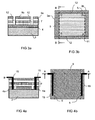
On a représenté sur les
Dans une première phase, ainsi que représenté sur les
Dans une seconde phase du procédé on réalise, en bordure de deux côtés opposés 3a du substrat verrier 3, un margeage rectiligne 5 parallèle à ces derniers.In a second phase of the process is carried out, along two
On entendra par margeage dans le présent texte, une découpe faite à travers certaines des couches du dispositif, dont la largeur sera suffisante pour que chaque partie d'une couche découpée soit isolée électriquement de l'autre partie. Le margeage sera dit total lorsqu'il s'étendra en profondeur à partir de la première des couches qui sera isolante sans traverser celle-ci, et traversera les différentes autres couches qui la séparent du substrat 3 jusqu'à atteindre celui-ci. Le margeage sera dit sélectif lorsqu'il s'étendra d'une couche donnée, en traversant celle-ci ainsi que les couches qui la séparent de l'électrode inférieure 4 jusqu'à cette dernière sans la traverser. Ces margeages seront préférentiellement réalisés, de façon connue, au moyen d'un faisceau laser, mais on pourra également faire appel à tout autre moyen permettant de les réaliser ainsi qu'exposé précédemment.Means in the present text will be understood to mean a cut made through some of the layers of the device, the width of which will be sufficient for each part of a cut layer to be electrically isolated from the other part. The margination will be said total when it will extend in depth from the first of the layers which will be insulating without crossing it, and will cross the various other layers which separate it from the
Ainsi que représenté (en traits pointillés) sur la
Chacun des deux margeages effectués partage ainsi la surface de l'électrode inférieure 4 en deux zones, à savoir une première zone 4a dite zone libre et une seconde zone 4b dite zone active, qui est commune aux deux margeages, et qui contient la zone qui sera la surface active CDEF du dispositif, c'est-à-dire la surface dont le niveau de transmission de la lumière sera contrôlé, ainsi qu'exposé ci-après.Each of the two margeages thus shares the surface of the
On dépose ensuite, ainsi que représenté sur les
Dans la mesure où la première couche 7a déposée après la réalisation des deux margeages 5 de type total est une couche isolante, il en résulte que les zones 4a et 4b sont non seulement isolées électriquement l'une de l'autre mais également des autres couches de l'empilement.Insofar as the
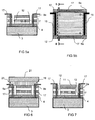
On réalise ensuite, ainsi que représenté sur les
On constate que chacune des zones libres 4a définie par chaque margeage total et chacune des zones libres 9a définie par chaque margeage sélectif est isolée électriquement d'une part des autres zones libres 4a et 9a et, d'autre part, des zones actives respectives 4b et 9b des électrodes inférieure et supérieure contenant la surface active CDEF du dispositif. Chacune de ces zones libres d'une électrode peut donc être réunie à une zone active de l'autre électrode sans causer de court-circuit.It can be seen that each of the
Le dispositif 1 permet donc, ainsi que représenté sur la
Une fois les barrettes de connexion 15 et 17 raccordées par soudure on pourra terminer l'empilement de façon classique, ainsi que représenté sur la
Dans ce mode de mise en oeuvre non suivant l'invention la surface active CDEF du dispositif est délimitée par les margeages de types total 5 (en traits pointillés sur le dessin) et de type sélectif 12 (en traits continus sur le dessin). Le dispositif 1 permet de réduire à un minimum les surfaces des zones libres au droit desquelles s'effectuent les connexions, favorisant ainsi la surface active du dispositif par rapport aux solutions de l'état antérieur de la technique.In this mode of implementation not according to the invention, the active surface CDEF of the device is delimited by the margins of total types 5 (in dashed lines on the drawing) and selective type 12 (in solid lines on the drawing). The
Bien entendu, le dispositif pourra ne pas être feuilleté et l'on pourra alors terminer l'empilement par le dépôt dune couche 11 de protection contre l'humidité, qui, ainsi que représenté sur la
Par ailleurs, on sait que lorsque l'on commande une variation de transmission de la surface active, par exemple une variation de transparence, celle-ci ne se traduit pas par une variation uniforme immédiate de densité de l'ensemble de cette surface active. En effet, pour des problèmes liés notamment à la résistivité des différentes couches électrochrome concernées, ainsi qu'à une différence de résistivité des électrodes supérieure et inférieure, la variation géométrique dans le temps de la transparence de la surface active, dénommée ci-après profil d'occultation, peut prendre différents aspects en fonction de la disposition des barrettes de connexion 15 et 17 sur les électrodes, ainsi qu'exposé ci-après.Moreover, it is known that when controlling a transmission variation of the active surface, for example a variation in transparency, this does not result in an immediate uniform density variation of the whole of this active surface. Indeed, for problems related in particular to the resistivity of the various electrochromic layers concerned, as well as to a resistivity difference of the upper and lower electrodes, the geometric variation in time of the transparency of the active surface, hereinafter referred to as the profile occultation, can take different aspects depending on the arrangement of the terminal strips 15 and 17 on the electrodes, as explained below.
La technique de margeage et de soudure exposée précédemment permet au concepteur de réaliser avec la plus grande liberté des dispositifs électrochromes dont les barrettes de connexion peuvent avoir des formes et des dispositions sur les électrodes qui sont fonction du profil d'occultation que l'on souhaite obtenir.The technique of margin and soldering previously described allows the designer to achieve with the greatest freedom electrochromic devices whose connection strips can have shapes and arrangements on the electrodes that are a function of the occultation profile that is desired get.
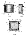
Ainsi, dans la disposition des barrettes de connexion adoptée précédemment on obtient un profil d'occultation en forme de rideau se déplaçant des bords 3a vers le centre, qui est représenté de façon schématique sur la
On peut également, de façon à obtenir un profil d'occultation plus régulier, adopter suivant l'invention une configuration du type de celle représentée sur la
Pour obtenir celle-ci, après le dépôt sur le substrat 3 de la couche 4 formant l'électrode inférieure, et ainsi qu'expliqué précédemment, on réalise un margeage total 5 à travers cette dernière, dans chacun des angles du substrat 3 (traits pointillés sur la figure), de façon à former dans celle-ci une zone libre 4a en forme d'équerre. On dépose ensuite les diverses couches fonctionnelles électrochromes 7 et la couche 9 formant l'électrode supérieure. On réalise ensuite au travers de celle-ci un margeage sélectif 12 (représenté en trais continus sur la figure) en traversant les couches déposées jusqu'à l'électrode inférieure 4 et sans traverser celle-ci. On donne à ce margeage 12 la forme d'une ligne continue fermée en forme de rectangle qui se situe en périphérie du substrat 3 et est centrée au milieu de chacun des côtés de celui-ci et qui partage la surface de l'électrode supérieure en deux zones, à savoir une zone libre 9a et une zone active 9b contenant la surface active CDEF du dispositif.To obtain this, after the deposition on the
On aurait pu également, ainsi que représenté sur la
Dans une autre variante non suivant l'invention, qui est représentée sur la
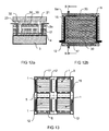
On a ainsi représenté sur la
A cet effet la partie centrale du substrat, en l'espèce de forme carrée, est subdivisée en quatre surfaces actives CDEF contiguës. Pour ce faire on a réalisé un margeage total au travers de l'électrode inférieure 4, délimitant ainsi au niveau de celle-ci une zone libre centrale 4a en forme de croix (représentée en traits pointillés sur la
La présente invention permet ainsi à la fois de supprimer du processus de fabrication des dispositifs électrochrome l'étape critique de mise en place et de retrait des adhésifs de masquage, ce qui se traduit par un gain de temps important, tout en en permettant d'améliorer la fiabilité dans le temps de ces dispositifs en permettant de relier leurs électrodes par soudure aux moyens de connexion. Elle permet de plus, en permettant de diminuer le courant de fuite dans des proportions importantes, de réaliser un dispositif électrochrome présentant un temps de réponse réduit et une plus faible consommation électrique. Elle permet enfin de rendre maximale la surface active CDEF du dispositif par rapport aux dimensions du substrat support et de contrôler la forme du profil d'occultation du dispositif.The present invention thus makes it possible at the same time to eliminate from the manufacturing process of the electrochromic devices the critical step of setting up and removing the masking adhesives, which results in a significant saving of time, while at the same time allowing to improve the reliability over time of these devices by making it possible to connect their electrodes by welding to the connection means. It also allows, by reducing the leakage current in large proportions, to achieve an electrochromic device having a reduced response time and lower power consumption. Finally, it makes it possible to maximize the active surface CDEF of the device relative to the dimensions of the support substrate and to control the shape of the concealment profile of the device.
La présente invention est également applicable aux dispositifs électrochromes dans lesquels, afin d'augmenter la conductivité de l'électrode supérieure on adjoint à celle-ci un réseau de fils conducteurs parallèles.The present invention is also applicable to electrochromic devices in which, in order to increase the conductivity of the upper electrode, there is added thereto an array of parallel conductive wires.
En effet on sait que l'on fait appel habituellement pour constituer les électrodes inférieure et supérieure des dispositifs électrochromes, à un matériau d'oxyde métallique dopé tel que l'oxyde d'étain dopé au fluor (SnO2 :F) ou l'oxyde d'indium dopé à l'étain (ITO) que l'on peut déposer sur différents substrats à chaud, notamment par pyrolyse sur du verre, comme la technique dite CVD, ou à froid notamment par des techniques sous vide de pulvérisation cathodique.In fact, it is known that the electrodes of the lower and upper electrodes of electrochromic devices are usually used to form a doped metal oxide material such as fluorine-doped tin oxide (SnO 2 : F) or indium oxide doped with tin (ITO) that can be deposited on various substrates hot, especially by pyrolysis on glass, as the so-called CVD technique, or cold in particular by sputtering vacuum cathodic techniques.
On a constaté que, dans les épaisseurs où elles restent transparentes, les couches à base de ces matériaux ne sont pas suffisamment conductrices du courant électrique, si bien que lorsque l'on applique entre leurs bornes la tension électrique appropriée pour provoquer la modification de changement d'état nécessaire à une modification de leur transmission, elles augmentent le temps de réponse du système, ou temps de commutation.It has been found that, in the thicknesses where they remain transparent, the layers based on these materials are not sufficiently conductive of the electric current, so that when the appropriate electrical voltage is applied between their terminals to cause the modification of change. of state necessary to modify their transmission, they increase the response time of the system, or switching time.
Plus précisément, dans le cas par exemple où les deux couches électroconductrices sont constituées d'oxyde d'indium dopé à l'étain (ITO), la résistivité de la couche de base, ou couche inférieure, qui est de l'ordre de 3 à 5 Ω/carré passe à 60-70 Ω/carré pour la couche supérieure en raison de sa plus faible épaisseur. On sait en effet que si la couche de base a une épaisseur de l'ordre de 500 nm, la couche supérieure quant à elle n'a qu'une épaisseur de l'ordre de 100 nm et ceci pour des raisons essentiellement liées à la contrainte mécanique générée dans l'empilement.More specifically, in the case for example where the two electroconductive layers consist of tin-doped indium oxide (ITO), the resistivity of the base layer, or lower layer, which is of the order of 3 at 5 Ω / squared goes to 60-70 Ω / squared for the top layer because of its smaller thickness. It is known that if the base layer has a thickness of the order of 500 nm, the upper layer has a thickness of the order of 100 nm and this for reasons essentially related to the mechanical stress generated in the stack.
Cette différence de résistivité entre les couches inférieure et supérieure est à l'origine du ralentissement du temps de commutation du dispositif, c'est-à-dire du temps nécessaire pour que le système passe de son état le plus transparent à son état le plus opaque. Un tel ralentissement contribue de plus à la formation du phénomène de « halo » mentionné précédemment.This difference in resistivity between the lower and upper layers is at the origin of the slowing down of the switching time of the device, that is to say the time required for the system to go from its most transparent state to its most opaque. Such slowing further contributes to the formation of the phenomenon of "halo" mentioned above.
Pour pallier un tel inconvénient on a proposé, dans la demande
Ainsi que représenté sur les
On peut également suivant l'invention réaliser sur un même substrat support plusieurs dispositifs électrochromes 1 qui, en fin de réalisation, seront séparés par découpe du substrat suivant des lignes de découpe 34 représentées en traits mixtes sur la
Un tel exemple permet de ne réaliser que quatre margeages de type total et quatre margeages de type sélectif pour quatre dispositifs, ce qui représente une simplification et un gain de temps au niveau de la fabrication.Such an example makes it possible to realize only four margeages of the total type and four margeages of selective type for four devices, which represents a simplification and a saving of time at the manufacturing level.
Claims (14)
- Electrochromic device having controlled transmission or reflection of at least one electrically controllable active area (CDEF), having, on a carrier substrate (3), a multilayer stack comprising at least, in succession, a layer forming a lower electrically conductive electrode (4), various functional layers (7) at least one of which is an electrochromic layer, at least one (6, 7a) of these layers being electrically insulating, and an upper electrically conductive electrode (9), in which device:- at least one partition (5), denoted "total", extends from the insulating layer (6, 7a) without passing through it, and passes through the layer(s) (4,2) separating the insulating layer from the substrate (3), this total partition (5) dividing the surface of the lower electrode (4) into two regions electrically isolated from each other, namely a free region (4a), in line with which the upper electrode (9) is soldered to a first current-supply connector (15), and an active region (4b) containing the active area (CDEF);
and- at least one partition (12), denoted "selective", passes through the upper electrode (9) and the various layers separating the upper electrode from the lower electrode (4) without passing through the latter, this selective partition (12) dividing the surface of the upper electrode (9) into two regions electrically isolated from each other, namely a free region (9a) on which a second current-supply connector (17) is deposited, which connector is soldered to the active region (4b) of the lower electrode (4), and an active region (9b) containing the active area (CDEF), and characterized in that
the free region (4a) of the lower electrode (4) is soldered to the first current-supply connector (15)
and in that the total partitions (5) are produced in the four corners of the substrate (3) so as to constitute substantially square free regions (4a) and in that the selective partitions (12) are produced substantially in the middle of the periphery of at least three of the four edges of said device so as to constitute substantially rectangular free regions (9a). - Controlled-transmission electrochromic device according to Claim 1, characterized in that the carrier substrate (3) has a glazing function and, in particular, is made of glass or plastic.
- Controlled-transmission electrochromic device according to one of the preceding claims, characterized in that the upper electrode (9) is covered with at least one moisture protection layer (11), the latter being penetrated by said selective partition (12).
- Controlled-transmission electrochromic device according to one of the preceding claims, characterized in that at least one of the electrodes (4, 9) is formed from at least one indium tin oxide (ITO) layer.
- Controlled-transmission electrochromic device according to one of the preceding claims, characterized in that the upper electrode (9) is in contact with an array of fine electrically conducting wires (30), connected to the first (current-supply) connector (15).
- Controlled-transmission electrochromic device according to Claim 5, characterized in that the array of wires (30) is supported by a support (32) particularly one made of a thermoplastic polymer, such as, for example, polyurethane or polyvinyl butyral (PVB).
- Controlled-transmission electrochromic device according to one of the preceding claims, characterized in that the free regions (4a, 9) defined by the total partitions (5) and selective partitions (12) are located on the periphery of said device.
- Controlled-transmission electrochromic device according to Claim 7, characterized in that the substrate (3) is rectangular shaped and in that the total partitions (5) and selective partitions (12) are respectively produced so as to be parallel with opposed sides (3a, 3b) of the substrate (3).
- Process for fabricating an electrochromic device having controlled transmission or reflection of at least one electrically controllable active area (CDEF), having on a carrier substrate (3), a multilayer stack comprising at least, in succession, an electrically conductive layer forming a lower electrode (4), various functional layers at least one of which is an electrochromic layer, at least one of these layers being electrically insulating, and an electrically conductive layer forming an upper electrode (9), comprising the steps consisting in:- depositing, onto at least part of the surface of the substrate (3), at least one electrically conductive layer forming the lower electrode (4), and the layers preceding said electrically insulating layer;- producing, starting from the electrically insulating layer, without passing through it, at least one total partition (5) of the layer(s) separating the insulating layer from the substrate (3), each total partition (5) dividing the surface of the lower electrode (4) into two regions electrically isolated from each other, namely a free region (4a), and an active region (4b) containing the active area (CDEF), the total partitions (5) being produced in the four corners of the substrate (3) so as to constitute substantially square free regions (4a);- depositing, onto the free and the active regions (4a, 4b), the electrically insulating layer (7a), the various other functional layers (7) and the electrically conductive layer forming the upper electrode (9);- producing at least one selective partition (12) through the upper electrode and through the various layers separating the upper electrode from the lower electrode (4) without passing through the latter, each selective partition (12) dividing the surface of the upper electrode (9) into two regions electrically isolated from each other, namely a free region (9a) and an active region (9b) containing the active area (CDEF), the selective partitions (12) being produced substantially in the middle of the periphery of at least three of the four edges of said device so as to constitute substantially rectangular free regions (9a);- soldering a first current-supply connector (15) to the active region (9b) of the upper electrode (9) and to the free region (4a) of the lower electrode (4); and- soldering a second current-supply connector (17) to the free region (9a) of the upper electrode (9) and to the active region (4b) of the lower electrode located in line with the latter.
- Process for fabricating a controlled-transmission electrochromic device according to Claim 9, characterized in that at least one of the solder joints is ultrasonically soldered.
- Process for fabricating a controlled-transmission electrochromic device according to Claim 9 or 10, characterized in that at least one of the partitions (5, 12) is produced by means of a laser beam.
- Process for fabricating a controlled-transmission electrochromic device according to one of Claims 9 to 11, in which several electrochromic devices according to one of Claims 1 to 8 are produced on one and the same carrier substrate, characterized in that, once said devices are completed, the carrier substrate and all the layers deposited thereon are cut so as to constitute specific devices.
- Electrochromic glazing, characterized in that it includes an electrochromic device according to one of Claims 1 to 8, in particular having a variable light and/or energy transmission and/or reflection, with the substrate or at least part of the substrates transparent or partially transparent, made of plastic, preferably mounted as multiple and/or laminated glazing or as double glazing.
- Use of the glazing according to Claim 13 as architectural glazing, as automotive glazing, as glazing for industrial vehicles or for public transport - by rail, sea or air - for agricultural vehicles, for construction site machinery, for rear-view or wing mirrors or for other mirrors, for displays and signage and for camera shutters.
Applications Claiming Priority (2)
| Application Number | Priority Date | Filing Date | Title |
|---|---|---|---|
| FR0952491A FR2944610B1 (en) | 2009-04-16 | 2009-04-16 | ELECTROCHROME DEVICE HAVING CONTROLLED TRANSPARENCY |
| PCT/FR2010/050723 WO2010119228A1 (en) | 2009-04-16 | 2010-04-15 | Electrochrome device with controlled transparency |
Publications (2)
| Publication Number | Publication Date |
|---|---|
| EP2419787A1 EP2419787A1 (en) | 2012-02-22 |
| EP2419787B1 true EP2419787B1 (en) | 2014-10-01 |
Family
ID=41171114
Family Applications (1)
| Application Number | Title | Priority Date | Filing Date |
|---|---|---|---|
| EP10723677.0A Active EP2419787B1 (en) | 2009-04-16 | 2010-04-15 | Electrochromic apparatus with controlled transmission |
Country Status (8)
| Country | Link |
|---|---|
| US (1) | US8405896B2 (en) |
| EP (1) | EP2419787B1 (en) |
| JP (1) | JP5646597B2 (en) |
| KR (1) | KR20120013384A (en) |
| CN (1) | CN102460292B (en) |
| ES (1) | ES2525802T3 (en) |
| FR (1) | FR2944610B1 (en) |
| WO (1) | WO2010119228A1 (en) |
Cited By (1)
| Publication number | Priority date | Publication date | Assignee | Title |
|---|---|---|---|---|
| CN105644443A (en) * | 2016-03-04 | 2016-06-08 | 京东方科技集团股份有限公司 | Back sight system for automobile and automobile |
Families Citing this family (42)
| Publication number | Priority date | Publication date | Assignee | Title |
|---|---|---|---|---|
| US9782949B2 (en) | 2008-05-30 | 2017-10-10 | Corning Incorporated | Glass laminated articles and layered articles |
| US9007674B2 (en) | 2011-09-30 | 2015-04-14 | View, Inc. | Defect-mitigation layers in electrochromic devices |
| US12496809B2 (en) | 2010-11-08 | 2025-12-16 | View Operating Corporation | Electrochromic window fabrication methods |
| US10429712B2 (en) * | 2012-04-20 | 2019-10-01 | View, Inc. | Angled bus bar |
| US12403676B2 (en) | 2011-12-12 | 2025-09-02 | View Operating Corporation | Thin-film devices and fabrication |
| CA2859023C (en) * | 2011-12-12 | 2023-08-22 | View, Inc. | Thin-film devices and fabrication |
| US12061402B2 (en) | 2011-12-12 | 2024-08-13 | View, Inc. | Narrow pre-deposition laser deletion |
| US20130222877A1 (en) | 2012-02-28 | 2013-08-29 | Sage Electrochromics, Inc. | Multi-zone electrochromic devices |
| US20130222878A1 (en) * | 2012-02-28 | 2013-08-29 | Sage Electrochromics, Inc. | Multi-zone electrochromic devices |
| CN104662471A (en) * | 2012-06-05 | 2015-05-27 | Sage电致变色显示有限公司 | Electrical feed-through spacer and connectivity |
| KR101980239B1 (en) * | 2012-12-28 | 2019-05-20 | 엘지디스플레이 주식회사 | Organic Light Emitting diode display and method of manufacturing the same |
| US9013778B2 (en) * | 2013-03-06 | 2015-04-21 | Sage Electrochromics, Inc. | Laser cuts to reduce electrical leakage |
| JP6285971B2 (en) * | 2013-03-08 | 2018-02-28 | セイジ・エレクトロクロミクス,インコーポレイテッド | Electrochromic device with multiple independently controllable zones and internal bus bars |
| EP3011387A4 (en) | 2013-06-18 | 2016-11-30 | View Inc | ELECTROCHROMIC DEVICES IN NON-RECTANGULAR FORMS |
| US9152001B2 (en) * | 2013-07-25 | 2015-10-06 | Sage Electrochromics, Inc. | Electrochromic devices having improved structure for reducing current leakage across lower transparent conductor layers |
| US9778531B2 (en) | 2013-07-29 | 2017-10-03 | Chromogenics Ab | Contacting of electrochromic devices |
| US20150153622A1 (en) | 2013-12-03 | 2015-06-04 | Sage Electrochromics, Inc. | Methods for producing lower electrical isolation in electrochromic films |
| JP6452734B2 (en) * | 2014-06-17 | 2019-01-16 | セイジ・エレクトロクロミクス,インコーポレイテッド | Moisture resistant electrochromic device |
| US12235560B2 (en) | 2014-11-25 | 2025-02-25 | View, Inc. | Faster switching electrochromic devices |
| CN107533267A (en) | 2015-03-20 | 2018-01-02 | 唯景公司 | Switch low defect electrochromic more quickly |
| JP6583803B2 (en) * | 2016-03-28 | 2019-10-02 | パナソニックIpマネジメント株式会社 | Electrochromic device |
| JPWO2017169243A1 (en) * | 2016-03-31 | 2019-02-28 | 株式会社村上開明堂 | Solid-type EC mirror and manufacturing method thereof |
| US9998681B2 (en) * | 2016-06-28 | 2018-06-12 | Gopro, Inc. | Electronic iris for a camera |
| US10850666B1 (en) * | 2016-08-09 | 2020-12-01 | Apple Inc. | Windows with active layers |
| US10247997B2 (en) | 2016-08-16 | 2019-04-02 | Cardinal Cg Company | Switchable hydride smart window and the methods for producing the same |
| WO2018119095A1 (en) | 2016-12-22 | 2018-06-28 | Sage Electrochromics, Inc. | Apparatus including an electrochromic device configured to maintain a continuously graded transmission state |
| CN110337716A (en) | 2017-02-27 | 2019-10-15 | Sage电致变色显示有限公司 | The method of electrical equipment and formation electrical equipment including substrate and transparency conducting layer |
| CN108519709A (en) * | 2018-06-01 | 2018-09-11 | Oppo广东移动通信有限公司 | Electrochromic mother board, electrochromic unit, casing and electronic equipment |
| CN108646495A (en) * | 2018-07-17 | 2018-10-12 | 合肥威驰科技有限公司 | For the vehicles can subregion change colour dimming glass |
| CN109031836B (en) * | 2018-09-06 | 2021-06-29 | 江苏天贯碳纳米材料有限公司 | ITO glass conducting layer segmentation method and ITO conducting glass |
| TWI734299B (en) * | 2018-12-31 | 2021-07-21 | 美商塞奇電致變色公司 | Apparatus to maintain a continuously graded transmission state |
| US20210026163A1 (en) * | 2019-07-25 | 2021-01-28 | Gentex Corporation | Segmented variable controlled electro-optic element |
| JP7486578B2 (en) * | 2019-10-18 | 2024-05-17 | ビトロ フラット グラス エルエルシー | Electrochromic devices and methods of making and operating same |
| EP4202542A4 (en) * | 2020-09-04 | 2024-12-04 | Shenzhen Guangyi Tech Co., Ltd. | ELECTROCHROMIC DEVICE AND ELECTRONIC DEVICE |
| CN114815431B (en) * | 2021-01-22 | 2025-08-08 | 深圳市光羿科技有限公司 | Electrochromic device and electronic equipment |
| CN112558371B (en) * | 2020-12-08 | 2022-12-16 | 深圳市光羿科技有限公司 | Color changing device and control method thereof |
| CN114779548B (en) * | 2021-01-22 | 2025-06-10 | 深圳市光羿科技有限公司 | Electrochromic device and electronic equipment |
| CN116830031A (en) * | 2021-02-04 | 2023-09-29 | 圣戈本玻璃法国公司 | Methods of manufacturing electrochromic devices, electrochromic devices and insulating vitreous bodies |
| CN112904636B (en) | 2021-02-06 | 2023-03-24 | 深圳市光羿科技有限公司 | Electrochromic device and electronic terminal comprising same |
| CN113189822A (en) * | 2021-04-23 | 2021-07-30 | 广东省科学院新材料研究所 | Electrochromic device and preparation method thereof |
| CN115509054B (en) * | 2021-06-07 | 2025-06-10 | 深圳市光羿科技有限公司 | Electrochromic device and preparation method and application thereof |
| WO2022268395A1 (en) * | 2021-06-21 | 2022-12-29 | Saint-Gobain Glass France | Segmented multilayer film with electrically controllable optical properties |
Family Cites Families (7)
| Publication number | Priority date | Publication date | Assignee | Title |
|---|---|---|---|---|
| JPS6214118A (en) * | 1985-07-12 | 1987-01-22 | Canon Inc | electrochromic device |
| JPS63305326A (en) * | 1987-06-08 | 1988-12-13 | Ichikoh Ind Ltd | EC anti-glare mirror for automobiles |
| US5530581A (en) * | 1995-05-31 | 1996-06-25 | Eic Laboratories, Inc. | Protective overlayer material and electro-optical coating using same |
| US5724175A (en) * | 1997-01-02 | 1998-03-03 | Optical Coating Laboratory, Inc. | Electrochromic device manufacturing process |
| FR2811778B1 (en) * | 2000-07-13 | 2003-06-20 | Saint Gobain | ELECTROCHEMICAL DEVICE OF THE ELECTROCHROMIC TYPE OR PHOTOVOLTAIC DEVICE AND ITS ELECTRICAL CONNECTION MEANS |
| FR2874100B1 (en) * | 2004-08-04 | 2006-09-29 | Saint Gobain | ELECTROCHEMICAL SYSTEM COMPRISING AT LEAST ONE PARTIAL MARGIN AREA |
| US7688495B2 (en) * | 2006-03-03 | 2010-03-30 | Gentex Corporation | Thin-film coatings, electro-optic elements and assemblies incorporating these elements |
-
2009
- 2009-04-16 FR FR0952491A patent/FR2944610B1/en not_active Expired - Fee Related
-
2010
- 2010-04-15 KR KR1020117027157A patent/KR20120013384A/en not_active Withdrawn
- 2010-04-15 EP EP10723677.0A patent/EP2419787B1/en active Active
- 2010-04-15 ES ES10723677.0T patent/ES2525802T3/en active Active
- 2010-04-15 CN CN201080026989.3A patent/CN102460292B/en not_active Expired - Fee Related
- 2010-04-15 WO PCT/FR2010/050723 patent/WO2010119228A1/en not_active Ceased
- 2010-04-15 JP JP2012505209A patent/JP5646597B2/en not_active Expired - Fee Related
- 2010-04-15 US US12/922,341 patent/US8405896B2/en not_active Expired - Fee Related
Cited By (2)
| Publication number | Priority date | Publication date | Assignee | Title |
|---|---|---|---|---|
| CN105644443A (en) * | 2016-03-04 | 2016-06-08 | 京东方科技集团股份有限公司 | Back sight system for automobile and automobile |
| CN105644443B (en) * | 2016-03-04 | 2018-12-28 | 京东方科技集团股份有限公司 | A kind of back-sight visual system and automobile for automobile |
Also Published As
| Publication number | Publication date |
|---|---|
| JP2012524290A (en) | 2012-10-11 |
| CN102460292A (en) | 2012-05-16 |
| KR20120013384A (en) | 2012-02-14 |
| US20120019889A1 (en) | 2012-01-26 |
| JP5646597B2 (en) | 2014-12-24 |
| FR2944610B1 (en) | 2011-06-24 |
| EP2419787A1 (en) | 2012-02-22 |
| US8405896B2 (en) | 2013-03-26 |
| FR2944610A1 (en) | 2010-10-22 |
| WO2010119228A1 (en) | 2010-10-21 |
| ES2525802T3 (en) | 2014-12-30 |
| CN102460292B (en) | 2014-07-30 |
Similar Documents
| Publication | Publication Date | Title |
|---|---|---|
| EP2419787B1 (en) | Electrochromic apparatus with controlled transmission | |
| EP2419788B1 (en) | Electrochromic device with controlled transmission | |
| EP1776612B1 (en) | Electrochemical system comprising at least one partial making up zone | |
| CA2637247C (en) | Transparent glazing provided with laminated heating system | |
| EP1803327B1 (en) | Transparent window pane provided with a resistive heating coating | |
| EP2263118B1 (en) | Electrochromic device including a meshing | |
| EP2047325B1 (en) | Glass type electrochemical/ electrically controllable device with variable optical and/or energetic characteristic | |
| FR2962818A1 (en) | ELECTROCHEMICAL DEVICE HAVING ELECTRO - CONTROLLABLE OPTICAL AND / OR ENERGY TRANSMISSION PROPERTIES. | |
| FR2791147A1 (en) | ELECTROCHEMICAL DEVICE OF THE ELECTROCOMMANDABLE DEVICE TYPE WITH VARIABLE OPTICAL AND / OR ENERGY PROPERTIES | |
| EP1299768A1 (en) | Electrochemical device such as electrochromic or photovoltaic device and electrical connection means thereof | |
| FR2899631A1 (en) | LAMINATED GLAZING AND ITS MEANS FOR SEALING AND PERIPHERAL REINFORCEMENT | |
| EP1366387A1 (en) | Electrically controllable device with variable optical and/or energy properties | |
| WO2007057461A1 (en) | Laminated glazing and a method for the production thereof | |
| WO2007057463A1 (en) | Laminated glazing and a method for the production thereof |
Legal Events
| Date | Code | Title | Description |
|---|---|---|---|
| PUAI | Public reference made under article 153(3) epc to a published international application that has entered the european phase |
Free format text: ORIGINAL CODE: 0009012 |
|
| 17P | Request for examination filed |
Effective date: 20111116 |
|
| AK | Designated contracting states |
Kind code of ref document: A1 Designated state(s): AT BE BG CH CY CZ DE DK EE ES FI FR GB GR HR HU IE IS IT LI LT LU LV MC MK MT NL NO PL PT RO SE SI SK SM TR |
|
| RIN1 | Information on inventor provided before grant (corrected) |
Inventor name: VALENTIN, EMMANUEL Inventor name: LAMINE, DRISS Inventor name: DUBRENAT, SAMUEL |
|
| RAP1 | Party data changed (applicant data changed or rights of an application transferred) |
Owner name: SAGE ELECTROCHROMICS, INC. |
|
| DAX | Request for extension of the european patent (deleted) | ||
| 17Q | First examination report despatched |
Effective date: 20121018 |
|
| 18D | Application deemed to be withdrawn |
Effective date: 20130301 |
|
| D18D | Application deemed to be withdrawn (deleted) | ||
| GRAP | Despatch of communication of intention to grant a patent |
Free format text: ORIGINAL CODE: EPIDOSNIGR1 |
|
| INTG | Intention to grant announced |
Effective date: 20140428 |
|
| GRAS | Grant fee paid |
Free format text: ORIGINAL CODE: EPIDOSNIGR3 |
|
| GRAA | (expected) grant |
Free format text: ORIGINAL CODE: 0009210 |
|
| AK | Designated contracting states |
Kind code of ref document: B1 Designated state(s): AT BE BG CH CY CZ DE DK EE ES FI FR GB GR HR HU IE IS IT LI LT LU LV MC MK MT NL NO PL PT RO SE SI SK SM TR |
|
| REG | Reference to a national code |
Ref country code: CH Ref legal event code: EP Ref country code: AT Ref legal event code: REF Ref document number: 689807 Country of ref document: AT Kind code of ref document: T Effective date: 20141015 |
|
| REG | Reference to a national code |
Ref country code: IE Ref legal event code: FG4D Free format text: LANGUAGE OF EP DOCUMENT: FRENCH |
|
| REG | Reference to a national code |
Ref country code: DE Ref legal event code: R096 Ref document number: 602010019238 Country of ref document: DE Effective date: 20141113 |
|
| REG | Reference to a national code |
Ref country code: CH Ref legal event code: NV Representative=s name: KIRKER AND CIE S.A., CH |
|
| REG | Reference to a national code |
Ref country code: ES Ref legal event code: FG2A Ref document number: 2525802 Country of ref document: ES Kind code of ref document: T3 Effective date: 20141230 |
|
| REG | Reference to a national code |
Ref country code: NL Ref legal event code: VDEP Effective date: 20141001 |
|
| REG | Reference to a national code |
Ref country code: AT Ref legal event code: MK05 Ref document number: 689807 Country of ref document: AT Kind code of ref document: T Effective date: 20141001 |
|
| REG | Reference to a national code |
Ref country code: LT Ref legal event code: MG4D |
|
| PG25 | Lapsed in a contracting state [announced via postgrant information from national office to epo] |
Ref country code: NL Free format text: LAPSE BECAUSE OF FAILURE TO SUBMIT A TRANSLATION OF THE DESCRIPTION OR TO PAY THE FEE WITHIN THE PRESCRIBED TIME-LIMIT Effective date: 20141001 |
|
| PG25 | Lapsed in a contracting state [announced via postgrant information from national office to epo] |
Ref country code: NO Free format text: LAPSE BECAUSE OF FAILURE TO SUBMIT A TRANSLATION OF THE DESCRIPTION OR TO PAY THE FEE WITHIN THE PRESCRIBED TIME-LIMIT Effective date: 20150101 Ref country code: IS Free format text: LAPSE BECAUSE OF FAILURE TO SUBMIT A TRANSLATION OF THE DESCRIPTION OR TO PAY THE FEE WITHIN THE PRESCRIBED TIME-LIMIT Effective date: 20150201 Ref country code: LT Free format text: LAPSE BECAUSE OF FAILURE TO SUBMIT A TRANSLATION OF THE DESCRIPTION OR TO PAY THE FEE WITHIN THE PRESCRIBED TIME-LIMIT Effective date: 20141001 Ref country code: PT Free format text: LAPSE BECAUSE OF FAILURE TO SUBMIT A TRANSLATION OF THE DESCRIPTION OR TO PAY THE FEE WITHIN THE PRESCRIBED TIME-LIMIT Effective date: 20150202 Ref country code: FI Free format text: LAPSE BECAUSE OF FAILURE TO SUBMIT A TRANSLATION OF THE DESCRIPTION OR TO PAY THE FEE WITHIN THE PRESCRIBED TIME-LIMIT Effective date: 20141001 Ref country code: CZ Free format text: LAPSE BECAUSE OF FAILURE TO SUBMIT A TRANSLATION OF THE DESCRIPTION OR TO PAY THE FEE WITHIN THE PRESCRIBED TIME-LIMIT Effective date: 20141001 |
|
| PG25 | Lapsed in a contracting state [announced via postgrant information from national office to epo] |
Ref country code: PL Free format text: LAPSE BECAUSE OF FAILURE TO SUBMIT A TRANSLATION OF THE DESCRIPTION OR TO PAY THE FEE WITHIN THE PRESCRIBED TIME-LIMIT Effective date: 20141001 Ref country code: SE Free format text: LAPSE BECAUSE OF FAILURE TO SUBMIT A TRANSLATION OF THE DESCRIPTION OR TO PAY THE FEE WITHIN THE PRESCRIBED TIME-LIMIT Effective date: 20141001 Ref country code: HR Free format text: LAPSE BECAUSE OF FAILURE TO SUBMIT A TRANSLATION OF THE DESCRIPTION OR TO PAY THE FEE WITHIN THE PRESCRIBED TIME-LIMIT Effective date: 20141001 Ref country code: CY Free format text: LAPSE BECAUSE OF FAILURE TO SUBMIT A TRANSLATION OF THE DESCRIPTION OR TO PAY THE FEE WITHIN THE PRESCRIBED TIME-LIMIT Effective date: 20141001 Ref country code: AT Free format text: LAPSE BECAUSE OF FAILURE TO SUBMIT A TRANSLATION OF THE DESCRIPTION OR TO PAY THE FEE WITHIN THE PRESCRIBED TIME-LIMIT Effective date: 20141001 Ref country code: LV Free format text: LAPSE BECAUSE OF FAILURE TO SUBMIT A TRANSLATION OF THE DESCRIPTION OR TO PAY THE FEE WITHIN THE PRESCRIBED TIME-LIMIT Effective date: 20141001 Ref country code: GR Free format text: LAPSE BECAUSE OF FAILURE TO SUBMIT A TRANSLATION OF THE DESCRIPTION OR TO PAY THE FEE WITHIN THE PRESCRIBED TIME-LIMIT Effective date: 20150102 |
|
| REG | Reference to a national code |
Ref country code: DE Ref legal event code: R097 Ref document number: 602010019238 Country of ref document: DE |
|
| PG25 | Lapsed in a contracting state [announced via postgrant information from national office to epo] |
Ref country code: SK Free format text: LAPSE BECAUSE OF FAILURE TO SUBMIT A TRANSLATION OF THE DESCRIPTION OR TO PAY THE FEE WITHIN THE PRESCRIBED TIME-LIMIT Effective date: 20141001 Ref country code: EE Free format text: LAPSE BECAUSE OF FAILURE TO SUBMIT A TRANSLATION OF THE DESCRIPTION OR TO PAY THE FEE WITHIN THE PRESCRIBED TIME-LIMIT Effective date: 20141001 Ref country code: DK Free format text: LAPSE BECAUSE OF FAILURE TO SUBMIT A TRANSLATION OF THE DESCRIPTION OR TO PAY THE FEE WITHIN THE PRESCRIBED TIME-LIMIT Effective date: 20141001 |
|
| PLBE | No opposition filed within time limit |
Free format text: ORIGINAL CODE: 0009261 |
|
| STAA | Information on the status of an ep patent application or granted ep patent |
Free format text: STATUS: NO OPPOSITION FILED WITHIN TIME LIMIT |
|
| 26N | No opposition filed |
Effective date: 20150702 |
|
| PG25 | Lapsed in a contracting state [announced via postgrant information from national office to epo] |
Ref country code: MC Free format text: LAPSE BECAUSE OF FAILURE TO SUBMIT A TRANSLATION OF THE DESCRIPTION OR TO PAY THE FEE WITHIN THE PRESCRIBED TIME-LIMIT Effective date: 20141001 Ref country code: LU Free format text: LAPSE BECAUSE OF FAILURE TO SUBMIT A TRANSLATION OF THE DESCRIPTION OR TO PAY THE FEE WITHIN THE PRESCRIBED TIME-LIMIT Effective date: 20150415 |
|
| REG | Reference to a national code |
Ref country code: IE Ref legal event code: MM4A |
|
| PG25 | Lapsed in a contracting state [announced via postgrant information from national office to epo] |
Ref country code: SI Free format text: LAPSE BECAUSE OF FAILURE TO SUBMIT A TRANSLATION OF THE DESCRIPTION OR TO PAY THE FEE WITHIN THE PRESCRIBED TIME-LIMIT Effective date: 20141001 |
|
| REG | Reference to a national code |
Ref country code: FR Ref legal event code: PLFP Year of fee payment: 7 |
|
| PG25 | Lapsed in a contracting state [announced via postgrant information from national office to epo] |
Ref country code: IE Free format text: LAPSE BECAUSE OF NON-PAYMENT OF DUE FEES Effective date: 20150415 |
|
| PG25 | Lapsed in a contracting state [announced via postgrant information from national office to epo] |
Ref country code: MT Free format text: LAPSE BECAUSE OF FAILURE TO SUBMIT A TRANSLATION OF THE DESCRIPTION OR TO PAY THE FEE WITHIN THE PRESCRIBED TIME-LIMIT Effective date: 20141001 |
|
| REG | Reference to a national code |
Ref country code: FR Ref legal event code: PLFP Year of fee payment: 8 |
|
| PG25 | Lapsed in a contracting state [announced via postgrant information from national office to epo] |
Ref country code: BG Free format text: LAPSE BECAUSE OF FAILURE TO SUBMIT A TRANSLATION OF THE DESCRIPTION OR TO PAY THE FEE WITHIN THE PRESCRIBED TIME-LIMIT Effective date: 20141001 Ref country code: SM Free format text: LAPSE BECAUSE OF FAILURE TO SUBMIT A TRANSLATION OF THE DESCRIPTION OR TO PAY THE FEE WITHIN THE PRESCRIBED TIME-LIMIT Effective date: 20141001 Ref country code: RO Free format text: LAPSE BECAUSE OF FAILURE TO SUBMIT A TRANSLATION OF THE DESCRIPTION OR TO PAY THE FEE WITHIN THE PRESCRIBED TIME-LIMIT Effective date: 20141001 Ref country code: HU Free format text: LAPSE BECAUSE OF FAILURE TO SUBMIT A TRANSLATION OF THE DESCRIPTION OR TO PAY THE FEE WITHIN THE PRESCRIBED TIME-LIMIT; INVALID AB INITIO Effective date: 20100415 |
|
| PG25 | Lapsed in a contracting state [announced via postgrant information from national office to epo] |
Ref country code: TR Free format text: LAPSE BECAUSE OF FAILURE TO SUBMIT A TRANSLATION OF THE DESCRIPTION OR TO PAY THE FEE WITHIN THE PRESCRIBED TIME-LIMIT Effective date: 20141001 |
|
| REG | Reference to a national code |
Ref country code: FR Ref legal event code: PLFP Year of fee payment: 9 |
|
| PG25 | Lapsed in a contracting state [announced via postgrant information from national office to epo] |
Ref country code: MK Free format text: LAPSE BECAUSE OF FAILURE TO SUBMIT A TRANSLATION OF THE DESCRIPTION OR TO PAY THE FEE WITHIN THE PRESCRIBED TIME-LIMIT Effective date: 20141001 |
|
| PGFP | Annual fee paid to national office [announced via postgrant information from national office to epo] |
Ref country code: IT Payment date: 20230310 Year of fee payment: 14 Ref country code: GB Payment date: 20230302 Year of fee payment: 14 Ref country code: BE Payment date: 20230315 Year of fee payment: 14 |
|
| P01 | Opt-out of the competence of the unified patent court (upc) registered |
Effective date: 20230515 |
|
| PGFP | Annual fee paid to national office [announced via postgrant information from national office to epo] |
Ref country code: FR Payment date: 20230421 Year of fee payment: 14 Ref country code: ES Payment date: 20230512 Year of fee payment: 14 |
|
| PGFP | Annual fee paid to national office [announced via postgrant information from national office to epo] |
Ref country code: DE Payment date: 20240306 Year of fee payment: 15 |
|
| PGFP | Annual fee paid to national office [announced via postgrant information from national office to epo] |
Ref country code: CH Payment date: 20240501 Year of fee payment: 15 |
|
| GBPC | Gb: european patent ceased through non-payment of renewal fee |
Effective date: 20240415 |
|
| REG | Reference to a national code |
Ref country code: BE Ref legal event code: MM Effective date: 20240430 |
|
| PG25 | Lapsed in a contracting state [announced via postgrant information from national office to epo] |
Ref country code: BE Free format text: LAPSE BECAUSE OF NON-PAYMENT OF DUE FEES Effective date: 20240430 |
|
| PG25 | Lapsed in a contracting state [announced via postgrant information from national office to epo] |
Ref country code: GB Free format text: LAPSE BECAUSE OF NON-PAYMENT OF DUE FEES Effective date: 20240415 |
|
| PG25 | Lapsed in a contracting state [announced via postgrant information from national office to epo] |
Ref country code: FR Free format text: LAPSE BECAUSE OF NON-PAYMENT OF DUE FEES Effective date: 20240430 |
|
| PG25 | Lapsed in a contracting state [announced via postgrant information from national office to epo] |
Ref country code: GB Free format text: LAPSE BECAUSE OF NON-PAYMENT OF DUE FEES Effective date: 20240415 Ref country code: FR Free format text: LAPSE BECAUSE OF NON-PAYMENT OF DUE FEES Effective date: 20240430 Ref country code: BE Free format text: LAPSE BECAUSE OF NON-PAYMENT OF DUE FEES Effective date: 20240430 |
|
| PG25 | Lapsed in a contracting state [announced via postgrant information from national office to epo] |
Ref country code: IT Free format text: LAPSE BECAUSE OF NON-PAYMENT OF DUE FEES Effective date: 20240415 |
|
| REG | Reference to a national code |
Ref country code: ES Ref legal event code: FD2A Effective date: 20250529 |
|
| PG25 | Lapsed in a contracting state [announced via postgrant information from national office to epo] |
Ref country code: ES Free format text: LAPSE BECAUSE OF NON-PAYMENT OF DUE FEES Effective date: 20240416 |
|
| REG | Reference to a national code |
Ref country code: DE Ref legal event code: R119 Ref document number: 602010019238 Country of ref document: DE |
|
| REG | Reference to a national code |
Ref country code: CH Ref legal event code: H13 Free format text: ST27 STATUS EVENT CODE: U-0-0-H10-H13 (AS PROVIDED BY THE NATIONAL OFFICE) Effective date: 20251125 |
|
| PG25 | Lapsed in a contracting state [announced via postgrant information from national office to epo] |
Ref country code: DE Free format text: LAPSE BECAUSE OF NON-PAYMENT OF DUE FEES Effective date: 20251104 |
|
| PG25 | Lapsed in a contracting state [announced via postgrant information from national office to epo] |
Ref country code: CH Free format text: LAPSE BECAUSE OF NON-PAYMENT OF DUE FEES Effective date: 20250430 |