EP2416186A1 - Lens - Google Patents
Lens Download PDFInfo
- Publication number
- EP2416186A1 EP2416186A1 EP10761506A EP10761506A EP2416186A1 EP 2416186 A1 EP2416186 A1 EP 2416186A1 EP 10761506 A EP10761506 A EP 10761506A EP 10761506 A EP10761506 A EP 10761506A EP 2416186 A1 EP2416186 A1 EP 2416186A1
- Authority
- EP
- European Patent Office
- Prior art keywords
- lens
- optical axis
- optical
- mold
- transferring
- Prior art date
- Legal status (The legal status is an assumption and is not a legal conclusion. Google has not performed a legal analysis and makes no representation as to the accuracy of the status listed.)
- Withdrawn
Links
Images



Classifications
-
- G—PHYSICS
- G02—OPTICS
- G02B—OPTICAL ELEMENTS, SYSTEMS OR APPARATUS
- G02B7/00—Mountings, adjusting means, or light-tight connections, for optical elements
- G02B7/02—Mountings, adjusting means, or light-tight connections, for optical elements for lenses
- G02B7/022—Mountings, adjusting means, or light-tight connections, for optical elements for lenses lens and mount having complementary engagement means, e.g. screw/thread
-
- B—PERFORMING OPERATIONS; TRANSPORTING
- B29—WORKING OF PLASTICS; WORKING OF SUBSTANCES IN A PLASTIC STATE IN GENERAL
- B29D—PRODUCING PARTICULAR ARTICLES FROM PLASTICS OR FROM SUBSTANCES IN A PLASTIC STATE
- B29D11/00—Producing optical elements, e.g. lenses or prisms
- B29D11/00009—Production of simple or compound lenses
- B29D11/00413—Production of simple or compound lenses made by moulding between two mould parts which are not in direct contact with one another, e.g. comprising a seal between or on the edges
-
- G—PHYSICS
- G02—OPTICS
- G02B—OPTICAL ELEMENTS, SYSTEMS OR APPARATUS
- G02B3/00—Simple or compound lenses
-
- G—PHYSICS
- G02—OPTICS
- G02B—OPTICAL ELEMENTS, SYSTEMS OR APPARATUS
- G02B5/00—Optical elements other than lenses
- G02B5/18—Diffraction gratings
-
- G—PHYSICS
- G11—INFORMATION STORAGE
- G11B—INFORMATION STORAGE BASED ON RELATIVE MOVEMENT BETWEEN RECORD CARRIER AND TRANSDUCER
- G11B7/00—Recording or reproducing by optical means, e.g. recording using a thermal beam of optical radiation by modifying optical properties or the physical structure, reproducing using an optical beam at lower power by sensing optical properties; Record carriers therefor
- G11B7/12—Heads, e.g. forming of the optical beam spot or modulation of the optical beam
- G11B7/135—Means for guiding the beam from the source to the record carrier or from the record carrier to the detector
-
- G—PHYSICS
- G11—INFORMATION STORAGE
- G11B—INFORMATION STORAGE BASED ON RELATIVE MOVEMENT BETWEEN RECORD CARRIER AND TRANSDUCER
- G11B7/00—Recording or reproducing by optical means, e.g. recording using a thermal beam of optical radiation by modifying optical properties or the physical structure, reproducing using an optical beam at lower power by sensing optical properties; Record carriers therefor
- G11B7/12—Heads, e.g. forming of the optical beam spot or modulation of the optical beam
- G11B7/135—Means for guiding the beam from the source to the record carrier or from the record carrier to the detector
- G11B7/1372—Lenses
- G11B7/1374—Objective lenses
Definitions
- the present invention relates to a lens with a NA of 0.7 or more in highly accurate shape.
- optical disc on which information is recorded/reproduced under the specifications that NA is 0.85 and a light source wavelength is 405 nm, namely, in the case of the so-called Blu-ray Disc (hereinafter, BD), it is possible to record information of 23 to 27 GB per layer for an optical disc with a diameter of 12 cm, which is same in size as DVD (NA is 0.6, wavelength of a light source is 650 nm, and memory capacity is 4.7 GB).
- This optical disc is referred as a high density optical disc in the present specification.
- an objective lens for use in an optical pickup apparatus there is disclosed an objective lens obtained by molding resin, for example, in Patent Literature 1.
- a connecting area is arranged on a portion on a lens surface which is outside from an intersection of the outermost ray within numerical aperture NA and the lens surface, in order to avoid defective molding of a lens.
- a thickness deviation ratio which will be described below
- excessively small thickness deviation ratio makes the flange thickness thick, and the effective aperture is hardly enlarged. Accordingly, in a high-NA lens with a large effective aperture, a lens design cannot be achieved in view of optics under the condition that the thickness deviation ratio is small.
- the present invention has been achieved in view of the above problem in the prior art, and is intended to provide a lens which allows to control defects caused in a molding process in a high-NA lens and which is easy to handle.
- a lens described in Claim 1 is a lens which is molded out of a resin material, comprises a flange section on a periphery and has a numerical aperture of 0.7 or more, characterized by comprising:
- the defective molding can be controlled by arranging the transition surface, the defective molding such as flow marks can be generated even when the transition surface is provided under the condition that d/t (which is referred as a thickness deviation ratio) is 4.1 or more.
- d/t which is referred as a thickness deviation ratio
- the thickness of a flange becomes excessively thin and the lens is hardly attached to a device with accuracy, for example, when it is an objective lens for an optical pickup apparatus. Therefore, by satisfying the expression (1), a lens with controlled defective molding and excellent property of attachment can be provided.
- a lens descried in Claim 2 is characterized by satisfying the following expression, in the lens of Claim 1. Therefore, a lens with NA of 0.7 or more can be molded while the defective molding is controlled more effectively. 3.8 > d / t > 3.3
- a lens described in Claim 3 is characterized by satisfying the following expression, in the lens of Claim 1 or 2, where ⁇ (mm) is a thickness of the flange section along the optical axis. t ⁇ ⁇
- a flange section which connects to a connecting area has a uniform thickness.
- Such the form can control the defective molding with relatively ease, by providing a connecting area.
- a lens achieving both of a thin axial thickness and a thick flange section has been desired.
- the intermediate end surface is needed to be located closer to the second surface than a surface of the flange section at the first-surface side.
- the flow direction of resin which goes to a cavity changes rapidly, which causes defective molding such as flow marks easily.
- the thickness deviation ratio d/t satisfies the expression (1)
- the defective molding can be controlled effectively.
- a lens described in Claim 4 is characterized by satisfying the following expression, in the lens of any one of Claims 1 to 3, where D1 is a diameter of an area from the optical axis to an inner circumference of the transition surface and D2 is a diameter of an area from the optical axis to an inner circumference of the intermediate end surface. 0.88 ⁇ D ⁇ 1 / D ⁇ 2 ⁇ 0.98
- D1/D2 is the upper limit of the expression (3) or more, D1 ⁇ D2 holds, which makes a forming process of a mold for molding the above lens difficult.
- the value of D1/D2 is the lower limit of the expression (3) or less, the transition surface becomes excessively large, which brings decrease of the thickness deviation ratio d/t and is not preferable. Therefore, the condition satisfying the expression (3) is preferable.
- a lens described in Claim 5 is characterized by satisfying the following expression, in the lens of Claim 4. 0.94 ⁇ D ⁇ 1 / D ⁇ 2 ⁇ 0.975
- a lens described in Claim 6 is characterized in that , in the lens of any one of claims 1 to 5, a width of the intermediate end surface along the direction perpendicular to the optical axis is 50 ⁇ m or more. Therefore, it has an advantage that a mold for molding the lens can be easily formed.
- a lens described in Claim 7 is characterized in that , in the lens of any one of Claims 1 to 6, a diffractive structure is formed on at least a part of the first surface.
- a lens having a diffractive structure formed on at least a part of the first surface its molding is especially difficult. Therefore, in the case that the lens is a lens which has compatibility for three media including a BD and which includes diffractive structures on all the surfaces, its molding process is further more difficult and the effect of the present invention is hoped.
- thermoplastic resin there is no limitation for resin, as far as it is a transparent thermoplastic resin which is generally used as an optical material.
- resin in view of workability as an optical element, the followings are preferable: acryl resin, cyclic olefin resin, polycarbonate resin, polyester resin, polyether resin, polyamide resin and polyimide resin.
- thermoplastic resin for example, there can be cited compositions described in JP-A No. 2003-73559 .
- a lens such that defects caused in a molding process can be controlled in a high-NA lens and an excellent attachment property is exhibited.
- Fig. 1 is a diagram showing steps of molding a lens with NA of 0.7 or more for use in an optical pickup apparatus for a BD, by using a mold.
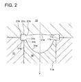
- Fig. 2 is an enlarged view of the mold.
- the mold includes first mold 10, second mold 20 and insert 30 which form a cavity under the condition that they are closed.
- Fig. 1 shows an outline form of the cavity.
- first mold 10 arranged to face second mold 20 includes opening 11a in cylindrical shape, and insert 30 in cylindrical shape is fitted with the inside of opening 11a.
- first optical surface transferring surface 31a for transferring and molding the first optical surface of a lens
- transition surface transferring surface 31b for forming a transition surface, arranged next to the first optical surface transferring surface 31a
- intermediate end surface transferring surface 31c for forming a intermediate end surface, arranged next to transition surface transferring surface 31b
- taper surface 31d arranged next to intermediate end surface transferring surface 31c.
- Intermediate end surface transferring surface 31c is located at a position closest to second mold 20, and is formed so as to be perpendicular to the axis X.
- first optical surface transferring surface 31a there may be formed a fine structure such as ringshaped zones corresponding to a diffractive structure to be formed on a lens.
- first flange end transferring surface 11b On first mold 10, there are formed first flange end transferring surface 11b to be connected to taper surface 31d of insert 30 which is fitted into first mold 10, for transferring and molding the first end surface of a flange section of a lens; and first flange circumference transferring surface 11c which is perpendicular to first flange end transferring surface 11b, for transferring and molding the circumference surface of the flange section.
- First flange end transferring surface 11b is perpendicular to axis X of first optical surface transferring surface 31a (an optical axis of the lens). It is preferable that a chamfer section is arranged on an intersectional position of first flange end transferring surface 11b and first flange circumference transferring surface 11c.
- Second mold 20 includes, around optical axis X as the center, second optical surface transferring surface 21a for transferring and molding the second optical surface of the lens; taper surface 21b arranged next to second optical surface transferring surface 21a; second flange end transferring surface 21c arranged next to taper surface 21b, for transferring and molding the second end surface of the flange section; and second flange circumference transferring surface 21d which is perpendicular to second flange end transferring surface 21c, for transferring and molding the circumference of the flange section.
- Second flange end transferring surface 21c is perpendicular to central axis X of second optical surface transferring surface 21a (the optical axis of the lens). It is preferable that a chamfer section is arranged on an intersectional position of second flange end transferring surface 21c and second flange circumference transferring surface 21d, too.
- gate GT opening channel
- insert 30 is inserted into opening 11a of first mold 10 as shown in Fig. 1a , and first mold 10 is set to face second mold 20.
- first mold 10 and insert 30 are located to approach and come in contact with second mold 20 relatively, and mold closing is carried out with a predetermined pressure kept.
- positions of butting end sections of first flange circumference transferring surface 11c and opposing second flange circumference transferring surface 21d coincide with each other.
- Optical surface transferring surfaces 31a and 21a are heated to a predetermined temperature at the time ofmold closing by heating first mold 10 and second mold 20 by a heater which is not illustrated. After that, resin which is pressurized at an arbitral pressure is supplied through runner 22 and gate GT from a nozzle which is not illustrated (see Fig. 1c ).
- the mold temperature is decreased to cool and solidify the resin.
- first mold 10 and insert 30, and second mold 20 are relatively moved to carry out mold opening, a molded body including lens OE is exposed with sticking to first mold 10.
- lens OE is separated from such the molded body, lens OE as a single body is formed.
- transition surface transferring surface 31b for forming a transition surface is formed between the first optical surface transferring surface 31a and intermediate end surface transferring surface 31c, which can prevent a rapid change of the direction of resin moving toward a cavity in a molding process and allows highly accurate molding with controlling generation of flow marks even when lens OE with large thickness deviation ratio is molded.
- Fig. 3 shows a sectional view of lens OE molded with a mold shown in Figs. 1 and 2 , relating to the present embodiment.
- Fig. 4a is an enlarged view of the section II which is pointed by an arrow in lens OE in Fig. 3
- Fig. 4b is a similar view of lens OE' of a comparative example.
- a lens of the present embodiment will be described, being compared with the comparative example.
- lens OE of the present embodiment includes, around optical axis X as the center, first optical surface (first surface) OE11a formed in spherical shape and including optical axis X; transition surface OE11b formed in ringed shape and arranged next to the first optical surface; intermediate end surface OE 11c formed in ringed shape and arranged next to the transition surface; taper surface OE 11d arranged next to the intermediate end surface; first end surface OE11e of flange section OEF formed in ringed shape and arranged next to the taper surface; and circumference surface OE11f of flange section OEF arranged to be perpendicular to the first end surface.
- a diffractive structure may be arranged on first optical surface OE11a.
- Lens OE includes second optical surface (second surface) OE21a formed in spherical shape and concentrically facing first optical surface OE11a; taper surface OE21b formed in ringed shape and arranged next to the second optical surface; and second end surface OE21c of the flange section arranged next to the taper surface.
- first optical surface OE11a faces a light source and second optical surface OE21a faces an optical disc.
- d axial thickness
- the diameter of an area up to the inner circumference of transition surface OE 11b is represented as D1
- D2 The diameter of an area up to the inner circumference of the intermediate end surface OE11c is represented as D2.
- first optical surface OE11a connects to intermediate end surface OE11c through transition surface OE11b.
- angle ⁇ 1 (which is an acute angle) formed between normal line a and optical axis X is larger than angle ⁇ 2 formed between normal line ⁇ and optical axis X, where normal line a is a normal line of first surface 11a at border B of transition surface OE11b and first surface 11a, and normal line ⁇ is a normal line of transition surface OE11b at border B of first surface OE11a and transition surface OE11b.
- first optical surface OE 11a the angle formed between the normal line of the first optical surface and optical axis X comes closer to 90 degrees gradually, at a position which goes from optical axis X to the radial direction, then, the angle of the normal line becomes shallow when the position goes into transition surface OE11b across border B. Therefore, border B corresponds to an inflection point. Since transition surface OE11b is arranged outside effective aperture E, it does not affect optical properties of lens OE.
- width W of intermediate end surface OE11c in the direction perpendicular to the optical axis is required to be 50 ⁇ m or more for reasons of manufacturing insert 30.
- an objective lens for an optical pickup apparatus it is from about 50 ⁇ m to about 150 ⁇ m generally.
- its minimum thickness t along the optical axis at intermediate end surface OE 11c is larger than the minimum thickness t' of lens OE' of the comparative example along the optical axis at intermediate end surface OE11c, when transition surface OE11b is formed in lens OE, under the assumption that the maximum outer circumferences are uniform.
- the minimum thickness t along the optical axis at intermediate end surface OE11c is smaller than thickness ⁇ of flange section OEF along the optical axis.
- thickness ⁇ of flange section OEF along the optical axis is secured to be large, it has advantages such that, under the condition that lens OE is put on a flat surface, the lens is hardly damaged because of a space formed between second optical surface OE21a and the flat surface.
- border B is arranged at a place that is closer to second optical surface OE21a than first end surface OE11d of flange section OEF and that is closer to first optical surface OE21a than intermediate end surface OE11c.
- the present inventor designed objective lenses with a numerical aperture of 0.85 for an optical pickup apparatus exclusively for a Blu-ray Disc, where the objective lenses have various thickness deviation ratios and various sizes of transition surfaces.
- the present inventor prepared molds (see Fig. 2 ) corresponding to them. After drying resin material at 70°C to 120°C for five hours with hot-air dehumidifying and drying machine to remove water from the material, the inventor conducted injection molding for the material with an injection molding machine "s-2000i 50A" (which is a product name, produced by FANUC CORPORATION) on which a selected mold is attached, at a cylinder temperature of 200°C to 270°C and holding pressure of 70MPa to 100MPa.
- s-2000i 50A which is a product name, produced by FANUC CORPORATION
- the mold temperature was controlled by oil medium. Concretely, a mold cavity temperature in a process of an injection and filling process for resin was set to 120°C to 150°C, and the mold was cooled at the same time when the filling process was completed. After the mold was opened and a lens was taken out from the mold with an automatic taking machine, its degree of appearance defect was evaluated.
- Tables 1 and 2 show the evaluation results.
- the thickness deviation ratio is given by d/t.
- a splitting ratio is given by D1/D2 ⁇ 100.
- the condition that molding defects such as flow marks were caused in 2% or less of samples is represented by the symbol A
- the condition that the mold defects were caused in 2% to 5% of samples is represented by the symbol B
- the condition that the mold defects were caused in 5% to 10% of samples is represented by the symbol C
- the condition that the mold defects were caused in 10% or more of samples is represented by the symbol D.
- the condition that the thickness deviation ratio was 3.3 or more is represented by the symbol A
- the condition that the ratio was 3.3 to 2.8 is represented by the symbol B
- the condition that the ratio was 2.8 to 2.5 is represented by the symbol C
- the condition that the ratio was less than 2.5 is represented by the symbol D.
- the evaluation results in Table 1 show that, when the thickness deviation ratio d/t is 4.1 or less and is 2.8 or more, a molding process can be conducted without problems in actual use. Further, the results show that the thickness deviation ratio d/t in the range of 3.8 or less and 3.3 or more is preferable, for achieving both of proper appearance defects and proper configuration which generally have a trade-off relationship.
- the evaluation results in Table 2 show that, when the split ratio (D1/D2 ⁇ 100) is 88% or more and is 98% or less, a molding process can be conducted without problems. Further, the results show that the split ratio of 94% or more and 97.5% or less is preferable for making the configuration into an excellent condition.
- the present invention has been descried with reference to embodiments. However, it is to be understood that the present invention should not be interpreted under limitations of the above embodiments and various changes and modifications will be apparent to those skilled in the art.
- the present invention can be applied for various lenses not only for an objective lens for use in an optical pickup apparatus.
Landscapes
- Physics & Mathematics (AREA)
- Optics & Photonics (AREA)
- General Physics & Mathematics (AREA)
- Engineering & Computer Science (AREA)
- Health & Medical Sciences (AREA)
- Manufacturing & Machinery (AREA)
- Ophthalmology & Optometry (AREA)
- Mechanical Engineering (AREA)
- Optical Head (AREA)
- Diffracting Gratings Or Hologram Optical Elements (AREA)
- Moulds For Moulding Plastics Or The Like (AREA)
- Lenses (AREA)
Abstract
Description
- The present invention relates to a lens with a NA of 0.7 or more in highly accurate shape.
- In recent years, research and development of a high density optical disc system capable of recording and/or reproducing (hereinafter, "record and/or reproduce" will be referred as "record/reproduce") information by using a blue-violet semiconductor laser with wavelength of about 400 nm are proceeding swiftly. As an example, in the case of an optical disc on which information is recorded/reproduced under the specifications that NA is 0.85 and a light source wavelength is 405 nm, namely, in the case of the so-called Blu-ray Disc (hereinafter, BD), it is possible to record information of 23 to 27 GB per layer for an optical disc with a diameter of 12 cm, which is same in size as DVD (NA is 0.6, wavelength of a light source is 650 nm, and memory capacity is 4.7 GB). This optical disc is referred as a high density optical disc in the present specification.
- As an objective lens for use in an optical pickup apparatus, there is disclosed an objective lens obtained by molding resin, for example, in Patent Literature 1.
-
- Patent Literature 1:
JP-A No. 2003-15031 - As for the lens disclosed in Patent Literature 1, a connecting area is arranged on a portion on a lens surface which is outside from an intersection of the outermost ray within numerical aperture NA and the lens surface, in order to avoid defective molding of a lens. According to a result of study of the present inventor, it has been found that, even when such the connection area is provided, defective molding such as flow marks can be generated under the condition that a thickness deviation ratio (which will be described below) is large. On the other hand, excessively small thickness deviation ratio makes the flange thickness thick, and the effective aperture is hardly enlarged. Accordingly, in a high-NA lens with a large effective aperture, a lens design cannot be achieved in view of optics under the condition that the thickness deviation ratio is small.
- The present invention has been achieved in view of the above problem in the prior art, and is intended to provide a lens which allows to control defects caused in a molding process in a high-NA lens and which is easy to handle.
- A lens described in Claim 1 is a lens which is molded out of a resin material, comprises a flange section on a periphery and has a numerical aperture of 0.7 or more, characterized by comprising:
- a first surface including an optical axis;
- a second surface having a curvature which is smaller than a curvature of the first surface, formed on a side opposite to the first surface;
- an intermediate end surface formed at an area between the first surface and the flange section along a direction perpendicular to the optical axis; and
- a transition surface connecting the intermediate end surface and the first surface,
- wherein an angle θ1 (which is an acute angle) formed between a normal line of the first surface at a border of the transition surface and the first surface and the optical axis, is larger than an angle θ2 formed between a normal line of the transition surface at a border of the first surface and the transition surface and the optical axis, and
- the lens satisfies the following expression, where d (mm) is a distance between the first surface and the second surface on the optical axis and t (mm) is a minimum thicknessalong the optical axis on the intermediate end surface.

- According to the results of the study of the present inventor, it has been found that, though the defective molding can be controlled by arranging the transition surface, the defective molding such as flow marks can be generated even when the transition surface is provided under the condition that d/t (which is referred as a thickness deviation ratio) is 4.1 or more. On the other hand, under the condition that d/t is 2.8 or less, the thickness of a flange becomes excessively thin and the lens is hardly attached to a device with accuracy, for example, when it is an objective lens for an optical pickup apparatus. Therefore, by satisfying the expression (1), a lens with controlled defective molding and excellent property of attachment can be provided.
- A lens descried in Claim 2 is characterized by satisfying the following expression, in the lens of Claim 1. Therefore, a lens with NA of 0.7 or more can be molded while the defective molding is controlled more effectively.

- A lens described in Claim 3 is characterized by satisfying the following expression, in the lens of Claim 1 or 2, where Δ (mm) is a thickness of the flange section along the optical axis.

- For example, in an objective lens for use in a general optical pickup apparatus, a flange section which connects to a connecting area has a uniform thickness. Such the form can control the defective molding with relatively ease, by providing a connecting area. On the other hand, in recent years, a lens achieving both of a thin axial thickness and a thick flange section has been desired. In such the lens, the intermediate end surface is needed to be located closer to the second surface than a surface of the flange section at the first-surface side. Under such the situation, the flow direction of resin which goes to a cavity changes rapidly, which causes defective molding such as flow marks easily. According to that, when the lens is configured such that the thickness deviation ratio d/t satisfies the expression (1), the defective molding can be controlled effectively. In other words, it is especially preferable that the thickness deviation ratio satisfies the expression (1) in a lens satisfying the expression (2).
- A lens described in Claim 4 is characterized by satisfying the following expression, in the lens of any one of Claims 1 to 3, where D1 is a diameter of an area from the optical axis to an inner circumference of the transition surface and D2 is a diameter of an area from the optical axis to an inner circumference of the intermediate end surface.

- When the value of D1/D2 is the upper limit of the expression (3) or more, D1 ∼ D2 holds, which makes a forming process of a mold for molding the above lens difficult. On the other hand, the value of D1/D2 is the lower limit of the expression (3) or less, the transition surface becomes excessively large, which brings decrease of the thickness deviation ratio d/t and is not preferable. Therefore, the condition satisfying the expression (3) is preferable.
- A lens described in Claim 5 is characterized by satisfying the following expression, in the lens of Claim 4.

- A lens described in Claim 6 is characterized in that, in the lens of any one of claims 1 to 5, a width of the intermediate end surface along the direction perpendicular to the optical axis is 50 µm or more. Therefore, it has an advantage that a mold for molding the lens can be easily formed.
- A lens described in Claim 7 is characterized in that, in the lens of any one of Claims 1 to 6, a diffractive structure is formed on at least a part of the first surface. As for a lens having a diffractive structure formed on at least a part of the first surface, its molding is especially difficult. Therefore, in the case that the lens is a lens which has compatibility for three media including a BD and which includes diffractive structures on all the surfaces, its molding process is further more difficult and the effect of the present invention is hoped.
- There is no limitation for resin, as far as it is a transparent thermoplastic resin which is generally used as an optical material. However, in view of workability as an optical element, the followings are preferable: acryl resin, cyclic olefin resin, polycarbonate resin, polyester resin, polyether resin, polyamide resin and polyimide resin. As an applicable thermoplastic resin, for example, there can be cited compositions described in
JP-A No. 2003-73559 - According to the present invention, there can be provided a lens such that defects caused in a molding process can be controlled in a high-NA lens and an excellent attachment property is exhibited.
-
-
Fig. 1 is a diagram showing steps of molding a lens relating to the present embodiment by using a mold. -
Fig. 2 is an enlarged view of the mold. -
Fig. 3 shows lens OE of the present embodiment, molded with a mold. -
Fig. 4a is an enlarged view of a section II pointed by an arrow in lens OE inFig. 3 , andFig. 4b is the similar view of lens OE' of a comparative example. - Embodiments of the present invention will be described below with referring to the drawings.
Fig. 1 is a diagram showing steps of molding a lens with NA of 0.7 or more for use in an optical pickup apparatus for a BD, by using a mold.Fig. 2 is an enlarged view of the mold. The mold includesfirst mold 10,second mold 20 and insert 30 which form a cavity under the condition that they are closed.Fig. 1 shows an outline form of the cavity. - As shown in
Fig. 2 ,first mold 10 arranged to facesecond mold 20 includesopening 11a in cylindrical shape, and insert 30 in cylindrical shape is fitted with the inside ofopening 11a. On the end surface ofinsert 30 which protrudes towardsecond mold 20, there are formed first opticalsurface transferring surface 31a for transferring and molding the first optical surface of a lens; transitionsurface transferring surface 31b for forming a transition surface, arranged next to the first opticalsurface transferring surface 31a; intermediate endsurface transferring surface 31c for forming a intermediate end surface, arranged next to transitionsurface transferring surface 31b; andtaper surface 31d arranged next to intermediate endsurface transferring surface 31c. Intermediate endsurface transferring surface 31c is located at a position closest tosecond mold 20, and is formed so as to be perpendicular to the axis X. On first opticalsurface transferring surface 31a, there may be formed a fine structure such as ringshaped zones corresponding to a diffractive structure to be formed on a lens. - On
first mold 10, there are formed first flangeend transferring surface 11b to be connected to tapersurface 31d ofinsert 30 which is fitted intofirst mold 10, for transferring and molding the first end surface of a flange section of a lens; and first flangecircumference transferring surface 11c which is perpendicular to first flangeend transferring surface 11b, for transferring and molding the circumference surface of the flange section. First flangeend transferring surface 11b is perpendicular to axis X of first opticalsurface transferring surface 31a (an optical axis of the lens). It is preferable that a chamfer section is arranged on an intersectional position of first flangeend transferring surface 11b and first flangecircumference transferring surface 11c. -
Second mold 20 includes, around optical axis X as the center, second opticalsurface transferring surface 21a for transferring and molding the second optical surface of the lens;taper surface 21b arranged next to second opticalsurface transferring surface 21a; second flangeend transferring surface 21c arranged next to tapersurface 21b, for transferring and molding the second end surface of the flange section; and second flangecircumference transferring surface 21d which is perpendicular to second flangeend transferring surface 21c, for transferring and molding the circumference of the flange section. Second flangeend transferring surface 21c is perpendicular to central axis X of second opticalsurface transferring surface 21a (the optical axis of the lens). It is preferable that a chamfer section is arranged on an intersectional position of second flangeend transferring surface 21c and second flangecircumference transferring surface 21d, too. - As shown in
Fig. 1 , gate GT (entrance channel) is formed onfirst mold 10. - Next, a method of molding a lens will be described. At first, insert 30 is inserted into
opening 11a offirst mold 10 as shown inFig. 1a , andfirst mold 10 is set to facesecond mold 20. After that, as shown inFig. 1b ,first mold 10 and insert 30 are located to approach and come in contact withsecond mold 20 relatively, and mold closing is carried out with a predetermined pressure kept. At that time, positions of butting end sections of first flangecircumference transferring surface 11c and opposing second flangecircumference transferring surface 21d coincide with each other. - Optical surface transferring surfaces 31a and 21a are heated to a predetermined temperature at the time ofmold closing by heating
first mold 10 andsecond mold 20 by a heater which is not illustrated. After that, resin which is pressurized at an arbitral pressure is supplied throughrunner 22 and gate GT from a nozzle which is not illustrated (seeFig. 1c ). - Next, after molten resin is solidified with shapes of transferring
surfaces 31a to 31d, 11b to 11c and 21a to 21d being transferred thereon, the mold temperature is decreased to cool and solidify the resin. - After that, when
first mold 10 andinsert 30, andsecond mold 20 are relatively moved to carry out mold opening, a molded body including lens OE is exposed with sticking tofirst mold 10. When lens OE is separated from such the molded body, lens OE as a single body is formed. - According to the present embodiment, transition
surface transferring surface 31b for forming a transition surface is formed between the first opticalsurface transferring surface 31a and intermediate endsurface transferring surface 31c, which can prevent a rapid change of the direction of resin moving toward a cavity in a molding process and allows highly accurate molding with controlling generation of flow marks even when lens OE with large thickness deviation ratio is molded. -
Fig. 3 shows a sectional view of lens OE molded with a mold shown inFigs. 1 and2 , relating to the present embodiment.Fig. 4a is an enlarged view of the section II which is pointed by an arrow in lens OE inFig. 3 , andFig. 4b is a similar view of lens OE' of a comparative example. Hereinafter, a lens of the present embodiment will be described, being compared with the comparative example. - In
Fig. 3 , lens OE of the present embodiment includes, around optical axis X as the center, first optical surface (first surface) OE11a formed in spherical shape and including optical axis X; transition surface OE11b formed in ringed shape and arranged next to the first optical surface; intermediateend surface OE 11c formed in ringed shape and arranged next to the transition surface; taper surface OE 11d arranged next to the intermediate end surface; first end surface OE11e of flange section OEF formed in ringed shape and arranged next to the taper surface; and circumference surface OE11f of flange section OEF arranged to be perpendicular to the first end surface. A diffractive structure may be arranged on first optical surface OE11a. Lens OE includes second optical surface (second surface) OE21a formed in spherical shape and concentrically facing first optical surface OE11a; taper surface OE21b formed in ringed shape and arranged next to the second optical surface; and second end surface OE21c of the flange section arranged next to the taper surface. When the lens is attached to an optical pickup apparatus which is not illustrated, first optical surface OE11a faces a light source and second optical surface OE21a faces an optical disc. Herein, a distance between first optical surface OE11a and second optical surface OE21a along optical axis X is represented as d (axial thickness). The diameter of an area up to the inner circumference oftransition surface OE 11b is represented as D1, and the diameter of an area up to the inner circumference of the intermediate end surface OE11c is represented as D2. - In lens OE' of a comparative example shown in
Fig. 4b , a transition surface does not exist and first optical surface OE11a directly connects to intermediate end surface OE11c. On the other hand, in lens OE of the present embodiment shown inFig. 4a , first optical surface OE11a connects to intermediate end surface OE11c through transition surface OE11b. Herein, angle θ1 (which is an acute angle) formed between normal line a and optical axis X is larger than angle θ2 formed between normal line β and optical axis X, where normal line a is a normal line offirst surface 11a at border B of transition surface OE11b andfirst surface 11a, and normal line β is a normal line of transition surface OE11b at border B of first surface OE11a and transition surface OE11b. In other words, in firstoptical surface OE 11a, the angle formed between the normal line of the first optical surface and optical axis X comes closer to 90 degrees gradually, at a position which goes from optical axis X to the radial direction, then, the angle of the normal line becomes shallow when the position goes into transition surface OE11b across border B. Therefore, border B corresponds to an inflection point. Since transition surface OE11b is arranged outside effective aperture E, it does not affect optical properties of lens OE. - It is generally said that width W of intermediate end surface OE11c in the direction perpendicular to the optical axis is required to be 50 µm or more for reasons of
manufacturing insert 30. As for an objective lens for an optical pickup apparatus, it is from about 50 µm to about 150 µm generally. Accordingly, in lens OE relating to the present embodiment, its minimum thickness t along the optical axis at intermediateend surface OE 11c is larger than the minimum thickness t' of lens OE' of the comparative example along the optical axis at intermediate end surface OE11c, when transition surface OE11b is formed in lens OE, under the assumption that the maximum outer circumferences are uniform. Herein, the minimum thickness t along the optical axis at intermediate end surface OE11c is smaller than thickness Δ of flange section OEF along the optical axis. When thickness Δ of flange section OEF along the optical axis is secured to be large, it has advantages such that, under the condition that lens OE is put on a flat surface, the lens is hardly damaged because of a space formed between second optical surface OE21a and the flat surface. In order to realize a compact lens OE, it is preferable that border B is arranged at a place that is closer to second optical surface OE21a than first end surface OE11d of flange section OEF and that is closer to first optical surface OE21a than intermediate end surface OE11c. - Next, results of experiments which have been conducted by the present inventor will be described. The present inventor designed objective lenses with a numerical aperture of 0.85 for an optical pickup apparatus exclusively for a Blu-ray Disc, where the objective lenses have various thickness deviation ratios and various sizes of transition surfaces. The present inventor prepared molds (see
Fig. 2 ) corresponding to them. After drying resin material at 70°C to 120°C for five hours with hot-air dehumidifying and drying machine to remove water from the material, the inventor conducted injection molding for the material with an injection molding machine "s-2000i 50A" (which is a product name, produced by FANUC CORPORATION) on which a selected mold is attached, at a cylinder temperature of 200°C to 270°C and holding pressure of 70MPa to 100MPa. At that time, the mold temperature was controlled by oil medium. Concretely, a mold cavity temperature in a process of an injection and filling process for resin was set to 120°C to 150°C, and the mold was cooled at the same time when the filling process was completed. After the mold was opened and a lens was taken out from the mold with an automatic taking machine, its degree of appearance defect was evaluated. - Tables 1 and 2 show the evaluation results. In Tables 1 and 2, the thickness deviation ratio is given by d/t. In Table 2, a splitting ratio is given by D1/D2 × 100. In the tables, as for the evaluation of appearance defects, the condition that molding defects such as flow marks were caused in 2% or less of samples is represented by the symbol A, the condition that the mold defects were caused in 2% to 5% of samples is represented by the symbol B, the condition that the mold defects were caused in 5% to 10% of samples is represented by the symbol C, and the condition that the mold defects were caused in 10% or more of samples is represented by the symbol D. As for the evaluation of configuration, the condition that the thickness deviation ratio was 3.3 or more is represented by the symbol A, the condition that the ratio was 3.3 to 2.8 is represented by the symbol B, the condition that the ratio was 2.8 to 2.5 is represented by the symbol C, and the condition that the ratio was less than 2.5 is represented by the symbol D.
Table 1 Thickness deviation ratio Appearance defects Configuration 4.1 C A 3.8 B A 3.5 A A 3.3 A A 2.8 A C 2.5 A C Less than 2.5 A D Table 2 Thickness deviation ratio Split ratio (%) Configuration 4.3 98.5 C 4.06 97.5 A 3.8 96 A 3.3 94.5 A 2.7 90 B 2.5 88 C - The evaluation results in Table 1 show that, when the thickness deviation ratio d/t is 4.1 or less and is 2.8 or more, a molding process can be conducted without problems in actual use. Further, the results show that the thickness deviation ratio d/t in the range of 3.8 or less and 3.3 or more is preferable, for achieving both of proper appearance defects and proper configuration which generally have a trade-off relationship.
- The evaluation results in Table 2 show that, when the split ratio (D1/D2 × 100) is 88% or more and is 98% or less, a molding process can be conducted without problems. Further, the results show that the split ratio of 94% or more and 97.5% or less is preferable for making the configuration into an excellent condition.
- As described above, the present invention has been descried with reference to embodiments. However, it is to be understood that the present invention should not be interpreted under limitations of the above embodiments and various changes and modifications will be apparent to those skilled in the art. For example, the present invention can be applied for various lenses not only for an objective lens for use in an optical pickup apparatus.
-
- 10
- First mold
- 11a
- Optical surface
- 11a
- Opening
- 11b
- Flange end transferring surface
- 11c
- Flange circumference transferring surface
- 20
- Second mold
- 21a
- Optical transferring surface
- 21b
- Taper surface
- 21c
- Flange end transferring surface
- 21d
- Flange circumference transferring surface
- 22
- Runner
- 30
- Insert
- 31a
- Optical surface transferring surface
- 31b
- Transition surface transferring surface
- 31c
- Intermediate end surface transferring surface
- 31d
- Taper surface
- a
- Normal line
- β
- Normal line
- θ1
- Angle
- θ2
- Angle
- B
- Border
- GT
- Gate
- OE
- Lens
- OE11
- Intermediate end surface
- OE11a
- First optical surface
- OE11b
- Transition surface
- OE11c
- Intermediate end surface
- OE11d
- Taper surface
- OE11e
- First end surface of the flange section
- OE11f
- Circumference surface of the flange section
- OE21a
- Second optical surface
- OE21b
- Taper surface
- OE21c
- Second end surface of the flange section
- OEF
- Flange section
- X
- Optical axis or Axis
Claims (7)
- A lens which is molded out of a resin material, comprises a flange section on a periphery and has a numerical aperture of 0.7 or more, characterized by comprising:a first surface including an optical axis;a second surface having a curvature which is smaller than a curvature of the first surface, formed on a side opposite to the first surface;an intermediate end surface formed at an area between the first surface and the flange section along a direction perpendicular to the optical axis; anda transition surface connecting the intermediate end surface and the first surface,wherein an angle θ1 (which is an acute angle) formed between a normal line of the first surface at a border of the transition surface and the first surface and the optical axis, is larger than an angle θ2 formed between a normal line of the transition surface at a border of the first surface and the transition surface and the optical axis, andthe lens satisfies the following expression:

where d (mm) is a distance between the first surface and the second surface on the optical axis and t (mm) is a minimum thickness along the optical axis on the intermediate end surface. - The lens of claim 1, characterized by satisfying the following expression:

- The lens of claim 1 or 2, characterized by satisfying the following expression:

where Δ (mm) is a thickness of the flange section along the optical axis. - The lens of any one of claims 1 to 3, characterized by satisfying the following expression:

where D1 is a diameter of an area from the optical axis to an inner circumference of the transition surface and D2 is a diameter of an area from the optical axis to an inner circumference of the intermediate end surface. - The lens of claim 4, characterized by satisfying the following expression:

- The lens of any one of claims 1 to 5, characterized in that
a width of the intermediate end surface along the direction perpendicular to the optical axis is 50 µm or more. - The lens of any one of claims 1 to 6, characterized in that
a diffractive structure is formed on at least a part of the first surface.
Applications Claiming Priority (2)
| Application Number | Priority Date | Filing Date | Title |
|---|---|---|---|
| JP2009082300 | 2009-03-30 | ||
| PCT/JP2010/052726 WO2010116804A1 (en) | 2009-03-30 | 2010-02-23 | Lens |
Publications (2)
| Publication Number | Publication Date |
|---|---|
| EP2416186A1 true EP2416186A1 (en) | 2012-02-08 |
| EP2416186A4 EP2416186A4 (en) | 2012-09-19 |
Family
ID=42936092
Family Applications (1)
| Application Number | Title | Priority Date | Filing Date |
|---|---|---|---|
| EP10761506A Withdrawn EP2416186A4 (en) | 2009-03-30 | 2010-02-23 | Lens |
Country Status (6)
| Country | Link |
|---|---|
| US (1) | US20120019912A1 (en) |
| EP (1) | EP2416186A4 (en) |
| JP (2) | JP4993326B2 (en) |
| KR (1) | KR20110131233A (en) |
| CN (1) | CN102365563B (en) |
| WO (1) | WO2010116804A1 (en) |
Families Citing this family (7)
| Publication number | Priority date | Publication date | Assignee | Title |
|---|---|---|---|---|
| JP5716754B2 (en) * | 2011-02-04 | 2015-05-13 | コニカミノルタ株式会社 | Objective lens manufacturing method and mold |
| JP5716755B2 (en) * | 2011-02-04 | 2015-05-13 | コニカミノルタ株式会社 | Objective lens manufacturing method and mold |
| WO2012111748A1 (en) * | 2011-02-16 | 2012-08-23 | コニカミノルタオプト株式会社 | Method for manufacturing optical element, and optical element |
| JP5733388B2 (en) * | 2011-03-28 | 2015-06-10 | コニカミノルタ株式会社 | Objective lens, objective lens manufacturing method, and molding die |
| WO2016136089A1 (en) * | 2015-02-27 | 2016-09-01 | 富士フイルム株式会社 | Solid electrolyte composition, battery electrode sheet and manufacturing method thereof, and all-solid-state secondary battery and manufacturing method thereof |
| JP7195058B2 (en) * | 2017-03-31 | 2022-12-23 | 三井化学株式会社 | Cyclic olefin resin composition, molded article and optical part |
| JP7438811B2 (en) * | 2020-03-26 | 2024-02-27 | キヤノン株式会社 | Optical system and image display device |
Family Cites Families (13)
| Publication number | Priority date | Publication date | Assignee | Title |
|---|---|---|---|---|
| TW504582B (en) * | 1999-09-01 | 2002-10-01 | Konishiroku Photo Ind | Objective lens for pickup and light pickup apparatus |
| JP4737480B2 (en) * | 2000-12-28 | 2011-08-03 | コニカミノルタホールディングス株式会社 | Optical element manufacturing method |
| JP2002200654A (en) * | 2000-12-28 | 2002-07-16 | Konica Corp | Method for manufacturing optical element, and optical element |
| JP4232188B2 (en) | 2001-04-26 | 2009-03-04 | コニカミノルタホールディングス株式会社 | Objective lens for optical pickup device, optical pickup device and optical information recording / reproducing device |
| JP4485717B2 (en) | 2001-09-04 | 2010-06-23 | 三井化学株式会社 | Thermoplastic material composition and optical component comprising the same |
| JP2003248106A (en) * | 2002-02-25 | 2003-09-05 | Mitsubishi Electric Corp | Optical element |
| US7426078B2 (en) * | 2002-11-26 | 2008-09-16 | Hitachi Maxell, Ltd. | Plastic lens, manufacturing method thereof, production tracing management method thereof, and optical pickup device |
| JP4321078B2 (en) * | 2003-02-28 | 2009-08-26 | コニカミノルタホールディングス株式会社 | Molded lens |
| JP4258353B2 (en) * | 2003-10-31 | 2009-04-30 | コニカミノルタオプト株式会社 | Optical element |
| TWI353463B (en) * | 2004-02-27 | 2011-12-01 | Konica Minolta Opto Inc | Optical element and manufacturing method of the op |
| WO2008053692A1 (en) * | 2006-11-01 | 2008-05-08 | Konica Minolta Opto, Inc. | Optical element, resin molding metal die and optical element manufacturing method |
| JPWO2008117587A1 (en) * | 2007-03-28 | 2010-07-15 | コニカミノルタオプト株式会社 | Optical element for optical pickup device and optical pickup device |
| JP2009123316A (en) * | 2007-11-19 | 2009-06-04 | Fujinon Corp | Objective lens, optical pickup device provided with the same, and optical recording medium recording and/or playback device mounting this optical pickup device |
-
2010
- 2010-02-23 EP EP10761506A patent/EP2416186A4/en not_active Withdrawn
- 2010-02-23 US US13/260,725 patent/US20120019912A1/en not_active Abandoned
- 2010-02-23 JP JP2011508273A patent/JP4993326B2/en active Active
- 2010-02-23 KR KR1020117022473A patent/KR20110131233A/en not_active Withdrawn
- 2010-02-23 WO PCT/JP2010/052726 patent/WO2010116804A1/en not_active Ceased
- 2010-02-23 CN CN201180001577.9A patent/CN102365563B/en not_active Expired - Fee Related
-
2012
- 2012-04-19 JP JP2012095269A patent/JP2012190533A/en not_active Withdrawn
Also Published As
| Publication number | Publication date |
|---|---|
| JP2012190533A (en) | 2012-10-04 |
| KR20110131233A (en) | 2011-12-06 |
| US20120019912A1 (en) | 2012-01-26 |
| JPWO2010116804A1 (en) | 2012-10-18 |
| JP4993326B2 (en) | 2012-08-08 |
| CN102365563B (en) | 2014-03-12 |
| CN102365563A (en) | 2012-02-29 |
| WO2010116804A1 (en) | 2010-10-14 |
| EP2416186A4 (en) | 2012-09-19 |
Similar Documents
| Publication | Publication Date | Title |
|---|---|---|
| EP2416186A1 (en) | Lens | |
| EP2385397A1 (en) | Lens and molding die | |
| US7365919B2 (en) | Forming methods, forming devices for articles having a micro-sized shape and optical elements | |
| JP4855530B2 (en) | Plastic lens and optical pickup device | |
| JP4407148B2 (en) | Optical element manufacturing method and apparatus, and optical element | |
| CN103370182A (en) | Method for manufacturing optical element, and optical element | |
| US6881051B2 (en) | Mold for injection molding of disc substrate | |
| US20120182625A1 (en) | Optical Element | |
| US20120182855A1 (en) | Objective Lens and Optical Pickup Device | |
| JP2004191948A5 (en) | ||
| JP2004191948A (en) | Plastic lens and optical pickup device | |
| JP2004188972A (en) | Plastic lens, manufacturing method thereof, history management method of plastic lens, and optical pickup device | |
| JP4808089B2 (en) | Optical element molding method | |
| JP2005049829A (en) | Molding having minute shape, optical element, molding method and molding apparatus | |
| JP2006327147A (en) | Forming method of plastic lens and plastic lens | |
| JP2002221604A (en) | Optical element and optical pickup device | |
| JP2007147888A (en) | Plastic lens and optical pickup device | |
| JP2011118964A (en) | Objective lens and molding die for optical pickup device | |
| WO2011093165A1 (en) | Objective lens and optical pickup device | |
| CN103959381A (en) | Optical element and production method therefor | |
| JP2002260299A (en) | Optical disk substrate molding method and apparatus, stamper, optical disk substrate molding die, and optical disk | |
| JP2000222779A (en) | Optical disc and method of manufacturing the same | |
| JPH1086190A (en) | Optical disk substrate molding die and stamper mounting method | |
| JP2008062577A (en) | Mold for molding optical disk substrate and molding method | |
| JP2002260298A (en) | Mold for manufacturing optical disk substrates |
Legal Events
| Date | Code | Title | Description |
|---|---|---|---|
| PUAI | Public reference made under article 153(3) epc to a published international application that has entered the european phase |
Free format text: ORIGINAL CODE: 0009012 |
|
| 17P | Request for examination filed |
Effective date: 20110926 |
|
| AK | Designated contracting states |
Kind code of ref document: A1 Designated state(s): AT BE BG CH CY CZ DE DK EE ES FI FR GB GR HR HU IE IS IT LI LT LU LV MC MK MT NL NO PL PT RO SE SI SK SM TR |
|
| DAX | Request for extension of the european patent (deleted) | ||
| A4 | Supplementary search report drawn up and despatched |
Effective date: 20120821 |
|
| RIC1 | Information provided on ipc code assigned before grant |
Ipc: B29D 11/00 20060101ALI20120815BHEP Ipc: G02B 7/02 20060101ALI20120815BHEP Ipc: G11B 7/135 20120101ALI20120815BHEP Ipc: G02B 5/18 20060101ALN20120815BHEP Ipc: G02B 3/00 20060101AFI20120815BHEP |
|
| RIC1 | Information provided on ipc code assigned before grant |
Ipc: G11B 7/135 20120101ALI20130314BHEP Ipc: G02B 7/02 20060101ALI20130314BHEP Ipc: B29D 11/00 20060101ALI20130314BHEP Ipc: G02B 3/00 20060101AFI20130314BHEP Ipc: G02B 5/18 20060101ALN20130314BHEP Ipc: G11B 7/1374 20120101ALI20130314BHEP |
|
| STAA | Information on the status of an ep patent application or granted ep patent |
Free format text: STATUS: THE APPLICATION HAS BEEN WITHDRAWN |
|
| 18W | Application withdrawn |
Effective date: 20130916 |