EP2410826A1 - Flexible printed circuit board with waterproof structure - Google Patents
Flexible printed circuit board with waterproof structure Download PDFInfo
- Publication number
- EP2410826A1 EP2410826A1 EP11005929A EP11005929A EP2410826A1 EP 2410826 A1 EP2410826 A1 EP 2410826A1 EP 11005929 A EP11005929 A EP 11005929A EP 11005929 A EP11005929 A EP 11005929A EP 2410826 A1 EP2410826 A1 EP 2410826A1
- Authority
- EP
- European Patent Office
- Prior art keywords
- metal layer
- circuit board
- printed circuit
- flexible printed
- resistant member
- Prior art date
- Legal status (The legal status is an assumption and is not a legal conclusion. Google has not performed a legal analysis and makes no representation as to the accuracy of the status listed.)
- Granted
Links
- 229910052751 metal Inorganic materials 0.000 claims abstract description 76
- 239000002184 metal Substances 0.000 claims abstract description 76
- XLYOFNOQVPJJNP-UHFFFAOYSA-N water Substances O XLYOFNOQVPJJNP-UHFFFAOYSA-N 0.000 claims abstract description 68
- 238000009413 insulation Methods 0.000 claims abstract description 23
- 239000000758 substrate Substances 0.000 claims abstract description 18
- 239000000463 material Substances 0.000 claims description 16
- BQCADISMDOOEFD-UHFFFAOYSA-N Silver Chemical compound [Ag] BQCADISMDOOEFD-UHFFFAOYSA-N 0.000 claims description 11
- 230000002708 enhancing effect Effects 0.000 claims description 11
- 239000002245 particle Substances 0.000 claims description 9
- RYGMFSIKBFXOCR-UHFFFAOYSA-N Copper Chemical compound [Cu] RYGMFSIKBFXOCR-UHFFFAOYSA-N 0.000 claims description 8
- 229910052802 copper Inorganic materials 0.000 claims description 8
- 239000010949 copper Substances 0.000 claims description 8
- 229920001971 elastomer Polymers 0.000 claims description 7
- 239000005060 rubber Substances 0.000 claims description 7
- 229910052709 silver Inorganic materials 0.000 claims description 7
- 239000004332 silver Substances 0.000 claims description 7
- VYPSYNLAJGMNEJ-UHFFFAOYSA-N Silicium dioxide Chemical compound O=[Si]=O VYPSYNLAJGMNEJ-UHFFFAOYSA-N 0.000 claims description 6
- 239000011248 coating agent Substances 0.000 claims description 6
- 238000000576 coating method Methods 0.000 claims description 6
- 239000000741 silica gel Substances 0.000 claims description 6
- 229910002027 silica gel Inorganic materials 0.000 claims description 6
- 229920002379 silicone rubber Polymers 0.000 claims description 6
- 239000004945 silicone rubber Substances 0.000 claims description 6
- 229910052782 aluminium Inorganic materials 0.000 claims description 4
- XAGFODPZIPBFFR-UHFFFAOYSA-N aluminium Chemical compound [Al] XAGFODPZIPBFFR-UHFFFAOYSA-N 0.000 claims description 4
- 239000011888 foil Substances 0.000 claims description 4
- 239000011347 resin Substances 0.000 claims description 3
- 229920005989 resin Polymers 0.000 claims description 3
- 239000010410 layer Substances 0.000 description 61
- 238000004078 waterproofing Methods 0.000 description 10
- 230000000694 effects Effects 0.000 description 4
- 230000005540 biological transmission Effects 0.000 description 3
- PXHVJJICTQNCMI-UHFFFAOYSA-N Nickel Chemical compound [Ni] PXHVJJICTQNCMI-UHFFFAOYSA-N 0.000 description 2
- 239000004020 conductor Substances 0.000 description 2
- 238000000034 method Methods 0.000 description 2
- 230000008054 signal transmission Effects 0.000 description 2
- 238000005476 soldering Methods 0.000 description 2
- OKTJSMMVPCPJKN-UHFFFAOYSA-N Carbon Chemical compound [C] OKTJSMMVPCPJKN-UHFFFAOYSA-N 0.000 description 1
- ATJFFYVFTNAWJD-UHFFFAOYSA-N Tin Chemical compound [Sn] ATJFFYVFTNAWJD-UHFFFAOYSA-N 0.000 description 1
- 239000003795 chemical substances by application Substances 0.000 description 1
- 230000008878 coupling Effects 0.000 description 1
- 238000010168 coupling process Methods 0.000 description 1
- 238000005859 coupling reaction Methods 0.000 description 1
- 238000005530 etching Methods 0.000 description 1
- PCHJSUWPFVWCPO-UHFFFAOYSA-N gold Chemical compound [Au] PCHJSUWPFVWCPO-UHFFFAOYSA-N 0.000 description 1
- 229910052737 gold Inorganic materials 0.000 description 1
- 239000010931 gold Substances 0.000 description 1
- 229910002804 graphite Inorganic materials 0.000 description 1
- 239000010439 graphite Substances 0.000 description 1
- 239000012774 insulation material Substances 0.000 description 1
- 230000009545 invasion Effects 0.000 description 1
- 238000004519 manufacturing process Methods 0.000 description 1
- 238000012986 modification Methods 0.000 description 1
- 230000004048 modification Effects 0.000 description 1
- 229910052759 nickel Inorganic materials 0.000 description 1
- 238000007789 sealing Methods 0.000 description 1
- 238000000926 separation method Methods 0.000 description 1
- 239000002344 surface layer Substances 0.000 description 1
Images


Classifications
-
- H—ELECTRICITY
- H05—ELECTRIC TECHNIQUES NOT OTHERWISE PROVIDED FOR
- H05K—PRINTED CIRCUITS; CASINGS OR CONSTRUCTIONAL DETAILS OF ELECTRIC APPARATUS; MANUFACTURE OF ASSEMBLAGES OF ELECTRICAL COMPONENTS
- H05K1/00—Printed circuits
- H05K1/02—Details
- H05K1/0213—Electrical arrangements not otherwise provided for
- H05K1/0237—High frequency adaptations
- H05K1/025—Impedance arrangements, e.g. impedance matching, reduction of parasitic impedance
- H05K1/0253—Impedance adaptations of transmission lines by special lay-out of power planes, e.g. providing openings
-
- H—ELECTRICITY
- H05—ELECTRIC TECHNIQUES NOT OTHERWISE PROVIDED FOR
- H05K—PRINTED CIRCUITS; CASINGS OR CONSTRUCTIONAL DETAILS OF ELECTRIC APPARATUS; MANUFACTURE OF ASSEMBLAGES OF ELECTRICAL COMPONENTS
- H05K3/00—Apparatus or processes for manufacturing printed circuits
- H05K3/22—Secondary treatment of printed circuits
- H05K3/28—Applying non-metallic protective coatings
-
- H—ELECTRICITY
- H05—ELECTRIC TECHNIQUES NOT OTHERWISE PROVIDED FOR
- H05K—PRINTED CIRCUITS; CASINGS OR CONSTRUCTIONAL DETAILS OF ELECTRIC APPARATUS; MANUFACTURE OF ASSEMBLAGES OF ELECTRICAL COMPONENTS
- H05K1/00—Printed circuits
- H05K1/02—Details
-
- H—ELECTRICITY
- H05—ELECTRIC TECHNIQUES NOT OTHERWISE PROVIDED FOR
- H05K—PRINTED CIRCUITS; CASINGS OR CONSTRUCTIONAL DETAILS OF ELECTRIC APPARATUS; MANUFACTURE OF ASSEMBLAGES OF ELECTRICAL COMPONENTS
- H05K5/00—Casings, cabinets or drawers for electric apparatus
- H05K5/06—Hermetically-sealed casings
- H05K5/069—Other details of the casing, e.g. wall structure, passage for a connector, a cable, a shaft
-
- H—ELECTRICITY
- H05—ELECTRIC TECHNIQUES NOT OTHERWISE PROVIDED FOR
- H05K—PRINTED CIRCUITS; CASINGS OR CONSTRUCTIONAL DETAILS OF ELECTRIC APPARATUS; MANUFACTURE OF ASSEMBLAGES OF ELECTRICAL COMPONENTS
- H05K2201/00—Indexing scheme relating to printed circuits covered by H05K1/00
- H05K2201/01—Dielectrics
- H05K2201/0104—Properties and characteristics in general
- H05K2201/0133—Elastomeric or compliant polymer
-
- H—ELECTRICITY
- H05—ELECTRIC TECHNIQUES NOT OTHERWISE PROVIDED FOR
- H05K—PRINTED CIRCUITS; CASINGS OR CONSTRUCTIONAL DETAILS OF ELECTRIC APPARATUS; MANUFACTURE OF ASSEMBLAGES OF ELECTRICAL COMPONENTS
- H05K2203/00—Indexing scheme relating to apparatus or processes for manufacturing printed circuits covered by H05K3/00
- H05K2203/11—Treatments characterised by their effect, e.g. heating, cooling, roughening
- H05K2203/1147—Sealing or impregnating, e.g. of pores
Definitions
- the present invention relates to a flexible printed circuit board with waterproof structure, and in particular to a flexible printed circuit board having a metal layer, which carries an insulation layer formed thereon and forms a mounting zone that is not covered by the insulation and is thus exposed for receiving a water resistant member mounted thereon, wherein the mounting zone comprises a bonding strength enhancing structure to improve the bonding strength of the water resistant member to the flexible printed circuit board, and the metal layer forms holes through a surface thereof to improve control over impedance against high frequency signals.
- a conventional flexible printed circuit board is composed of a plurality of conductors that are respectively covered by an insulation jacket and are arranged to juxtapose each other to form a flat structure.
- the flexible printed circuit board can be connected through electrical connectors or soldering for transmission of electronic signals.
- Connecting electronic devices with a flexible printed circuit board is generally of no concern of waterproofing.
- waterproofing may become a problem especially for outdoor applications or for portable devices, such as mobile phones.
- the mobile phone comprises a host device portion and a display screen portion that are connected to each other by a flexible printed circuit board that is attached to these portions through connectors or soldering. If waterproofing between the flexible printed circuit board and the host device portion or the display screen portion of the mobile phone is poor, then water may flow along the flexible printed circuit board into the host device portion and the display screen portion.
- a rubber pad is provided as a waterproof or water-resistant member arranged between an enclosure of an electronic device and a flexible printed circuit board, whereby tight engagement is established between the flexible printed circuit board and the electronic device enclosure to achieve the desired effect of waterproofing or resistance against humidity.
- an objective of the present invention is to provide a flexible printed circuit board with waterproof structure, which comprises a flexible substrate carrying a metal layer on which an insulation layer is formed.
- the metal layer forms a mounting zone that is not covered by the insulation layer and is thus exposed.
- the metal layer forms holes or corrugation on a surface thereon within the mounting zone in order to improve the bonding strength.
- a water resistant member is mounted to the mounting zone of the metal layer so that excellent waterproofing and bonding can be realized between the water resistant member and the flexible printed circuit board.
- Another objective of the present invention is to provide a water-resistant flexible printed circuit board that features both the waterproofing and bonding between a water resistant member and the flexible printed circuit board and the requirement of impedance for the flexible printed circuit board.
- a water resistant member mounted to the flexible printed circuit board being fit to a receptacle opening defined in a device enclosure, excellent bonding strength is realized between the water resistant member and the flexible printed circuit board and the requirement for controlling impedance of a high frequency flexible printed circuit board can also be achieved.
- a flexible substrate has a first surface on which a first metal layer is bonded.
- the first metal layer has an upper surface forming a covered area and at least one mounting zone.
- a first insulation layer is formed on the covered area of the upper surface of the first metal layer in such a way not to cover the mounting zone of the first metal so as to expose the mounting zone.
- a water resistant member is securely mounted to the mounting zone of the first metal layer.
- the flexible substrate also has a second surface to which a second metal layer and a second insulation layer are selectively and sequentially mounted.
- the second metal layer also forms a mounting zone, which is not covered by the second insulation layer so as to expose for mounting the water resistant member.
- the water resistant member mounting zone of each metal layer is provided with a bonding strength enhancing structure for securely bonding the water resistant member.
- the bonding strength enhancing structure comprises at least one hole extending through the upper and lower surfaces of the metal layer or a corrugation structure that does not extend through the upper and lower surfaces of the metal layer.
- the hole of the bonding strength enhancing structure can be of a shape of circle, square or rectangle, rhombus, ellipse, or triangle. In a preferred embodiment, the hole is of a size that is greater than 0,001 inches. For multiple holes, it is preferable that the holes are distributed uniformly.
- the holes can be formed through conventional development/etching processes, or printing of silver paste, or bonding of pre-formed holed structure, or secondary printing of holed silver paste layer on a surface of the metal layer to form corrugation.
- the process is selected according to the material of the layer and the size and distribution density of the holes.
- the metal layer is made of a material of copper, copper with metallic surface coating, silver paste, silver foil, and aluminum foil.
- the water resistant member can be made of a material showing insulating characteristics, or a material showing electrical conduction characteristics. According to the needs of various applications, the material selected helps realizing the effect of insulation, electrical conductivity, or magnetic shielding.
- the water resistant member is made of an electrically conductive material, the water resistant member serves to connect the metallic shielding layer of a flexible printed circuit board with a metallic casing to provide improved electromagnetic shielding effect.
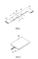
- FIG 1 is a perspective view showing a flexible printed circuit board with water-resistant structure according to a first embodiment of the present invention
- FIG 2 is a perspective view showing the present invention coupled to a receptacle opening formed in a device enclosure through a water resistant member;
- FIG. 3 is a perspective view showing the flexible printed circuit board according to the present invention with the water resistant member removed;
- FIG. 4 is a cross-sectional, in an exploded form, of the flexible printed circuit board according to the present invention.
- FIG. 5 is a cross-sectional view taken along line 5-5 of FIG 1 ;
- FIG 6 is a cross-sectional view taken along line 6-6 of FIG. 1 ;
- FIG 7 is a cross-sectional view, in an exploded form, showing a metal layer comprising a corrugation structure formed on a surface thereof;
- FIG 8 is a cross-sectional view showing a flexible printed circuit board with water-resistant structure according to a second embodiment of the present invention.
- FIG 9 is a cross-sectional view showing a flexible printed circuit board with water-resistant structure according to a third embodiment of the present invention.
- FIG. 1 shows a perspective view of a flexible printed circuit board with water-resistant structure according to a first embodiment of the present invention, which is generally designated at 100 .
- the flexible printed circuit board 100 of the present invention upon coupling to a device enclosure 200 (as shown in FIG. 2 ), inserts a water resistant member 300 into a receptacle opening defined in the device enclosure 200 to protect the device enclosure 200 , which may be an enclosure of an electronic device, from water ingress or invasion.
- the flexible printed circuit board 100 is of wide application for use in the enclosure of various electronic devices.
- the flexible printed circuit board 100 when used in the field of mobile phones, can be attached to a host device portion and a display screen portion through connectors 101, 102 attached thereto.
- the flexible printed circuit board 100 may be replaced with another type of flexible circuit board or cable, such as a well-known flexible flat cable.
- FIG. 3 shows a perspective view of the flexible printed circuit board 100 according to the present invention with the water resistant member 300 removed.
- FIG. 4 shows a cross-sectional view, in an exploded form, of the flexible printed circuit board 100 according to the present invention.
- FIG. 5 shows a cross-sectional view taken along line 5-5 of FIG 1 .
- FIG. 6 shows a cross-sectional view taken along line 6-6 of FIG 1 .
- a flexible substrate 1 has a first surface 11 on which a first metal layer 2 is formed.
- the first metal layer 2 has an upper surface 21 on which a covered area 211 and at least one water resistant member mounting zone 212 are defined.
- the first metal layer 2 has an opposite lower surface 22 bonded to the first surface 11 of the flexible substrate 1 .
- the first metal layer 2 may serve as an electromagnetic shielding layer for the flexible substrate 1 and can be made of a material of one of copper, copper with metallic surface coating (such as tin coating and gold coating), silver paste, silver foil, and aluminum foil.
- a first insulation layer 3 is formed on the covered area 211 of the upper surface 21 of the first metal layer 2 in such a way that the water resistant member mounting zone 212 of the first metal layer 2 is not covered and is thus exposed.
- the flexible substrate 1 has an opposite second surface 12 on which a second metal layer 2a is formed.
- the second metal layer 2a has a lower surface to which a second insulation layer 3a is attached.
- the lower surface of the second metal layer 2a also forms a covered area 211a and at least one water resistant member mounting zone 212a.
- a water resistant member 300 is tightly mounted to the water resistant member mounting zone 212 of the first metal layer 2, the water resistant member mounting zone 212a of the second metal layer 2a, and circumferential portions of the flexible substrate 1.
- the water resistant member 300 is made of a material showing insulating characteristics, such as silicone rubber, rubber, silica gel, whereby excellent insulation can be achieved through the use of these materials.
- the water resistant member 300 may alternatively made of a material showing electrical conductivity, such as silicone rubber, rubber, silica gel, or resin, that contains therein electrically conductive particles (such as graphite, silver, nickel), whereby electrical conductivity and magnetic shielding can be achieved through the use of these materials.
- the water resistant member 300 besides covering the water resistant member mounting zone 212, 212a, additionally covers an interface area between the water resistant member mounting zone 212 and the first insulation layer 3 and an interface area between the water resistant member mounting zone 212a and the second insulation layer 3a.
- the first metal layer 2 forms at least one hole 213 (multiple holes being shown in the embodiment illustrated) extending completely through the upper surface 21 and the lower surface 22 of the first metal layer 2 so as to form a hollow opening pattern in the water resistant member mounting zone 212.
- the arrangement of the hollow opening pattern helps controlling the impedance and transmission time of the first metal layer 2.
- the holes 213 are circular in the embodiment illustrated, but can be of other shapes, such as rhombus, square or rectangle, ellipse, triangle, or other suitable geometric configuration.
- the hollow opening pattern formed in the water resistant member mounting zone 212 of the first metal layer 2 is also helpful in improving the bonding strength between the water resistant member mounting zone 212 of the first metal layer 2 and the water resistant member 300.
- the water resistant member mounting zone of the first metal layer may alternatively and/or additionally form a corrugation structure 214 (as shown in FIG 7 ) that does not extend through the lower surface and the upper surface of the first metal layer.
- the corrugation structure 214 help improving the bonding strength between the water resistant member mounting zone 212 of the first metal layer 2 and the water resistant member 300.
- the corrugation structure 214 can be formed of patterns of circle, rhombus, square or rectangle, ellipse, triangle, or other suitable geometric configurations.
- a double-sided flexible printed circuit board is taken as an example of illustration, yet the present invention is also applicable to single-sided or multi-layered flexible printed circuit board.
- a flexible substrate 1 has a first surface 11 on which a first metal layer 2 is formed; a first insulation layer 3 is further formed on an upper surface 21 of the first metal layer 2 within a covered area 211; and a water resistant member 300 is securely mounted around an interface area between the water resistant member mounting zone 212 of the first metal layer 2 and the flexible substrate 1 .
- the instant embodiment comprises a flexible substrate 1 having a second surface 12 that comprises no second metal layer 2a and second insulation layer 3a.
- water resistant member 300 besides being configured as a regular rectangular form, may be alternatively configured in other geometric forms, such as a rounded water resistant member 300a (shown in FIG. 9 ), in order to meet the needs of various device enclosures.
Landscapes
- Engineering & Computer Science (AREA)
- Microelectronics & Electronic Packaging (AREA)
- Manufacturing & Machinery (AREA)
- Structure Of Printed Boards (AREA)
- Insulated Conductors (AREA)
- Installation Of Indoor Wiring (AREA)
- Shielding Devices Or Components To Electric Or Magnetic Fields (AREA)
- Insertion, Bundling And Securing Of Wires For Electric Apparatuses (AREA)
Abstract
Description
- The present invention relates to a flexible printed circuit board with waterproof structure, and in particular to a flexible printed circuit board having a metal layer, which carries an insulation layer formed thereon and forms a mounting zone that is not covered by the insulation and is thus exposed for receiving a water resistant member mounted thereon, wherein the mounting zone comprises a bonding strength enhancing structure to improve the bonding strength of the water resistant member to the flexible printed circuit board, and the metal layer forms holes through a surface thereof to improve control over impedance against high frequency signals.
- Flexible printed circuit boards are of wide applications in various electronic devices, such as notebook computers, personal digital assistants, and mobile phones. A conventional flexible printed circuit board is composed of a plurality of conductors that are respectively covered by an insulation jacket and are arranged to juxtapose each other to form a flat structure. The flexible printed circuit board can be connected through electrical connectors or soldering for transmission of electronic signals.
- Connecting electronic devices with a flexible printed circuit board is generally of no concern of waterproofing. However, waterproofing may become a problem especially for outdoor applications or for portable devices, such as mobile phones. Taking a mobile phone as an example, the mobile phone comprises a host device portion and a display screen portion that are connected to each other by a flexible printed circuit board that is attached to these portions through connectors or soldering. If waterproofing between the flexible printed circuit board and the host device portion or the display screen portion of the mobile phone is poor, then water may flow along the flexible printed circuit board into the host device portion and the display screen portion.
- To effect waterproofing or resistance against humidity, conventionally, a rubber pad is provided as a waterproof or water-resistant member arranged between an enclosure of an electronic device and a flexible printed circuit board, whereby tight engagement is established between the flexible printed circuit board and the electronic device enclosure to achieve the desired effect of waterproofing or resistance against humidity.
- Although directly mounting a water resistant member on an insulation surface layer of a flexible printed circuit board is known and is also effective in achieving waterproofing or resistance against humidity. However, there is still a concern about reliability of water sealing between the water resistant member and the printed circuit board. One of the reasons is that it is hard to properly establish a tight engagement between the water resistant member and the surface insulation material (such as PI and insulation ink) of the printed circuit board. Although surface treating agents may be applied to handle this problem, the resultant waterproofing and bonding strength are not good enough so that any flaw occurring in the manufacturing process will lead to unacceptable bonding strength between the water resistant member and the printed circuit board, causing undesired situations of shifting, separation, leaking of water between the water resistant member and the printed circuit board , which eventually result in poor resistance against water pressures applied thereto.
- Further, when a flexible printed circuit board is employed to transmit electronic signals of high frequency, there is always a concern about impedance matching and control of signal transmission time. Since a flexible printed circuit board is of a reduced thickness, the distance between two surface metallic shielding layers and the signals transmitted is very small, leading to excessively low impedance to the signal transmission. A solution to such a problem is to form openings in local area or the whole area of the metallic shielding layers, which always lead to the desired result of impedance. It is thus of a desire to combine a structure for effecting waterproofing and bonding between the water resistant member and the flexible printed circuit board and a structure for controlling high frequency impedance of the flexible printed circuit board, in order to improve the industrial value of a flexible printed circuit board.
- Thus, an objective of the present invention is to provide a flexible printed circuit board with waterproof structure, which comprises a flexible substrate carrying a metal layer on which an insulation layer is formed. The metal layer forms a mounting zone that is not covered by the insulation layer and is thus exposed. The metal layer forms holes or corrugation on a surface thereon within the mounting zone in order to improve the bonding strength. A water resistant member is mounted to the mounting zone of the metal layer so that excellent waterproofing and bonding can be realized between the water resistant member and the flexible printed circuit board.
- Another objective of the present invention is to provide a water-resistant flexible printed circuit board that features both the waterproofing and bonding between a water resistant member and the flexible printed circuit board and the requirement of impedance for the flexible printed circuit board. With a water resistant member mounted to the flexible printed circuit board being fit to a receptacle opening defined in a device enclosure, excellent bonding strength is realized between the water resistant member and the flexible printed circuit board and the requirement for controlling impedance of a high frequency flexible printed circuit board can also be achieved.
- To achieve the above objective, a flexible substrate has a first surface on which a first metal layer is bonded. The first metal layer has an upper surface forming a covered area and at least one mounting zone. A first insulation layer is formed on the covered area of the upper surface of the first metal layer in such a way not to cover the mounting zone of the first metal so as to expose the mounting zone. A water resistant member is securely mounted to the mounting zone of the first metal layer. The flexible substrate also has a second surface to which a second metal layer and a second insulation layer are selectively and sequentially mounted. The second metal layer also forms a mounting zone, which is not covered by the second insulation layer so as to expose for mounting the water resistant member. In the embodiments of the present invention, the water resistant member mounting zone of each metal layer is provided with a bonding strength enhancing structure for securely bonding the water resistant member. The bonding strength enhancing structure comprises at least one hole extending through the upper and lower surfaces of the metal layer or a corrugation structure that does not extend through the upper and lower surfaces of the metal layer. The hole of the bonding strength enhancing structure can be of a shape of circle, square or rectangle, rhombus, ellipse, or triangle. In a preferred embodiment, the hole is of a size that is greater than 0,001 inches. For multiple holes, it is preferable that the holes are distributed uniformly. The holes can be formed through conventional development/etching processes, or printing of silver paste, or bonding of pre-formed holed structure, or secondary printing of holed silver paste layer on a surface of the metal layer to form corrugation. The process is selected according to the material of the layer and the size and distribution density of the holes. The metal layer is made of a material of copper, copper with metallic surface coating, silver paste, silver foil, and aluminum foil.
- The water resistant member can be made of a material showing insulating characteristics, or a material showing electrical conduction characteristics. According to the needs of various applications, the material selected helps realizing the effect of insulation, electrical conductivity, or magnetic shielding. When the water resistant member is made of an electrically conductive material, the water resistant member serves to connect the metallic shielding layer of a flexible printed circuit board with a metallic casing to provide improved electromagnetic shielding effect.
- The present invention will be apparent to those skilled in the art by reading the following description of preferred embodiments of the present invention, with reference to the attached drawings, in which:
-
FIG 1 is a perspective view showing a flexible printed circuit board with water-resistant structure according to a first embodiment of the present invention; -
FIG 2 is a perspective view showing the present invention coupled to a receptacle opening formed in a device enclosure through a water resistant member; -
FIG. 3 is a perspective view showing the flexible printed circuit board according to the present invention with the water resistant member removed; -
FIG. 4 is a cross-sectional, in an exploded form, of the flexible printed circuit board according to the present invention; -
FIG. 5 is a cross-sectional view taken along line 5-5 ofFIG 1 ; -
FIG 6 is a cross-sectional view taken along line 6-6 ofFIG. 1 ; -
FIG 7 is a cross-sectional view, in an exploded form, showing a metal layer comprising a corrugation structure formed on a surface thereof; -
FIG 8 is a cross-sectional view showing a flexible printed circuit board with water-resistant structure according to a second embodiment of the present invention; and -
FIG 9 is a cross-sectional view showing a flexible printed circuit board with water-resistant structure according to a third embodiment of the present invention. - With reference to the drawings and in particular to
FIG. 1, FIG. 1 shows a perspective view of a flexible printed circuit board with water-resistant structure according to a first embodiment of the present invention, which is generally designated at 100. The flexible printedcircuit board 100 of the present invention, upon coupling to a device enclosure 200 (as shown inFIG. 2 ), inserts a waterresistant member 300 into a receptacle opening defined in thedevice enclosure 200 to protect thedevice enclosure 200, which may be an enclosure of an electronic device, from water ingress or invasion. The flexible printedcircuit board 100 is of wide application for use in the enclosure of various electronic devices. For example, when used in the field of mobile phones, the flexible printedcircuit board 100 can be attached to a host device portion and a display screen portion throughconnectors circuit board 100 may be replaced with another type of flexible circuit board or cable, such as a well-known flexible flat cable. -
FIG. 3 shows a perspective view of the flexible printedcircuit board 100 according to the present invention with the waterresistant member 300 removed.FIG. 4 shows a cross-sectional view, in an exploded form, of the flexible printedcircuit board 100 according to the present invention.FIG. 5 shows a cross-sectional view taken along line 5-5 ofFIG 1 .FIG. 6 shows a cross-sectional view taken along line 6-6 ofFIG 1 . - As shown in these drawings, a
flexible substrate 1 has afirst surface 11 on which afirst metal layer 2 is formed. Thefirst metal layer 2 has anupper surface 21 on which a coveredarea 211 and at least one water resistantmember mounting zone 212 are defined. Thefirst metal layer 2 has an oppositelower surface 22 bonded to thefirst surface 11 of theflexible substrate 1. Thefirst metal layer 2 may serve as an electromagnetic shielding layer for theflexible substrate 1 and can be made of a material of one of copper, copper with metallic surface coating (such as tin coating and gold coating), silver paste, silver foil, and aluminum foil. - A
first insulation layer 3 is formed on the coveredarea 211 of theupper surface 21 of thefirst metal layer 2 in such a way that the water resistantmember mounting zone 212 of thefirst metal layer 2 is not covered and is thus exposed. - Similarly, the
flexible substrate 1 has an oppositesecond surface 12 on which asecond metal layer 2a is formed. Thesecond metal layer 2a has a lower surface to which asecond insulation layer 3a is attached. The lower surface of thesecond metal layer 2a also forms a coveredarea 211a and at least one water resistantmember mounting zone 212a. - A water
resistant member 300 is tightly mounted to the water resistantmember mounting zone 212 of thefirst metal layer 2, the water resistantmember mounting zone 212a of thesecond metal layer 2a, and circumferential portions of theflexible substrate 1. The waterresistant member 300 is made of a material showing insulating characteristics, such as silicone rubber, rubber, silica gel, whereby excellent insulation can be achieved through the use of these materials. The waterresistant member 300 may alternatively made of a material showing electrical conductivity, such as silicone rubber, rubber, silica gel, or resin, that contains therein electrically conductive particles (such as graphite, silver, nickel), whereby electrical conductivity and magnetic shielding can be achieved through the use of these materials. - Preferably, the water
resistant member 300, besides covering the water resistantmember mounting zone member mounting zone 212 and thefirst insulation layer 3 and an interface area between the water resistantmember mounting zone 212a and thesecond insulation layer 3a. - Within the water resistant
member mounting zone 212, thefirst metal layer 2 forms at least one hole 213 (multiple holes being shown in the embodiment illustrated) extending completely through theupper surface 21 and thelower surface 22 of thefirst metal layer 2 so as to form a hollow opening pattern in the water resistantmember mounting zone 212. The arrangement of the hollow opening pattern helps controlling the impedance and transmission time of thefirst metal layer 2. Theholes 213 are circular in the embodiment illustrated, but can be of other shapes, such as rhombus, square or rectangle, ellipse, triangle, or other suitable geometric configuration. - Besides controlling impedance and transmission time of the metal layer, the hollow opening pattern formed in the water resistant
member mounting zone 212 of thefirst metal layer 2 is also helpful in improving the bonding strength between the water resistantmember mounting zone 212 of thefirst metal layer 2 and the waterresistant member 300. - Besides the
holes 213 that extends through theupper surface 21 and thelower surface 22 of thefirst metal layer 2, the water resistant member mounting zone of the first metal layer may alternatively and/or additionally form a corrugation structure 214 (as shown inFIG 7 ) that does not extend through the lower surface and the upper surface of the first metal layer. Thecorrugation structure 214 help improving the bonding strength between the water resistantmember mounting zone 212 of thefirst metal layer 2 and the waterresistant member 300. Thecorrugation structure 214 can be formed of patterns of circle, rhombus, square or rectangle, ellipse, triangle, or other suitable geometric configurations. In the embodiment described previously, a double-sided flexible printed circuit board is taken as an example of illustration, yet the present invention is also applicable to single-sided or multi-layered flexible printed circuit board. In the example shown inFIG. 8 , aflexible substrate 1 has afirst surface 11 on which afirst metal layer 2 is formed; afirst insulation layer 3 is further formed on anupper surface 21 of thefirst metal layer 2 within a coveredarea 211; and a waterresistant member 300 is securely mounted around an interface area between the water resistantmember mounting zone 212 of thefirst metal layer 2 and theflexible substrate 1. As compared to the previous embodiment shown inFIG 5 , the instant embodiment comprises aflexible substrate 1 having asecond surface 12 that comprises nosecond metal layer 2a andsecond insulation layer 3a. - Further, the water
resistant member 300, besides being configured as a regular rectangular form, may be alternatively configured in other geometric forms, such as a rounded waterresistant member 300a (shown inFIG. 9 ), in order to meet the needs of various device enclosures. - Although the present invention has been described with reference to the preferred embodiments thereof, it is apparent to those skilled in the art that a variety of modifications and changes may be made without departing from the scope of the present invention which is intended to be defined by the appended claims.
Claims (14)
- A flexible printed circuit board, comprises:a flexible substrate, which has a first surface and a second surface;a first metal layer, which has a lower surface and an upper surface, the lower surface being bonded to the first surface of the flexible substrate, the upper surface of the first metal layer forming a covered area and at least one mounting zone, a bonding strength enhancing structure being formed on the mounting zone;a first insulation layer, which is formed on the covered area of the upper surface of the first metal layer in such a way to expose the mounting zone of the first metal layer; anda water resistant member, which is bonded to the bonding strength enhancing structure of the mounting zone of the first metal layer and the second surface of the flexible substrate.
- The flexible printed circuit board as claimed in Claim 1, wherein the bonding strength enhancing structure of the first metal layer comprises at least one hole extending through the upper and lower surfaces of the first metal layer.
- The flexible printed circuit board as claimed in Claim 2, wherein the hole is of a shape selected from a group consisting of circle, rhombus, rectangle, ellipse, and triangle.
- The flexible printed circuit board as claimed in Claim 1, wherein the bonding strength enhancing structure of the first metal layer comprises a corrugation structure that does not extend through the upper and lower surfaces of the first metal layer.
- The flexible printed circuit board as claimed in Claim 1, wherein the first metal layer is made of a material selected from a group consisting of copper, copper with metallic surface coating, silver paste, silver foil, and aluminum foil.
- The flexible printed circuit board as claimed in Claim 1, wherein the water resistant member is made of a material selected from a group consisting of silicone rubber containing electrically conductive particles, rubber containing electrically conductive particles, silica gel containing electrically conductive particles, and resin containing electrically conductive particles.
- The flexible printed circuit board as claimed in Claim 1, wherein the water resistant member is made of a material selected from a group consisting of silicone rubber, rubber, and silica gel.
- The flexible printed circuit board as claimed in Claim 1, wherein the second surface of the flexible substrate comprises:a second metal layer, which has a lower surface and an upper surface, the
upper surface being bonded to the second surface of the flexible substrate, the lower surface of the second metal layer forming a covered area and at least one mounting zone, a bonding strength enhancing structure being formed on the mounting zone; anda second insulation layer, which is formed on the covered area of the lower
surface of the second metal layer in such a way to expose the mounting zone of the second metal layer;wherein the water resistant member is bonded to the mounting zones of the
first metal layer and the second metal layer. - The flexible printed circuit board as claimed in Claim 8, wherein the bonding strength enhancing structure of the second metal layer comprises at least one hole extending through the upper and lower surfaces of the second metal layer.
- The flexible printed circuit board as claimed in Claim 9, wherein the hole is of a shape selected from a group consisting of circle, rhombus, rectangle, ellipse, and triangle.
- The flexible printed circuit board as claimed in Claim 8, wherein the bonding strength enhancing structure of the second metal layer comprises a corrugation structure that does not extend through the upper and lower surfaces of the second metal layer.
- The flexible printed circuit board as claimed in Claim 8, wherein the second metal layer is made of a material selected from a group consisting of copper, copper with metallic surface coating, silver paste, silver foil, and aluminum foil.
- The flexible printed circuit board as claimed in Claim 8, wherein the water resistant member is made of a material selected from a group consisting of silicone rubber containing electrically conductive particles, rubber containing electrically conductive particles, silica gel containing electrically conductive particles, and resin containing electrically conductive particles.
- The flexible printed circuit board as claimed in Claim 8, wherein the water resistant member is made of a material selected from a group consisting of silicone rubber, rubber, and silica gel.
Applications Claiming Priority (1)
| Application Number | Priority Date | Filing Date | Title |
|---|---|---|---|
| TW99124218 | 2010-07-22 |
Publications (2)
| Publication Number | Publication Date |
|---|---|
| EP2410826A1 true EP2410826A1 (en) | 2012-01-25 |
| EP2410826B1 EP2410826B1 (en) | 2013-10-30 |
Family
ID=44650792
Family Applications (1)
| Application Number | Title | Priority Date | Filing Date |
|---|---|---|---|
| EP11005929.2A Not-in-force EP2410826B1 (en) | 2010-07-22 | 2011-07-20 | Flexible printed circuit board with waterproof structure |
Country Status (5)
| Country | Link |
|---|---|
| US (1) | US8502080B2 (en) |
| EP (1) | EP2410826B1 (en) |
| JP (1) | JP5301583B2 (en) |
| KR (1) | KR101200279B1 (en) |
| TW (1) | TW201205605A (en) |
Cited By (4)
| Publication number | Priority date | Publication date | Assignee | Title |
|---|---|---|---|---|
| CN104754858A (en) * | 2013-12-25 | 2015-07-01 | 易鼎股份有限公司 | Waterproof structure of flexible circuit board |
| CN105323946A (en) * | 2014-08-04 | 2016-02-10 | 富葵精密组件(深圳)有限公司 | Flexible circuit board, manufacturing method for flexible circuit board, and electronic mechanism |
| RU197943U1 (en) * | 2019-04-25 | 2020-06-08 | Юнилюмин Груп Ко., Лтд | DISPLAY SCREEN MODULE |
| WO2022173498A1 (en) | 2021-02-15 | 2022-08-18 | Raytheon Company | Cable assembly with integral seal element |
Families Citing this family (6)
| Publication number | Priority date | Publication date | Assignee | Title |
|---|---|---|---|---|
| TWI537990B (en) | 2012-05-25 | 2016-06-11 | Adv Flexible Circuits Co Ltd | A soft circuit cable with two or more groups of clusters |
| JP5922271B1 (en) * | 2015-02-12 | 2016-05-24 | 住友電装株式会社 | Wire insertion member |
| JP6524961B2 (en) * | 2016-05-13 | 2019-06-05 | 株式会社オートネットワーク技術研究所 | Flat cable and water stop cable |
| JP6415483B2 (en) * | 2016-06-23 | 2018-10-31 | 矢崎総業株式会社 | Structure for countermeasure against water entering of wire harness |
| US20180331079A1 (en) * | 2017-05-11 | 2018-11-15 | Rohinni, LLC | Waterproof sealed circuit apparatus and method of making the same |
| CN112312646A (en) * | 2020-10-29 | 2021-02-02 | 捷讯精密橡胶(苏州)有限公司 | A flexible circuit board with improved waterproof function |
Citations (4)
| Publication number | Priority date | Publication date | Assignee | Title |
|---|---|---|---|---|
| WO2005002121A2 (en) * | 2003-06-26 | 2005-01-06 | Formation, Inc. | Environmental protection of serial ata and other electronic devices |
| US20070254536A1 (en) * | 2006-04-26 | 2007-11-01 | Hans-Joachim Vagt | Electronic unit |
| JP2009188488A (en) * | 2008-02-04 | 2009-08-20 | Panasonic Corp | Mobile terminal device |
| WO2009139223A1 (en) * | 2008-05-13 | 2009-11-19 | Nok株式会社 | Seal structure |
Family Cites Families (8)
| Publication number | Priority date | Publication date | Assignee | Title |
|---|---|---|---|---|
| JPH0492377A (en) * | 1990-08-06 | 1992-03-25 | Yazaki Corp | Wire connection |
| JP2584507Y2 (en) * | 1993-05-24 | 1998-11-05 | 住友電装株式会社 | Wire waterproof structure |
| JP3417663B2 (en) * | 1994-07-05 | 2003-06-16 | 矢崎総業株式会社 | Flat cable terminal waterproof structure |
| US7251512B2 (en) | 2002-05-13 | 2007-07-31 | Nec Corporation | Water-proof collapsible cellular terminal apparatus |
| JP2005005042A (en) * | 2003-06-10 | 2005-01-06 | Jst Mfg Co Ltd | Cable with waterproof plug, connector cable with waterproof plug, manufacturing method of cable with waterproof plug, and terminal fitting connection structure of cable with waterproof plug |
| JP2007200747A (en) | 2006-01-27 | 2007-08-09 | Totoku Electric Co Ltd | Shielded flexible flat cable capable of matching characteristic impedance |
| JP2008192545A (en) * | 2007-02-07 | 2008-08-21 | Fujikura Ltd | Waterproof connector for flexible board cable |
| JP5390838B2 (en) * | 2008-11-21 | 2014-01-15 | 古河電気工業株式会社 | Flat cable and flat cable connector |
-
2010
- 2010-10-26 TW TW099136496A patent/TW201205605A/en unknown
- 2010-12-14 US US12/967,488 patent/US8502080B2/en active Active
-
2011
- 2011-02-18 JP JP2011033535A patent/JP5301583B2/en active Active
- 2011-03-03 KR KR1020110018743A patent/KR101200279B1/en active Active
- 2011-07-20 EP EP11005929.2A patent/EP2410826B1/en not_active Not-in-force
Patent Citations (4)
| Publication number | Priority date | Publication date | Assignee | Title |
|---|---|---|---|---|
| WO2005002121A2 (en) * | 2003-06-26 | 2005-01-06 | Formation, Inc. | Environmental protection of serial ata and other electronic devices |
| US20070254536A1 (en) * | 2006-04-26 | 2007-11-01 | Hans-Joachim Vagt | Electronic unit |
| JP2009188488A (en) * | 2008-02-04 | 2009-08-20 | Panasonic Corp | Mobile terminal device |
| WO2009139223A1 (en) * | 2008-05-13 | 2009-11-19 | Nok株式会社 | Seal structure |
Cited By (6)
| Publication number | Priority date | Publication date | Assignee | Title |
|---|---|---|---|---|
| CN104754858A (en) * | 2013-12-25 | 2015-07-01 | 易鼎股份有限公司 | Waterproof structure of flexible circuit board |
| CN105323946A (en) * | 2014-08-04 | 2016-02-10 | 富葵精密组件(深圳)有限公司 | Flexible circuit board, manufacturing method for flexible circuit board, and electronic mechanism |
| CN105323946B (en) * | 2014-08-04 | 2018-07-06 | 鹏鼎控股(深圳)股份有限公司 | Flexible PCB, the production method of flexible PCB and electronic mechanism |
| RU197943U1 (en) * | 2019-04-25 | 2020-06-08 | Юнилюмин Груп Ко., Лтд | DISPLAY SCREEN MODULE |
| WO2022173498A1 (en) | 2021-02-15 | 2022-08-18 | Raytheon Company | Cable assembly with integral seal element |
| EP4292104A4 (en) * | 2021-02-15 | 2024-10-23 | Raytheon Company | ONE-PIECE SEALED ELEMENT CABLE ASSEMBLY |
Also Published As
| Publication number | Publication date |
|---|---|
| KR101200279B1 (en) | 2012-11-12 |
| TWI383406B (en) | 2013-01-21 |
| EP2410826B1 (en) | 2013-10-30 |
| US20120018196A1 (en) | 2012-01-26 |
| US8502080B2 (en) | 2013-08-06 |
| KR20120009395A (en) | 2012-02-01 |
| JP5301583B2 (en) | 2013-09-25 |
| TW201205605A (en) | 2012-02-01 |
| JP2012028304A (en) | 2012-02-09 |
Similar Documents
| Publication | Publication Date | Title |
|---|---|---|
| EP2410826B1 (en) | Flexible printed circuit board with waterproof structure | |
| CN101160017B (en) | Wired circuit board and electronic device | |
| CN102316664B (en) | Flexible circuit board and manufacture method thereof | |
| CN101513148B (en) | sealed structure | |
| KR102957518B1 (en) | Flexible flat cable and method for manufacturing the same | |
| US20150235966A1 (en) | Wiring board and semiconductor device using the same | |
| US20200359493A1 (en) | Flexible cable | |
| JP2005317946A (en) | Circuit board | |
| JPWO2018211791A1 (en) | Portable electronic devices | |
| CN107623985A (en) | Flexible circuit board and mobile terminal | |
| CN102131340B (en) | The manufacture method of flexible printed wiring board, flexible printed wiring board, there is the electronic equipment of flexible printed wiring board | |
| CN110447312A (en) | Flexible circuit board with reduced line width and manufacturing method thereof | |
| CN102403057B (en) | Flexible flat cable with waterproof structure | |
| KR102363957B1 (en) | Cable module and manufacturing method of the same | |
| TW201517703A (en) | Side-rim waterproof structure of flexible printed circuit board | |
| JP2008300343A (en) | Signal transmission cable | |
| KR20150050944A (en) | Mobile antenna battery involving height difference removal structure | |
| KR101759713B1 (en) | Electric contact terminal | |
| CN105430878B (en) | Flexible PCB and mobile terminal | |
| CN212324469U (en) | Circuit board assembly and electronic equipment | |
| CN215644479U (en) | A sensor assembly and electronic equipment | |
| TWI491321B (en) | Flexible printed circuit board and method for manufacturing the same | |
| HK1166878B (en) | Flexible cable having a waterproof structure | |
| KR200491338Y1 (en) | Signal transmission wiring assembly structure of touch device | |
| JP2006269977A (en) | Shield flexible wiring board |
Legal Events
| Date | Code | Title | Description |
|---|---|---|---|
| 17P | Request for examination filed |
Effective date: 20110817 |
|
| AK | Designated contracting states |
Kind code of ref document: A1 Designated state(s): AL AT BE BG CH CY CZ DE DK EE ES FI FR GB GR HR HU IE IS IT LI LT LU LV MC MK MT NL NO PL PT RO RS SE SI SK SM TR |
|
| AX | Request for extension of the european patent |
Extension state: BA ME |
|
| PUAI | Public reference made under article 153(3) epc to a published international application that has entered the european phase |
Free format text: ORIGINAL CODE: 0009012 |
|
| GRAP | Despatch of communication of intention to grant a patent |
Free format text: ORIGINAL CODE: EPIDOSNIGR1 |
|
| RIC1 | Information provided on ipc code assigned before grant |
Ipc: H05K 3/32 20060101ALI20130513BHEP Ipc: H05K 1/02 20060101ALI20130513BHEP Ipc: H05K 5/06 20060101ALI20130513BHEP Ipc: H05K 1/11 20060101AFI20130513BHEP |
|
| INTG | Intention to grant announced |
Effective date: 20130617 |
|
| GRAS | Grant fee paid |
Free format text: ORIGINAL CODE: EPIDOSNIGR3 |
|
| GRAA | (expected) grant |
Free format text: ORIGINAL CODE: 0009210 |
|
| AK | Designated contracting states |
Kind code of ref document: B1 Designated state(s): AL AT BE BG CH CY CZ DE DK EE ES FI FR GB GR HR HU IE IS IT LI LT LU LV MC MK MT NL NO PL PT RO RS SE SI SK SM TR |
|
| REG | Reference to a national code |
Ref country code: GB Ref legal event code: FG4D |
|
| REG | Reference to a national code |
Ref country code: CH Ref legal event code: EP |
|
| REG | Reference to a national code |
Ref country code: AT Ref legal event code: REF Ref document number: 638790 Country of ref document: AT Kind code of ref document: T Effective date: 20131115 |
|
| REG | Reference to a national code |
Ref country code: IE Ref legal event code: FG4D |
|
| REG | Reference to a national code |
Ref country code: DE Ref legal event code: R096 Ref document number: 602011003518 Country of ref document: DE Effective date: 20131224 |
|
| REG | Reference to a national code |
Ref country code: NL Ref legal event code: VDEP Effective date: 20131030 |
|
| REG | Reference to a national code |
Ref country code: AT Ref legal event code: MK05 Ref document number: 638790 Country of ref document: AT Kind code of ref document: T Effective date: 20131030 |
|
| REG | Reference to a national code |
Ref country code: LT Ref legal event code: MG4D |
|
| PG25 | Lapsed in a contracting state [announced via postgrant information from national office to epo] |
Ref country code: BE Free format text: LAPSE BECAUSE OF FAILURE TO SUBMIT A TRANSLATION OF THE DESCRIPTION OR TO PAY THE FEE WITHIN THE PRESCRIBED TIME-LIMIT Effective date: 20131030 Ref country code: SE Free format text: LAPSE BECAUSE OF FAILURE TO SUBMIT A TRANSLATION OF THE DESCRIPTION OR TO PAY THE FEE WITHIN THE PRESCRIBED TIME-LIMIT Effective date: 20131030 Ref country code: IS Free format text: LAPSE BECAUSE OF FAILURE TO SUBMIT A TRANSLATION OF THE DESCRIPTION OR TO PAY THE FEE WITHIN THE PRESCRIBED TIME-LIMIT Effective date: 20140228 Ref country code: HR Free format text: LAPSE BECAUSE OF FAILURE TO SUBMIT A TRANSLATION OF THE DESCRIPTION OR TO PAY THE FEE WITHIN THE PRESCRIBED TIME-LIMIT Effective date: 20131030 Ref country code: LT Free format text: LAPSE BECAUSE OF FAILURE TO SUBMIT A TRANSLATION OF THE DESCRIPTION OR TO PAY THE FEE WITHIN THE PRESCRIBED TIME-LIMIT Effective date: 20131030 Ref country code: FI Free format text: LAPSE BECAUSE OF FAILURE TO SUBMIT A TRANSLATION OF THE DESCRIPTION OR TO PAY THE FEE WITHIN THE PRESCRIBED TIME-LIMIT Effective date: 20131030 Ref country code: NO Free format text: LAPSE BECAUSE OF FAILURE TO SUBMIT A TRANSLATION OF THE DESCRIPTION OR TO PAY THE FEE WITHIN THE PRESCRIBED TIME-LIMIT Effective date: 20140130 Ref country code: NL Free format text: LAPSE BECAUSE OF FAILURE TO SUBMIT A TRANSLATION OF THE DESCRIPTION OR TO PAY THE FEE WITHIN THE PRESCRIBED TIME-LIMIT Effective date: 20131030 |
|
| PG25 | Lapsed in a contracting state [announced via postgrant information from national office to epo] |
Ref country code: AT Free format text: LAPSE BECAUSE OF FAILURE TO SUBMIT A TRANSLATION OF THE DESCRIPTION OR TO PAY THE FEE WITHIN THE PRESCRIBED TIME-LIMIT Effective date: 20131030 Ref country code: LV Free format text: LAPSE BECAUSE OF FAILURE TO SUBMIT A TRANSLATION OF THE DESCRIPTION OR TO PAY THE FEE WITHIN THE PRESCRIBED TIME-LIMIT Effective date: 20131030 Ref country code: RS Free format text: LAPSE BECAUSE OF FAILURE TO SUBMIT A TRANSLATION OF THE DESCRIPTION OR TO PAY THE FEE WITHIN THE PRESCRIBED TIME-LIMIT Effective date: 20131030 Ref country code: CY Free format text: LAPSE BECAUSE OF FAILURE TO SUBMIT A TRANSLATION OF THE DESCRIPTION OR TO PAY THE FEE WITHIN THE PRESCRIBED TIME-LIMIT Effective date: 20131030 Ref country code: ES Free format text: LAPSE BECAUSE OF FAILURE TO SUBMIT A TRANSLATION OF THE DESCRIPTION OR TO PAY THE FEE WITHIN THE PRESCRIBED TIME-LIMIT Effective date: 20131030 |
|
| PG25 | Lapsed in a contracting state [announced via postgrant information from national office to epo] |
Ref country code: PT Free format text: LAPSE BECAUSE OF FAILURE TO SUBMIT A TRANSLATION OF THE DESCRIPTION OR TO PAY THE FEE WITHIN THE PRESCRIBED TIME-LIMIT Effective date: 20140228 |
|
| PG25 | Lapsed in a contracting state [announced via postgrant information from national office to epo] |
Ref country code: EE Free format text: LAPSE BECAUSE OF FAILURE TO SUBMIT A TRANSLATION OF THE DESCRIPTION OR TO PAY THE FEE WITHIN THE PRESCRIBED TIME-LIMIT Effective date: 20131030 |
|
| REG | Reference to a national code |
Ref country code: DE Ref legal event code: R097 Ref document number: 602011003518 Country of ref document: DE |
|
| PG25 | Lapsed in a contracting state [announced via postgrant information from national office to epo] |
Ref country code: PL Free format text: LAPSE BECAUSE OF FAILURE TO SUBMIT A TRANSLATION OF THE DESCRIPTION OR TO PAY THE FEE WITHIN THE PRESCRIBED TIME-LIMIT Effective date: 20131030 Ref country code: SK Free format text: LAPSE BECAUSE OF FAILURE TO SUBMIT A TRANSLATION OF THE DESCRIPTION OR TO PAY THE FEE WITHIN THE PRESCRIBED TIME-LIMIT Effective date: 20131030 Ref country code: RO Free format text: LAPSE BECAUSE OF FAILURE TO SUBMIT A TRANSLATION OF THE DESCRIPTION OR TO PAY THE FEE WITHIN THE PRESCRIBED TIME-LIMIT Effective date: 20131030 Ref country code: CZ Free format text: LAPSE BECAUSE OF FAILURE TO SUBMIT A TRANSLATION OF THE DESCRIPTION OR TO PAY THE FEE WITHIN THE PRESCRIBED TIME-LIMIT Effective date: 20131030 Ref country code: IT Free format text: LAPSE BECAUSE OF FAILURE TO SUBMIT A TRANSLATION OF THE DESCRIPTION OR TO PAY THE FEE WITHIN THE PRESCRIBED TIME-LIMIT Effective date: 20131030 |
|
| PLBE | No opposition filed within time limit |
Free format text: ORIGINAL CODE: 0009261 |
|
| STAA | Information on the status of an ep patent application or granted ep patent |
Free format text: STATUS: NO OPPOSITION FILED WITHIN TIME LIMIT |
|
| PG25 | Lapsed in a contracting state [announced via postgrant information from national office to epo] |
Ref country code: DK Free format text: LAPSE BECAUSE OF FAILURE TO SUBMIT A TRANSLATION OF THE DESCRIPTION OR TO PAY THE FEE WITHIN THE PRESCRIBED TIME-LIMIT Effective date: 20131030 |
|
| 26N | No opposition filed |
Effective date: 20140731 |
|
| REG | Reference to a national code |
Ref country code: DE Ref legal event code: R097 Ref document number: 602011003518 Country of ref document: DE Effective date: 20140731 |
|
| PG25 | Lapsed in a contracting state [announced via postgrant information from national office to epo] |
Ref country code: LU Free format text: LAPSE BECAUSE OF FAILURE TO SUBMIT A TRANSLATION OF THE DESCRIPTION OR TO PAY THE FEE WITHIN THE PRESCRIBED TIME-LIMIT Effective date: 20140720 Ref country code: SI Free format text: LAPSE BECAUSE OF FAILURE TO SUBMIT A TRANSLATION OF THE DESCRIPTION OR TO PAY THE FEE WITHIN THE PRESCRIBED TIME-LIMIT Effective date: 20131030 |
|
| REG | Reference to a national code |
Ref country code: CH Ref legal event code: PL |
|
| REG | Reference to a national code |
Ref country code: IE Ref legal event code: MM4A |
|
| PG25 | Lapsed in a contracting state [announced via postgrant information from national office to epo] |
Ref country code: LI Free format text: LAPSE BECAUSE OF NON-PAYMENT OF DUE FEES Effective date: 20140731 Ref country code: CH Free format text: LAPSE BECAUSE OF NON-PAYMENT OF DUE FEES Effective date: 20140731 |
|
| PG25 | Lapsed in a contracting state [announced via postgrant information from national office to epo] |
Ref country code: IE Free format text: LAPSE BECAUSE OF NON-PAYMENT OF DUE FEES Effective date: 20140720 |
|
| PG25 | Lapsed in a contracting state [announced via postgrant information from national office to epo] |
Ref country code: MC Free format text: LAPSE BECAUSE OF FAILURE TO SUBMIT A TRANSLATION OF THE DESCRIPTION OR TO PAY THE FEE WITHIN THE PRESCRIBED TIME-LIMIT Effective date: 20131030 Ref country code: SM Free format text: LAPSE BECAUSE OF FAILURE TO SUBMIT A TRANSLATION OF THE DESCRIPTION OR TO PAY THE FEE WITHIN THE PRESCRIBED TIME-LIMIT Effective date: 20131030 |
|
| PG25 | Lapsed in a contracting state [announced via postgrant information from national office to epo] |
Ref country code: BG Free format text: LAPSE BECAUSE OF FAILURE TO SUBMIT A TRANSLATION OF THE DESCRIPTION OR TO PAY THE FEE WITHIN THE PRESCRIBED TIME-LIMIT Effective date: 20131030 Ref country code: MT Free format text: LAPSE BECAUSE OF FAILURE TO SUBMIT A TRANSLATION OF THE DESCRIPTION OR TO PAY THE FEE WITHIN THE PRESCRIBED TIME-LIMIT Effective date: 20131030 Ref country code: GR Free format text: LAPSE BECAUSE OF FAILURE TO SUBMIT A TRANSLATION OF THE DESCRIPTION OR TO PAY THE FEE WITHIN THE PRESCRIBED TIME-LIMIT Effective date: 20140131 |
|
| REG | Reference to a national code |
Ref country code: FR Ref legal event code: PLFP Year of fee payment: 6 |
|
| PG25 | Lapsed in a contracting state [announced via postgrant information from national office to epo] |
Ref country code: HU Free format text: LAPSE BECAUSE OF FAILURE TO SUBMIT A TRANSLATION OF THE DESCRIPTION OR TO PAY THE FEE WITHIN THE PRESCRIBED TIME-LIMIT; INVALID AB INITIO Effective date: 20110720 Ref country code: TR Free format text: LAPSE BECAUSE OF FAILURE TO SUBMIT A TRANSLATION OF THE DESCRIPTION OR TO PAY THE FEE WITHIN THE PRESCRIBED TIME-LIMIT Effective date: 20131030 |
|
| PGFP | Annual fee paid to national office [announced via postgrant information from national office to epo] |
Ref country code: GB Payment date: 20160722 Year of fee payment: 6 |
|
| PGFP | Annual fee paid to national office [announced via postgrant information from national office to epo] |
Ref country code: FR Payment date: 20160722 Year of fee payment: 6 |
|
| PGFP | Annual fee paid to national office [announced via postgrant information from national office to epo] |
Ref country code: DE Payment date: 20160927 Year of fee payment: 6 |
|
| REG | Reference to a national code |
Ref country code: DE Ref legal event code: R119 Ref document number: 602011003518 Country of ref document: DE |
|
| GBPC | Gb: european patent ceased through non-payment of renewal fee |
Effective date: 20170720 |
|
| REG | Reference to a national code |
Ref country code: FR Ref legal event code: ST Effective date: 20180330 |
|
| PG25 | Lapsed in a contracting state [announced via postgrant information from national office to epo] |
Ref country code: GB Free format text: LAPSE BECAUSE OF NON-PAYMENT OF DUE FEES Effective date: 20170720 Ref country code: DE Free format text: LAPSE BECAUSE OF NON-PAYMENT OF DUE FEES Effective date: 20180201 |
|
| PG25 | Lapsed in a contracting state [announced via postgrant information from national office to epo] |
Ref country code: FR Free format text: LAPSE BECAUSE OF NON-PAYMENT OF DUE FEES Effective date: 20170731 |
|
| PG25 | Lapsed in a contracting state [announced via postgrant information from national office to epo] |
Ref country code: MK Free format text: LAPSE BECAUSE OF FAILURE TO SUBMIT A TRANSLATION OF THE DESCRIPTION OR TO PAY THE FEE WITHIN THE PRESCRIBED TIME-LIMIT Effective date: 20131030 |
|
| PG25 | Lapsed in a contracting state [announced via postgrant information from national office to epo] |
Ref country code: AL Free format text: LAPSE BECAUSE OF FAILURE TO SUBMIT A TRANSLATION OF THE DESCRIPTION OR TO PAY THE FEE WITHIN THE PRESCRIBED TIME-LIMIT Effective date: 20131030 |