EP2410605A1 - Mobile wireless communications device with electrically conductive continuous ring and related methods - Google Patents
Mobile wireless communications device with electrically conductive continuous ring and related methods Download PDFInfo
- Publication number
- EP2410605A1 EP2410605A1 EP11164840A EP11164840A EP2410605A1 EP 2410605 A1 EP2410605 A1 EP 2410605A1 EP 11164840 A EP11164840 A EP 11164840A EP 11164840 A EP11164840 A EP 11164840A EP 2410605 A1 EP2410605 A1 EP 2410605A1
- Authority
- EP
- European Patent Office
- Prior art keywords
- electrically conductive
- wireless communications
- mobile wireless
- continuous ring
- communications device
- Prior art date
- Legal status (The legal status is an assumption and is not a legal conclusion. Google has not performed a legal analysis and makes no representation as to the accuracy of the status listed.)
- Granted
Links
Images






Classifications
-
- H—ELECTRICITY
- H01—ELECTRIC ELEMENTS
- H01Q—ANTENNAS, i.e. RADIO AERIALS
- H01Q1/00—Details of, or arrangements associated with, antennas
- H01Q1/12—Supports; Mounting means
- H01Q1/22—Supports; Mounting means by structural association with other equipment or articles
- H01Q1/24—Supports; Mounting means by structural association with other equipment or articles with receiving set
- H01Q1/241—Supports; Mounting means by structural association with other equipment or articles with receiving set used in mobile communications, e.g. GSM
- H01Q1/242—Supports; Mounting means by structural association with other equipment or articles with receiving set used in mobile communications, e.g. GSM specially adapted for hand-held use
- H01Q1/243—Supports; Mounting means by structural association with other equipment or articles with receiving set used in mobile communications, e.g. GSM specially adapted for hand-held use with built-in antennas
-
- H—ELECTRICITY
- H01—ELECTRIC ELEMENTS
- H01Q—ANTENNAS, i.e. RADIO AERIALS
- H01Q9/00—Electrically-short antennas having dimensions not more than twice the operating wavelength and consisting of conductive active radiating elements
- H01Q9/04—Resonant antennas
- H01Q9/0407—Substantially flat resonant element parallel to ground plane, e.g. patch antenna
- H01Q9/0442—Substantially flat resonant element parallel to ground plane, e.g. patch antenna with particular tuning means
-
- H—ELECTRICITY
- H01—ELECTRIC ELEMENTS
- H01Q—ANTENNAS, i.e. RADIO AERIALS
- H01Q9/00—Electrically-short antennas having dimensions not more than twice the operating wavelength and consisting of conductive active radiating elements
- H01Q9/04—Resonant antennas
- H01Q9/0407—Substantially flat resonant element parallel to ground plane, e.g. patch antenna
- H01Q9/0464—Annular ring patch
-
- H—ELECTRICITY
- H04—ELECTRIC COMMUNICATION TECHNIQUE
- H04M—TELEPHONIC COMMUNICATION
- H04M1/00—Substation equipment, e.g. for use by subscribers
- H04M1/02—Constructional features of telephone sets
- H04M1/0202—Portable telephone sets, e.g. cordless phones, mobile phones or bar type handsets
-
- H—ELECTRICITY
- H04—ELECTRIC COMMUNICATION TECHNIQUE
- H04M—TELEPHONIC COMMUNICATION
- H04M1/00—Substation equipment, e.g. for use by subscribers
- H04M1/02—Constructional features of telephone sets
- H04M1/0202—Portable telephone sets, e.g. cordless phones, mobile phones or bar type handsets
- H04M1/026—Details of the structure or mounting of specific components
-
- H—ELECTRICITY
- H04—ELECTRIC COMMUNICATION TECHNIQUE
- H04M—TELEPHONIC COMMUNICATION
- H04M1/00—Substation equipment, e.g. for use by subscribers
- H04M1/02—Constructional features of telephone sets
- H04M1/0202—Portable telephone sets, e.g. cordless phones, mobile phones or bar type handsets
- H04M1/026—Details of the structure or mounting of specific components
- H04M1/0277—Details of the structure or mounting of specific components for a printed circuit board assembly
-
- H—ELECTRICITY
- H04—ELECTRIC COMMUNICATION TECHNIQUE
- H04W—WIRELESS COMMUNICATION NETWORKS
- H04W88/00—Devices specially adapted for wireless communication networks, e.g. terminals, base stations or access point devices
- H04W88/02—Terminal devices
-
- Y—GENERAL TAGGING OF NEW TECHNOLOGICAL DEVELOPMENTS; GENERAL TAGGING OF CROSS-SECTIONAL TECHNOLOGIES SPANNING OVER SEVERAL SECTIONS OF THE IPC; TECHNICAL SUBJECTS COVERED BY FORMER USPC CROSS-REFERENCE ART COLLECTIONS [XRACs] AND DIGESTS
- Y10—TECHNICAL SUBJECTS COVERED BY FORMER USPC
- Y10T—TECHNICAL SUBJECTS COVERED BY FORMER US CLASSIFICATION
- Y10T29/00—Metal working
- Y10T29/49—Method of mechanical manufacture
- Y10T29/49002—Electrical device making
- Y10T29/49016—Antenna or wave energy "plumbing" making
- Y10T29/49018—Antenna or wave energy "plumbing" making with other electrical component
Definitions
- the present disclosure generally relates to the field of wireless communications systems, and, more particularly, to mobile wireless communications devices and related methods.
- cellular telephones allow users to place and receive voice calls almost anywhere they travel.
- cellular telephone technology has increased, so too has the functionality of cellular devices and the different types of devices available to users.
- PDA personal digital assistant
- multi-function devices may also allow users to wirelessly send and receive electronic mail (email) messages and access the Internet via a cellular network and/or a wireless local area network (WLAN), for example.
- email electronic mail
- WLAN wireless local area network
- FIG. 1 is a front view of a mobile wireless communications device including a shunt conductor in accordance with one exemplary aspect.
- FIG. 2 is a schematic diagram of the printed circuit board (PCB) and the housing of the device of FIG. 1 .
- FIGS. 3a-3d are schematic diagrams of circuit elements and a shunt conductor in accordance with exemplary embodiments.
- FIG. 4 is a schematic diagram of an arrangement of passband and stopband cells in accordance with an exemplary embodiment.
- FIG. 5 is a cross-sectional diagram of a multi-layer PCB in accordance with an exemplary embodiment.
- FIG. 6 is a graph of measured radiation of an antenna of a mobile wireless communication device in accordance with an exemplary embodiment.
- FIG. 7 is a schematic diagram of a portion of a PCB and housing of a mobile wireless communications device in accordance with an exemplary embodiment.
- FIG. 8 is an enlarged view of a portion of the PCB and housing of FIG. 7 .
- FIG. 9 is a schematic block diagram illustrating additional components that may be included in the mobile wireless communications device of FIG. 1 .
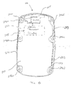
- FIG. 10 is a schematic diagram of a wireless communications device in accordance with another exemplary embodiment.
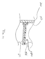
- FIG. 11 is a cross-sectional diagram of a portion of an electrically conductive continuous ring, multi-layer PCB, and a dielectric body in accordance with an exemplary embodiment.
- FIG. 12 is a perspective schematic view of a portion of the portable housing in FIG. 9 including electrically conductive shorting members.
- FIG. 13 is a schematic diagram of a PCB of a prototype mobile wireless communication device in accordance with an exemplary embodiment.
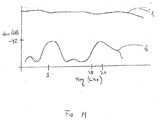
- FIG. 14 is a graph of the measured gain of a prototype mobile wireless communication device in accordance with an exemplary embodiment.
- a mobile wireless communications device may include a portable housing that may include an electrically conductive continuous ring that may define a perimeter of the portable housing.
- the electrically conductive continuous ring may be configured to function as an antenna, for example.
- a printed circuit board (PCB) may be carried by the portable housing and may include an electrically conductive layer defining a ground plane.
- Wireless transceiver circuitry may be carried by the PCB and coupled to the antenna.
- At least one electrically conductive shorting member may be coupled between the electrically conductive continuous ring and the ground plane, for example.
- the at least one electrically conductive shorting member may include a plurality of electrically conductive shorting members.
- the plurality of electrically conductive shorting members may be spaced apart, for example.
- the mobile wireless communications device may further include least one electrically floating member coupled between the electrically conductive continuous ring and the PCB, for example.
- the electrically conductive continuous ring may include metal, for example.
- the at least one electrically conductive shorting member may include at least one mechanical fastener.
- the at least one electrically conductive shorting member may include at least one conductive trace, for example.
- the PCB and the electrically conductive continuous ring may be positioned to define an air gap therebetween.
- the mobile wireless communications device may further include a dielectric material body between the PCB and the electrically conductive continuous ring, for example.
- the wireless transceiver circuitry may be configured to operate in the 800 MHz to 3.25 GHz frequency band, for example.
- a method aspect may be directed to a method of making a mobile wireless communications device.
- the method may include forming a portable housing having an electrically conductive continuous ring defining a perimeter thereof, for example.
- the electrically conductive continuous ring may be configured to function as an antenna.
- the method may further include positioning a printed circuit board (PCB) within the portable housing and comprising an electrically conductive layer defining a ground plane, and coupling wireless transceiver circuitry carried by the PCB to the antenna, for example.
- the method may further include coupling at least one electrically conductive shorting member between the electrically conductive continuous ring and the ground plane.
- PCB printed circuit board
- a mobile wireless communications device 30 illustratively includes a portable housing 31, a printed circuit board (PCB) 32 carried by the portable housing, and wireless transceiver circuitry 33 carried by the portable housing.
- the PCB 32 may be used in conjunction with a metal chassis or other substrate.
- the PCB 32 may also include a conductive layer defining a ground plane (not shown).
- the exemplary device 30 further illustratively includes a display 60 and a plurality of control keys including an "off hook” (i.e., initiate phone call) key 61, an "on hook” (i.e., discontinue phone call) key 62, a menu key 63, and a return or escape key 64. Operation of the various device components and input keys, etc., will be described further below with reference to FIG. 9 .
- a controller 66 or processor may also be carried by the PCB 32.
- the controller 66 may cooperate with the other components, for example, the antenna 35, the satellite positioning signal receiver 34, and the wireless transceiver circuitry 33 to coordinate and control operations of the mobile wireless communications device 30.
- Operations may include mobile voice and data operations, including email and Internet data.
- the portable housing 31 includes an electrically conductive portion.
- the portable housing 31 may be metallic or include a metallic portion.
- the electrically conductive portion functions as an antenna, and controlling the direction of current flowing the antenna becomes increasingly difficult.
- the portable conductive housing 31 including the electrically conductive portion configured to operate as an antenna may transmit or receive at different operating frequencies, for example, cellular telephone, satellite, or other wireless communications frequencies.
- the mobile wireless communications device 30 may include an additional or second antenna 35 coupled to the wireless transceiver circuitry 33.
- the second antenna 35 may also be configured to transmit or receive at different operating frequencies, for example, cellular telephone, satellite, or other wireless communications frequencies, and may operate independently or in conjunction with the electrically conductive portion of the portable conductive housing 31 that is configured as an antenna.
- One particularly advantageous approach to controlling the current flow includes forming a non-current carrying portion, using the portable housing 31 (configured as an antenna) and circuit elements 36 configured in an array.
- the circuit elements 36 may include orthogonal circuit components, for example, one or more of a capacitor and inductor.
- the circuit elements 36 may also include conductive traces, for example, on the PCB 32.
- the circuit elements 36 may be other components or elements, as will be appreciated by those skilled in the art.
- a shunt component 38 is coupled to the portable housing 31.
- the intersection of four circuit elements 36 and the shunt component 38 extending from the intersection 37 form a unit cell 40.
- the non-current carrying portion is formed by the cooperation of the array of circuit elements 36 and a shunt component 38.
- unit cells 40 may be used to define a current path for the current.
- a unit cell 40 configured as a passband unit cell illustratively includes four inductors as the circuit elements 36 and a capacitor as the shunt component 38.
- FIG. 3a unit cell 40 configured as a passband unit cell illustratively includes four inductors as the circuit elements 36 and a capacitor as the shunt component 38.
- a unit cell 40' configured as a stopband unit cell illustratively includes four capacitors as the circuit elements 36' and a capacitor as the shunt component 38'.
- circuit elements 36 and shunt conductors 38 may be used, for example, as illustrated in FIGS. 3c and 3d , and the shunt conductor may include more than one shunt conductor.
- unit cell 40 when the spacing between adjacent circuit elements 36 is relatively much less than the desired operating wavelength, the unit cell 40 may exhibit electromagnetic characteristics that may be adjusted to desired specifications. Accordingly, unit cells 40 including the circuit elements 36 and the shunt conductor 38 may be characterized by macro quantities, such as permittivity or permeability, for example.
- macro quantities such as permittivity or permeability, for example.
- equation (9) is always real. In other words, propagation is allowed for all frequencies from zero to the self-resonance frequency of the circuit components 36.
- the portable housing 31, the circuit elements 36 (i.e. series inductors), and the shunt component 38 cooperate to form a passband condition ( FIG. 3a ).
- any number or combination of circuit components may be used so long as k is imaginary.
- a combination of passband unit cells 40 and stopband unit cells 40' may be configured to direct currents from the antenna 35.
- a combination of passband and stopband unit cells 40, 40', 40", 40'” may be arranged to direct the flow of current through the portable housing 31.
- the current will flow away from the point of excitation, but may be confined by the stopband unit cells 40' and flow in areas of the passband cells 40.
- antenna design in a device having a full metal portable housing may focus on the arrangement of the passband unit cells 40 into a shape and size that produces the desired radiation pattern.
- a mobile wireless communications device 30 including an array, or a layer, of circuit elements 36 may not be desirable, as additional components may increase the weight of the mobile wireless communications device.
- the circuit elements 36 may be the circuit components carried on the PCB 32, for example, the wireless transceiver circuitry 33.
- the array of spaced apart circuit components 36 and the shunt component 38 advantageously cooperate to enable radiation with a mobile wireless communications device having an electrically conductive housing.
- growing industrial design trends include metallic materials, for example, to convey a sense of increased quality.
- many mobile wireless communications devices include relatively increased quantities of metallic materials.
- Some of these mobile wireless communications devices also include a radiating element, or an antenna, that is integrated into a structure including the metallic materials, for example, a metal ring.
- the metal ring or electrically conductive material portion of the portable housing also functions as an antenna.
- the radiating element may be positioned away from the metallic materials (e.g. metallic housing).
- a metallic material may include a material that behaves like a conductor in the radio frequency (RF) band.
- a metallic material may include a liquid crystal display (LCD), as the glass is embedded with micro-wires that would appear as a conducting plate to an electromagnetic wave.
- LCD liquid crystal display
- the mobile wireless communications device 30"" includes a multi-layer PCB 32"'' that includes a first conductive layer 51"" (i.e. the ground plane), a dielectric layer 54'''', and a second conductive layer 52'''' separated from the first conductive layer by a second dielectric layer 53''''.
- the second dielectric layer 53'''' may be a layer of air, or may be another dielectric material, as will be appreciated by those skilled in the art.
- the shunt conductor 38'''' couples the first and second conductive layers 51'''', 52''''.
- the second conductive layer 51'''' may include the circuit elements 36'''' or conductive traces (not shown) on the PCB 32''''.
- one or more of the circuit elements 36 may be carried by a flexible substrate (not shown).
- the flexible circuit substrate which may be either attached to the PCB 32 or separate from the PCB, may carry the circuit elements 36 or include a metallization layer that acts as the circuit elements.
- the flexible circuit substrate may be Kapton TM , for example.
- a prototype mobile wireless communications device similar to the mobile wireless communications device 30 described above was made and covered with copper to emulate a completely metallic portable housing.
- the antenna was configured for operation at the GPS frequency of 1.575 GHz.
- the PCB had a plurality of shunt components configured in a semi-circular configuration and coupling the metallic portable housing to the ground plane of the PCB.
- the measured radiation pattern of the prototype GPS antenna of the prototype is illustrated.
- the measured gain is roughly -7.5 dBi, which is relatively comparable with the antenna gain of other GPS antennas.
- the portable housing 131 includes a metal ring 145 positioned along a perimeter of the portable housing and configured to function as a part of an antenna.
- the metal ring 145 causes increased degradation in radiated performance from the hand phantom condition, as will be appreciated by those skilled in the art. A relatively large magnitude of current was found to flow in the metal ring 145 where the user's hand would come into contact therewith. As such, a majority of the current or radiation was directed into the user's hand.
- a non-current carrying portion is adjacent the side of the mobile wireless communications device 130.
- the non-current carrying portion is created by cooperation between the metal ring 145, the PCB 132, and the antenna feed location.
- the metal ring 145 makes contact with the PCB 132 via the screw mounts 146 around the metal ring.
- the non-current carrying portion is achieved by isolating the screw mounts 146 near the antenna feedpoint.
- the non-current carrying portion length is defined by distance between the grounding points (i.e. the other three screw mounts that are not coupled to the shunt components 138 ) and the loading elements, or the shunt components, along the non-current carrying portion.
- the shunt components 138 that couple the metal ring 145 to the PCB 132 are adjusted such that the propagation constant along the metal ring becomes imaginary. Additionally, an air gap 149 is between the PCB 132 and the metal ring 145 along the non-current carrying portion.
- Table 1 the results of two measurements performed, one with a non-current carrying portion in accordance with the present embodiments, (Table 1) and another without a non-current carrying portion (Table 2), are shown. Indeed, as will be appreciated by those skilled in the art, the measurements show that the hand-phantom performance of the non-current carrying portion implementation is an improvement across the bands with as much as 5 dB.
- Table 1 Tx Rx Band L M H L M H 1800 -10.44 -10.23 -10.88 -10.98 -10.97 -11.61 1900 -11.20 -11.69 -11.48 -12.10 -12.33 -12.62 2100 -11.83 -12.24 -11.96 -11.96 -13.38 -15.61 Table 2.
- the non-current carrying portion may be programmable.
- the non-current carrying portion may not be limited to a fixed range of frequencies.
- the shunt components 38 allow fine-tuning of the wave vector. Accordingly, the shunt components 38 may be replaced by a programmable network device, such as may be available from Murata Manufacturing, Co. Ltd. of Japan, or Epcos AG of Germany.
- the iPhoneTM 4G for example, which also uses its inherent structural metal band as a radiating element, uses a broken structure as a radiating element or antenna.
- the metal ring 145 of the present embodiments encompasses the entire perimeter of the mobile wireless communications device 130, and there are no cuts or parting lines in the metal ring. Accordingly, the integrity of the portable housing 131 remains intact.
- the iPhoneTM 4G uses a broken structure band as its radiating element, and is tuned to several frequencies.
- a portion of the structure is responsible for radiation. This is achieved by reducing the two-dimensional (2D) non-current carrying portion approach into a one-dimensional (1D) form.
- a PCB may act like a ground plane, where the propagating power is trapped by the parallel-plate TEM mode that degrades the overall radiation efficiency.
- an external antenna may be used; however, this would be contrary to the current industrial design trend, where it is desirable that all antennas be internal to the device housing.
- a method aspect is directed to a method of making a mobile wireless communications device 30 that includes a portable housing 31 including at least one electrically conductive housing portion configured to function as an antenna, a printed circuit board (PCB) 32 carried by the portable housing, and wireless transceiver circuitry 33 carried by the PCB and including at least one circuit element 36 carried by the PCB.
- the method includes coupling at least one current shunt component 38 between the at least one electrically conductive portion 31 and the at least one circuit element 36.
- the device 1000 illustratively includes a housing 1200, a keypad 1400 and an output device 1600.
- the output device shown is a display 1600, which may comprise a full graphic LCD.
- display 1600 may comprise a touch-sensitive input and output device.
- a processing device 1800 is contained within the housing 1200 and is coupled between the keypad 1400 and the display 1600. The processing device 1800 controls the operation of the display 1600, as well as the overall operation of the mobile device 1000, in response to actuation of keys on the keypad 1400 by the user.
- keypad 1400 may comprise a physical keypad or a virtual keypad (e.g., using a touch-sensitive interface) or both.
- the housing 1200 may be elongated vertically, or may take on other sizes and shapes (including clamshell housing structures, for example).
- the keypad 1400 may include a mode selection key, or other hardware or software for switching between text entry and telephony entry.
- FIG. 9 In addition to the processing device 1800, other parts of the mobile device 1000 are shown schematically in FIG. 9 . These include a communications subsystem 1001; a short-range communications subsystem 1020; the keypad 1400 and the display 1600, along with other input/output devices 1060, 1080, 1100 and 1120; as well as memory devices 1160, 1180 and various other device subsystems 1201.
- the mobile device 1000 may comprise a two-way RF communications device having voice and data communications capabilities.
- the mobile device 1000 may have the capability to communicate with other computer systems via the Internet.
- Operating system software executed by the processing device 1800 may be stored in a persistent store, such as the flash memory 1160, but may be stored in other types of memory devices, such as a read only memory (ROM) or similar storage element.
- system software, specific device applications, or parts thereof may be temporarily loaded into a volatile store, such as the random access memory (RAM) 1180. Communications signals received by the mobile device may also be stored in the RAM 1180.
- the processing device 1800 in addition to its operating system functions, enables execution of software applications or modules 1300A-1300N on the device 1000, such as software modules for performing various steps or operations.
- a predetermined set of applications that control basic device operations, such as data and voice communications 1300A and 1300B, may be installed on the device 1000 during manufacture.
- a personal information manager (PIM) application may be installed during manufacture.
- the PIM may be capable of organizing and managing data items, such as e-mail, calendar events, voice mails, appointments, and task items.
- the PIM application may also be capable of sending and receiving data items via a wireless network 1401.
- the PIM data items may be seamlessly integrated, synchronized and updated via the wireless network 1401 with the device user's corresponding data items stored or associated with a host computer system.
- the communications subsystem 1001 includes a receiver 1500, a transmitter 1520, and one or more antennas 1540 and 1560.
- the communications subsystem 1001 also includes a processing module, such as a digital signal processor (DSP) 1580, and local oscillators (LOs) 1601.
- DSP digital signal processor
- LOs local oscillators
- a mobile device 1000 may include a communications subsystem 1001 designed to operate with the Mobitex TM , Data TAC TM or General Packet Radio Service (GPRS) mobile data communications networks, and also designed to operate with any of a variety of voice communications networks, such as AMPS, TDMA, CDMA, WCDMA, PCS, GSM, EDGE, etc. Other types of data and voice networks, both separate and integrated, may also be utilized with the mobile device 1000.
- the mobile device 1000 may also be compliant with other communications standards such as GSM, 3G, UMTS, 4G, etc.
- Network access requirements vary depending upon the type of communication system. For example, in the Mobitex and DataTAC networks, mobile devices are registered on the network using a unique personal identification number or PIN associated with each device. In GPRS networks, however, network access is associated with a subscriber or user of a device. A GPRS device therefore utilizes a subscriber identity module, commonly referred to as a SIM card, in order to operate on a GPRS network.
- SIM card subscriber identity module
- the mobile device 1000 may send and receive communications signals over the communication network 1401.
- Signals received from the communications network 1401 by the antenna 1540 are routed to the receiver 1500, which provides for signal amplification, frequency down conversion, filtering, channel selection, etc., and may also provide analog to digital conversion. Analog-to-digital conversion of the received signal allows the DSP 1580 to perform more complex communications functions, such as demodulation and decoding.
- signals to be transmitted to the network 1401 are processed (e.g. modulated and encoded) by the DSP 1580 and are then provided to the transmitter 1520 for digital to analog conversion, frequency up conversion, filtering, amplification and transmission to the communication network 1401 (or networks) via the antenna 1560.
- the DSP 1580 provides for control of the receiver 1500 and the transmitter 1520. For example, gains applied to communications signals in the receiver 1500 and transmitter 1520 may be adaptively controlled through automatic gain control algorithms implemented in the DSP 1580.
- a received signal such as a text message or web page download
- the communications subsystem 1001 is input to the processing device 1800.
- the received signal is then further processed by the processing device 1800 for an output to the display 1600, or alternatively to some other auxiliary I/O device 1060.
- a device user may also compose data items, such as e-mail messages, using the keypad 1400 and/or some other auxiliary I/O device 1060, such as a touchpad, a rocker switch, a thumb-wheel, or some other type of input device.
- the composed data items may then be transmitted over the communications network 1401 via the communications subsystem 1001.
- a voice communications mode In a voice communications mode, overall operation of the device is substantially similar to the data communications mode, except that received signals are output to a speaker 1100, and signals for transmission are generated by a microphone 1120.
- Alternative voice or audio I/O subsystems such as a voice message recording subsystem, may also be implemented on the device 1000.
- the display 1600 may also be utilized in voice communications mode, for example to display the identity of a calling party, the duration of a voice call, or other voice call related information.
- the short-range communications subsystem enables communication between the mobile device 1000 and other proximate systems or devices, which need not necessarily be similar devices.
- the short-range communications subsystem 1020 may include an infrared device and associated circuits and components, near-field communication (NFC), or a Bluetooth TM communications module to provide for communication with similarly-enabled systems and devices.
- NFC near-field communication
- Bluetooth TM communications module to provide for communication with similarly-enabled systems and devices.
- a mobile wireless communications device 230 illustratively includes a portable housing 231 that includes an electrically conductive continuous ring 245 that defines a perimeter of the portable housing.
- the electrically conductive continuous ring 245 is configured to function as an antenna.
- the electrically conductive continuous ring 245 may include metal, for example.
- the electrically conductive continuous ring 245 may be another conductive material, as will be appreciated by those skilled in the art.
- a printed circuit board (PCB) 232 is also illustratively carried by the portable housing 231.
- the PCB 232 includes a dielectric layer 258 and an electrically conductive layer 251 defining a ground plane carried by the dielectric layer ( FIG. 11 ).
- Wireless transceiver circuitry 233 is carried by the PCB 232 and coupled to the antenna or electrically conductive continuous ring 245.
- the wireless transceiver circuitry 233 may be configured to operate in the 800 MHz to 3.25 GHz frequency band, for example.
- the wireless transceiver circuitry 233 may be configured to operate at other frequency bands.
- An additional or second antenna 235 is coupled to the wireless transceiver circuitry 233.
- the second antenna 235 may be used together or separately from the antenna provided by the electrically conductive continuous ring 245 to perform wireless communications.
- Spaced apart electrically conductive shorting members are coupled between the electrically conductive continuous ring 245 and the ground plane 251.
- mechanical fasteners 246b-246e i.e. screws cooperating with respective screw terminals or mounts, are electrically conductive and shorted to the ground plane 251.
- the electrically conductive shorting members also include conductive traces 247a, 247b shorting the electrically conductive continuous ring 245 to the ground plane 251 ( FIG. 12 ).
- a metal tap 252 also shorts the electrically conductive continuous ring 245 to the ground plane 251 ( FIG. 12 ).
- additional types of electrically conductive shorting members may be used.
- any combination and number of the different types of electrically conductive shorting members may be used, as will be appreciated by those skilled in the art.
- Electrically floating members are also coupled between the electrically conductive continuous ring 245 and the PCB 232.
- one or more of the mechanical fasteners 246, for example, 246a, 246f may be electrically floating.
- the electrically floating members 246a, 246f advantageously cooperate with the electrically conductive shorting members 246b-246e, 247a, 247b, 252 to direct current through the electrically conductive continuous ring 245 or antenna, as will be appreciated by those skilled in the art. Indeed, by directing currents through the electrically conductive continuous ring 245, the radiation pattern thereof may be adjusted for improved communications.
- the configuration of the electrically conductive shorting members and electrically floating members may be changed or configured for a desired current direction.
- the mechanical fasteners 246 and/or other members may be configured as either electrically shorting or electrically floating, and additional or other shorting members may be included at a desired location or locations.
- the PCB 232 and the electrically conductive continuous ring 245 are illustratively positioned to define an air gap 249 therebetween.
- the air gap 249 may be particularly advantageous for cooperating with the electrically conductive shorting members and electrically floating members to create a non-current carrying portion, for example.
- the mobile wireless communications device 230 may also include a dielectric material body 253 between the PCB 232 and the electrically conductive continuous ring 245, for example.
- a prototype mobile wireless communications device was formed.
- the PCB layout ( FIG. 13 ) of the prototype included a battery connector (not shown).
- the positive terminal of the battery connector is coupled to the ground through shunt capacitors (not shown).
- the shunt capacitors mimic the actual system behavior where the positive terminal is capacitive at RF frequencies.
- the PCB layout of the prototype also included a reconfigurable antenna feed 255' and a reconfigurable speaker feed 254' ( FIG. 13 ) with chokes (not shown). High band performance may be increased if the speaker feed 254' is used to shunt a portion of antenna current to the PCB 232'.
- the measured response S 21 without the speaker module and the antenna is also illustrated. Indeed, when the speaker springs were removed, the gain response at about 2.0 GHz was increased by about 1 to 1.8 dB.
- the electrically conductive continuous ring has multiple types of degradation.
- the two mechanical fasteners or screws and respective screw terminals 246a, 246f generally limit that antenna bandwidth when they are shorted to ground, for example.
- the two mechanical fasteners 246a, 246f are floating, they introduce a destructive interference at the low band, for example, around 800 MHz.
- the destructive interference may be mitigated by introducing a short between the electrically conductive continuous ring 245 and ground plane 251 at location 255.
- the electrically conductive continuous ring 245 may be shorted at location 255 by any of the above-noted structures, e.g. mechanical fastener, conductive trace, conductive structural support, etc. While a short at location 255 may not completely eliminate the transmission line effect between the PCB 232 and the electrically conductive continuous ring 245, it generally shifts the destructive interference outside of the operating frequency band.
- Mechanical fasteners 246b, 246e provide additional shorting to achieve the desired operating characteristics. Of course, the number or location of the shorts may be altered to achieve desired operational characteristics.
- the speaker causes a relatively small shift in the frequency response of the antenna 245.
- the second resonance which is about 1.7 GHz, generally decreases in frequency when the speaker is present. This phenomenon could also be duplicated by placing a ferrite material to create a short between the two structural speaker support brackets.
- the high band response shifts lower and the gain is also reduced.
- the speaker feed grounding 259 FIG. 12
- high band response increased by about 0.3 dB.
- reducing the choke inductance from 68 nH to 27 nH shifts the low band interference from around 780 MHz to 1.1 GHz. This reduces the second low band interference that was originally masked by the transmission line effect at the screws and terminals 246a, 246b, and location 255 ( FIG. 10 ).
- a method aspect may be directed to a method of making a mobile wireless communications device 230.
- the method includes forming a portable housing 231 having an electrically conductive continuous ring 245 defining a perimeter thereof.
- the electrically conductive continuous ring 245 is configured to function as an antenna.
- the method further includes positioning a printed circuit board (PCB) 232 within the portable housing 231 and comprising an electrically conductive layer defining a ground plane 251.
- the method further includes coupling wireless transceiver circuitry 233 carried by the PCB 232 to the antenna 245.
- the method also includes coupling at least one electrically conductive shorting member 246, 247, 252 between the electrically conductive continuous ring 245 and the ground plane 251.
Landscapes
- Engineering & Computer Science (AREA)
- Computer Networks & Wireless Communication (AREA)
- Support Of Aerials (AREA)
- Telephone Set Structure (AREA)
Abstract
Description
- The present application is based upon previously filed copending provisional application Serial No.
61/367,113, filed July 23, 2010 13/005,311, filed January 12, 2011 13/099,025, filed May 2, 2011 - The present disclosure generally relates to the field of wireless communications systems, and, more particularly, to mobile wireless communications devices and related methods.
- Mobile wireless communications systems continue to grow in popularity and have become an integral part of both personal and business communications. For example, cellular telephones allow users to place and receive voice calls almost anywhere they travel. Moreover, as cellular telephone technology has increased, so too has the functionality of cellular devices and the different types of devices available to users. For example, many cellular devices now incorporate personal digital assistant (PDA) features such as calendars, address books, task lists, etc. Moreover, such multi-function devices may also allow users to wirelessly send and receive electronic mail (email) messages and access the Internet via a cellular network and/or a wireless local area network (WLAN), for example.
- Even so, as the functionality of cellular communications devices continues to increase, so too does the demand for smaller devices which are easier and more convenient for users to carry. One challenge this poses for cellular device manufacturers is designing housings that cooperate with antennas to provide desired operating characteristics within the relatively limited amount of space available.
-
FIG. 1 is a front view of a mobile wireless communications device including a shunt conductor in accordance with one exemplary aspect. -
FIG. 2 is a schematic diagram of the printed circuit board (PCB) and the housing of the device ofFIG. 1 . -
FIGS. 3a-3d are schematic diagrams of circuit elements and a shunt conductor in accordance with exemplary embodiments. -
FIG. 4 is a schematic diagram of an arrangement of passband and stopband cells in accordance with an exemplary embodiment. -
FIG. 5 is a cross-sectional diagram of a multi-layer PCB in accordance with an exemplary embodiment. -
FIG. 6 is a graph of measured radiation of an antenna of a mobile wireless communication device in accordance with an exemplary embodiment. -
FIG. 7 is a schematic diagram of a portion of a PCB and housing of a mobile wireless communications device in accordance with an exemplary embodiment. -
FIG. 8 is an enlarged view of a portion of the PCB and housing ofFIG. 7 . -
FIG. 9 is a schematic block diagram illustrating additional components that may be included in the mobile wireless communications device ofFIG. 1 . -
FIG. 10 is a schematic diagram of a wireless communications device in accordance with another exemplary embodiment. -
FIG. 11 is a cross-sectional diagram of a portion of an electrically conductive continuous ring, multi-layer PCB, and a dielectric body in accordance with an exemplary embodiment. -
FIG. 12 is a perspective schematic view of a portion of the portable housing inFIG. 9 including electrically conductive shorting members. -
FIG. 13 is a schematic diagram of a PCB of a prototype mobile wireless communication device in accordance with an exemplary embodiment. -
FIG. 14 is a graph of the measured gain of a prototype mobile wireless communication device in accordance with an exemplary embodiment. - The present description is made with reference to the accompanying drawings, in which various embodiments are shown. However, many different embodiments may be used, and thus the description should not be construed as limited to the embodiments set forth herein. Rather, these embodiments are provided so that this disclosure will be thorough and complete. Like numbers refer to like elements throughout and prime notation is used to indicate similar elements in alternative embodiments.
- In accordance with one exemplary aspect, a mobile wireless communications device may include a portable housing that may include an electrically conductive continuous ring that may define a perimeter of the portable housing. The electrically conductive continuous ring may be configured to function as an antenna, for example. A printed circuit board (PCB) may be carried by the portable housing and may include an electrically conductive layer defining a ground plane. Wireless transceiver circuitry may be carried by the PCB and coupled to the antenna. At least one electrically conductive shorting member may be coupled between the electrically conductive continuous ring and the ground plane, for example.
- The at least one electrically conductive shorting member may include a plurality of electrically conductive shorting members. The plurality of electrically conductive shorting members may be spaced apart, for example.
- The mobile wireless communications device may further include least one electrically floating member coupled between the electrically conductive continuous ring and the PCB, for example. The electrically conductive continuous ring may include metal, for example.
- The at least one electrically conductive shorting member may include at least one mechanical fastener. The at least one electrically conductive shorting member may include at least one conductive trace, for example.
- The PCB and the electrically conductive continuous ring may be positioned to define an air gap therebetween. The mobile wireless communications device may further include a dielectric material body between the PCB and the electrically conductive continuous ring, for example. The wireless transceiver circuitry may be configured to operate in the 800 MHz to 3.25 GHz frequency band, for example.
- A method aspect may be directed to a method of making a mobile wireless communications device. The method may include forming a portable housing having an electrically conductive continuous ring defining a perimeter thereof, for example. The electrically conductive continuous ring may be configured to function as an antenna. The method may further include positioning a printed circuit board (PCB) within the portable housing and comprising an electrically conductive layer defining a ground plane, and coupling wireless transceiver circuitry carried by the PCB to the antenna, for example. The method may further include coupling at least one electrically conductive shorting member between the electrically conductive continuous ring and the ground plane.
- Referring initially to
FIGS. 1-3 , a mobilewireless communications device 30 illustratively includes aportable housing 31, a printed circuit board (PCB) 32 carried by the portable housing, andwireless transceiver circuitry 33 carried by the portable housing. In other embodiments, the PCB 32 may be used in conjunction with a metal chassis or other substrate. ThePCB 32 may also include a conductive layer defining a ground plane (not shown). - A satellite
positioning signal receiver 34 is also carried by theportable housing 31. The satellitepositioning signal receiver 34 may be a Global Positioning System (GPS) satellite receiver, for example. - The
exemplary device 30 further illustratively includes adisplay 60 and a plurality of control keys including an "off hook" (i.e., initiate phone call)key 61, an "on hook" (i.e., discontinue phone call)key 62, amenu key 63, and a return orescape key 64. Operation of the various device components and input keys, etc., will be described further below with reference toFIG. 9 . - A
controller 66 or processor may also be carried by the PCB 32. Thecontroller 66 may cooperate with the other components, for example, theantenna 35, the satellitepositioning signal receiver 34, and thewireless transceiver circuitry 33 to coordinate and control operations of the mobilewireless communications device 30. Operations may include mobile voice and data operations, including email and Internet data. - The
portable housing 31 includes an electrically conductive portion. For example, theportable housing 31 may be metallic or include a metallic portion. As will be appreciated by those skilled in the art, when aportable housing 31 includes an electrically conductive portion, the electrically conductive portion functions as an antenna, and controlling the direction of current flowing the antenna becomes increasingly difficult. - The portable
conductive housing 31 including the electrically conductive portion configured to operate as an antenna may transmit or receive at different operating frequencies, for example, cellular telephone, satellite, or other wireless communications frequencies. The mobilewireless communications device 30 may include an additional orsecond antenna 35 coupled to thewireless transceiver circuitry 33. Thesecond antenna 35 may also be configured to transmit or receive at different operating frequencies, for example, cellular telephone, satellite, or other wireless communications frequencies, and may operate independently or in conjunction with the electrically conductive portion of the portableconductive housing 31 that is configured as an antenna. - One particularly advantageous approach to controlling the current flow includes forming a non-current carrying portion, using the portable housing 31 (configured as an antenna) and
circuit elements 36 configured in an array. Thecircuit elements 36 may include orthogonal circuit components, for example, one or more of a capacitor and inductor. Thecircuit elements 36 may also include conductive traces, for example, on thePCB 32. Thecircuit elements 36 may be other components or elements, as will be appreciated by those skilled in the art. - At each common node or
intersection 37 of thecircuit elements 36, ashunt component 38 is coupled to theportable housing 31. The intersection of fourcircuit elements 36 and theshunt component 38 extending from theintersection 37 form aunit cell 40. As will be appreciated by those skilled in the art, the non-current carrying portion is formed by the cooperation of the array ofcircuit elements 36 and ashunt component 38. In other words,unit cells 40 may be used to define a current path for the current. For example, as illustrated inFIG. 3a , aunit cell 40 configured as a passband unit cell illustratively includes four inductors as thecircuit elements 36 and a capacitor as theshunt component 38. Alternatively, as illustrated inFIG. 3b , a unit cell 40' configured as a stopband unit cell illustratively includes four capacitors as the circuit elements 36' and a capacitor as the shunt component 38'. Of course, other types ofcircuit elements 36 andshunt conductors 38 may be used, for example, as illustrated inFIGS. 3c and 3d , and the shunt conductor may include more than one shunt conductor. - Additionally, when the spacing between
adjacent circuit elements 36 is relatively much less than the desired operating wavelength, theunit cell 40 may exhibit electromagnetic characteristics that may be adjusted to desired specifications. Accordingly,unit cells 40 including thecircuit elements 36 and theshunt conductor 38 may be characterized by macro quantities, such as permittivity or permeability, for example. Using the quasi-transverse electromagnetic mode (quasi-TEM) approximation within aunit cell 40, as disclosed in J. K. H. Wong, K. G. Balmain, and G. V. Eleftheriades, "Fields in planar anisotropic transmission-line metamaterials," vol. 54, no. 10, pp. 2742- 2749, Oct. 2006, the non-zero field components are:


- This configuration allows the propagation of waves where the electric fields are polarized vertically between the
unit cells 40 and theportable housing 31. If the separation between theunit cells 40 and theportable housing 31 is made sufficiently small, the fields within the volume bounded by the unit cells and the portable housing is approximately uniform in the z direction. In other words, ∂/∂z = 0 and equations (1a-1c) apply. Considering the H-mode fields, equations (1a) and (1b) are integrated to obtain:

- Next, equation (2) is integrated along the x and the y directions to obtain:


- The currents flowing through the
circuit elements 36, i.e. the capacitors and the inductors are determined by the voltage difference across aunit cell 40 and can be expressed as:

- In equations (4a-4b), Xx and Xy are respectively, the reactance along the x and the y directions at the wave frequency. Substituting equation (4) into equation (3) and assuming d = Δx = Δy = Δz:


- For the
unit cell 40 illustrated inFIG. 3a , the reactance along the x and the y directions are equal and can be represented as
where L is the series loaded inductance and L 0 is the inductance per unit length of the interconnecting transmission line. Therefore, equation (6) can be substituted into equation (5) to arrive at the expressions that relate the permeabilities and the lumped component values which is:
- Applying the same procedure to the Ampere's law, (1c), one would arrive at an expression relating the
shunt component 38 value to the permittivity which is:
where Cshunt is the shunt capacitance and C 0 is the capacitance per unit length of the interconnecting transmission-line. - Having calculated the effective permittivity and the permeability, the propagation constant within the
portable housing 31 and the array ofcircuit components 36 may be derived such that:
- Assuming that the operating frequency is relatively well below the self-resonance frequency of the circuit components 36 (i.e., the inductors and the capacitors), equation (9) is always real. In other words, propagation is allowed for all frequencies from zero to the self-resonance frequency of the
circuit components 36. Thus, theportable housing 31, the circuit elements 36 (i.e. series inductors), and theshunt component 38 cooperate to form a passband condition (FIG. 3a ). - To create a stopband condition, k must be made imaginary. Accordingly, if the circuit component 36' is a capacitor as shown in
FIG. 3b . we get
Substituting equation (10) into equation (5):
Thus, propagation in such as structure is given by
From (12), one can observe that the wave vector becomes imaginary when the following condition holds
In other words, a stopband condition can be achieved within a desired frequency range by varying C. As will be appreciated by those skilled in the art, to create a stopband, any number or combination of circuit components may be used so long as k is imaginary. Additionally, a combination ofpassband unit cells 40 and stopband unit cells 40' may be configured to direct currents from theantenna 35. - Referring now to
FIG. 4 , a combination of passband andstopband unit cells portable housing 31. When theportable housing 31 is excited with current from theantenna 35, the current will flow away from the point of excitation, but may be confined by the stopband unit cells 40' and flow in areas of thepassband cells 40. Thus, as will be appreciated by those skilled in the art, antenna design in a device having a full metal portable housing may focus on the arrangement of thepassband unit cells 40 into a shape and size that produces the desired radiation pattern. - However, given the relatively small size of a mobile
wireless communications device 30, it may be desirable to further reduce the amount of discrete physical components used for directing the current or creating the non-current carrying portion. In other words, a mobilewireless communications device 30 including an array, or a layer, ofcircuit elements 36 may not be desirable, as additional components may increase the weight of the mobile wireless communications device. In such a case, thecircuit elements 36 may be the circuit components carried on thePCB 32, for example, thewireless transceiver circuitry 33. - As will be appreciated by those skilled in the art, the array of spaced apart
circuit components 36 and theshunt component 38 advantageously cooperate to enable radiation with a mobile wireless communications device having an electrically conductive housing. Indeed, growing industrial design trends include metallic materials, for example, to convey a sense of increased quality. - Accordingly, many mobile wireless communications devices include relatively increased quantities of metallic materials. Some of these mobile wireless communications devices also include a radiating element, or an antenna, that is integrated into a structure including the metallic materials, for example, a metal ring. In other words, the metal ring or electrically conductive material portion of the portable housing also functions as an antenna. Alternatively, in some mobile wireless communications devices, the radiating element may be positioned away from the metallic materials (e.g. metallic housing).
- The
circuit components 36 and theshunt component 38 advantageously enable wireless communications via an internal antenna that may be completely covered with a metallic material, for example. Indeed, as will be appreciated by those skilled in the art, a metallic material may include a material that behaves like a conductor in the radio frequency (RF) band. For example, a metallic material may include a liquid crystal display (LCD), as the glass is embedded with micro-wires that would appear as a conducting plate to an electromagnetic wave. - Referring now to
FIG. 5 , in another exemplary embodiment, the mobilewireless communications device 30"" includes amulti-layer PCB 32"'' that includes a firstconductive layer 51"" (i.e. the ground plane), a dielectric layer 54'''', and a second conductive layer 52'''' separated from the first conductive layer by a second dielectric layer 53''''. The second dielectric layer 53'''' may be a layer of air, or may be another dielectric material, as will be appreciated by those skilled in the art. The shunt conductor 38'''' couples the first and second conductive layers 51'''', 52''''. The second conductive layer 51'''' may include the circuit elements 36'''' or conductive traces (not shown) on the PCB 32''''. - Still further, in some exemplary embodiments, one or more of the
circuit elements 36 may be carried by a flexible substrate (not shown). The flexible circuit substrate, which may be either attached to thePCB 32 or separate from the PCB, may carry thecircuit elements 36 or include a metallization layer that acts as the circuit elements. The flexible circuit substrate may be Kapton™, for example. - A prototype mobile wireless communications device similar to the mobile
wireless communications device 30 described above was made and covered with copper to emulate a completely metallic portable housing. The antenna was configured for operation at the GPS frequency of 1.575 GHz. The PCB had a plurality of shunt components configured in a semi-circular configuration and coupling the metallic portable housing to the ground plane of the PCB. - Referring additionally to the
graph 71 inFIG. 6 , the measured radiation pattern of the prototype GPS antenna of the prototype is illustrated. The measured gain is roughly -7.5 dBi, which is relatively comparable with the antenna gain of other GPS antennas. - Referring now to
FIGS. 7-8 , another embodiment of the mobilewireless communications device 130 according to an exemplary aspect is described. Illustratively, the portable housing 131 includes ametal ring 145 positioned along a perimeter of the portable housing and configured to function as a part of an antenna. Themetal ring 145 causes increased degradation in radiated performance from the hand phantom condition, as will be appreciated by those skilled in the art. A relatively large magnitude of current was found to flow in themetal ring 145 where the user's hand would come into contact therewith. As such, a majority of the current or radiation was directed into the user's hand. - To reduce the current flowing on the
metal ring 145 with a relatively small, if any, reduction in antenna radiation performance, a non-current carrying portion is adjacent the side of the mobilewireless communications device 130. The non-current carrying portion, is created by cooperation between themetal ring 145, thePCB 132, and the antenna feed location. - The
metal ring 145 makes contact with thePCB 132 via the screw mounts 146 around the metal ring. The non-current carrying portion is achieved by isolating the screw mounts 146 near the antenna feedpoint. The non-current carrying portion length is defined by distance between the grounding points (i.e. the other three screw mounts that are not coupled to the shunt components 138) and the loading elements, or the shunt components, along the non-current carrying portion. To create the non-current carrying portion, theshunt components 138 that couple themetal ring 145 to thePCB 132 are adjusted such that the propagation constant along the metal ring becomes imaginary. Additionally, anair gap 149 is between thePCB 132 and themetal ring 145 along the non-current carrying portion. - Referring now to Tables 1 and 2, the results of two measurements performed, one with a non-current carrying portion in accordance with the present embodiments, (Table 1) and another without a non-current carrying portion (Table 2), are shown. Indeed, as will be appreciated by those skilled in the art, the measurements show that the hand-phantom performance of the non-current carrying portion implementation is an improvement across the bands with as much as 5 dB.
Table 1. Tx Rx Band L M H L M H 1800 -10.44 -10.23 -10.88 -10.98 -10.97 -11.61 1900 -11.20 -11.69 -11.48 -12.10 -12.33 -12.62 2100 -11.83 -12.24 -11.96 -11.96 -13.38 -15.61 Table 2. Tx Rx Band L M H L M H 1800 -9.66 -9.12 -9.47 -9.65 -8.86 -9.06 1900 -8.90 -9.10 -8.23 -8.77 -8.23 -8.44 2100 -8.44 -8.57 -7.83 -8.50 -8.75 -8.63 - In some embodiments, not shown, the non-current carrying portion, may be programmable. In other words, the non-current carrying portion may not be limited to a fixed range of frequencies. As will be appreciated by those skilled in the art, the
shunt components 38 allow fine-tuning of the wave vector. Accordingly, theshunt components 38 may be replaced by a programmable network device, such as may be available from Murata Manufacturing, Co. Ltd. of Japan, or Epcos AG of Germany. - In contrast to the mobile wireless communications device described herein, the iPhone™ 4G, for example, which also uses its inherent structural metal band as a radiating element, uses a broken structure as a radiating element or antenna. Indeed, the
metal ring 145 of the present embodiments encompasses the entire perimeter of the mobilewireless communications device 130, and there are no cuts or parting lines in the metal ring. Accordingly, the integrity of the portable housing 131 remains intact. - Moreover, the iPhone™ 4G uses a broken structure band as its radiating element, and is tuned to several frequencies. In contrast, in the present embodiments, a portion of the structure is responsible for radiation.
This is achieved by reducing the two-dimensional (2D) non-current carrying portion approach into a one-dimensional (1D) form. - Existing approaches for wirelessly communicating using a mobile wireless communications device having a full metal housing or enclosure were developed for aircrafts, missiles, land/naval armored vehicles, or radar systems, for example, as disclosed by F. D. Bennett, P. D. Coleman, and A. S. Meier in, "The design of broadband aircraft-antenna systems," Proceedings of I.R.E., pp. 671-700, Oct. 1954, and by H. G. Booker in "Slot aerials and their relation to complementary wire aerials (Babinet's principle)," Journal of I.E.E., no. 93, p. 620, 1946. These approaches employed either slots (magnetic currents) or external antennas for controlling the radiation pattern. Magnetic currents can be created by slots or an aperture in a conductive plate. This method is relatively more difficult to implement in a mobile wireless communications device, as the slot length is restricted by the device size and the industrial design requirements.
- Furthermore, in a mobile wireless communications device environment, a PCB may act like a ground plane, where the propagating power is trapped by the parallel-plate TEM mode that degrades the overall radiation efficiency. Alternatively, an external antenna may be used; however, this would be contrary to the current industrial design trend, where it is desirable that all antennas be internal to the device housing.
- A method aspect is directed to a method of making a mobile
wireless communications device 30 that includes aportable housing 31 including at least one electrically conductive housing portion configured to function as an antenna, a printed circuit board (PCB) 32 carried by the portable housing, andwireless transceiver circuitry 33 carried by the PCB and including at least onecircuit element 36 carried by the PCB. The method includes coupling at least onecurrent shunt component 38 between the at least one electricallyconductive portion 31 and the at least onecircuit element 36. - Exemplary components that may be used in various embodiments of the above-described mobile wireless communications device are now described with reference to an exemplary mobile
wireless communications device 1000 shown inFIG. 9 . Thedevice 1000 illustratively includes ahousing 1200, akeypad 1400 and anoutput device 1600. The output device shown is adisplay 1600, which may comprise a full graphic LCD. In some embodiments,display 1600 may comprise a touch-sensitive input and output device. Other types of output devices may alternatively be utilized. Aprocessing device 1800 is contained within thehousing 1200 and is coupled between thekeypad 1400 and thedisplay 1600. Theprocessing device 1800 controls the operation of thedisplay 1600, as well as the overall operation of themobile device 1000, in response to actuation of keys on thekeypad 1400 by the user. In some embodiments,keypad 1400 may comprise a physical keypad or a virtual keypad (e.g., using a touch-sensitive interface) or both. - The
housing 1200 may be elongated vertically, or may take on other sizes and shapes (including clamshell housing structures, for example). Thekeypad 1400 may include a mode selection key, or other hardware or software for switching between text entry and telephony entry. - In addition to the
processing device 1800, other parts of themobile device 1000 are shown schematically inFIG. 9 . These include acommunications subsystem 1001; a short-range communications subsystem 1020; thekeypad 1400 and thedisplay 1600, along with other input/output devices memory devices 1160, 1180 and variousother device subsystems 1201. Themobile device 1000 may comprise a two-way RF communications device having voice and data communications capabilities. In addition, themobile device 1000 may have the capability to communicate with other computer systems via the Internet. - Operating system software executed by the
processing device 1800 may be stored in a persistent store, such as the flash memory 1160, but may be stored in other types of memory devices, such as a read only memory (ROM) or similar storage element. In addition, system software, specific device applications, or parts thereof, may be temporarily loaded into a volatile store, such as the random access memory (RAM) 1180. Communications signals received by the mobile device may also be stored in theRAM 1180. - The
processing device 1800, in addition to its operating system functions, enables execution of software applications ormodules 1300A-1300N on thedevice 1000, such as software modules for performing various steps or operations. A predetermined set of applications that control basic device operations, such as data andvoice communications device 1000 during manufacture. In addition, a personal information manager (PIM) application may be installed during manufacture. The PIM may be capable of organizing and managing data items, such as e-mail, calendar events, voice mails, appointments, and task items. The PIM application may also be capable of sending and receiving data items via awireless network 1401. The PIM data items may be seamlessly integrated, synchronized and updated via thewireless network 1401 with the device user's corresponding data items stored or associated with a host computer system. - Communication functions, including data and voice communications, are performed through the
communications subsystem 1001, and possibly through the short-range communications subsystem. Thecommunications subsystem 1001 includes areceiver 1500, atransmitter 1520, and one ormore antennas communications subsystem 1001 also includes a processing module, such as a digital signal processor (DSP) 1580, and local oscillators (LOs) 1601. The specific design and implementation of thecommunications subsystem 1001 is dependent upon the communications network in which themobile device 1000 is intended to operate. For example, amobile device 1000 may include acommunications subsystem 1001 designed to operate with the Mobitex™, Data TAC™ or General Packet Radio Service (GPRS) mobile data communications networks, and also designed to operate with any of a variety of voice communications networks, such as AMPS, TDMA, CDMA, WCDMA, PCS, GSM, EDGE, etc. Other types of data and voice networks, both separate and integrated, may also be utilized with themobile device 1000. Themobile device 1000 may also be compliant with other communications standards such as GSM, 3G, UMTS, 4G, etc. - Network access requirements vary depending upon the type of communication system. For example, in the Mobitex and DataTAC networks, mobile devices are registered on the network using a unique personal identification number or PIN associated with each device. In GPRS networks, however, network access is associated with a subscriber or user of a device. A GPRS device therefore utilizes a subscriber identity module, commonly referred to as a SIM card, in order to operate on a GPRS network.
- When required network registration or activation procedures have been completed, the
mobile device 1000 may send and receive communications signals over thecommunication network 1401. Signals received from thecommunications network 1401 by theantenna 1540 are routed to thereceiver 1500, which provides for signal amplification, frequency down conversion, filtering, channel selection, etc., and may also provide analog to digital conversion. Analog-to-digital conversion of the received signal allows theDSP 1580 to perform more complex communications functions, such as demodulation and decoding. In a similar manner, signals to be transmitted to thenetwork 1401 are processed (e.g. modulated and encoded) by theDSP 1580 and are then provided to thetransmitter 1520 for digital to analog conversion, frequency up conversion, filtering, amplification and transmission to the communication network 1401 (or networks) via theantenna 1560. - In addition to processing communications signals, the
DSP 1580 provides for control of thereceiver 1500 and thetransmitter 1520. For example, gains applied to communications signals in thereceiver 1500 andtransmitter 1520 may be adaptively controlled through automatic gain control algorithms implemented in theDSP 1580. - In a data communications mode, a received signal, such as a text message or web page download, is processed by the
communications subsystem 1001 and is input to theprocessing device 1800. The received signal is then further processed by theprocessing device 1800 for an output to thedisplay 1600, or alternatively to some other auxiliary I/O device 1060. A device user may also compose data items, such as e-mail messages, using thekeypad 1400 and/or some other auxiliary I/O device 1060, such as a touchpad, a rocker switch, a thumb-wheel, or some other type of input device. The composed data items may then be transmitted over thecommunications network 1401 via thecommunications subsystem 1001. - In a voice communications mode, overall operation of the device is substantially similar to the data communications mode, except that received signals are output to a
speaker 1100, and signals for transmission are generated by amicrophone 1120. Alternative voice or audio I/O subsystems, such as a voice message recording subsystem, may also be implemented on thedevice 1000. In addition, thedisplay 1600 may also be utilized in voice communications mode, for example to display the identity of a calling party, the duration of a voice call, or other voice call related information. - The short-range communications subsystem enables communication between the
mobile device 1000 and other proximate systems or devices, which need not necessarily be similar devices. For example, the short-range communications subsystem 1020 may include an infrared device and associated circuits and components, near-field communication (NFC), or a Bluetooth™ communications module to provide for communication with similarly-enabled systems and devices. - Referring now to
FIGS. 10-12 , in another embodiment, which may be independent of the above-noted shunt component embodiments, a mobile wireless communications device 230 illustratively includes aportable housing 231 that includes an electrically conductivecontinuous ring 245 that defines a perimeter of the portable housing. The electrically conductivecontinuous ring 245 is configured to function as an antenna. The electrically conductivecontinuous ring 245 may include metal, for example. The electrically conductivecontinuous ring 245 may be another conductive material, as will be appreciated by those skilled in the art. - A printed circuit board (PCB) 232 is also illustratively carried by the
portable housing 231. ThePCB 232 includes adielectric layer 258 and an electricallyconductive layer 251 defining a ground plane carried by the dielectric layer (FIG. 11 ).Wireless transceiver circuitry 233 is carried by thePCB 232 and coupled to the antenna or electrically conductivecontinuous ring 245. Thewireless transceiver circuitry 233 may be configured to operate in the 800 MHz to 3.25 GHz frequency band, for example. Thewireless transceiver circuitry 233 may be configured to operate at other frequency bands. An additional or second antenna 235 is coupled to thewireless transceiver circuitry 233. The second antenna 235 may be used together or separately from the antenna provided by the electrically conductivecontinuous ring 245 to perform wireless communications. - Spaced apart electrically conductive shorting members are coupled between the electrically conductive
continuous ring 245 and theground plane 251. In particular, mechanical fasteners 246b-246e, i.e. screws cooperating with respective screw terminals or mounts, are electrically conductive and shorted to theground plane 251. The electrically conductive shorting members also includeconductive traces 247a, 247b shorting the electrically conductivecontinuous ring 245 to the ground plane 251 (FIG. 12 ). Ametal tap 252 also shorts the electrically conductivecontinuous ring 245 to the ground plane 251 (FIG. 12 ). Of course, additional types of electrically conductive shorting members may be used. Moreover, any combination and number of the different types of electrically conductive shorting members may be used, as will be appreciated by those skilled in the art. - Electrically floating members (with respect to ground) are also coupled between the electrically conductive
continuous ring 245 and thePCB 232. In particular, one or more of themechanical fasteners 246, for example, 246a, 246f, may be electrically floating. In particular, the electrically floatingmembers continuous ring 245 or antenna, as will be appreciated by those skilled in the art. Indeed, by directing currents through the electrically conductivecontinuous ring 245, the radiation pattern thereof may be adjusted for improved communications. It will be appreciated by those skilled in the art that the configuration of the electrically conductive shorting members and electrically floating members may be changed or configured for a desired current direction. In other words, themechanical fasteners 246 and/or other members may be configured as either electrically shorting or electrically floating, and additional or other shorting members may be included at a desired location or locations. - The
PCB 232 and the electrically conductivecontinuous ring 245 are illustratively positioned to define an air gap 249 therebetween. The air gap 249 may be particularly advantageous for cooperating with the electrically conductive shorting members and electrically floating members to create a non-current carrying portion, for example. The mobile wireless communications device 230 may also include adielectric material body 253 between thePCB 232 and the electrically conductivecontinuous ring 245, for example. - A prototype mobile wireless communications device was formed. The PCB layout (
FIG. 13 ) of the prototype included a battery connector (not shown). The positive terminal of the battery connector is coupled to the ground through shunt capacitors (not shown). The shunt capacitors mimic the actual system behavior where the positive terminal is capacitive at RF frequencies. The PCB layout of the prototype also included a reconfigurable antenna feed 255' and a reconfigurable speaker feed 254' (FIG. 13 ) with chokes (not shown). High band performance may be increased if the speaker feed 254' is used to shunt a portion of antenna current to the PCB 232'. - Additionally, it has been observed that high band resonsance and radiation response is predominantly controlled by the coupling strip 247b or conductive trace in a second layer (
FIG. 12 ). High band fine tuning may be achieved by adjusting the width of theconductive trace 247a in a first layer, for example (FIG. 12 ). Theground tap 252 shorted to the electrically conductivecontinuous ring 245 is highly desired for the low band response (FIG. 12 ). The results of measurements taken from the prototype are listed below in Table 3.Table 3. Tx Rx Band L M H L M H 1800 FS -4.91 -4.38 -4.38 -4.52 -4.70 -4.77 RHP -6.23 -5.37 -5.37 -5.46 -4.85 -5.53 LHP -5.67 -4.86 -5.16 -5.05 -85 -5.18 1900 FS -4.70 -4.84 -5.14 -5.68 -5.87 -6.78 RHP -5.06 -5.50 -4.49 -5.79 -5.95 -6.37 LHP -5.08 -5.18 -5.08 -5.90 -5.37 -6.51 Band 1 FS -5.42 -5.72 -6.88 -7.10 -7.57 -7.78 RHP 5.39 -5.84 -5.58 -7.08 -7.72 -8.36 LHP -5.55 -5.60 -5.58 -7.02 -8.16 -7.53 - Referring now additionally to the graph in
FIG. 14 , the measured response S 21 without the speaker module and the antenna. It should be noted that theportable housing 231 also including an NCVM cutout for anNVCM plate 257. The measured response S 22 with speaker springs additionally removed is also illustrated. Indeed, when the speaker springs were removed, the gain response at about 2.0 GHz was increased by about 1 to 1.8 dB. - Referring again in particular to
FIG. 10 , with respect to grounding of the electrically conductivecontinuous ring 245, the electrically conductive continuous ring has multiple types of degradation. The two mechanical fasteners or screws andrespective screw terminals mechanical fasteners - The destructive interference may be mitigated by introducing a short between the electrically conductive
continuous ring 245 andground plane 251 atlocation 255. The electrically conductivecontinuous ring 245 may be shorted atlocation 255 by any of the above-noted structures, e.g. mechanical fastener, conductive trace, conductive structural support, etc. While a short atlocation 255 may not completely eliminate the transmission line effect between thePCB 232 and the electrically conductivecontinuous ring 245, it generally shifts the destructive interference outside of the operating frequency band.Mechanical fasteners 246b, 246e provide additional shorting to achieve the desired operating characteristics. Of course, the number or location of the shorts may be altered to achieve desired operational characteristics. - With respect to the speaker assembly 256 (
FIG. 13 ), the speaker (not shown) causes a relatively small shift in the frequency response of theantenna 245. For example, for a planar inverted F antenna (PIFA), the second resonance, which is about 1.7 GHz, generally decreases in frequency when the speaker is present. This phenomenon could also be duplicated by placing a ferrite material to create a short between the two structural speaker support brackets. - When the speaker retainer is introduced, the high band response shifts lower and the gain is also reduced. With respect to the speaker feed grounding 259 (
FIG. 12 ), there are RF currents flowing into the first and second layer traces 247a, 247b. By placing a 180 pF capacitor across the two speaker springs on thePCB 232, high band response increased by about 0.3 dB. Moreover, reducing the choke inductance from 68 nH to 27 nH shifts the low band interference from around 780 MHz to 1.1 GHz. This reduces the second low band interference that was originally masked by the transmission line effect at the screws andterminals 246a, 246b, and location 255 (FIG. 10 ). - A method aspect may be directed to a method of making a mobile wireless communications device 230. The method includes forming a
portable housing 231 having an electrically conductivecontinuous ring 245 defining a perimeter thereof. The electrically conductivecontinuous ring 245 is configured to function as an antenna. The method further includes positioning a printed circuit board (PCB) 232 within theportable housing 231 and comprising an electrically conductive layer defining aground plane 251. The method further includes couplingwireless transceiver circuitry 233 carried by thePCB 232 to theantenna 245. The method also includes coupling at least one electrically conductive shortingmember continuous ring 245 and theground plane 251. - Many modifications and other embodiments will come to the mind of one skilled in the art having the benefit of the teachings presented in the foregoing descriptions and the associated drawings. Therefore, it is understood that the disclosure is not to be limited to the specific embodiments disclosed, and that modifications and embodiments are intended to be included.
Claims (15)
- A mobile wireless communications device (30) comprising:a portable housing (31) comprising an electrically conductive continuous ring defining a perimeter of said portable housing, said electrically conductive continuous ring configured to function as an antenna (35);a printed circuit board (PCB) (32) carried by said portable housing and comprising an electrically conductive layer defining a ground plane;wireless transceiver circuitry (33) carried by said PCB and coupled to said antenna; andat least one electrically conductive shorting member coupled between said electrically conductive continuous ring and said ground plane.
- The mobile wireless communications device (30) according to Claim 1, wherein said at least one electrically conductive shorting member comprises a plurality of electrically conductive shorting members.
- The mobile wireless communications device (30) according to Claim 2, wherein said plurality of electrically conductive shorting members are spaced apart.
- The mobile wireless communications device (30) according to Claim 1, further comprising at least one electrically floating member coupled between said electrically conductive continuous ring and said PCB.
- The mobile wireless communications device (30) according to Claim 1, wherein said electrically conductive continuous ring comprises metal.
- The mobile wireless communications device (30) according to Claim 1, wherein said at least one electrically conductive shorting member comprises at least one mechanical fastener.
- The mobile wireless communications device (30) according to Claim 1, wherein said at least one electrically conductive shorting member comprises at least one conductive trace.
- The mobile wireless communications device (30) according to Claim 1, wherein said PCB and said electrically conductive continuous ring are positioned to define an air gap therebetween.
- The mobile wireless communications device (30) according to Claim 1, further comprising a dielectric material body between said PCB and said electrically conductive continuous ring.
- The mobile wireless communications device (30) according to Claim 1, wherein said wireless transceiver circuitry is configured to operate in the 800 MHz to 3.25 GHz frequency band.
- A method of making a mobile wireless communications device (30) comprising:forming a portable housing (31) having an electrically conductive continuous ring defining a perimeter thereof, the electrically conductive continuous ring being configured to function as an antenna (35);positioning a printed circuit board (PCB) (32) within the portable housing and comprising an electrically conductive layer defining a ground plane;coupling wireless transceiver circuitry (33) carried by the PCB to the antenna; andcoupling at least one electrically conductive shorting member between the electrically conductive continuous ring and the ground plane.
- The method according to Claim 11, wherein coupling the at least one electrically conductive shorting member comprises coupling a plurality of electrically conductive shorting members.
- The method according to Claim 12, wherein the plurality of electrically conductive shorting members are spaced apart.
- The method according to Claim 11, further comprising positioning at least one electrically floating member between the electrically conductive continuous ring and the PCB.
- The method according to Claim 11, wherein the electrically conductive continuous ring comprises metal.
Applications Claiming Priority (3)
| Application Number | Priority Date | Filing Date | Title |
|---|---|---|---|
| US36711310P | 2010-07-23 | 2010-07-23 | |
| US13/005,311 US8615279B2 (en) | 2010-07-23 | 2011-01-12 | Mobile wireless communications device with shunt component and related methods |
| US13/099,025 US8774880B2 (en) | 2010-07-23 | 2011-05-02 | Mobile wireless communications device with electrically conductive continuous ring and related methods |
Publications (2)
| Publication Number | Publication Date |
|---|---|
| EP2410605A1 true EP2410605A1 (en) | 2012-01-25 |
| EP2410605B1 EP2410605B1 (en) | 2018-04-25 |
Family
ID=44675417
Family Applications (1)
| Application Number | Title | Priority Date | Filing Date |
|---|---|---|---|
| EP11164840.8A Active EP2410605B1 (en) | 2010-07-23 | 2011-05-04 | Mobile wireless communications device with electrically conductive continuous ring and related methods |
Country Status (2)
| Country | Link |
|---|---|
| US (2) | US8774880B2 (en) |
| EP (1) | EP2410605B1 (en) |
Cited By (2)
| Publication number | Priority date | Publication date | Assignee | Title |
|---|---|---|---|---|
| EP2621017A1 (en) * | 2012-01-27 | 2013-07-31 | Research In Motion Limited | Mobile wireless communications device including electrically conductive portable housing sections defining an antenna |
| US9337528B2 (en) | 2012-01-27 | 2016-05-10 | Blackberry Limited | Mobile wireless communications device including electrically conductive portable housing sections defining an antenna |
Families Citing this family (19)
| Publication number | Priority date | Publication date | Assignee | Title |
|---|---|---|---|---|
| US9496620B2 (en) | 2013-02-04 | 2016-11-15 | Ubiquiti Networks, Inc. | Radio system for long-range high-speed wireless communication |
| US8836601B2 (en) | 2013-02-04 | 2014-09-16 | Ubiquiti Networks, Inc. | Dual receiver/transmitter radio devices with choke |
| US9184493B2 (en) | 2012-07-24 | 2015-11-10 | Blackberry Limited | Transmission line for mobile electronic device |
| JP5974837B2 (en) * | 2012-11-05 | 2016-08-23 | 富士通株式会社 | Antenna device |
| US9287612B2 (en) * | 2012-11-16 | 2016-03-15 | Sony Mobile Communications Ab | Transparent antennas for wireless terminals |
| US9397820B2 (en) | 2013-02-04 | 2016-07-19 | Ubiquiti Networks, Inc. | Agile duplexing wireless radio devices |
| US9543635B2 (en) | 2013-02-04 | 2017-01-10 | Ubiquiti Networks, Inc. | Operation of radio devices for long-range high-speed wireless communication |
| US8855730B2 (en) | 2013-02-08 | 2014-10-07 | Ubiquiti Networks, Inc. | Transmission and reception of high-speed wireless communication using a stacked array antenna |
| EP3055930B1 (en) | 2013-10-11 | 2019-11-20 | Ubiquiti Inc. | Wireless radio system optimization by persistent spectrum analysis |
| US9197270B2 (en) * | 2013-11-27 | 2015-11-24 | Sony Corporation | Double ring antenna with integrated non-cellular antennas |
| KR102094754B1 (en) * | 2013-12-03 | 2020-03-30 | 엘지전자 주식회사 | Mobile terminal |
| US9203463B2 (en) * | 2013-12-13 | 2015-12-01 | Google Technology Holdings LLC | Mobile device with antenna and capacitance sensing system with slotted metal bezel |
| US9172605B2 (en) | 2014-03-07 | 2015-10-27 | Ubiquiti Networks, Inc. | Cloud device identification and authentication |
| US20150256355A1 (en) | 2014-03-07 | 2015-09-10 | Robert J. Pera | Wall-mounted interactive sensing and audio-visual node devices for networked living and work spaces |
| US9912053B2 (en) | 2014-03-17 | 2018-03-06 | Ubiquiti Networks, Inc. | Array antennas having a plurality of directional beams |
| CN104981941B (en) | 2014-04-01 | 2018-02-02 | 优倍快网络公司 | antenna assembly |
| WO2016064415A1 (en) | 2014-10-24 | 2016-04-28 | Hewlett-Packard Development Company, L.P. | Mobile computing device antenna |
| KR102429230B1 (en) | 2016-02-20 | 2022-08-05 | 삼성전자주식회사 | Antenna and electronic device including the antenna |
| US12519231B2 (en) | 2022-09-06 | 2026-01-06 | Apple Inc. | Electronic device having antenna tuners around connector |
Citations (4)
| Publication number | Priority date | Publication date | Assignee | Title |
|---|---|---|---|---|
| EP1693925A1 (en) * | 2005-02-17 | 2006-08-23 | Samsung Electronics Co., Ltd. | Planar inverted-F antenna for providing optimized frequency characteristics and method for controlling same |
| US20080316121A1 (en) * | 2007-06-21 | 2008-12-25 | Hobson Phillip M | Wireless handheld electronic device |
| US20090256758A1 (en) * | 2008-04-11 | 2009-10-15 | Schlub Robert W | Hybrid antennas for electronic devices |
| US20100123633A1 (en) * | 2008-11-15 | 2010-05-20 | Nokia Corporation | Apparatus and method of providing an apparatus |
Family Cites Families (15)
| Publication number | Priority date | Publication date | Assignee | Title |
|---|---|---|---|---|
| FI116334B (en) * | 2003-01-15 | 2005-10-31 | Lk Products Oy | Antenna element |
| US7398072B2 (en) | 2004-08-31 | 2008-07-08 | Research In Motion Limited | Mobile wireless communications device with reduced microphone noise from radio frequency communications circuitry |
| US7483727B2 (en) | 2005-04-04 | 2009-01-27 | Research In Motion Limited | Mobile wireless communications device having improved antenna impedance match and antenna gain from RF energy |
| JP4896493B2 (en) | 2005-10-28 | 2012-03-14 | 京セラ株式会社 | Wireless communication terminal |
| KR100872431B1 (en) | 2007-02-06 | 2008-12-08 | 엘지전자 주식회사 | Antenna and mobile communication terminal having same |
| US7768462B2 (en) | 2007-08-22 | 2010-08-03 | Apple Inc. | Multiband antenna for handheld electronic devices |
| US7705795B2 (en) | 2007-12-18 | 2010-04-27 | Apple Inc. | Antennas with periodic shunt inductors |
| JP2009171163A (en) * | 2008-01-15 | 2009-07-30 | Panasonic Corp | Portable wireless device |
| US20090231210A1 (en) | 2008-03-13 | 2009-09-17 | Sony Ericsson Mobile Communications Ab | Portable device and battery |
| US7773038B2 (en) | 2008-04-02 | 2010-08-10 | Apple Inc. | Electronic devices with antenna sensors |
| US7804453B2 (en) | 2008-04-16 | 2010-09-28 | Apple Inc. | Antennas for wireless electronic devices |
| JP5163262B2 (en) | 2008-04-30 | 2013-03-13 | 富士通セミコンダクター株式会社 | Antenna and communication apparatus having the antenna |
| KR20100002855A (en) | 2008-06-30 | 2010-01-07 | 주식회사 하이닉스반도체 | Mos transistor and method for manufacturing of the same |
| US9559405B2 (en) * | 2009-06-12 | 2017-01-31 | Qualcomm Incorporated | Devices and methods related to a display assembly including an antenna |
| US9070969B2 (en) | 2010-07-06 | 2015-06-30 | Apple Inc. | Tunable antenna systems |
-
2011
- 2011-05-02 US US13/099,025 patent/US8774880B2/en active Active
- 2011-05-04 EP EP11164840.8A patent/EP2410605B1/en active Active
-
2014
- 2014-04-24 US US14/260,363 patent/US9293807B2/en active Active
Patent Citations (4)
| Publication number | Priority date | Publication date | Assignee | Title |
|---|---|---|---|---|
| EP1693925A1 (en) * | 2005-02-17 | 2006-08-23 | Samsung Electronics Co., Ltd. | Planar inverted-F antenna for providing optimized frequency characteristics and method for controlling same |
| US20080316121A1 (en) * | 2007-06-21 | 2008-12-25 | Hobson Phillip M | Wireless handheld electronic device |
| US20090256758A1 (en) * | 2008-04-11 | 2009-10-15 | Schlub Robert W | Hybrid antennas for electronic devices |
| US20100123633A1 (en) * | 2008-11-15 | 2010-05-20 | Nokia Corporation | Apparatus and method of providing an apparatus |
Non-Patent Citations (3)
| Title |
|---|
| F. D. BENNETT, P. D. COLEMAN, A. S. MEIER: "The design of broadband aircraft- antenna systems", PROCEEDINGS OF I.R.E., October 1954 (1954-10-01), pages 671 - 700 |
| H. G. BOOKER: "Slot aerials and their relation to complementary wire aerials (Babinet's principle", JOURNAL OF I.E.E., no. 93, 1946, pages 620 |
| J. K. H. WONG, K. G. BALMAIN, G. V. ELEFTHERIADES, FIELDS IN PLANAR ANISOTROPIC TRANSMISSION-LINE METAMATERIALS, vol. 54, no. 10, October 2006 (2006-10-01), pages 2742 - 2749 |
Cited By (2)
| Publication number | Priority date | Publication date | Assignee | Title |
|---|---|---|---|---|
| EP2621017A1 (en) * | 2012-01-27 | 2013-07-31 | Research In Motion Limited | Mobile wireless communications device including electrically conductive portable housing sections defining an antenna |
| US9337528B2 (en) | 2012-01-27 | 2016-05-10 | Blackberry Limited | Mobile wireless communications device including electrically conductive portable housing sections defining an antenna |
Also Published As
| Publication number | Publication date |
|---|---|
| EP2410605B1 (en) | 2018-04-25 |
| US9293807B2 (en) | 2016-03-22 |
| US20140232604A1 (en) | 2014-08-21 |
| US8774880B2 (en) | 2014-07-08 |
| US20120019418A1 (en) | 2012-01-26 |
Similar Documents
| Publication | Publication Date | Title |
|---|---|---|
| EP2410605B1 (en) | Mobile wireless communications device with electrically conductive continuous ring and related methods | |
| EP2410606B1 (en) | Mobile wireless communications device with shunt component and related methods | |
| US20080258989A1 (en) | Slot-loaded microstrip antenna and related methods | |
| CA2748697C (en) | Mobile wireless device with enlarged width portion multi-band loop antenna and related methods | |
| US7800546B2 (en) | Mobile wireless communications device including multi-loop folded monopole antenna and related methods | |
| EP2034555B1 (en) | Mobile wireless communications device including multi-loop folded monopole antenna and related methods | |
| CA2803362C (en) | Mobile wireless communications device including electrically conductive portable housing sections defining an antenna | |
| EP2113962A1 (en) | Slot-loaded microstrip antenna | |
| CA2748679C (en) | Mobile wireless device with multi-band loop antenna and related methods | |
| US10063678B2 (en) | System for controlling current along a housing of a mobile wireless communications device | |
| CA2571338C (en) | Mobile wireless communications device including an electrically conductive director element and related methods | |
| EP2621015B1 (en) | Mobile wireless communications device with multiple-band antenna and related methods | |
| EP2031695A1 (en) | Mobile wireless communications device including a folded monopole multi-band antenna and related methods | |
| CA2747147C (en) | Mobile wireless communications device with electrically conductive continuous ring and related methods | |
| EP2528160B1 (en) | Mobile wireless communications device having an antenna assembly with corner coupled rectangular base conductor portions and related methods | |
| EP2528161A1 (en) | Mobile wireless communications device including an antenna having a shorting plate |
Legal Events
| Date | Code | Title | Description |
|---|---|---|---|
| 17P | Request for examination filed |
Effective date: 20110504 |
|
| AK | Designated contracting states |
Kind code of ref document: A1 Designated state(s): AL AT BE BG CH CY CZ DE DK EE ES FI FR GB GR HR HU IE IS IT LI LT LU LV MC MK MT NL NO PL PT RO RS SE SI SK SM TR |
|
| AX | Request for extension of the european patent |
Extension state: BA ME |
|
| PUAI | Public reference made under article 153(3) epc to a published international application that has entered the european phase |
Free format text: ORIGINAL CODE: 0009012 |
|
| RIN1 | Information on inventor provided before grant (corrected) |
Inventor name: VAN WONTERGHEM, JARI KRISTIAN Inventor name: WHITMORE, JOHN ALFRED Inventor name: COOKE, ADRIAN MATTHEW Inventor name: WONG, JOSHUA KWAN HO Inventor name: DOWNS, STEVEN EUGENE |
|
| RAP1 | Party data changed (applicant data changed or rights of an application transferred) |
Owner name: BLACKBERRY LIMITED |
|
| RAP1 | Party data changed (applicant data changed or rights of an application transferred) |
Owner name: BLACKBERRY LIMITED |
|
| GRAP | Despatch of communication of intention to grant a patent |
Free format text: ORIGINAL CODE: EPIDOSNIGR1 |
|
| RIC1 | Information provided on ipc code assigned before grant |
Ipc: H04M 1/02 20060101ALN20171006BHEP Ipc: H01Q 1/24 20060101AFI20171006BHEP Ipc: H04W 88/02 20090101ALN20171006BHEP Ipc: H01Q 9/04 20060101ALI20171006BHEP |
|
| INTG | Intention to grant announced |
Effective date: 20171102 |
|
| GRAS | Grant fee paid |
Free format text: ORIGINAL CODE: EPIDOSNIGR3 |
|
| GRAA | (expected) grant |
Free format text: ORIGINAL CODE: 0009210 |
|
| AK | Designated contracting states |
Kind code of ref document: B1 Designated state(s): AL AT BE BG CH CY CZ DE DK EE ES FI FR GB GR HR HU IE IS IT LI LT LU LV MC MK MT NL NO PL PT RO RS SE SI SK SM TR |
|
| REG | Reference to a national code |
Ref country code: GB Ref legal event code: FG4D |
|
| REG | Reference to a national code |
Ref country code: CH Ref legal event code: EP |
|
| REG | Reference to a national code |
Ref country code: AT Ref legal event code: REF Ref document number: 993817 Country of ref document: AT Kind code of ref document: T Effective date: 20180515 |
|
| REG | Reference to a national code |
Ref country code: IE Ref legal event code: FG4D |
|
| REG | Reference to a national code |
Ref country code: DE Ref legal event code: R096 Ref document number: 602011047730 Country of ref document: DE |
|
| REG | Reference to a national code |
Ref country code: FR Ref legal event code: PLFP Year of fee payment: 8 |
|
| REG | Reference to a national code |
Ref country code: NL Ref legal event code: MP Effective date: 20180425 |
|
| REG | Reference to a national code |
Ref country code: LT Ref legal event code: MG4D |
|
| PG25 | Lapsed in a contracting state [announced via postgrant information from national office to epo] |
Ref country code: NL Free format text: LAPSE BECAUSE OF FAILURE TO SUBMIT A TRANSLATION OF THE DESCRIPTION OR TO PAY THE FEE WITHIN THE PRESCRIBED TIME-LIMIT Effective date: 20180425 |
|
| PG25 | Lapsed in a contracting state [announced via postgrant information from national office to epo] |
Ref country code: FI Free format text: LAPSE BECAUSE OF FAILURE TO SUBMIT A TRANSLATION OF THE DESCRIPTION OR TO PAY THE FEE WITHIN THE PRESCRIBED TIME-LIMIT Effective date: 20180425 Ref country code: BG Free format text: LAPSE BECAUSE OF FAILURE TO SUBMIT A TRANSLATION OF THE DESCRIPTION OR TO PAY THE FEE WITHIN THE PRESCRIBED TIME-LIMIT Effective date: 20180725 Ref country code: SE Free format text: LAPSE BECAUSE OF FAILURE TO SUBMIT A TRANSLATION OF THE DESCRIPTION OR TO PAY THE FEE WITHIN THE PRESCRIBED TIME-LIMIT Effective date: 20180425 Ref country code: ES Free format text: LAPSE BECAUSE OF FAILURE TO SUBMIT A TRANSLATION OF THE DESCRIPTION OR TO PAY THE FEE WITHIN THE PRESCRIBED TIME-LIMIT Effective date: 20180425 Ref country code: LT Free format text: LAPSE BECAUSE OF FAILURE TO SUBMIT A TRANSLATION OF THE DESCRIPTION OR TO PAY THE FEE WITHIN THE PRESCRIBED TIME-LIMIT Effective date: 20180425 Ref country code: PL Free format text: LAPSE BECAUSE OF FAILURE TO SUBMIT A TRANSLATION OF THE DESCRIPTION OR TO PAY THE FEE WITHIN THE PRESCRIBED TIME-LIMIT Effective date: 20180425 Ref country code: NO Free format text: LAPSE BECAUSE OF FAILURE TO SUBMIT A TRANSLATION OF THE DESCRIPTION OR TO PAY THE FEE WITHIN THE PRESCRIBED TIME-LIMIT Effective date: 20180725 |
|
| PG25 | Lapsed in a contracting state [announced via postgrant information from national office to epo] |
Ref country code: HR Free format text: LAPSE BECAUSE OF FAILURE TO SUBMIT A TRANSLATION OF THE DESCRIPTION OR TO PAY THE FEE WITHIN THE PRESCRIBED TIME-LIMIT Effective date: 20180425 Ref country code: RS Free format text: LAPSE BECAUSE OF FAILURE TO SUBMIT A TRANSLATION OF THE DESCRIPTION OR TO PAY THE FEE WITHIN THE PRESCRIBED TIME-LIMIT Effective date: 20180425 Ref country code: GR Free format text: LAPSE BECAUSE OF FAILURE TO SUBMIT A TRANSLATION OF THE DESCRIPTION OR TO PAY THE FEE WITHIN THE PRESCRIBED TIME-LIMIT Effective date: 20180726 Ref country code: LV Free format text: LAPSE BECAUSE OF FAILURE TO SUBMIT A TRANSLATION OF THE DESCRIPTION OR TO PAY THE FEE WITHIN THE PRESCRIBED TIME-LIMIT Effective date: 20180425 |
|
| REG | Reference to a national code |
Ref country code: CH Ref legal event code: PL |
|
| REG | Reference to a national code |
Ref country code: AT Ref legal event code: MK05 Ref document number: 993817 Country of ref document: AT Kind code of ref document: T Effective date: 20180425 |
|
| PG25 | Lapsed in a contracting state [announced via postgrant information from national office to epo] |
Ref country code: PT Free format text: LAPSE BECAUSE OF FAILURE TO SUBMIT A TRANSLATION OF THE DESCRIPTION OR TO PAY THE FEE WITHIN THE PRESCRIBED TIME-LIMIT Effective date: 20180827 |
|
| REG | Reference to a national code |
Ref country code: DE Ref legal event code: R097 Ref document number: 602011047730 Country of ref document: DE |
|
| REG | Reference to a national code |
Ref country code: BE Ref legal event code: MM Effective date: 20180531 |
|
| PG25 | Lapsed in a contracting state [announced via postgrant information from national office to epo] |
Ref country code: EE Free format text: LAPSE BECAUSE OF FAILURE TO SUBMIT A TRANSLATION OF THE DESCRIPTION OR TO PAY THE FEE WITHIN THE PRESCRIBED TIME-LIMIT Effective date: 20180425 Ref country code: SK Free format text: LAPSE BECAUSE OF FAILURE TO SUBMIT A TRANSLATION OF THE DESCRIPTION OR TO PAY THE FEE WITHIN THE PRESCRIBED TIME-LIMIT Effective date: 20180425 Ref country code: RO Free format text: LAPSE BECAUSE OF FAILURE TO SUBMIT A TRANSLATION OF THE DESCRIPTION OR TO PAY THE FEE WITHIN THE PRESCRIBED TIME-LIMIT Effective date: 20180425 Ref country code: MC Free format text: LAPSE BECAUSE OF FAILURE TO SUBMIT A TRANSLATION OF THE DESCRIPTION OR TO PAY THE FEE WITHIN THE PRESCRIBED TIME-LIMIT Effective date: 20180425 Ref country code: CZ Free format text: LAPSE BECAUSE OF FAILURE TO SUBMIT A TRANSLATION OF THE DESCRIPTION OR TO PAY THE FEE WITHIN THE PRESCRIBED TIME-LIMIT Effective date: 20180425 Ref country code: AT Free format text: LAPSE BECAUSE OF FAILURE TO SUBMIT A TRANSLATION OF THE DESCRIPTION OR TO PAY THE FEE WITHIN THE PRESCRIBED TIME-LIMIT Effective date: 20180425 Ref country code: DK Free format text: LAPSE BECAUSE OF FAILURE TO SUBMIT A TRANSLATION OF THE DESCRIPTION OR TO PAY THE FEE WITHIN THE PRESCRIBED TIME-LIMIT Effective date: 20180425 |
|
| REG | Reference to a national code |
Ref country code: IE Ref legal event code: MM4A |
|
| PG25 | Lapsed in a contracting state [announced via postgrant information from national office to epo] |
Ref country code: SM Free format text: LAPSE BECAUSE OF FAILURE TO SUBMIT A TRANSLATION OF THE DESCRIPTION OR TO PAY THE FEE WITHIN THE PRESCRIBED TIME-LIMIT Effective date: 20180425 Ref country code: LI Free format text: LAPSE BECAUSE OF NON-PAYMENT OF DUE FEES Effective date: 20180531 Ref country code: CH Free format text: LAPSE BECAUSE OF NON-PAYMENT OF DUE FEES Effective date: 20180531 Ref country code: IT Free format text: LAPSE BECAUSE OF FAILURE TO SUBMIT A TRANSLATION OF THE DESCRIPTION OR TO PAY THE FEE WITHIN THE PRESCRIBED TIME-LIMIT Effective date: 20180425 |
|
| PLBE | No opposition filed within time limit |
Free format text: ORIGINAL CODE: 0009261 |
|
| STAA | Information on the status of an ep patent application or granted ep patent |
Free format text: STATUS: NO OPPOSITION FILED WITHIN TIME LIMIT |
|
| PG25 | Lapsed in a contracting state [announced via postgrant information from national office to epo] |
Ref country code: LU Free format text: LAPSE BECAUSE OF NON-PAYMENT OF DUE FEES Effective date: 20180504 |
|
| 26N | No opposition filed |
Effective date: 20190128 |
|
| PG25 | Lapsed in a contracting state [announced via postgrant information from national office to epo] |
Ref country code: IE Free format text: LAPSE BECAUSE OF NON-PAYMENT OF DUE FEES Effective date: 20180504 |
|
| PG25 | Lapsed in a contracting state [announced via postgrant information from national office to epo] |
Ref country code: SI Free format text: LAPSE BECAUSE OF FAILURE TO SUBMIT A TRANSLATION OF THE DESCRIPTION OR TO PAY THE FEE WITHIN THE PRESCRIBED TIME-LIMIT Effective date: 20180425 Ref country code: BE Free format text: LAPSE BECAUSE OF NON-PAYMENT OF DUE FEES Effective date: 20180531 |
|
| PG25 | Lapsed in a contracting state [announced via postgrant information from national office to epo] |
Ref country code: AL Free format text: LAPSE BECAUSE OF FAILURE TO SUBMIT A TRANSLATION OF THE DESCRIPTION OR TO PAY THE FEE WITHIN THE PRESCRIBED TIME-LIMIT Effective date: 20180425 |
|
| PG25 | Lapsed in a contracting state [announced via postgrant information from national office to epo] |
Ref country code: MT Free format text: LAPSE BECAUSE OF NON-PAYMENT OF DUE FEES Effective date: 20180504 |
|
| PG25 | Lapsed in a contracting state [announced via postgrant information from national office to epo] |
Ref country code: TR Free format text: LAPSE BECAUSE OF FAILURE TO SUBMIT A TRANSLATION OF THE DESCRIPTION OR TO PAY THE FEE WITHIN THE PRESCRIBED TIME-LIMIT Effective date: 20180425 |
|
| PG25 | Lapsed in a contracting state [announced via postgrant information from national office to epo] |
Ref country code: HU Free format text: LAPSE BECAUSE OF FAILURE TO SUBMIT A TRANSLATION OF THE DESCRIPTION OR TO PAY THE FEE WITHIN THE PRESCRIBED TIME-LIMIT; INVALID AB INITIO Effective date: 20110504 |
|
| PG25 | Lapsed in a contracting state [announced via postgrant information from national office to epo] |
Ref country code: MK Free format text: LAPSE BECAUSE OF NON-PAYMENT OF DUE FEES Effective date: 20180425 Ref country code: CY Free format text: LAPSE BECAUSE OF FAILURE TO SUBMIT A TRANSLATION OF THE DESCRIPTION OR TO PAY THE FEE WITHIN THE PRESCRIBED TIME-LIMIT Effective date: 20180425 |
|
| PG25 | Lapsed in a contracting state [announced via postgrant information from national office to epo] |
Ref country code: IS Free format text: LAPSE BECAUSE OF FAILURE TO SUBMIT A TRANSLATION OF THE DESCRIPTION OR TO PAY THE FEE WITHIN THE PRESCRIBED TIME-LIMIT Effective date: 20180825 |
|
| REG | Reference to a national code |
Ref country code: DE Ref legal event code: R082 Ref document number: 602011047730 Country of ref document: DE Ref country code: DE Ref legal event code: R081 Ref document number: 602011047730 Country of ref document: DE Owner name: MALIKIE INNOVATIONS LTD., IE Free format text: FORMER OWNER: BLACKBERRY LIMITED, WATERLOO, ONTARIO, CA |
|
| PGFP | Annual fee paid to national office [announced via postgrant information from national office to epo] |
Ref country code: DE Payment date: 20250528 Year of fee payment: 15 |
|
| PGFP | Annual fee paid to national office [announced via postgrant information from national office to epo] |
Ref country code: FR Payment date: 20250526 Year of fee payment: 15 |
|
| PGFP | Annual fee paid to national office [announced via postgrant information from national office to epo] |
Ref country code: GB Payment date: 20260319 Year of fee payment: 16 |