EP2409392B1 - Power supply circuit for remotely turning-on electrical appliances - Google Patents
Power supply circuit for remotely turning-on electrical appliances Download PDFInfo
- Publication number
- EP2409392B1 EP2409392B1 EP10710014.1A EP10710014A EP2409392B1 EP 2409392 B1 EP2409392 B1 EP 2409392B1 EP 10710014 A EP10710014 A EP 10710014A EP 2409392 B1 EP2409392 B1 EP 2409392B1
- Authority
- EP
- European Patent Office
- Prior art keywords
- power supply
- supply circuit
- turn
- transistor
- transducer
- Prior art date
- Legal status (The legal status is an assumption and is not a legal conclusion. Google has not performed a legal analysis and makes no representation as to the accuracy of the status listed.)
- Active
Links
Images


Classifications
-
- H—ELECTRICITY
- H02—GENERATION; CONVERSION OR DISTRIBUTION OF ELECTRIC POWER
- H02M—APPARATUS FOR CONVERSION BETWEEN AC AND AC, BETWEEN AC AND DC, OR BETWEEN DC AND DC, AND FOR USE WITH MAINS OR SIMILAR POWER SUPPLY SYSTEMS; CONVERSION OF DC OR AC INPUT POWER INTO SURGE OUTPUT POWER; CONTROL OR REGULATION THEREOF
- H02M1/00—Details of apparatus for conversion
- H02M1/36—Means for starting or stopping converters
-
- H—ELECTRICITY
- H02—GENERATION; CONVERSION OR DISTRIBUTION OF ELECTRIC POWER
- H02M—APPARATUS FOR CONVERSION BETWEEN AC AND AC, BETWEEN AC AND DC, OR BETWEEN DC AND DC, AND FOR USE WITH MAINS OR SIMILAR POWER SUPPLY SYSTEMS; CONVERSION OF DC OR AC INPUT POWER INTO SURGE OUTPUT POWER; CONTROL OR REGULATION THEREOF
- H02M1/00—Details of apparatus for conversion
- H02M1/0003—Details of control, feedback or regulation circuits
- H02M1/0032—Control circuits allowing low power mode operation, e.g. in standby mode
-
- Y—GENERAL TAGGING OF NEW TECHNOLOGICAL DEVELOPMENTS; GENERAL TAGGING OF CROSS-SECTIONAL TECHNOLOGIES SPANNING OVER SEVERAL SECTIONS OF THE IPC; TECHNICAL SUBJECTS COVERED BY FORMER USPC CROSS-REFERENCE ART COLLECTIONS [XRACs] AND DIGESTS
- Y02—TECHNOLOGIES OR APPLICATIONS FOR MITIGATION OR ADAPTATION AGAINST CLIMATE CHANGE
- Y02B—CLIMATE CHANGE MITIGATION TECHNOLOGIES RELATED TO BUILDINGS, e.g. HOUSING, HOUSE APPLIANCES OR RELATED END-USER APPLICATIONS
- Y02B70/00—Technologies for an efficient end-user side electric power management and consumption
- Y02B70/10—Technologies improving the efficiency by using switched-mode power supplies [SMPS], i.e. efficient power electronics conversion e.g. power factor correction or reduction of losses in power supplies or efficient standby modes
Definitions
- the present invention relates to a power supply circuit for remotely turning-on electrical appliances and more in particular to a switch-mode power supply (SMPS).
- SMPS switch-mode power supply
- stand-by mode a low-consumption mode of operation
- the electrical appliance is inactive as regards normal operation (for example, display of images for a television set, sound reproduction for hi-fi equipment, etc.) but can be controlled in switching-on through a remote control.
- an electrical appliance in stand-by mode is in any case supplied through the electric-supply mains, such as domestic power, or battery and consumes energy. The energy consumption is due to the presence of a microcontroller and a sensor connected to the microcontroller, configured for receiving and processing possible commands issued by remote control and supplied for this purpose.
- Figure 1 shows by means of a block diagram a portion of an electrical appliance 1 (in what follows said portion being referred to as a whole as electrical appliance 1) comprising a power supply circuit 4 (more in particular, a switch-mode power supply circuit SMPS) designed to guarantee operation in stand-by mode of a microcontroller 5 and of a command sensor 6 connected to the microcontroller 5 of the electrical appliance 1.
- the electrical appliance 1 comprises a supply port 2, which is connected, for example, to the supply mains or to a battery (not illustrated) and receives at input a supply voltage V AL .
- the supply voltage V AL is hence supplied in input to the power supply circuit 4, which supplies the microcontroller 5 both during the normal operating mode and in stand-by mode.
- the electrical appliance 1 moreover comprises a supply switch 8, arranged between the supply port 2 and the power supply circuit 4, configured so as to be operated in conduction or interdiction.
- the switch 8 may, for example, be a main switch of the electrical appliance 1.
- the supply switch 8 If the supply switch 8 is operated in conduction (i.e., it is closed), the power supply circuit 4 and the microcontroller 5 are supplied during the stand-by mode; instead, if the supply switch 8 is operated in interdiction (i.e., it is open), the power supply circuit 4 and the microcontroller 5 are not supplied, and the stand-by mode cannot be activated. In the latter case, the electrical appliance 1 is effectively turned off and cannot be switched on via the remote control 7.
- Figure 2 shows a possible embodiment, of a known type, of the power supply circuit 4.
- the power supply circuit 4 is of a flyback type.
- the power supply circuit 4 is supplied by means of an AC supply voltage V AL , it is advisable to connect a rectifier 9, for example a diode rectifier bridge and a filter capacitor, cascaded to the supply port 2, in order to generate in use a DC working voltage V 1 .
- a rectifier 9 for example a diode rectifier bridge and a filter capacitor
- the DC working voltage V 1 is then supplied in input to a primary winding 12 of a transformer 11.
- the primary winding 12 comprises a first terminal 12' connected to the rectifier 9 and a second terminal 12".
- the second terminal 12" is connected in series to a drain terminal D of a switching transistor 15, for example a MOSFET device, which is in turn connected, through an own source terminal S, to a ground reference voltage GND.
- the second terminal 12" of the primary winding 12 is connected in series to a drain terminal D of a turn-on transistor 16, being, for instance, a MOSFET device.
- the turn-on transistor 16 is connected, via an own source terminal S, to a turn-on capacitor 18, which is in turn connected to a ground reference voltage GND.
- the switching transistor 15 and the turn-on transistor 16 are controlled in conduction and interdiction by a driving circuit 19.
- the driving circuit 19 is moreover connected, through a supply port thereof, to the turn-on capacitor 18, from which it receives the supply during its turning-on step.
- the supply port of the driving circuit 19 is moreover connected, via a rectifier diode 22, to an auxiliary winding 21 of the transformer 11, which supplies the driving circuit 19 during use, after the turning-on step.
- a turn-on resistor 23 may be present, connected between a gate terminal G of the turn-on transistor 16 and the second terminal 12" of the primary winding 12.
- the transformer 11 comprises a secondary winding 24 for generating on an output port of the power supply circuit 4 an output voltage V OUT that supplies the microcontroller 5.
- the turn-on capacitor 18 In the operating condition in which the electrical appliance is turned off (the supply switch 8 is open), the turn-on capacitor 18 is discharged and the driving circuit 19 is turned off. Closing of the supply switch 8 does not cause immediate turning-on of the driving circuit 19, but generates a passage of current from the supply port 2 through the primary winding 12 and through the turn-on transistor 16, which in turn charges the turn-on capacitor 18.
- the turn-on transistor 16 is driven in conduction by means of the turning-on resistor 23, which develops, after closing of the supply switch 8, the biasing necessary for switching on (conduction state) the turn-on transistor 16.
- the driving circuit 19 When the voltage on the turn-on capacitor 18 reaches a value V C sufficient to supply the driving circuit 19, the driving circuit 19 turns on and drives the turn-on transistor 16 in interdiction and the switching transistor 15 in conduction.
- the driving circuit 19 is hence supplied by the auxiliary winding 21.
- the turn-on transistor 16 and the turn-on resistor 23 form a turn-on circuit 29 of an active type, operated in order to pre-charge the turn-on capacitor 18 for turning on the driving circuit 19.
- the electrical appliance 1 can switch to a normal operating mode or to a stand-by mode, awaiting a command (for instance, via the remote control 7) by a user.
- the switching transistor 15 is operated by the driving circuit 19, for example via a square-wave modulation (pulse-width modulation - PWM) signal, with a frequency usually higher than 16 kHz, and enables to transfer the supply needed for operation of the microcontroller 5 to the secondary winding 24. Consequently, also in stand-by mode the driving circuit 19 is constantly supplied in order to drive the switching transistor 15 appropriately for supply of the microcontroller 5.
- a square-wave modulation pulse-width modulation - PWM
- the stand-by mode generates an energy consumption that is constant and significant over time on account of the need for supply of the driving circuit 19 and the microcontroller 5.
- a possible solution for eliminating the energy consumption in stand-by mode consists in turning off the electrical appliance 1 via the main supply key 8 (however, not always present) or removing the supply physically from the electric-supply mains.
- the aim of the present invention is to provide a power supply circuit free from the limitations described.
- a power supply circuit of a flyback type similar to the one illustrated in Figure 2 ; however, other types of supply circuits can be implemented, for example, a converter of a boost type, a forward type, a resonant type, or some other type.
- FIG. 3 shows a power supply circuit 30, in particular a switch-mode power supply (SMPS) circuit of a flyback type.
- SMPS switch-mode power supply
- the power supply circuit 30 comprises a turn-on circuit 32 that can be activated remotely.
- the turn-on circuit 32 comprises a turn-on transistor 16 similar to the one described with reference to Figure 2 . However, in this case the gate terminal G of the turn-on transistor 16 is not directly connected to, and controlled by, the driving circuit 19.
- the turn-on circuit 32 which can be connected indifferently to the first terminal 12' or to the second terminal 12", further comprises a transducer 33, which can be remote-controlled and is configured to enable, when activated, passage of a current through it.
- the transducer 33 is connected between the drain terminal D of the turn-on transistor 16 and the gate terminal G of the turn-on transistor 16.
- the transducer 33 can be a photodiode, a photomultiplier or a phototransistor, configured so as to enable passage of a current across its terminals if activated by a light beam at a particular wavelength or within a range of wavelengths. Furthermore, the transducer 33 can be formed by a plurality of photodiodes or photomultipliers or phototransistors connected in series one another.
- the turn-on circuit 32 comprises a turn-off resistor 34, preferably having a resistance comprised between 100 k ⁇ and 2 M ⁇ , connected between the gate terminal G of the turn-on transistor 16 and the source terminal S of the turn-on transistor 16; and a Zener diode 35, connected between the gate terminal G of the turn-on transistor 16 and the source terminal S of the turn-on transistor 16, in parallel to the turn-off resistor 34, and having a Zener voltage V ZENER preferably of 30 V.
- a transducer 33 of an optical/electrical type more precisely a phototransistor 36.
- the phototransistor 36 is activated by means of an incident light beam, preferably not visible by the human eye and having, for example, a wavelength in the infrared (greater than 700 nm) or in the ultraviolet (less than 400 nm).
- the light beam may be generated by a user through a remote control (shown in) configured for generating such a light beam.
- the phototransistor 36 when the phototransistor 36 is driven in conduction (by means of an incident light beam having, for example, a wavelength in the infrared), a current flows through it and a voltage develops across its terminals, biasing the gate terminal G of the turn-on transistor 16. If the biasing voltage generated is higher than the conduction threshold of the turn-on transistor 16, the turn-on transistor 16 turns on, connecting the supply port 2 with the turn-on capacitor 18, through the rectifier 9 and the primary winding 12 of the transformer 11. In this way, the turn-on capacitor 18 is charged and, when the voltage on the turn-on capacitor 18 reaches a value V C sufficient to supply the driving circuit 19, the driving circuit 19 turns on and drives in conduction the switching transistor 15. Hence, the driving circuit 19 is supplied by the auxiliary winding 21.
- the turn-on transistor 16 In order to guarantee turning-on of the driving circuit 19, it is expedient for the turn-on transistor 16 to be driven in conduction by the phototransistor 36 (which, in turn, is driven in conduction by the incident light beam generated by the user) for a time sufficient to charge the turn-on capacitor 18. When a voltage V C , sufficient to supply the driving circuit 19, establishes on the turn-on capacitor 18, the driving circuit 19 switches on.
- the current that the phototransistor 36 must generate, when it is activated by the incident light beam, is not very high.
- the phototransistor 36 in the case of use of a turn-on transistor 16 having a gate capacitance of few nF (nanofarads), it is sufficient for the phototransistor 36 to generate a few tens of ⁇ A (microampere).
- the supply voltage V C of the driving circuit 19 is reached in a time of the order of a few hundreds of milliseconds, practically negligible for human perception.
- the turn-off resistor 34 has the function of draining a possible leakage current of the phototransistor 36, for example caused by undesirable components of a light signal (e.g., natural light) accidentally incident on the phototransistor 36. Moreover, the turn-off resistor 34 favours the switching-off (interdiction state) of the turn-on transistor 16, draining the charge possibly accumulated on the gate terminal G of the turn-on transistor 16 during its operative state.
- the Zener diode 35 has the function of limiting the potential applied to the gate terminal G of the turn-on transistor 16 to a maximum value represented by the Zener voltage V ZENER , proper to the Zener diode 35. In this way, saturation in conduction of the turn-on transistor 16 is prevented.
- the driving circuit 19 controls in conduction the switching transistor 15. In this way, a current flows through the primary winding 12 of the transformer 11 and supplies, via the auxiliary winding 21, the driving circuit 19 itself.
- the switching transistor 15 can be controlled via a square-wave modulation (pulse-width modulation - PWM) signal with variable frequency, usually higher than 16 kHz, and enables transfer onto the secondary winding 24 of the supply for operation of the microcontroller 5.
- Turning-off of the power supply circuit 30 can be advantageously managed by the microcontroller 5.
- driving circuits 19 are known provided with a turn-off input 19a.
- the microcontroller 5 is connected to said turn-off input 19a for turning-off the driving circuit 19 through a signal Driver_OFF, and consequently turning off the power supply circuit 30.
- the turn-on transistor 16 is controlled in interdiction, and, after turning-off of the driving circuit 19, also the switching transistor 15 is controlled in interdiction. Consequently, in the absence of supply, the power supply circuit 30 turns off.
- the microcontroller 5 could drive in interdiction the switching transistor 15, interrupting the flow of current through the primary winding 12 of the transformer 11.
- the power supply circuit 30 can be supplied by a mains supply, such as domestic power, or by a battery. In the case of battery supply, however, the power supply circuit 30 does not require the rectifier 9.
- a main switch of the electrical appliance in which the power supply circuit 30 is implemented is not necessary.
- the turn-on transistor 16, the switching transistor 15, and the transducer 33 are interdicted and do not conduct any current.
- the power supply circuit 30 performs itself the function of main switch of the electrical appliance in which it operates.
- FIG. 4 shows a power supply circuit 30' according to a further embodiment of the present disclosure. Elements of the power supply circuit 30' of Figure 4 analogous to and having substantially the same function of elements described with reference to the power supply circuit 30 of Figure 3 are not further described herein.
- the power supply circuit 30' comprises a turn-on circuit 32' that can be activated remotely, as already explained with reference to Figure 3 .
- the turn-on circuit 32' can be connected indifferently to the first terminal 12' or to the second terminal 12" ( Figure 4 shows the turn-on circuit 32' connected to the second terminal 12") and comprises the turn-on transistor 16, the transducer 33 and the turn-off resistor 34.
- the second terminal 12" of the primary winding 12 is connected in series to a source terminal S of the turn-on transistor 16.
- the turn-on transistor 16 is connected, through an own drain terminal D, to the turn-on capacitor 18, which is in turn connected to a ground reference voltage GND.
- the turn-off resistor 34 is connected in parallel to the transducer 33, i.e. one of its terminal is connected to the gate of the turn-on transistor 16 and the other terminal is connected to the source terminal S of the turn-on transistor 16 (which corresponds, in Figure 4 , to the second terminal 12").
- the transducer 33 is remote-controlled and is configured to enable, when activated, passage of a current through it.
- the transducer 33 is connected between the source terminal S of the turn-on transistor 16 and the gate terminal G of the turn-on transistor 16.
- the transducer 33 according to the embodiment of Figure 4 is formed by a plurality of photodiodes connected in series one another. However, a single photodiode may be used, provided that, during activation, it generates across its terminals a voltage sufficiently high to control in conduction the turn-on transistor 16.
- the turn-on transistor 16 is a MOSFET device
- the voltage is sufficiently high when the gate terminal G of the MOSFET device 16 is polarized above the MOSFET threshold voltage value for conduction channel formation.
- the transducer 33 of Figure 4 may be activated by means of an incident light beam (generated by a user through a remote control) preferably in the infrared range.
- a photodiode is configured to generate, when illuminated, current carriers (electrons/holes).
- the current carrier generation causes a direct polarization of each photodiode 40, which develops across its terminals a voltage higher than its conduction threshold voltage, for example a voltage of about 600-700 mV.
- the current through the photodiodes 40 is almost completely due to the incident light beam, and proportional to the incident light intensity.
- each photodiode 40 develops a voltage across its terminals which is lower than its conduction threshold voltage (and current substantially equal to zero).
- FIG. 5 shows a power supply circuit 30" according to a further embodiment of the present disclosure. Elements of the power supply circuit 30" of Figure 5 analogous to and having substantially the same function of elements described with reference to the power supply circuit 30 of Figure 3 or power supply circuit 30' of Figure 4 are not further described herein.
- the transducer 33 is connected in the same way as already described with reference to Figure 4 .
- the transducer 33 comprises an antenna 44 (e.g., a patch antenna) connected between the source S and gate G terminals of the turn-on transistor 16.
- the antenna 44 e.g., a patch antenna
- the source S and gate G terminals of the turn-on transistor 16 are shortcircuited and thus the turn-on transistor 16 is off (i.e., it has an open circuit behaviour and no current flows through it).
- an electromagnetic signal generated by a user through a remote control
- a voltage develops between the source S and gate G terminals of the turn-on transistor 16.
- the antenna 44 By configuring the antenna 44 (e.g., by providing a sufficient number of turns) so that the voltage developed across the antenna 44 is higher that the conduction threshold voltage of the turn-on transistor 16, for example a voltage of about 600-700 mV, it is possible to control in an on-state the turn-on transistor 16.
- Figure 6 shows a block diagram of a system 50 comprising an electrical appliance 49 and a remote control 57.
- the electrical appliance 49 can be remotely controlled for being turned on and turned off.
- the electrical appliance 49 may, for example, be an audio/video system such as a television set, a hi-fi system, a video recorder, or an electrical household appliance in general, which implements the power supply circuit 30.
- the remote control 57 is configured for issuing a command (i.e., an appropriate wireless signal) for remote activation of the transducer 33 of the power supply circuit 30, in order to manage turning-on of the electrical appliance 49.
- a command i.e., an appropriate wireless signal
- the remote activation command can be generated by pressing an appropriate key, present on the remote control 57, which governs generation of the appropriate activation wireless signal.
- a wireless signal is, according with the described embodiment, a light beam having a wavelength and a power configured so as to control the phototransistor 36 in generation of an electrical current.
- a main power supply circuit which supplies the electrical appliance as a whole during normal use (usually, for safety reasons, obtained with insulated topologies for example of a flyback type, forward type, resonant type, etc.) and an auxiliary power supply circuit, used in the step of turning-on of the electrical appliance and in stand-by mode.
- auxiliary power supply circuit used in the step of turning-on of the electrical appliance and in stand-by mode.
- the turn-on circuit 32 according to the present invention can be implemented indifferently in a main power supply circuit or in an auxiliary power supply circuit. However, by implementing the turn-on circuit 32 according to the present invention in a main power supply circuit a high energy efficiency, a high level of integration of the components, and reduced production costs are guaranteed simultaneously.
- the electrical appliance 49 of Figure 6 is supplied by means of a main power supply circuit 30 connected to the supply port 2, which is, in turn, connected, for example, to the mains supply (e.g., household power line).
- the electrical appliance 49 comprises: the microcontroller 5, which is connected to the power supply circuit 30 from which it receives the supply, and communicates with the command sensor 6; a sound-reproducing circuit 51, which is connected to the power supply circuit 30 from which it receives the supply, and communicates with the microcontroller 5 and with one or more loudspeakers 55; optionally a memory 52, which is connected to the power supply circuit 30 from which it receives the supply, and communicates with the microcontroller 5, for storing possible programming information of the electronic appliance 49; and, optionally, a video-reproducing circuit 53, which is connected to the power supply circuit 30 from which it receives the supply, and communicates with the microcontroller 5 and is configured for managing display of graphic information or images on a display 54.
- a transducer of an optical type for example, a phototransistor
- an appropriate filter external to the phototransistor configured so as to enable passage exclusively of the wavelength/wavelengths of interest.
- the turn-on transistor 16 and the switching transistor 15 can be different from a MOSFET transistor; for example, they can be IGBT (insulated-gate bipolar transistor) devices or generic electronic switches.
- the transducer 33 can be of a different type from what has been described.
- it can be of an electromagnetic type, comprising an antenna and can be remotely activated by means of an electromagnetic signal.
Description
- The present invention relates to a power supply circuit for remotely turning-on electrical appliances and more in particular to a switch-mode power supply (SMPS).
- As is known, many electrical or electronic appliances, such as for example television sets, radios, and hi-fi systems, envisage a low-consumption mode of operation, referred to as "stand-by mode". In this mode, the electrical appliance is inactive as regards normal operation (for example, display of images for a television set, sound reproduction for hi-fi equipment, etc.) but can be controlled in switching-on through a remote control. As is generally known, an electrical appliance in stand-by mode is in any case supplied through the electric-supply mains, such as domestic power, or battery and consumes energy. The energy consumption is due to the presence of a microcontroller and a sensor connected to the microcontroller, configured for receiving and processing possible commands issued by remote control and supplied for this purpose. Considerable efforts have been made in the last few years to limit current consumption in stand-by mode of electrical appliances, which, so far, generally have levels of consumption of a few watts. However, it is evident that, if the consumption in stand-by mode of a plurality of electrical appliances generally present in dwellings is considered, non-negligible daily consumption levels may be reached.
-
Figure 1 shows by means of a block diagram a portion of an electrical appliance 1 (in what follows said portion being referred to as a whole as electrical appliance 1) comprising a power supply circuit 4 (more in particular, a switch-mode power supply circuit SMPS) designed to guarantee operation in stand-by mode of amicrocontroller 5 and of acommand sensor 6 connected to themicrocontroller 5 of theelectrical appliance 1. Theelectrical appliance 1 comprises asupply port 2, which is connected, for example, to the supply mains or to a battery (not illustrated) and receives at input a supply voltage VAL. The supply voltage VAL is hence supplied in input to thepower supply circuit 4, which supplies themicrocontroller 5 both during the normal operating mode and in stand-by mode. In particular, in stand-by mode themicrocontroller 5 must be switched on and be able to process possible commands (for example, the command for switching on the electrical appliance 1) issued via aremote control 7 and detected by thecommand sensor 6. Theelectrical appliance 1 moreover comprises asupply switch 8, arranged between thesupply port 2 and thepower supply circuit 4, configured so as to be operated in conduction or interdiction. Theswitch 8 may, for example, be a main switch of theelectrical appliance 1. If thesupply switch 8 is operated in conduction (i.e., it is closed), thepower supply circuit 4 and themicrocontroller 5 are supplied during the stand-by mode; instead, if thesupply switch 8 is operated in interdiction (i.e., it is open), thepower supply circuit 4 and themicrocontroller 5 are not supplied, and the stand-by mode cannot be activated. In the latter case, theelectrical appliance 1 is effectively turned off and cannot be switched on via theremote control 7. -
Figure 2 shows a possible embodiment, of a known type, of thepower supply circuit 4. In particular, thepower supply circuit 4 is of a flyback type. - If the
power supply circuit 4 is supplied by means of an AC supply voltage VAL, it is advisable to connect arectifier 9, for example a diode rectifier bridge and a filter capacitor, cascaded to thesupply port 2, in order to generate in use a DC working voltage V1. - The DC working voltage V1 is then supplied in input to a
primary winding 12 of atransformer 11. Theprimary winding 12 comprises a first terminal 12' connected to therectifier 9 and asecond terminal 12". Thesecond terminal 12" is connected in series to a drain terminal D of aswitching transistor 15, for example a MOSFET device, which is in turn connected, through an own source terminal S, to a ground reference voltage GND. Furthermore, thesecond terminal 12" of theprimary winding 12 is connected in series to a drain terminal D of a turn-ontransistor 16, being, for instance, a MOSFET device. The turn-ontransistor 16 is connected, via an own source terminal S, to a turn-oncapacitor 18, which is in turn connected to a ground reference voltage GND. - The
switching transistor 15 and the turn-ontransistor 16 are controlled in conduction and interdiction by adriving circuit 19. Thedriving circuit 19 is moreover connected, through a supply port thereof, to the turn-oncapacitor 18, from which it receives the supply during its turning-on step. The supply port of thedriving circuit 19 is moreover connected, via arectifier diode 22, to anauxiliary winding 21 of thetransformer 11, which supplies thedriving circuit 19 during use, after the turning-on step. Furthermore, a turn-onresistor 23 may be present, connected between a gate terminal G of the turn-ontransistor 16 and thesecond terminal 12" of theprimary winding 12. - Finally, the
transformer 11 comprises asecondary winding 24 for generating on an output port of thepower supply circuit 4 an output voltage VOUT that supplies themicrocontroller 5. - In the operating condition in which the electrical appliance is turned off (the
supply switch 8 is open), the turn-oncapacitor 18 is discharged and thedriving circuit 19 is turned off. Closing of thesupply switch 8 does not cause immediate turning-on of thedriving circuit 19, but generates a passage of current from thesupply port 2 through theprimary winding 12 and through the turn-ontransistor 16, which in turn charges the turn-oncapacitor 18. The turn-ontransistor 16 is driven in conduction by means of the turning-onresistor 23, which develops, after closing of thesupply switch 8, the biasing necessary for switching on (conduction state) the turn-ontransistor 16. - When the voltage on the turn-on
capacitor 18 reaches a value VC sufficient to supply thedriving circuit 19, thedriving circuit 19 turns on and drives the turn-ontransistor 16 in interdiction and the switchingtransistor 15 in conduction. Thedriving circuit 19 is hence supplied by theauxiliary winding 21. - The turn-on
transistor 16 and the turn-onresistor 23 form a turn-on circuit 29 of an active type, operated in order to pre-charge the turn-oncapacitor 18 for turning on thedriving circuit 19. Following upon closing of thesupply switch 8, theelectrical appliance 1 can switch to a normal operating mode or to a stand-by mode, awaiting a command (for instance, via the remote control 7) by a user. - Both during the normal mode of use and in the stand-by mode, the
switching transistor 15 is operated by thedriving circuit 19, for example via a square-wave modulation (pulse-width modulation - PWM) signal, with a frequency usually higher than 16 kHz, and enables to transfer the supply needed for operation of themicrocontroller 5 to thesecondary winding 24. Consequently, also in stand-by mode thedriving circuit 19 is constantly supplied in order to drive theswitching transistor 15 appropriately for supply of themicrocontroller 5. - Hence, it is evident that the stand-by mode generates an energy consumption that is constant and significant over time on account of the need for supply of the
driving circuit 19 and themicrocontroller 5. - A possible solution for eliminating the energy consumption in stand-by mode consists in turning off the
electrical appliance 1 via the main supply key 8 (however, not always present) or removing the supply physically from the electric-supply mains. These solutions, however, entail the loss of the convenience and practicality of having a complete control of the electrical appliance via remote control. - Document
US 4,500,923 discloses a power supply for a remote controlled television receiver. However, the above mentioned problems remain unsolved. - The aim of the present invention is to provide a power supply circuit free from the limitations described.
- According to the present invention it is provided a power supply circuit, as defined in
claim 1. - For a better understanding of the present invention, a preferred embodiment thereof is now described, purely by way of non-limiting example and with reference to the annexed drawings, wherein:
-
Figure 1 shows a block diagram of a portion of an electrical appliance comprising a power supply circuit for remotely turning-on the electrical appliance; -
Figure 2 shows a switch-mode power supply circuit of a known type for managing remote turning-on of an electrical appliance; -
Figure 3 shows a power supply circuit according to an embodiment of the present circuit, for managing remote turning-on of an electrical appliance; -
Figure 4 shows a power supply circuit according to a further embodiment of the present circuit, for managing remote turning-on of an electrical appliance; -
Figure 5 shows a power supply circuit according to a further embodiment of the present circuit, for managing remote turning-on of an electrical appliance; -
Figure 6 shows a functional block diagram of an electrical appliance that implements the power supply circuit of any one ofFigures 3 to 5 . - For simplicity of description, reference will be made to a power supply circuit of a flyback type, similar to the one illustrated in
Figure 2 ; however, other types of supply circuits can be implemented, for example, a converter of a boost type, a forward type, a resonant type, or some other type. -
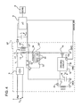
Figure 3 shows apower supply circuit 30, in particular a switch-mode power supply (SMPS) circuit of a flyback type. Elements of thepower supply circuit 30 ofFigure 3 , analogous to and having substantially the same function of the ones described with reference to thepower supply circuit 4 ofFigure 2 , will not be described any further herein. - The
power supply circuit 30 comprises a turn-on circuit 32 that can be activated remotely. - The turn-on circuit 32 comprises a turn-on
transistor 16 similar to the one described with reference toFigure 2 . However, in this case the gate terminal G of the turn-ontransistor 16 is not directly connected to, and controlled by, thedriving circuit 19. - The turn-on circuit 32, which can be connected indifferently to the first terminal 12' or to the
second terminal 12", further comprises atransducer 33, which can be remote-controlled and is configured to enable, when activated, passage of a current through it. Thetransducer 33 is connected between the drain terminal D of the turn-ontransistor 16 and the gate terminal G of the turn-ontransistor 16. - The
transducer 33 can be a photodiode, a photomultiplier or a phototransistor, configured so as to enable passage of a current across its terminals if activated by a light beam at a particular wavelength or within a range of wavelengths. Furthermore, thetransducer 33 can be formed by a plurality of photodiodes or photomultipliers or phototransistors connected in series one another. - Finally, the turn-on circuit 32 comprises a turn-
off resistor 34, preferably having a resistance comprised between 100 kΩ and 2 MΩ, connected between the gate terminal G of the turn-ontransistor 16 and the source terminal S of the turn-ontransistor 16; and aZener diode 35, connected between the gate terminal G of the turn-ontransistor 16 and the source terminal S of the turn-ontransistor 16, in parallel to the turn-off resistor 34, and having a Zener voltage VZENER preferably of 30 V. - For simplicity of description, in what follows reference will be made to a
transducer 33 of an optical/electrical type, more precisely aphototransistor 36. Thephototransistor 36 is activated by means of an incident light beam, preferably not visible by the human eye and having, for example, a wavelength in the infrared (greater than 700 nm) or in the ultraviolet (less than 400 nm). The light beam may be generated by a user through a remote control (shown in) configured for generating such a light beam. - In use, when the
phototransistor 36 is driven in conduction (by means of an incident light beam having, for example, a wavelength in the infrared), a current flows through it and a voltage develops across its terminals, biasing the gate terminal G of the turn-ontransistor 16. If the biasing voltage generated is higher than the conduction threshold of the turn-ontransistor 16, the turn-ontransistor 16 turns on, connecting thesupply port 2 with the turn-oncapacitor 18, through therectifier 9 and the primary winding 12 of thetransformer 11. In this way, the turn-oncapacitor 18 is charged and, when the voltage on the turn-oncapacitor 18 reaches a value VC sufficient to supply the drivingcircuit 19, the drivingcircuit 19 turns on and drives in conduction the switchingtransistor 15. Hence, the drivingcircuit 19 is supplied by the auxiliary winding 21. - In order to guarantee turning-on of the driving
circuit 19, it is expedient for the turn-ontransistor 16 to be driven in conduction by the phototransistor 36 (which, in turn, is driven in conduction by the incident light beam generated by the user) for a time sufficient to charge the turn-oncapacitor 18. When a voltage VC, sufficient to supply the drivingcircuit 19, establishes on the turn-oncapacitor 18, the drivingcircuit 19 switches on. - The current that the
phototransistor 36 must generate, when it is activated by the incident light beam, is not very high. In particular, in the case of use of a turn-ontransistor 16 having a gate capacitance of few nF (nanofarads), it is sufficient for thephototransistor 36 to generate a few tens of µA (microampere). In this case, the supply voltage VC of the drivingcircuit 19 is reached in a time of the order of a few hundreds of milliseconds, practically negligible for human perception. - The turn-
off resistor 34 has the function of draining a possible leakage current of thephototransistor 36, for example caused by undesirable components of a light signal (e.g., natural light) accidentally incident on thephototransistor 36. Moreover, the turn-off resistor 34 favours the switching-off (interdiction state) of the turn-ontransistor 16, draining the charge possibly accumulated on the gate terminal G of the turn-ontransistor 16 during its operative state. TheZener diode 35 has the function of limiting the potential applied to the gate terminal G of the turn-ontransistor 16 to a maximum value represented by the Zener voltage VZENER, proper to theZener diode 35. In this way, saturation in conduction of the turn-ontransistor 16 is prevented. - After the turning-on step, the driving
circuit 19 controls in conduction the switchingtransistor 15. In this way, a current flows through the primary winding 12 of thetransformer 11 and supplies, via the auxiliary winding 21, the drivingcircuit 19 itself. In use, the switchingtransistor 15 can be controlled via a square-wave modulation (pulse-width modulation - PWM) signal with variable frequency, usually higher than 16 kHz, and enables transfer onto the secondary winding 24 of the supply for operation of themicrocontroller 5. - Turning-off of the
power supply circuit 30 can be advantageously managed by themicrocontroller 5. For example, drivingcircuits 19 are known provided with a turn-offinput 19a. In this case, themicrocontroller 5 is connected to said turn-offinput 19a for turning-off the drivingcircuit 19 through a signal Driver_OFF, and consequently turning off thepower supply circuit 30. In fact, in the absence of an appropriate light beam incident on the active area of thephototransistor 36, the turn-ontransistor 16 is controlled in interdiction, and, after turning-off of the drivingcircuit 19, also the switchingtransistor 15 is controlled in interdiction. Consequently, in the absence of supply, thepower supply circuit 30 turns off. - As an alternative to the turning-off command by means of the signal Driver_OFF managed by the
microcontroller 5, there can be provided an appropriate circuit (not illustrated) for discharging of the turn-oncapacitor 18 and for interrupting the supply of the drivingcircuit 19 managed by themicrocontroller 5. Or, yet again, themicrocontroller 5 could drive in interdiction the switchingtransistor 15, interrupting the flow of current through the primary winding 12 of thetransformer 11. - The
power supply circuit 30 can be supplied by a mains supply, such as domestic power, or by a battery. In the case of battery supply, however, thepower supply circuit 30 does not require therectifier 9. - Finally, a main switch of the electrical appliance in which the
power supply circuit 30 is implemented (analogous to thesupply switch 8 illustrated inFigure 2 ), connected between thesupply port 2 and thetransformer 11, is not necessary. In fact, in the off state of the power supply circuit 30 (i.e., in the state in which thepower supply circuit 30 does not provide electrical supply), the turn-ontransistor 16, the switchingtransistor 15, and thetransducer 33 are interdicted and do not conduct any current. Thepower supply circuit 30 performs itself the function of main switch of the electrical appliance in which it operates. -
Figure 4 shows a power supply circuit 30' according to a further embodiment of the present disclosure. Elements of the power supply circuit 30' ofFigure 4 analogous to and having substantially the same function of elements described with reference to thepower supply circuit 30 ofFigure 3 are not further described herein. - In the embodiment of
Figure 4 , the power supply circuit 30' comprises a turn-on circuit 32' that can be activated remotely, as already explained with reference toFigure 3 . The turn-on circuit 32' can be connected indifferently to the first terminal 12' or to thesecond terminal 12" (Figure 4 shows the turn-on circuit 32' connected to thesecond terminal 12") and comprises the turn-ontransistor 16, thetransducer 33 and the turn-off resistor 34. However, unlike the embodiment ofFigure 3 , thesecond terminal 12" of the primary winding 12 is connected in series to a source terminal S of the turn-ontransistor 16. The turn-ontransistor 16 is connected, through an own drain terminal D, to the turn-oncapacitor 18, which is in turn connected to a ground reference voltage GND. The turn-off resistor 34 is connected in parallel to thetransducer 33, i.e. one of its terminal is connected to the gate of the turn-ontransistor 16 and the other terminal is connected to the source terminal S of the turn-on transistor 16 (which corresponds, inFigure 4 , to thesecond terminal 12"). - The
transducer 33 is remote-controlled and is configured to enable, when activated, passage of a current through it. Thetransducer 33 is connected between the source terminal S of the turn-ontransistor 16 and the gate terminal G of the turn-ontransistor 16. Thetransducer 33 according to the embodiment ofFigure 4 is formed by a plurality of photodiodes connected in series one another. However, a single photodiode may be used, provided that, during activation, it generates across its terminals a voltage sufficiently high to control in conduction the turn-ontransistor 16. For example, in case the turn-ontransistor 16 is a MOSFET device, the voltage is sufficiently high when the gate terminal G of theMOSFET device 16 is polarized above the MOSFET threshold voltage value for conduction channel formation. - The
transducer 33 ofFigure 4 may be activated by means of an incident light beam (generated by a user through a remote control) preferably in the infrared range. As known, a photodiode is configured to generate, when illuminated, current carriers (electrons/holes). In particular, the current carrier generation causes a direct polarization of eachphotodiode 40, which develops across its terminals a voltage higher than its conduction threshold voltage, for example a voltage of about 600-700 mV. In this way, during use, the current through thephotodiodes 40 is almost completely due to the incident light beam, and proportional to the incident light intensity. In absence of incident light beam, eachphotodiode 40 develops a voltage across its terminals which is lower than its conduction threshold voltage (and current substantially equal to zero). -
Figure 5 shows apower supply circuit 30" according to a further embodiment of the present disclosure. Elements of thepower supply circuit 30" ofFigure 5 analogous to and having substantially the same function of elements described with reference to thepower supply circuit 30 ofFigure 3 or power supply circuit 30' ofFigure 4 are not further described herein. - According to the embodiment of
Figure 5 , thetransducer 33 is connected in the same way as already described with reference toFigure 4 . However, thetransducer 33 comprises an antenna 44 (e.g., a patch antenna) connected between the source S and gate G terminals of the turn-ontransistor 16. When no activation signal is provided to theantenna 44, the source S and gate G terminals of the turn-ontransistor 16 are shortcircuited and thus the turn-ontransistor 16 is off (i.e., it has an open circuit behaviour and no current flows through it). However, when an electromagnetic signal (generated by a user through a remote control) is provided to theantenna 44 so as to induce a current flow through theantenna 44, a voltage develops between the source S and gate G terminals of the turn-ontransistor 16. By configuring the antenna 44 (e.g., by providing a sufficient number of turns) so that the voltage developed across theantenna 44 is higher that the conduction threshold voltage of the turn-ontransistor 16, for example a voltage of about 600-700 mV, it is possible to control in an on-state the turn-ontransistor 16. - The advantage of the embodiments of
Figures 4 andFigure 5 , with respect to the embodiment ofFigure 3 , is that high voltage structures are not used. -
Figure 6 shows a block diagram of asystem 50 comprising anelectrical appliance 49 and aremote control 57. By means of theremote control 57, theelectrical appliance 49 can be remotely controlled for being turned on and turned off. Theelectrical appliance 49 may, for example, be an audio/video system such as a television set, a hi-fi system, a video recorder, or an electrical household appliance in general, which implements thepower supply circuit 30. In particular, theremote control 57 is configured for issuing a command (i.e., an appropriate wireless signal) for remote activation of thetransducer 33 of thepower supply circuit 30, in order to manage turning-on of theelectrical appliance 49. The remote activation command can be generated by pressing an appropriate key, present on theremote control 57, which governs generation of the appropriate activation wireless signal. Such a wireless signal is, according with the described embodiment, a light beam having a wavelength and a power configured so as to control thephototransistor 36 in generation of an electrical current. - In some electrical devices of a known type, for example in some television sets, two supply circuits are present: a main power supply circuit, which supplies the electrical appliance as a whole during normal use (usually, for safety reasons, obtained with insulated topologies for example of a flyback type, forward type, resonant type, etc.) and an auxiliary power supply circuit, used in the step of turning-on of the electrical appliance and in stand-by mode. Separate implementation of the main power supply circuit and of the auxiliary power supply circuit guarantees a better energy efficiency, but at a higher cost. The turn-on circuit 32 according to the present invention can be implemented indifferently in a main power supply circuit or in an auxiliary power supply circuit. However, by implementing the turn-on circuit 32 according to the present invention in a main power supply circuit a high energy efficiency, a high level of integration of the components, and reduced production costs are guaranteed simultaneously.
- The
electrical appliance 49 ofFigure 6 is supplied by means of a mainpower supply circuit 30 connected to thesupply port 2, which is, in turn, connected, for example, to the mains supply (e.g., household power line). Theelectrical appliance 49 comprises: themicrocontroller 5, which is connected to thepower supply circuit 30 from which it receives the supply, and communicates with thecommand sensor 6; a sound-reproducingcircuit 51, which is connected to thepower supply circuit 30 from which it receives the supply, and communicates with themicrocontroller 5 and with one ormore loudspeakers 55; optionally amemory 52, which is connected to thepower supply circuit 30 from which it receives the supply, and communicates with themicrocontroller 5, for storing possible programming information of theelectronic appliance 49; and, optionally, a video-reproducingcircuit 53, which is connected to thepower supply circuit 30 from which it receives the supply, and communicates with themicrocontroller 5 and is configured for managing display of graphic information or images on adisplay 54. The sound-reproducingcircuit 51, thememory 52, the video-reproducingcircuit 53, thedisplay 54, and theloudspeakers 55 can be supplied by means of respective secondary windings (not illustrated) of thetransformer 11 of thepower supply circuit 30 ofFigure 3 . - From an examination of the characteristics of the switch-mode power supply circuit provided according to the present invention the advantages that it makes possible are evident.
- In particular, it is possible to eliminate the electric-power consumption of electrical or electronic appliances in stand-by mode, without loosing the convenience of turning-on via remote control of the electrical or electronic appliance itself.
- Furthermore, the time necessary for turning-on is of the order of a few hundreds of milliseconds, practically negligible for human perception.
- Finally, it is clear that modifications and variations may be made to the switch-mode power supply circuit described and illustrated herein, without thereby departing from the sphere of protection of the present invention, as defined in the annexed claims.
- For example, in order to limit the sensitivity of a transducer of an optical type (for example, a phototransistor) at a particular wavelength or within a range of wavelengths, it may prove advantageous to set an appropriate filter external to the phototransistor, configured so as to enable passage exclusively of the wavelength/wavelengths of interest.
- Furthermore, according to the maximum voltage that the phototransistor sustains (depending upon the supply voltage VAL), it may be expedient to connect a plurality of
phototransistors 36 in series to one another. - In addition, the turn-on
transistor 16 and the switchingtransistor 15 can be different from a MOSFET transistor; for example, they can be IGBT (insulated-gate bipolar transistor) devices or generic electronic switches. - Finally, the
transducer 33 can be of a different type from what has been described. For example, it can be of an electromagnetic type, comprising an antenna and can be remotely activated by means of an electromagnetic signal.
Claims (18)
- A power supply circuit (30; 30'; 30") for an electrical appliance (49), comprising a turning-on stage (32; 32') configured for triggering a transition from a turned-off state, wherein said power supply circuit (30; 30'; 30") is off and does not supply electric power, to a turned-on state of said power supply circuit (30; 30'; 30"), said turning-on stage (32; 32') comprising a transducer (33; 36; 40; 44), of a remote-controlled type, configured for triggering said transition in response to a reception of a wireless signal,
said turning-on stage (32; 32') comprises a turn-on transistor (16) coupled to said transducer (33; 36; 40; 44), the transducer (33; 36; 40; 44) switching on the turn-on transistor (16) in response to the reception of the wireless signal,
characterized in that the power supply circuit further comprises:a supply input (2) and a reference voltage terminal (GND) ;a charge-storage element (18) coupled between the reference voltage terminal (GND) and the turn-on transistor (16) so that, when the turn-on transistor (16) is switched-on, the charge-storage element (18) is charged by the first supply input (2), the turn-on transistor (16) comprising a gate terminal (G) connected to the transducer (33; 36; 40; 44);a triggering switch (15), coupled between the supply input (2) and the reference voltage terminal (GND); anda driving circuit (19), having a supply input coupled to the charge-storage element (18) and a control output coupled to a control terminal (G) of the triggering switch (15),whereby the charge-storage element (18) develops, when charged, a supply voltage (VC) adapted to turn on the driving circuit (19), andwhereby the driving circuit (19) is configured to switch on the triggering switch (15) thus connecting the supply input (2) to the reference voltage terminal (GND) and powering the power supply circuit. - The power supply circuit according to claim 1, wherein the turn-on transistor (16) has a first conduction terminal (S; D) connected to the supply input (2), a second conduction terminal (D; S) connected to the charge storage element (18), and a control terminal (G), said transducer (33; 36; 40; 44) being connected between the control terminal (G) and the first conduction terminal (S; D) of the turn-on transistor (16) and being configured to switch-on said turn-on transistor (16) thereby connecting the supply input (2) with the charge-storage element (18).
- The power supply circuit according to claim 2, wherein said turning-on stage (32; 32') further comprises a resistor (34), having a first conduction terminal connected to the control terminal (G) of the turn-on transistor (16) and a second conduction terminal connected to the second conduction terminal (S) of the turn-on transistor (16).
- The power supply circuit according to claim 2 or claim 3, wherein said turning-on stage (32; 32') further comprises a Zener diode (35), having a first conduction terminal connected to the control terminal (G) of the turn-on transistor (16) and a second conduction terminal connected to the second conduction terminal (S) of the turn-on transistor (16).
- The power supply circuit according to claim 2, wherein said turning-on stage (32; 32') further comprises a resistor (34), having a first conduction terminal connected to the control terminal (G) of the turn-on transistor (16) and a second conduction terminal connected to the first conduction terminal (S) of the turn-on transistor (16).
- The power supply circuit according to any one of the previous claims, wherein the transducer (33; 36; 40; 44) comprises an antenna.
- The power supply circuit according to any one of the claims 1-5, wherein the transducer (33; 36; 40; 44) is an optoelectronic device.
- The power supply circuit according to claim 7, wherein the transducer (33; 36; 40; 44) comprises at least one phototransistor (36).
- The power supply circuit according to claim 7, wherein the transducer (33; 36; 40; 44) comprises at least one photodiode (40).
- The power supply circuit according to claim 9, wherein the transducer (33; 36; 40; 44) comprises at least another photodiode (40) connected in series to the at least one photodiode (40).
- The power supply circuit according to any one of the previous claims, wherein the transducer (33; 36; 40; 44) is configured for triggering said transition in response to the reception of a wireless signal of electromagnetic type.
- The power supply circuit according to any one of the preceding claims, said power supply circuit (30; 30'; 30") being of a switching type and further comprising a transformer (11) having a primary winding (12) coupled between the supply input (2) of the power supply circuit and the reference voltage terminal (GND) through the triggering switch (15), and at least a secondary winding (24) coupled to an output of the power supply circuit,
and wherein the driving circuit (19) further comprises a control port (19a) configured for receiving a turning-off signal (Driver_OFF) to switch off the triggering switch (15) and turn off the power supply circuit (30; 30'; 30"). - An electrical appliance (49) comprising a power supply circuit (30; 30'; 30") according to any one of claims 1-12.
- The electrical appliance according to claim 13, further comprising a microcontroller (5), coupled to an output of said power supply circuit (30; 30'; 30") and having a switching-off output connected to said power supply circuit (30; 30'; 30").
- The electrical appliance according to claim 12 or claim 14, wherein said electrical appliance is chosen in the group comprising: a television set, a hi-fi equipment, a video recorder, an electrical household appliance.
- A turning-on system (50) comprising a power supply circuit according to any one of claims 1-12 and a remote control (57), wherein said remote control (57) is configured so as to generate said wireless signal.
- A method of supplying an electrical appliance (49), comprising a step of turning-on a power supply circuit (30; 30'; 30") from a turned-off state, in which the power supply circuit (30; 30'; 30") is operatively disconnected from a first and a second supply inputs (2, GND), to a turned-on state, in which the power supply circuit (30; 30'; 30") is operatively connected to the first and the second supply inputs (2, GND), said turning-on step comprises the steps of:receiving a wireless signal by means of a transducer (33; 36) of a remote-controlled type;switching on the transducer (33; 36) in response to the wireless signal developing, across output conduction terminals of the transducer, an output voltage which is a function of the wireless signal received; andswitching on, by said output voltage, a turn-on transistor (16),characterized in that the turning-on step further comprises the steps of:charging a charge-storage element (18) through the turn-on transistor (16), which comprises a gate terminal (G) being connected to the transducer (33;36);develop, by the charge-storage element (18), a supply voltage (VC) adapted to turn on the driving circuit (19),whereby the power supply circuit further comprises a triggering switch (15), coupled between the supply input (2) and a reference voltage terminal (GND), and a driving circuit (19), having a supply input coupled to the charge-storage element (18) and a control output coupled to a control terminal (G) of the triggering switch (15), the method further comprising the steps of:switching on, by the driving circuit (19), the triggering switch (15) thus connecting the supply input (2) to the reference voltage terminal (GND); andsupplying the power supply circuit through the first and second supply inputs (2, GND).
- The method according to claim 17, wherein the step of receiving a wireless signal comprises receiving an electromagnetic signal.
Applications Claiming Priority (2)
| Application Number | Priority Date | Filing Date | Title |
|---|---|---|---|
| IT000214A ITTO20090214A1 (en) | 2009-03-20 | 2009-03-20 | POWER CIRCUIT FOR REMOTE IGNITION OF ELECTRIC APPLIANCES |
| PCT/EP2010/053480 WO2010106113A2 (en) | 2009-03-20 | 2010-03-17 | Power supply circuit for remotely turning-on electrical appliances |
Publications (2)
| Publication Number | Publication Date |
|---|---|
| EP2409392A2 EP2409392A2 (en) | 2012-01-25 |
| EP2409392B1 true EP2409392B1 (en) | 2015-07-22 |
Family
ID=41226209
Family Applications (1)
| Application Number | Title | Priority Date | Filing Date |
|---|---|---|---|
| EP10710014.1A Active EP2409392B1 (en) | 2009-03-20 | 2010-03-17 | Power supply circuit for remotely turning-on electrical appliances |
Country Status (4)
| Country | Link |
|---|---|
| US (1) | US8933592B2 (en) |
| EP (1) | EP2409392B1 (en) |
| IT (1) | ITTO20090214A1 (en) |
| WO (1) | WO2010106113A2 (en) |
Families Citing this family (15)
| Publication number | Priority date | Publication date | Assignee | Title |
|---|---|---|---|---|
| DE102011077660A1 (en) * | 2011-06-16 | 2012-12-20 | Meiko Maschinenbau Gmbh & Co. Kg | Cleaning device with energy storage |
| FR2977119B1 (en) * | 2011-06-24 | 2017-06-16 | Valeo Japan Co Ltd | PRINTED CIRCUIT BOARD FOR COMPRESSOR HOUSING |
| CN103051317A (en) * | 2011-10-14 | 2013-04-17 | 成都锐奕信息技术有限公司 | On-off switch circuit triggered by wireless signal |
| US9496793B2 (en) * | 2011-11-01 | 2016-11-15 | Azoteq (Pty) Ltd | Capacitive sensing enabled switch mode power supply and data transfer |
| JP5360270B2 (en) * | 2011-12-07 | 2013-12-04 | 凸版印刷株式会社 | Liquid crystal display |
| ITMI20121436A1 (en) * | 2012-08-21 | 2014-02-22 | St Microelectronics Srl | POWER SUPPLY FOR AN ELECTRIC APPLIANCE. |
| US9461534B2 (en) | 2012-08-21 | 2016-10-04 | Stmicroelectronics S.R.L. | Wirelessly activated power supply for an electronic device |
| US9305907B2 (en) | 2013-03-22 | 2016-04-05 | Stmicroelectronics S.R.L. | Optoelectronic integrated device including a photodetector and a MOSFET transistor, and manufacturing process thereof |
| CN103885345A (en) * | 2013-09-09 | 2014-06-25 | 苏州将鹏五金有限公司 | Remote-control-type power supply management device and management method thereof |
| US9236909B2 (en) | 2013-12-19 | 2016-01-12 | Stmicroelectronics, Inc. | Zero standby power for powerline communication devices |
| CN103869718A (en) * | 2014-02-25 | 2014-06-18 | 朱金荣 | System device for realizing zero power consumption standby of household appliance |
| CN104678851B (en) | 2015-01-29 | 2018-03-16 | 小米科技有限责任公司 | Smart jack method of controlling switch and device |
| CN104898514B (en) * | 2015-05-06 | 2017-12-26 | 泰康保险集团股份有限公司 | Intelligent power, control method and control system |
| DE102017209734B4 (en) | 2017-06-09 | 2019-03-07 | Ifm Electronic Gmbh | Battery operated electronic switching device with a standby mode |
| IT201900006609A1 (en) | 2019-05-07 | 2020-11-07 | St Microelectronics Srl | OPERATING PROCEDURE OF A RADIO TRANSMITTER AND CORRESPONDING RADIO TRANSMITTER |
Family Cites Families (14)
| Publication number | Priority date | Publication date | Assignee | Title |
|---|---|---|---|---|
| US4500923A (en) * | 1982-10-29 | 1985-02-19 | Rca Corporation | Television receiver standby power supply |
| US4651214A (en) * | 1984-12-24 | 1987-03-17 | Rca Corporation | Remote controlled television receiver power supply |
| US4751580A (en) * | 1985-12-19 | 1988-06-14 | Rca Licensing Corporation | Television receiver standby power supply |
| US5014178A (en) | 1990-05-14 | 1991-05-07 | Power Integrations, Inc. | Self powering technique for integrated switched mode power supply |
| DE4237634A1 (en) * | 1992-11-07 | 1994-05-11 | Nokia Deutschland Gmbh | Video receiving device with a switching power supply |
| DE4321948C3 (en) * | 1993-07-01 | 1999-02-25 | Siemens Ag | Standby circuit for electrical consumers |
| JPH07123709A (en) * | 1993-10-28 | 1995-05-12 | Matsushita Electric Ind Co Ltd | Power unit |
| TW432276B (en) * | 1997-03-08 | 2001-05-01 | Acer Peripherals Inc | Power-saving type power-supply with the capability of quickly restoring the start |
| KR100438695B1 (en) | 2001-03-09 | 2004-07-05 | 삼성전자주식회사 | Apparatus for controlling power supply and method thereof |
| JP4682647B2 (en) * | 2005-03-07 | 2011-05-11 | サンケン電気株式会社 | Switching power supply |
| GB2436979B (en) * | 2007-05-09 | 2008-04-02 | Andrew James Stanford-Clark | Standby power consumption limiting device |
| KR100935186B1 (en) * | 2007-06-27 | 2010-01-06 | 임성규 | Plug apparatus |
| US20110001887A1 (en) | 2009-07-02 | 2011-01-06 | Peter Rae Shintani | Zero standby power RF controlled device |
| US20110001651A1 (en) | 2009-07-02 | 2011-01-06 | Candelore Brant L | Zero standby power laser controlled device |
-
2009
- 2009-03-20 IT IT000214A patent/ITTO20090214A1/en unknown
-
2010
- 2010-03-17 EP EP10710014.1A patent/EP2409392B1/en active Active
- 2010-03-17 WO PCT/EP2010/053480 patent/WO2010106113A2/en active Application Filing
- 2010-03-17 US US13/256,913 patent/US8933592B2/en active Active
Also Published As
| Publication number | Publication date |
|---|---|
| ITTO20090214A1 (en) | 2010-09-21 |
| EP2409392A2 (en) | 2012-01-25 |
| US20120057379A1 (en) | 2012-03-08 |
| WO2010106113A2 (en) | 2010-09-23 |
| US8933592B2 (en) | 2015-01-13 |
| WO2010106113A3 (en) | 2011-03-31 |
Similar Documents
| Publication | Publication Date | Title |
|---|---|---|
| EP2409392B1 (en) | Power supply circuit for remotely turning-on electrical appliances | |
| US9118250B2 (en) | Power supply circuit for remotely turning-on electrical appliances | |
| KR100376131B1 (en) | Consumption power saving apparatus and controlling method in a stand-by mode | |
| US10063091B2 (en) | Standby power saving circuit | |
| CN105406717A (en) | LLC converter and loss of inductive mode detection circuit | |
| WO2011002062A1 (en) | Power-supply control device, power supply system, and electronic device | |
| CN108631601B (en) | Multi-input converter | |
| US9673714B2 (en) | Power supply apparatus for an electrical appliance | |
| CN103731031A (en) | Power source and power source voltage regulating method | |
| US6297601B1 (en) | Apparatus and method for saving electric power in a display system | |
| US10658922B2 (en) | Control circuit and display apparatus for reduced standby power consumption | |
| US10536088B2 (en) | Switched mode power supply controller | |
| La Rosa et al. | An innovative system capable to turn on any turned off electrical appliance by means of an efficient optical energy transfer | |
| US9461534B2 (en) | Wirelessly activated power supply for an electronic device | |
| KR20100127769A (en) | A switchable load for initializing an output voltage of a power supply | |
| EP2892135B1 (en) | Power Supply and energy efficient Gate Driver | |
| KR102439266B1 (en) | Low-power smart remote control using capacitors and solar panels | |
| CN101437126A (en) | Power supply control method, circuit and television set | |
| KR101728740B1 (en) | Power supply controlling apparatus of electrical instrument and method for controlling the same | |
| JP4086051B2 (en) | OPTICAL COMMUNICATION APPARATUS, USE METHOD THEREOF, OPTICAL COMMUNICATION SYSTEM | |
| CN220067227U (en) | BUCK circuit, power conversion device and household appliance | |
| US11923757B2 (en) | Electronic device for cutting off power | |
| KR102207800B1 (en) | Electronic device for cutting off power | |
| CN110505738B (en) | Intelligent control system for adjusting lamp brightness according to switching time interval | |
| CN109994924B (en) | Solid-state light source driving device and projection apparatus |
Legal Events
| Date | Code | Title | Description |
|---|---|---|---|
| PUAI | Public reference made under article 153(3) epc to a published international application that has entered the european phase |
Free format text: ORIGINAL CODE: 0009012 |
|
| 17P | Request for examination filed |
Effective date: 20111020 |
|
| AK | Designated contracting states |
Kind code of ref document: A2 Designated state(s): AT BE BG CH CY CZ DE DK EE ES FI FR GB GR HR HU IE IS IT LI LT LU LV MC MK MT NL NO PL PT RO SE SI SK SM TR |
|
| RAP1 | Party data changed (applicant data changed or rights of an application transferred) |
Owner name: STMICROELECTRONICS SRL |
|
| DAX | Request for extension of the european patent (deleted) | ||
| 17Q | First examination report despatched |
Effective date: 20140423 |
|
| GRAP | Despatch of communication of intention to grant a patent |
Free format text: ORIGINAL CODE: EPIDOSNIGR1 |
|
| INTG | Intention to grant announced |
Effective date: 20150210 |
|
| GRAS | Grant fee paid |
Free format text: ORIGINAL CODE: EPIDOSNIGR3 |
|
| GRAA | (expected) grant |
Free format text: ORIGINAL CODE: 0009210 |
|
| AK | Designated contracting states |
Kind code of ref document: B1 Designated state(s): AT BE BG CH CY CZ DE DK EE ES FI FR GB GR HR HU IE IS IT LI LT LU LV MC MK MT NL NO PL PT RO SE SI SK SM TR |
|
| REG | Reference to a national code |
Ref country code: GB Ref legal event code: FG4D |
|
| REG | Reference to a national code |
Ref country code: CH Ref legal event code: EP |
|
| REG | Reference to a national code |
Ref country code: IE Ref legal event code: FG4D |
|
| REG | Reference to a national code |
Ref country code: AT Ref legal event code: REF Ref document number: 738378 Country of ref document: AT Kind code of ref document: T Effective date: 20150815 |
|
| REG | Reference to a national code |
Ref country code: DE Ref legal event code: R096 Ref document number: 602010026030 Country of ref document: DE |
|
| REG | Reference to a national code |
Ref country code: AT Ref legal event code: MK05 Ref document number: 738378 Country of ref document: AT Kind code of ref document: T Effective date: 20150722 |
|
| REG | Reference to a national code |
Ref country code: LT Ref legal event code: MG4D |
|
| REG | Reference to a national code |
Ref country code: NL Ref legal event code: MP Effective date: 20150722 |
|
| PG25 | Lapsed in a contracting state [announced via postgrant information from national office to epo] |
Ref country code: LT Free format text: LAPSE BECAUSE OF FAILURE TO SUBMIT A TRANSLATION OF THE DESCRIPTION OR TO PAY THE FEE WITHIN THE PRESCRIBED TIME-LIMIT Effective date: 20150722 Ref country code: LV Free format text: LAPSE BECAUSE OF FAILURE TO SUBMIT A TRANSLATION OF THE DESCRIPTION OR TO PAY THE FEE WITHIN THE PRESCRIBED TIME-LIMIT Effective date: 20150722 Ref country code: FI Free format text: LAPSE BECAUSE OF FAILURE TO SUBMIT A TRANSLATION OF THE DESCRIPTION OR TO PAY THE FEE WITHIN THE PRESCRIBED TIME-LIMIT Effective date: 20150722 Ref country code: NO Free format text: LAPSE BECAUSE OF FAILURE TO SUBMIT A TRANSLATION OF THE DESCRIPTION OR TO PAY THE FEE WITHIN THE PRESCRIBED TIME-LIMIT Effective date: 20151022 Ref country code: GR Free format text: LAPSE BECAUSE OF FAILURE TO SUBMIT A TRANSLATION OF THE DESCRIPTION OR TO PAY THE FEE WITHIN THE PRESCRIBED TIME-LIMIT Effective date: 20151023 |
|
| REG | Reference to a national code |
Ref country code: FR Ref legal event code: PLFP Year of fee payment: 7 |
|
| PG25 | Lapsed in a contracting state [announced via postgrant information from national office to epo] |
Ref country code: PL Free format text: LAPSE BECAUSE OF FAILURE TO SUBMIT A TRANSLATION OF THE DESCRIPTION OR TO PAY THE FEE WITHIN THE PRESCRIBED TIME-LIMIT Effective date: 20150722 Ref country code: AT Free format text: LAPSE BECAUSE OF FAILURE TO SUBMIT A TRANSLATION OF THE DESCRIPTION OR TO PAY THE FEE WITHIN THE PRESCRIBED TIME-LIMIT Effective date: 20150722 Ref country code: SE Free format text: LAPSE BECAUSE OF FAILURE TO SUBMIT A TRANSLATION OF THE DESCRIPTION OR TO PAY THE FEE WITHIN THE PRESCRIBED TIME-LIMIT Effective date: 20150722 Ref country code: ES Free format text: LAPSE BECAUSE OF FAILURE TO SUBMIT A TRANSLATION OF THE DESCRIPTION OR TO PAY THE FEE WITHIN THE PRESCRIBED TIME-LIMIT Effective date: 20150722 Ref country code: HR Free format text: LAPSE BECAUSE OF FAILURE TO SUBMIT A TRANSLATION OF THE DESCRIPTION OR TO PAY THE FEE WITHIN THE PRESCRIBED TIME-LIMIT Effective date: 20150722 Ref country code: PT Free format text: LAPSE BECAUSE OF FAILURE TO SUBMIT A TRANSLATION OF THE DESCRIPTION OR TO PAY THE FEE WITHIN THE PRESCRIBED TIME-LIMIT Effective date: 20151123 Ref country code: IS Free format text: LAPSE BECAUSE OF FAILURE TO SUBMIT A TRANSLATION OF THE DESCRIPTION OR TO PAY THE FEE WITHIN THE PRESCRIBED TIME-LIMIT Effective date: 20151122 |
|
| REG | Reference to a national code |
Ref country code: DE Ref legal event code: R097 Ref document number: 602010026030 Country of ref document: DE |
|
| PG25 | Lapsed in a contracting state [announced via postgrant information from national office to epo] |
Ref country code: SK Free format text: LAPSE BECAUSE OF FAILURE TO SUBMIT A TRANSLATION OF THE DESCRIPTION OR TO PAY THE FEE WITHIN THE PRESCRIBED TIME-LIMIT Effective date: 20150722 Ref country code: EE Free format text: LAPSE BECAUSE OF FAILURE TO SUBMIT A TRANSLATION OF THE DESCRIPTION OR TO PAY THE FEE WITHIN THE PRESCRIBED TIME-LIMIT Effective date: 20150722 Ref country code: CZ Free format text: LAPSE BECAUSE OF FAILURE TO SUBMIT A TRANSLATION OF THE DESCRIPTION OR TO PAY THE FEE WITHIN THE PRESCRIBED TIME-LIMIT Effective date: 20150722 Ref country code: DK Free format text: LAPSE BECAUSE OF FAILURE TO SUBMIT A TRANSLATION OF THE DESCRIPTION OR TO PAY THE FEE WITHIN THE PRESCRIBED TIME-LIMIT Effective date: 20150722 |
|
| PLBE | No opposition filed within time limit |
Free format text: ORIGINAL CODE: 0009261 |
|
| STAA | Information on the status of an ep patent application or granted ep patent |
Free format text: STATUS: NO OPPOSITION FILED WITHIN TIME LIMIT |
|
| PG25 | Lapsed in a contracting state [announced via postgrant information from national office to epo] |
Ref country code: RO Free format text: LAPSE BECAUSE OF FAILURE TO SUBMIT A TRANSLATION OF THE DESCRIPTION OR TO PAY THE FEE WITHIN THE PRESCRIBED TIME-LIMIT Effective date: 20150722 |
|
| 26N | No opposition filed |
Effective date: 20160425 |
|
| PG25 | Lapsed in a contracting state [announced via postgrant information from national office to epo] |
Ref country code: SI Free format text: LAPSE BECAUSE OF FAILURE TO SUBMIT A TRANSLATION OF THE DESCRIPTION OR TO PAY THE FEE WITHIN THE PRESCRIBED TIME-LIMIT Effective date: 20150722 Ref country code: BE Free format text: LAPSE BECAUSE OF NON-PAYMENT OF DUE FEES Effective date: 20160331 |
|
| PG25 | Lapsed in a contracting state [announced via postgrant information from national office to epo] |
Ref country code: LU Free format text: LAPSE BECAUSE OF FAILURE TO SUBMIT A TRANSLATION OF THE DESCRIPTION OR TO PAY THE FEE WITHIN THE PRESCRIBED TIME-LIMIT Effective date: 20160317 Ref country code: MC Free format text: LAPSE BECAUSE OF FAILURE TO SUBMIT A TRANSLATION OF THE DESCRIPTION OR TO PAY THE FEE WITHIN THE PRESCRIBED TIME-LIMIT Effective date: 20150722 |
|
| REG | Reference to a national code |
Ref country code: CH Ref legal event code: PL |
|
| GBPC | Gb: european patent ceased through non-payment of renewal fee |
Effective date: 20160317 |
|
| REG | Reference to a national code |
Ref country code: IE Ref legal event code: MM4A |
|
| PG25 | Lapsed in a contracting state [announced via postgrant information from national office to epo] |
Ref country code: BE Free format text: LAPSE BECAUSE OF FAILURE TO SUBMIT A TRANSLATION OF THE DESCRIPTION OR TO PAY THE FEE WITHIN THE PRESCRIBED TIME-LIMIT Effective date: 20150722 |
|
| PG25 | Lapsed in a contracting state [announced via postgrant information from national office to epo] |
Ref country code: CH Free format text: LAPSE BECAUSE OF NON-PAYMENT OF DUE FEES Effective date: 20160331 Ref country code: LI Free format text: LAPSE BECAUSE OF NON-PAYMENT OF DUE FEES Effective date: 20160331 Ref country code: IE Free format text: LAPSE BECAUSE OF NON-PAYMENT OF DUE FEES Effective date: 20160317 Ref country code: GB Free format text: LAPSE BECAUSE OF NON-PAYMENT OF DUE FEES Effective date: 20160317 |
|
| REG | Reference to a national code |
Ref country code: FR Ref legal event code: PLFP Year of fee payment: 8 |
|
| PG25 | Lapsed in a contracting state [announced via postgrant information from national office to epo] |
Ref country code: NL Free format text: LAPSE BECAUSE OF FAILURE TO SUBMIT A TRANSLATION OF THE DESCRIPTION OR TO PAY THE FEE WITHIN THE PRESCRIBED TIME-LIMIT Effective date: 20150722 |
|
| PG25 | Lapsed in a contracting state [announced via postgrant information from national office to epo] |
Ref country code: MT Free format text: LAPSE BECAUSE OF FAILURE TO SUBMIT A TRANSLATION OF THE DESCRIPTION OR TO PAY THE FEE WITHIN THE PRESCRIBED TIME-LIMIT Effective date: 20150722 |
|
| REG | Reference to a national code |
Ref country code: FR Ref legal event code: PLFP Year of fee payment: 9 |
|
| PG25 | Lapsed in a contracting state [announced via postgrant information from national office to epo] |
Ref country code: CY Free format text: LAPSE BECAUSE OF FAILURE TO SUBMIT A TRANSLATION OF THE DESCRIPTION OR TO PAY THE FEE WITHIN THE PRESCRIBED TIME-LIMIT Effective date: 20150722 Ref country code: SM Free format text: LAPSE BECAUSE OF FAILURE TO SUBMIT A TRANSLATION OF THE DESCRIPTION OR TO PAY THE FEE WITHIN THE PRESCRIBED TIME-LIMIT Effective date: 20150722 Ref country code: HU Free format text: LAPSE BECAUSE OF FAILURE TO SUBMIT A TRANSLATION OF THE DESCRIPTION OR TO PAY THE FEE WITHIN THE PRESCRIBED TIME-LIMIT; INVALID AB INITIO Effective date: 20100317 |
|
| PG25 | Lapsed in a contracting state [announced via postgrant information from national office to epo] |
Ref country code: MK Free format text: LAPSE BECAUSE OF FAILURE TO SUBMIT A TRANSLATION OF THE DESCRIPTION OR TO PAY THE FEE WITHIN THE PRESCRIBED TIME-LIMIT Effective date: 20150722 Ref country code: TR Free format text: LAPSE BECAUSE OF FAILURE TO SUBMIT A TRANSLATION OF THE DESCRIPTION OR TO PAY THE FEE WITHIN THE PRESCRIBED TIME-LIMIT Effective date: 20150722 Ref country code: MT Free format text: LAPSE BECAUSE OF FAILURE TO SUBMIT A TRANSLATION OF THE DESCRIPTION OR TO PAY THE FEE WITHIN THE PRESCRIBED TIME-LIMIT Effective date: 20160331 |
|
| PG25 | Lapsed in a contracting state [announced via postgrant information from national office to epo] |
Ref country code: BG Free format text: LAPSE BECAUSE OF FAILURE TO SUBMIT A TRANSLATION OF THE DESCRIPTION OR TO PAY THE FEE WITHIN THE PRESCRIBED TIME-LIMIT Effective date: 20150722 |
|
| PGFP | Annual fee paid to national office [announced via postgrant information from national office to epo] |
Ref country code: IT Payment date: 20200218 Year of fee payment: 11 |
|
| PGFP | Annual fee paid to national office [announced via postgrant information from national office to epo] |
Ref country code: FR Payment date: 20200220 Year of fee payment: 11 |
|
| PG25 | Lapsed in a contracting state [announced via postgrant information from national office to epo] |
Ref country code: FR Free format text: LAPSE BECAUSE OF NON-PAYMENT OF DUE FEES Effective date: 20210331 |
|
| PG25 | Lapsed in a contracting state [announced via postgrant information from national office to epo] |
Ref country code: IT Free format text: LAPSE BECAUSE OF NON-PAYMENT OF DUE FEES Effective date: 20210317 |
|
| PGFP | Annual fee paid to national office [announced via postgrant information from national office to epo] |
Ref country code: DE Payment date: 20230221 Year of fee payment: 14 |