EP2409219B1 - Mechanismus zur schnellen detektion von overshift in einer floating-point-einheit - Google Patents
Mechanismus zur schnellen detektion von overshift in einer floating-point-einheit Download PDFInfo
- Publication number
- EP2409219B1 EP2409219B1 EP10710952.2A EP10710952A EP2409219B1 EP 2409219 B1 EP2409219 B1 EP 2409219B1 EP 10710952 A EP10710952 A EP 10710952A EP 2409219 B1 EP2409219 B1 EP 2409219B1
- Authority
- EP
- European Patent Office
- Prior art keywords
- overshift
- mantissa
- unit
- floating point
- value
- Prior art date
- Legal status (The legal status is an assumption and is not a legal conclusion. Google has not performed a legal analysis and makes no representation as to the accuracy of the status listed.)
- Active
Links
- 238000001514 detection method Methods 0.000 title description 12
- 230000007246 mechanism Effects 0.000 title description 4
- 230000004044 response Effects 0.000 claims description 5
- 238000010586 diagram Methods 0.000 description 8
- 230000001934 delay Effects 0.000 description 5
- 238000012986 modification Methods 0.000 description 4
- 230000004048 modification Effects 0.000 description 4
- 238000010606 normalization Methods 0.000 description 4
- 238000004364 calculation method Methods 0.000 description 3
- 238000013519 translation Methods 0.000 description 3
- 238000006073 displacement reaction Methods 0.000 description 2
- 238000000034 method Methods 0.000 description 2
- 230000008901 benefit Effects 0.000 description 1
- 230000002457 bidirectional effect Effects 0.000 description 1
- 230000001419 dependent effect Effects 0.000 description 1
- 238000013461 design Methods 0.000 description 1
- 230000000694 effects Effects 0.000 description 1
- 230000006870 function Effects 0.000 description 1
- 229910000078 germane Inorganic materials 0.000 description 1
- 238000012545 processing Methods 0.000 description 1
- 238000011084 recovery Methods 0.000 description 1
Images


Classifications
-
- G—PHYSICS
- G06—COMPUTING; CALCULATING OR COUNTING
- G06F—ELECTRIC DIGITAL DATA PROCESSING
- G06F5/00—Methods or arrangements for data conversion without changing the order or content of the data handled
- G06F5/01—Methods or arrangements for data conversion without changing the order or content of the data handled for shifting, e.g. justifying, scaling, normalising
- G06F5/012—Methods or arrangements for data conversion without changing the order or content of the data handled for shifting, e.g. justifying, scaling, normalising in floating-point computations
-
- G—PHYSICS
- G06—COMPUTING; CALCULATING OR COUNTING
- G06F—ELECTRIC DIGITAL DATA PROCESSING
- G06F7/00—Methods or arrangements for processing data by operating upon the order or content of the data handled
- G06F7/38—Methods or arrangements for performing computations using exclusively denominational number representation, e.g. using binary, ternary, decimal representation
- G06F7/48—Methods or arrangements for performing computations using exclusively denominational number representation, e.g. using binary, ternary, decimal representation using non-contact-making devices, e.g. tube, solid state device; using unspecified devices
- G06F7/483—Computations with numbers represented by a non-linear combination of denominational numbers, e.g. rational numbers, logarithmic number system or floating-point numbers
- G06F7/485—Adding; Subtracting
Definitions
- This invention relates to processors and, more particularly, to floating point calculations within the processor.
- floating point numbers are numeric representations of rational numbers.
- the phrase "floating point" refers to the idea that the radix or decimal point may be moved anywhere in relation to the significant digits of the number. The position information may be separately indicated.
- floating point numbers There are a number of ways that floating point numbers have been represented, although the most prevalent standard is defined by the Institute of Electrical and Electronic Engineers (IEEE) 754 standard.
- Floating point operations provide a distinct advantage over fixed point operations in that a floating point number can represent a far wider range of values.
- floating point operations can be slower to compute.
- the measure of the speed at which a computing system may perform floating point arithmetic operations is of prime concern when considering overall processor performance.
- FMA multiply and add operation
- detection of an "overshift" condition in as timely a manner as possible may be important.
- the addend must be shifted to align in significance with the product. To do so, the shift amount is calculated.
- detection of the overshift condition is in the critical path.
- a logic circuit may perform a compare operation between a constant and a right shift number. This comparison is in the critical timing path, and the number of gates to make the comparison can be large, thereby having a larger than acceptable timing path delay.
- US 5,796,644 discloses a floating point multiply-and-accumulate unit that categorizes operations dependent on exponent difference, wherein categories control shift logic, making shift logic simpler.
- a floating point unit such as may be used in a processor, for example, includes a floating point adder configured to perform a floating point addition operation between a first floating point number having a first exponent and a first mantissa, and a second floating point number having a second exponent and a second mantissa, wherein the first floating point number corresponds to a product value resulting from a multiply operation between two additional floating point numbers, and the MSB of the second mantissa is one.
- the floating point unit also includes an alignment shifter that may calculate a shift value corresponding to a number of bit positions to shift the second mantissa such that the second exponent value is the same as the first exponent value.
- the alignment shifter may detect an overshift condition, in which the shift value is greater than or equal to a selected overshift threshold value.
- the alignment shifter may provide an overshift indication in response to detecting the overshift condition.
- the selected overshift threshold value comprises a base 2 number in a range of overshift values including a minimum overshift threshold value and a maximum overshift threshold value, and which has a largest number of a consecutive of bits that are zero beginning at a least significant bit.
- processor 10 includes a prefetch/predecode unit 12, a branch prediction unit 14, an instruction cache 16, an instruction alignment unit 18, decode unit 20, reservation station 22, functional unit 24, a load/store unit 26, a data cache 28, a register file 30, a reorder buffer 32, an MROM unit 34, a bus interface unit 37, and an L2 cache 39.
- each of decode unit 20, reservation station 22, and functional unit 24 may include any number of independent units, since in a superscalar processor, there may be multiple pipelines each having respective decode units, reservation stations and functional units.
- the functional unit 24 includes integer units 124a and 124b and a floating point (FPU) 124c.
- FPU floating point
- Prefetch/predecode unit 12 is coupled to receive instructions from bus interface unit 37, and is further coupled to instruction cache 16 and branch prediction unit 14. Similarly, branch prediction unit 14 is coupled to instruction cache 16. Still further, branch prediction unit 14 is coupled to decode units 20 and functional units 24. Instruction cache 16 is further coupled to MROM unit 34 and instruction alignment unit 18. Instruction alignment unit 18 is in turn coupled to decode unit 20. Decode unit 20 is coupled to load/store unit 26 and to reservation station 22. Reservation station 22 is further coupled to respective functional units 24. Additionally, decode unit 20 and reservation station 22 are coupled to register file 30 and reorder buffer 32. Functional unit 24 is coupled to load/store unit 26, register file 30, and reorder buffer 32 as well. Data cache 28 is coupled to load/store unit 26 and to bus interface unit 37. Bus interface unit 37 is further coupled to L2 cache 39 and a bus. Finally, MROM unit 34 is coupled to decode unit 20.
- Instruction cache 16 is a high-speed cache memory provided to store instructions. Instructions are fetched from instruction cache 16 and dispatched to decode units 20. In one embodiment, instruction cache 16 is configured to store up to 64 kilobytes of instructions in a 2 way set associative structure having 64 byte lines (a byte comprises 8 binary bits). Alternatively, any other desired configuration and size may be employed. For example, it is noted that instruction cache 16 may be implemented as a fully associative, set associative, or direct mapped configuration.
- Instructions are stored into instruction cache 16 by prefetch/predecode unit 12. Instructions and/or data may be prefetched prior to the request thereof from instruction cache 16 or load/store unit 26 in accordance with a prefetch scheme. Instructions which may be directly decoded by decode unit 20 are referred to as "fast path" instructions. The remaining x86 instructions are referred to as MROM instructions, according to one embodiment. MROM instructions are instructions which are determined to be too complex for decode by decode units 20. MROM instructions are executed by invoking MROM unit 34. More specifically, when an MROM instruction is encountered, MROM unit 34 parses and issues the instruction into a subset of defined fast path instructions to effectuate the desired operation. MROM unit 34 dispatches the subset of fast path instructions to decode unit 20.
- processor 10 employs branch prediction to speculatively fetch instructions subsequent to conditional branch instructions.
- Branch prediction unit 14 is included to perform branch prediction operations.
- Decode unit 20 and functional unit 24 may provide update information to branch prediction unit 14.
- Decode unit 20 may detect branch instructions which were not predicted by branch prediction unit 14.
- Functional unit 24 executes the branch instructions and determines if the predicted branch direction is incorrect. The branch direction may be "taken,” in which subsequent instructions are fetched from the target address of the branch instruction. Conversely, the branch direction may be "not taken,” in which subsequent instructions are fetched from memory locations consecutive to the branch instruction.
- branch prediction unit 14 may be coupled to reorder buffer 32 instead of decode units 20 and functional unit 24, and may receive branch misprediction information from reorder buffer 32.
- branch prediction unit 14 may be coupled to reorder buffer 32 instead of decode units 20 and functional unit 24, and may receive branch misprediction information from reorder buffer 32.
- branch prediction unit 14 may be coupled to reorder buffer 32 instead of decode units 20 and functional unit
- Instructions fetched from instruction cache 16 are conveyed to instruction alignment unit 18. As instructions are fetched from instruction cache 16, the corresponding predecode data is scanned to provide information to instruction alignment unit 18 (and to MROM unit 34) regarding the instructions being fetched. Instruction alignment unit 18 utilizes the scanning data to align an instruction to each unit of decode unit 20. In one embodiment, instruction alignment unit 18 aligns instructions from three sets of eight instruction bytes to decode unit 20.
- Decode unit 20 is configured to decode instructions received from instruction alignment unit 18. Register operand information is detected and routed to register file 30 and reorder buffer 32. Additionally, if the instructions require one or more memory operations to be performed, decode unit 20 dispatches the memory operations to load/store unit 26. Each instruction is decoded into a set of control values for functional unit 24, and these control values are dispatched to reservation station 22 along with operand address information and displacement or immediate data which may be included with the instruction. In one particular embodiment, each instruction is decoded into up to two operations which may be separately executed by functional units 124a-124b.
- Processor 10 supports out of order execution, and thus employs reorder buffer 32 to keep track of the original program sequence for register read and write operations, to implement register renaming, to allow for speculative instruction execution and branch misprediction recovery, and to facilitate precise exceptions.
- each unit of reservation station 22 is capable of holding instruction information (i.e., instruction control values as well as operand values, operand tags and/or immediate data) for up to six pending instructions awaiting issue to the corresponding functional unit.
- register address information is routed to reorder buffer 32 and register file 30 simultaneously.
- the x86 register file includes eight 32 bit real registers (i.e., typically referred to as EAX, EBX, ECX, EDX, EBP, ESI, EDI and ESP).
- register file 30 comprises storage locations for each of the 32 bit real registers. Additional storage locations may be included within register file 30 for use by MROM unit 34.
- reservation stations 22 store instructions until the instructions are executed by the corresponding functional unit 124a, 124b or 124c.
- An instruction is selected for execution if: (i) the operands of the instruction have been provided; and (ii) the operands have not yet been provided for instructions which are within the same reservation station 22 and which are prior to the instruction in program order. It is noted that when an instruction is executed by one of the units within functional unit 24, the result of that instruction is passed directly to any reservation station 22 that is waiting for that result at the same time the result is passed to update reorder buffer 32 (this technique is commonly referred to as "result forwarding"). An instruction may be selected for execution and passed to a functional unit 24 during the clock cycle that the associated result is forwarded. Reservation station 22 routes the forwarded result to the functional unit 24 in this case. In embodiments in which instructions may be decoded into multiple operations to be executed by functional unit 24, the operations may be scheduled separately from each other.
- each of the integer units 124a and 124b is configured to perform integer arithmetic operations of addition and subtraction, as well as shifts, rotates, logical operations, and branch operations. The operations are performed in response to the control values decoded for a particular instruction by decode unit 20. It is noted that FPU 124c may also be employed to perform floating point operations. As such, FPU 124c includes a floating point multiplier adder (FMA) unit 125. The FPU 124c may be operated as a coprocessor, receiving instructions from MROM unit 34 or reorder buffer 32 and subsequently communicating with reorder buffer 32 to complete the instructions.
- FMA floating point multiplier adder
- integer units 124a and 124b may be configured to perform address generation for load and store memory operations performed by load/store unit 26.
- integer units 124a and 124b may comprise an address generation unit for generating addresses and an execute unit for performing the remaining functions. The two units may operate independently upon different instructions or operations during a clock cycle.
- FPU 124c includes an FMA unit 125 that may include alignment shifter control logic 210 that may detect an overshift during floating point operations faster than conventional floating point units. More particularly, in one embodiment, alignment shifter control logic 210 may detect an overshift by calculating an overshift value for an addend that will be added to a product of two numbers, and then comparing the calculated value to a selected overshift threshold value.
- the selected overshift threshold value is a base 2 number in a range of overshift values including a minimum overshift threshold value and a maximum overshift threshold value, and which has a largest number of a consecutive of bits that are zero beginning at a least significant bit. This selected overshift value should implement an overshift detection logic circuit with the fewest number of gate delays in one of the critical timing paths of the FMA unit 125.
- Load/store unit 26 provides an interface between functional unit 24 and data cache 28.
- load/store unit 26 may be configured with a load/store buffer having storage locations for data and address information for pending loads or stores which have not accessed data cache 28 and another load/store buffer having storage locations for data and address information for loads and stores which have accessed data cache 28.
- Data cache 28 is a high-speed cache memory provided to temporarily store data being transferred between load/store unit 26 and the main memory subsystem.
- data cache 28 may be set associative structure. It is understood that data cache 28 may be implemented in a variety of specific memory configurations, including the set associative configuration, a fully associative configuration, a direct-mapped configuration, and any suitable size or other configuration.
- instruction cache 16 and data cache 28 are linearly addressed and physically tagged.
- the linear address is formed from the offset specified by the instruction and the base address specified by the segment portion of the x86 address translation mechanism.
- Linear addresses may optionally be translated to physical addresses for accessing a main memory.
- the linear to physical translation is specified by the paging portion of the x86 address translation mechanism.
- the physical address is compared to the physical tags to determine a hit/miss status.
- Bus interface unit 37 may be configured to communicate between processor 10 and other components in a computer system via a system bus.
- the bus may be compatible with the EV-6 bus developed by Digital Equipment Corporation.
- any suitable interconnect structure may be used including packet-based, unidirectional or bidirectional links, etc.
- Bus interface unit 37 may further communicate with L2 cache 39.
- L2 cache 39 may be a second level cache storing both instructions and data.
- L2 cache 39 may be, for example, 256 kilobytes, 512 kilobytes, or 1 Megabyte in size. Other embodiments may use smaller or larger sizes.
- L2 cache 39 may employ direct mapped or set associative configurations.
- processor 10 of FIG. 1 is described as being a processor implemented in the x86 architecture, it is contemplated that in other embodiments, processor 10 may be implemented in any other architecture. In addition processor 10 may be implemented as part of a multicore processor, or as an embedded processor within an application specific integrated circuit (ASIC), or the like.
- ASIC application specific integrated circuit
- FIG. 2 a block diagram of a portion of one embodiment of the FMA unit 125 of FIG. 1 is shown. It is noted that various components have been omitted for simplicity and that only portions of the FMA unit 125 that are germane to the discussion are shown in FIG. 2 .
- the FMA 125 is shown as pipelined unit as indicated by the side headings FX1 through FX6, although it is contemplated that in other embodiments, a non-pipelined design may be implemented.
- the datapath provided by the depicted portion of FMA 125 is configured to handle normal cases. That is to say cases in which the MSB of the addend mantissa is always a logic value of one. Indeed, denormal cases in which the MSB of the addend mantissa is a zero, as well as cases which are all zero are handled by one or more different datapaths and corresponding circuits.
- the FMA 125 includes a number of registers for storing the incoming addend 'C' and the multiplicands 'A' and 'B'. More particularly, the exponents of 'A' 'B' and 'C' may be stored within the register designated exponents 201, while the mantissas of the addend 'C' and the multiplicands 'A' and 'B' may be stored within the registers 202, 203 and 204, respectively as 64-bit values.
- the exponents register 201 is coupled to an exponents adder and alignment shifter control unit 210, as well as a second exponents register 212 in the next pipeline stage FX2.
- the exponents register 212 is coupled to an exponents register 214 in the next pipeline stage FX3, which is coupled to a multiplexer (mux) 218.
- the output of mux 218 is coupled to exponent decrementer 219, exponent incrementer 220 and one input of a mux 221.
- the output of the exponent decrementer 219 and the exponent incrementer 220 are each coupled to the other inputs of the mux 221.
- the output of mux 221 is coupled to an exponent register 225 at the start of pipeline stage FX5.
- the output of exponent register 225 may be used in the final calculations of the sum within the normalization and rounding unit 250 in pipeline stage FX6, which produces the final result and stores that result in a result register 255.
- the normalization and rounding unit 250 may also store any exceptions and/or status bits within an exceptions/status register 260.
- the output of the mantissa register 203 is coupled to a booth encoder 206, which is coupled to one input of a partial products portion 207 of the multiplier 208.
- the output of the mantissa register 204 is coupled to the other input of the partial products portion 207 of the multiplier 208.
- the output of the multiplier 208 is coupled to the carry save adder (CSA) 213.
- the output of the alignment shifter control 210 is coupled to provide an indication designated "Use Lza" 211 for using the leading zero anticipator unit 223.
- the output of the alignment shifter control 210 is also coupled to a right shifter unit 209 which is in turn coupled to the CSA 213 and to an align register 215, which may be configured to hold an aligned, shifted addend 'C'.
- the output of the align register 215 is coupled to an incrementer 222 which is coupled to a 194-bit sum register 227, whose output is coupled to the normalization and rounding unit 250.
- the output of the CSA 213 is coupled to a sum register 216 and to a carry register 217, which are both in turn coupled to the leading zero anticipator 223 and a carry propagate adder 224.
- the output of the leading zero anticipator 223 is coupled to the normalization control register 226, while the output of the carry propagate adder 224 is coupled to the sum register 227.
- the alignment shifter control 210 may calculate the appropriate shift value and provide that to the right shifter 209. In addition, the alignment shifter control 210 may determine whether the calculated shift value will generate and undershift, or an overshift, as described in greater detail below in conjunction with the description of FIG. 3 and FIG. 4 . Further, if the alignment shifter control 210 determines that an overshift has occurred, the alignment shifter control 210 may cause a sticky bit to be set.
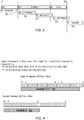
- FIG. 3 is a diagram depicting a number of addend shifts of varying lengths.
- the embodiment shown in FIG. 2 supports 64-bit mantissa values. Accordingly, the product would be 128 bits.
- the 66 bits to the left of the product are referred to as an increment region because when the addend and product are summed, the effect on the bits in that region is to add at most one unit.
- the 63 bits to the right of the product are referred to as the sticky region.
- the sticky region refers to the area which, if the addend is shifted such that any addend bits overlap the sticky region, those bits are logically OR-ed together to generate a sticky bit that may be used in rounding operations.
- the width of the sticky region may be defined as the mantissa width (Mw) minus one.
- the addend may need to be shifted such that the product and addend exponents are the same.
- the shift amounts may be confined to shifts where at least one bit of the shifted addend overlaps with the product, plus a few bits needed as guard banding for addends aligned to the left (more significant) than the product.
- guard bits (Gb) is chosen to be 2.
- a shift of zero would leave the addend with its bits in the range of 126:63, such as shown by addend 302 in FIG. 3 .
- a left shifted addend would be limited to a 67-bit shift, such that there are two guard bits between the LSB of the addend and the MSB of the product.
- an undershift condition would exist such that none of the addend bits align with the product bits as shown by undershift addend 301 in FIG. 3 . In practice it is considered simpler to shift in only one direction.
- a constant may be added to bias the shift amount so that an undershift is encoded as a shift of zero and the shifter always shifts to the right.
- addend 302 where addend exponent is equal to the exponent of the product, would result in a right shift of 67. All references to shift amounts hereinafter refer to this biased representation.
- shift addend 303 An addend shifted right by more than 2Mw+Gb but within a shift boundary is shown by shift addend 303, in which some of the bits of the shifted addend 303 are within the product and some are in the sticky range.
- the shift boundary may be defined as, for example, 3Mw + Gb -1. This shift boundary is 193 for the example datapath and is the maximum right shift since such a shift would allow the MSB of the addend to be aligned with the LSB of the product.
- the sticky range must include at least Mw-1 bits so that for this maximum right shift all the mantissa bits below the product LSB are included in the sticky. A right shift greater than the maximum is considered an overshift. Because the MSB of the addend is always 1, any overshift results in sticky being set.
- the overshift detection circuit may be built using an overshift threshold value selected anywhere between a the minimum and maximum overshift threshold.
- the minimum overshift threshold may be represented as the shifter width, which in this fused multiply implementation is Gb + 3Mw.
- the minimum and maximum overshift thresholds are 194 and 256, respectively.
- the overshift threshold is selected to be 256 or more as depicted by overshift addend 305, since as described further below, the logic to implement the overshift detection may have fewer logic levels and thus fewer gate delays.
- the sticky bit is forced to be set since there are no addend bits left in the sticky range to logically OR.
- FIG. 4 a diagram depicting an overshift detection logic simplification realization based upon the shifting shown in FIG. 3 is shown.
- the right shift amount i.e., shift value
- the exponents are represented as 18-bit unsigned numbers (e.g., ExpA[17:0]), however the shift value accounts for undershift values which are negative, thus the shifter includes an additional sign bit S[18].
- the detection logic compares the shift amount to an overshift threshold.
- two numbers X and Y are defined as shown.
- the X value would evaluate to be true if the sign bit was a logic value of zero, and any of bits [17:8] were a logic value of one.
- the maximum overshift threshold value may not be the optimum choice.
- an overshift threshold value may be selected that is between the minimum and a the maximum overshift thresholds and which has a largest number of a consecutive of bits that are zero beginning at the LSB of the value. More particularly, in the above example using 161 and 212 as the minimum and maximum overshift threshold values, 212 d corresponds to 11010100 b , while 192 d corresponds to 11000000 b .
- floating-point unit described above may be implemented in any type of processing unit capable of performing floating point functionality.
Claims (4)
- Gleitpunkteinheit:die dazu konfiguriert ist, eine Gleitpunktadditionsoperation zwischen einer ersten Gleitpunktzahl mit einem ersten Exponenten und einer ersten Mantisse und einer zweiten Gleitpunktzahl mit einem zweiten Exponenten und einer zweiten Mantisse durchzuführen, wobei die erste Gleitpunktzahl einem Produktwert entspricht, der sich aus einer Multiplikationsoperation zwischen zwei weiteren Gleitpunktzahlen ergibt, und das MSB der zweiten Mantisse eins ist;die dazu konfiguriert ist, einen Verschiebungswert zu berechnen, der einer Anzahl von Bitpositionen zum Verschieben der zweiten Mantisse entspricht, derart, dass der zweite Exponentenwert derselbe wie der erste Exponentenwert ist;die dazu konfiguriert ist, einen Zustand der übermäßigen Verschiebung zu erkennen, wobei der Verschiebungswert größer als oder gleich einem ausgewählten Schwellenwert für übermäßige Verschiebung ist;die dazu konfiguriert ist, in Reaktion auf den Zustand der übermäßigen Verschiebung eine Angabe für übermäßige Verschiebung bereitzustellen;die ferner dazu konfiguriert ist, zu bewirken, dass in Reaktion auf das Erkennen des Zustands der übermäßigen Verschiebung ein Sticky-Bit gesetzt wird;
dadurch gekennzeichnet, dassdie Anzahl von Schutzbits 2 beträgt und wobei die Mantissenbreite 24 beträgt und der Schwellenwert für übermäßige Verschiebung 96 beträgt oder die Mantissenbreite 53 beträgt und der Schwellenwert für übermäßige Verschiebung 192 beträgt oder die Mantissenbreite 64 beträgt und der Schwellenwert für übermäßige Verschiebung 256 beträgt. - Gleitpunkteinheit nach Anspruch 1, die ferner dazu konfiguriert ist, die zweite Mantisse um die Anzahl von Bitpositionen, die von dem Verschiebungswert angegeben wird, nach rechts zu verschieben.
- Gleitpunkteinheit nach Anspruch 1, wobei eine Anzahl von Bits rechts von einem niedrigstwertigen Bit (LSB) der ersten Mantisse der Sticky-Region entspricht, wobei die Sticky-Region eine Anzahl von Bits beinhaltet, die gleich eins minus eine Anzahl von Bits in einem Datenpfad der ersten Mantisse ist.
- Gleitpunkteinheit nach Anspruch 3, wobei in Reaktion darauf, dass die zweite Mantisse nach rechts verschoben wird, beliebige der LSBs der zweiten Mantisse, die rechts von dem LSB der ersten Mantisse liegen, mit einem logischen ODER miteinander verknüpft werden, um das Sticky-Bit zu erzeugen.
Applications Claiming Priority (2)
| Application Number | Priority Date | Filing Date | Title |
|---|---|---|---|
| US12/404,426 US8402075B2 (en) | 2009-03-16 | 2009-03-16 | Mechanism for fast detection of overshift in a floating point unit of a processing device |
| PCT/US2010/026908 WO2010107650A1 (en) | 2009-03-16 | 2010-03-11 | Mechanism for fast detection of overshift in a floating point unit |
Publications (2)
| Publication Number | Publication Date |
|---|---|
| EP2409219A1 EP2409219A1 (de) | 2012-01-25 |
| EP2409219B1 true EP2409219B1 (de) | 2017-04-19 |
Family
ID=42104634
Family Applications (1)
| Application Number | Title | Priority Date | Filing Date |
|---|---|---|---|
| EP10710952.2A Active EP2409219B1 (de) | 2009-03-16 | 2010-03-11 | Mechanismus zur schnellen detektion von overshift in einer floating-point-einheit |
Country Status (6)
| Country | Link |
|---|---|
| US (1) | US8402075B2 (de) |
| EP (1) | EP2409219B1 (de) |
| JP (1) | JP5719341B2 (de) |
| KR (1) | KR101528340B1 (de) |
| CN (1) | CN102349049B (de) |
| WO (1) | WO2010107650A1 (de) |
Families Citing this family (7)
| Publication number | Priority date | Publication date | Assignee | Title |
|---|---|---|---|---|
| US8694572B2 (en) * | 2010-07-06 | 2014-04-08 | Silminds, Llc, Egypt | Decimal floating-point fused multiply-add unit |
| US9354875B2 (en) * | 2012-12-27 | 2016-05-31 | Intel Corporation | Enhanced loop streaming detector to drive logic optimization |
| US20150193203A1 (en) * | 2014-01-07 | 2015-07-09 | Nvidia Corporation | Efficiency in a fused floating-point multiply-add unit |
| US10402168B2 (en) * | 2016-10-01 | 2019-09-03 | Intel Corporation | Low energy consumption mantissa multiplication for floating point multiply-add operations |
| US11200186B2 (en) | 2018-06-30 | 2021-12-14 | Intel Corporation | Apparatuses, methods, and systems for operations in a configurable spatial accelerator |
| US11907713B2 (en) | 2019-12-28 | 2024-02-20 | Intel Corporation | Apparatuses, methods, and systems for fused operations using sign modification in a processing element of a configurable spatial accelerator |
| JP7136478B2 (ja) | 2020-03-13 | 2022-09-13 | 株式会社東海理機 | ロータリバルブ |
Family Cites Families (21)
| Publication number | Priority date | Publication date | Assignee | Title |
|---|---|---|---|---|
| KR0139733B1 (ko) * | 1994-04-29 | 1998-07-01 | 구자홍 | 부동 소수점 덧셈/뺄셈 연산기의 반올림 방법 및 장치 |
| US5502401A (en) * | 1995-04-26 | 1996-03-26 | Texas Instruments Incorporated | Controllable width or gate |
| KR970016935A (ko) * | 1995-09-29 | 1997-04-28 | 김광호 | 부동소숫점 덧셈기에서 스티키비트 검출방법 |
| US5757686A (en) * | 1995-11-30 | 1998-05-26 | Hewlett-Packard Company | Method of decoupling the high order portion of the addend from the multiply result in an FMAC |
| JPH09204295A (ja) * | 1996-01-29 | 1997-08-05 | Kofu Nippon Denki Kk | スティッキービット検出回路 |
| US5771183A (en) * | 1996-06-28 | 1998-06-23 | Intel Corporation | Apparatus and method for computation of sticky bit in a multi-stage shifter used for floating point arithmetic |
| US5796644A (en) * | 1996-11-18 | 1998-08-18 | Samsung Electronics Company, Ltd. | Floating-point multiply-and-accumulate unit with classes for alignment and normalization |
| US6381624B1 (en) * | 1999-04-29 | 2002-04-30 | Hewlett-Packard Company | Faster multiply/accumulator |
| DE10050589B4 (de) * | 2000-02-18 | 2006-04-06 | Hewlett-Packard Development Co., L.P., Houston | Vorrichtung und Verfahren zur Verwendung beim Durchführen einer Gleitkomma-Multiplizier-Akkumulier-Operation |
| JP4086459B2 (ja) * | 2000-11-13 | 2008-05-14 | Necエレクトロニクス株式会社 | 固定小数点データ生成方法及び固定小数点データ生成回路 |
| US6754688B2 (en) * | 2001-02-14 | 2004-06-22 | Intel Corporation | Method and apparatus to calculate the difference of two numbers |
| US7080111B2 (en) * | 2001-06-04 | 2006-07-18 | Intel Corporation | Floating point multiply accumulator |
| US7003539B1 (en) * | 2001-08-08 | 2006-02-21 | Pasternak Solutions Llc | Efficiently determining a floor for a floating-point number |
| US6947962B2 (en) * | 2002-01-24 | 2005-09-20 | Intel Corporation | Overflow prediction algorithm and logic for high speed arithmetic units |
| CN1265281C (zh) * | 2002-07-29 | 2006-07-19 | 矽统科技股份有限公司 | 浮点数的对数运算方法和装置 |
| US7290023B2 (en) * | 2003-11-20 | 2007-10-30 | International Business Machines Corporation | High performance implementation of exponent adjustment in a floating point design |
| US8069200B2 (en) * | 2005-04-28 | 2011-11-29 | Qsigma, Inc. | Apparatus and method for implementing floating point additive and shift operations |
| JP4571903B2 (ja) * | 2005-12-02 | 2010-10-27 | 富士通株式会社 | 演算処理装置,情報処理装置,及び演算処理方法 |
| JP4413198B2 (ja) * | 2006-03-23 | 2010-02-10 | 富士通株式会社 | 浮動小数点データの総和演算処理方法及びコンピュータシステム |
| GB2447968B (en) * | 2007-03-30 | 2010-07-07 | Transitive Ltd | Improvements in and relating to floating point operations |
| US8214417B2 (en) * | 2008-08-14 | 2012-07-03 | Oracle America, Inc. | Subnormal number handling in floating point adder without detection of subnormal numbers before exponent subtraction |
-
2009
- 2009-03-16 US US12/404,426 patent/US8402075B2/en active Active
-
2010
- 2010-03-11 KR KR1020117023161A patent/KR101528340B1/ko active IP Right Grant
- 2010-03-11 EP EP10710952.2A patent/EP2409219B1/de active Active
- 2010-03-11 CN CN201080011918.6A patent/CN102349049B/zh active Active
- 2010-03-11 WO PCT/US2010/026908 patent/WO2010107650A1/en active Application Filing
- 2010-03-11 JP JP2012500839A patent/JP5719341B2/ja active Active
Non-Patent Citations (1)
| Title |
|---|
| None * |
Also Published As
| Publication number | Publication date |
|---|---|
| JP2012521047A (ja) | 2012-09-10 |
| CN102349049B (zh) | 2014-07-23 |
| US20100235416A1 (en) | 2010-09-16 |
| KR101528340B1 (ko) | 2015-06-11 |
| US8402075B2 (en) | 2013-03-19 |
| CN102349049A (zh) | 2012-02-08 |
| KR20120003878A (ko) | 2012-01-11 |
| JP5719341B2 (ja) | 2015-05-20 |
| WO2010107650A1 (en) | 2010-09-23 |
| EP2409219A1 (de) | 2012-01-25 |
Similar Documents
| Publication | Publication Date | Title |
|---|---|---|
| US6523050B1 (en) | Integer to floating point conversion using one's complement with subsequent correction to eliminate two's complement in critical path | |
| CN109643228B (zh) | 用于浮点乘加运算的低能耗尾数乘法 | |
| US7912887B2 (en) | Mode-based multiply-add recoding for denormal operands | |
| US7113969B1 (en) | Formatting denormal numbers for processing in a pipelined floating point unit | |
| US8386755B2 (en) | Non-atomic scheduling of micro-operations to perform round instruction | |
| US6490607B1 (en) | Shared FP and SIMD 3D multiplier | |
| EP2409219B1 (de) | Mechanismus zur schnellen detektion von overshift in einer floating-point-einheit | |
| US8577948B2 (en) | Split path multiply accumulate unit | |
| US6397239B2 (en) | Floating point addition pipeline including extreme value, comparison and accumulate functions | |
| US5917741A (en) | Method and apparatus for performing floating-point rounding operations for multiple precisions using incrementers | |
| US20060179266A1 (en) | System and method for generating effective address | |
| US20050223055A1 (en) | Method and apparatus to correct leading one prediction | |
| US6405232B1 (en) | Leading bit prediction with in-parallel correction | |
| US5764549A (en) | Fast floating point result alignment apparatus | |
| US6374345B1 (en) | Apparatus and method for handling tiny numbers using a super sticky bit in a microprocessor | |
| US6714957B1 (en) | System and method for efficient processing of denormal results as hardware exceptions | |
| US6965906B1 (en) | Converting negative floating point numbers to integer notation without two's complement hardware | |
| US6721772B1 (en) | Rounding denormalized numbers in a pipelined floating point unit without pipeline stalls | |
| EP0837390A1 (de) | Verbesserung an mikroprozessorbetriebenen integrierten Schaltungen oder damit zusammenhängend | |
| He et al. | Multiply-add fused float point unit with on-fly denormalized number processing |
Legal Events
| Date | Code | Title | Description |
|---|---|---|---|
| PUAI | Public reference made under article 153(3) epc to a published international application that has entered the european phase |
Free format text: ORIGINAL CODE: 0009012 |
|
| 17P | Request for examination filed |
Effective date: 20111004 |
|
| AK | Designated contracting states |
Kind code of ref document: A1 Designated state(s): AT BE BG CH CY CZ DE DK EE ES FI FR GB GR HR HU IE IS IT LI LT LU LV MC MK MT NL NO PL PT RO SE SI SK SM TR |
|
| DAX | Request for extension of the european patent (deleted) | ||
| 17Q | First examination report despatched |
Effective date: 20141217 |
|
| GRAP | Despatch of communication of intention to grant a patent |
Free format text: ORIGINAL CODE: EPIDOSNIGR1 |
|
| INTG | Intention to grant announced |
Effective date: 20161216 |
|
| GRAS | Grant fee paid |
Free format text: ORIGINAL CODE: EPIDOSNIGR3 |
|
| GRAA | (expected) grant |
Free format text: ORIGINAL CODE: 0009210 |
|
| AK | Designated contracting states |
Kind code of ref document: B1 Designated state(s): AT BE BG CH CY CZ DE DK EE ES FI FR GB GR HR HU IE IS IT LI LT LU LV MC MK MT NL NO PL PT RO SE SI SK SM TR |
|
| REG | Reference to a national code |
Ref country code: GB Ref legal event code: FG4D |
|
| REG | Reference to a national code |
Ref country code: CH Ref legal event code: EP |
|
| REG | Reference to a national code |
Ref country code: AT Ref legal event code: REF Ref document number: 886557 Country of ref document: AT Kind code of ref document: T Effective date: 20170515 |
|
| REG | Reference to a national code |
Ref country code: IE Ref legal event code: FG4D |
|
| REG | Reference to a national code |
Ref country code: DE Ref legal event code: R096 Ref document number: 602010041640 Country of ref document: DE |
|
| REG | Reference to a national code |
Ref country code: NL Ref legal event code: MP Effective date: 20170419 |
|
| REG | Reference to a national code |
Ref country code: LT Ref legal event code: MG4D |
|
| REG | Reference to a national code |
Ref country code: AT Ref legal event code: MK05 Ref document number: 886557 Country of ref document: AT Kind code of ref document: T Effective date: 20170419 |
|
| PG25 | Lapsed in a contracting state [announced via postgrant information from national office to epo] |
Ref country code: NL Free format text: LAPSE BECAUSE OF FAILURE TO SUBMIT A TRANSLATION OF THE DESCRIPTION OR TO PAY THE FEE WITHIN THE PRESCRIBED TIME-LIMIT Effective date: 20170419 |
|
| PG25 | Lapsed in a contracting state [announced via postgrant information from national office to epo] |
Ref country code: AT Free format text: LAPSE BECAUSE OF FAILURE TO SUBMIT A TRANSLATION OF THE DESCRIPTION OR TO PAY THE FEE WITHIN THE PRESCRIBED TIME-LIMIT Effective date: 20170419 Ref country code: FI Free format text: LAPSE BECAUSE OF FAILURE TO SUBMIT A TRANSLATION OF THE DESCRIPTION OR TO PAY THE FEE WITHIN THE PRESCRIBED TIME-LIMIT Effective date: 20170419 Ref country code: HR Free format text: LAPSE BECAUSE OF FAILURE TO SUBMIT A TRANSLATION OF THE DESCRIPTION OR TO PAY THE FEE WITHIN THE PRESCRIBED TIME-LIMIT Effective date: 20170419 Ref country code: NO Free format text: LAPSE BECAUSE OF FAILURE TO SUBMIT A TRANSLATION OF THE DESCRIPTION OR TO PAY THE FEE WITHIN THE PRESCRIBED TIME-LIMIT Effective date: 20170719 Ref country code: ES Free format text: LAPSE BECAUSE OF FAILURE TO SUBMIT A TRANSLATION OF THE DESCRIPTION OR TO PAY THE FEE WITHIN THE PRESCRIBED TIME-LIMIT Effective date: 20170419 Ref country code: LT Free format text: LAPSE BECAUSE OF FAILURE TO SUBMIT A TRANSLATION OF THE DESCRIPTION OR TO PAY THE FEE WITHIN THE PRESCRIBED TIME-LIMIT Effective date: 20170419 Ref country code: GR Free format text: LAPSE BECAUSE OF FAILURE TO SUBMIT A TRANSLATION OF THE DESCRIPTION OR TO PAY THE FEE WITHIN THE PRESCRIBED TIME-LIMIT Effective date: 20170720 |
|
| PG25 | Lapsed in a contracting state [announced via postgrant information from national office to epo] |
Ref country code: SE Free format text: LAPSE BECAUSE OF FAILURE TO SUBMIT A TRANSLATION OF THE DESCRIPTION OR TO PAY THE FEE WITHIN THE PRESCRIBED TIME-LIMIT Effective date: 20170419 Ref country code: PL Free format text: LAPSE BECAUSE OF FAILURE TO SUBMIT A TRANSLATION OF THE DESCRIPTION OR TO PAY THE FEE WITHIN THE PRESCRIBED TIME-LIMIT Effective date: 20170419 Ref country code: IS Free format text: LAPSE BECAUSE OF FAILURE TO SUBMIT A TRANSLATION OF THE DESCRIPTION OR TO PAY THE FEE WITHIN THE PRESCRIBED TIME-LIMIT Effective date: 20170819 Ref country code: LV Free format text: LAPSE BECAUSE OF FAILURE TO SUBMIT A TRANSLATION OF THE DESCRIPTION OR TO PAY THE FEE WITHIN THE PRESCRIBED TIME-LIMIT Effective date: 20170419 Ref country code: BG Free format text: LAPSE BECAUSE OF FAILURE TO SUBMIT A TRANSLATION OF THE DESCRIPTION OR TO PAY THE FEE WITHIN THE PRESCRIBED TIME-LIMIT Effective date: 20170719 |
|
| REG | Reference to a national code |
Ref country code: DE Ref legal event code: R097 Ref document number: 602010041640 Country of ref document: DE |
|
| PG25 | Lapsed in a contracting state [announced via postgrant information from national office to epo] |
Ref country code: EE Free format text: LAPSE BECAUSE OF FAILURE TO SUBMIT A TRANSLATION OF THE DESCRIPTION OR TO PAY THE FEE WITHIN THE PRESCRIBED TIME-LIMIT Effective date: 20170419 Ref country code: DK Free format text: LAPSE BECAUSE OF FAILURE TO SUBMIT A TRANSLATION OF THE DESCRIPTION OR TO PAY THE FEE WITHIN THE PRESCRIBED TIME-LIMIT Effective date: 20170419 Ref country code: CZ Free format text: LAPSE BECAUSE OF FAILURE TO SUBMIT A TRANSLATION OF THE DESCRIPTION OR TO PAY THE FEE WITHIN THE PRESCRIBED TIME-LIMIT Effective date: 20170419 Ref country code: SK Free format text: LAPSE BECAUSE OF FAILURE TO SUBMIT A TRANSLATION OF THE DESCRIPTION OR TO PAY THE FEE WITHIN THE PRESCRIBED TIME-LIMIT Effective date: 20170419 Ref country code: RO Free format text: LAPSE BECAUSE OF FAILURE TO SUBMIT A TRANSLATION OF THE DESCRIPTION OR TO PAY THE FEE WITHIN THE PRESCRIBED TIME-LIMIT Effective date: 20170419 |
|
| PLBE | No opposition filed within time limit |
Free format text: ORIGINAL CODE: 0009261 |
|
| STAA | Information on the status of an ep patent application or granted ep patent |
Free format text: STATUS: NO OPPOSITION FILED WITHIN TIME LIMIT |
|
| PG25 | Lapsed in a contracting state [announced via postgrant information from national office to epo] |
Ref country code: IT Free format text: LAPSE BECAUSE OF FAILURE TO SUBMIT A TRANSLATION OF THE DESCRIPTION OR TO PAY THE FEE WITHIN THE PRESCRIBED TIME-LIMIT Effective date: 20170419 Ref country code: SM Free format text: LAPSE BECAUSE OF FAILURE TO SUBMIT A TRANSLATION OF THE DESCRIPTION OR TO PAY THE FEE WITHIN THE PRESCRIBED TIME-LIMIT Effective date: 20170419 |
|
| 26N | No opposition filed |
Effective date: 20180122 |
|
| PG25 | Lapsed in a contracting state [announced via postgrant information from national office to epo] |
Ref country code: SI Free format text: LAPSE BECAUSE OF FAILURE TO SUBMIT A TRANSLATION OF THE DESCRIPTION OR TO PAY THE FEE WITHIN THE PRESCRIBED TIME-LIMIT Effective date: 20170419 |
|
| REG | Reference to a national code |
Ref country code: CH Ref legal event code: PL |
|
| PG25 | Lapsed in a contracting state [announced via postgrant information from national office to epo] |
Ref country code: MC Free format text: LAPSE BECAUSE OF FAILURE TO SUBMIT A TRANSLATION OF THE DESCRIPTION OR TO PAY THE FEE WITHIN THE PRESCRIBED TIME-LIMIT Effective date: 20170419 |
|
| REG | Reference to a national code |
Ref country code: BE Ref legal event code: MM Effective date: 20180331 |
|
| REG | Reference to a national code |
Ref country code: IE Ref legal event code: MM4A |
|
| PG25 | Lapsed in a contracting state [announced via postgrant information from national office to epo] |
Ref country code: LU Free format text: LAPSE BECAUSE OF NON-PAYMENT OF DUE FEES Effective date: 20180311 |
|
| PG25 | Lapsed in a contracting state [announced via postgrant information from national office to epo] |
Ref country code: IE Free format text: LAPSE BECAUSE OF NON-PAYMENT OF DUE FEES Effective date: 20180311 |
|
| PG25 | Lapsed in a contracting state [announced via postgrant information from national office to epo] |
Ref country code: BE Free format text: LAPSE BECAUSE OF NON-PAYMENT OF DUE FEES Effective date: 20180331 Ref country code: LI Free format text: LAPSE BECAUSE OF NON-PAYMENT OF DUE FEES Effective date: 20180331 Ref country code: CH Free format text: LAPSE BECAUSE OF NON-PAYMENT OF DUE FEES Effective date: 20180331 |
|
| PG25 | Lapsed in a contracting state [announced via postgrant information from national office to epo] |
Ref country code: FR Free format text: LAPSE BECAUSE OF NON-PAYMENT OF DUE FEES Effective date: 20180331 |
|
| PG25 | Lapsed in a contracting state [announced via postgrant information from national office to epo] |
Ref country code: MT Free format text: LAPSE BECAUSE OF NON-PAYMENT OF DUE FEES Effective date: 20180311 |
|
| PG25 | Lapsed in a contracting state [announced via postgrant information from national office to epo] |
Ref country code: TR Free format text: LAPSE BECAUSE OF FAILURE TO SUBMIT A TRANSLATION OF THE DESCRIPTION OR TO PAY THE FEE WITHIN THE PRESCRIBED TIME-LIMIT Effective date: 20170419 |
|
| PG25 | Lapsed in a contracting state [announced via postgrant information from national office to epo] |
Ref country code: HU Free format text: LAPSE BECAUSE OF FAILURE TO SUBMIT A TRANSLATION OF THE DESCRIPTION OR TO PAY THE FEE WITHIN THE PRESCRIBED TIME-LIMIT; INVALID AB INITIO Effective date: 20100311 Ref country code: PT Free format text: LAPSE BECAUSE OF FAILURE TO SUBMIT A TRANSLATION OF THE DESCRIPTION OR TO PAY THE FEE WITHIN THE PRESCRIBED TIME-LIMIT Effective date: 20170419 |
|
| PG25 | Lapsed in a contracting state [announced via postgrant information from national office to epo] |
Ref country code: MK Free format text: LAPSE BECAUSE OF NON-PAYMENT OF DUE FEES Effective date: 20170419 Ref country code: CY Free format text: LAPSE BECAUSE OF FAILURE TO SUBMIT A TRANSLATION OF THE DESCRIPTION OR TO PAY THE FEE WITHIN THE PRESCRIBED TIME-LIMIT Effective date: 20170419 |
|
| P01 | Opt-out of the competence of the unified patent court (upc) registered |
Effective date: 20230530 |
|
| PGFP | Annual fee paid to national office [announced via postgrant information from national office to epo] |
Ref country code: DE Payment date: 20240325 Year of fee payment: 15 Ref country code: GB Payment date: 20240318 Year of fee payment: 15 |