EP2405505A1 - Organic semiconductor material and organic thin film transistor - Google Patents
Organic semiconductor material and organic thin film transistor Download PDFInfo
- Publication number
- EP2405505A1 EP2405505A1 EP10748817A EP10748817A EP2405505A1 EP 2405505 A1 EP2405505 A1 EP 2405505A1 EP 10748817 A EP10748817 A EP 10748817A EP 10748817 A EP10748817 A EP 10748817A EP 2405505 A1 EP2405505 A1 EP 2405505A1
- Authority
- EP
- European Patent Office
- Prior art keywords
- organic semiconductor
- unsubstituted
- residue
- semiconductor material
- substituted
- Prior art date
- Legal status (The legal status is an assumption and is not a legal conclusion. Google has not performed a legal analysis and makes no representation as to the accuracy of the status listed.)
- Granted
Links
- 0 *C1C=*C(C(C/C2=C\CC(C=C([C@@]3CC=C(*)CC3)C#N)/C=C/C=C2)C#N)=CC1 Chemical compound *C1C=*C(C(C/C2=C\CC(C=C([C@@]3CC=C(*)CC3)C#N)/C=C/C=C2)C#N)=CC1 0.000 description 3
Images



Classifications
-
- C—CHEMISTRY; METALLURGY
- C07—ORGANIC CHEMISTRY
- C07D—HETEROCYCLIC COMPOUNDS
- C07D495/00—Heterocyclic compounds containing in the condensed system at least one hetero ring having sulfur atoms as the only ring hetero atoms
- C07D495/02—Heterocyclic compounds containing in the condensed system at least one hetero ring having sulfur atoms as the only ring hetero atoms in which the condensed system contains two hetero rings
- C07D495/04—Ortho-condensed systems
-
- C—CHEMISTRY; METALLURGY
- C07—ORGANIC CHEMISTRY
- C07C—ACYCLIC OR CARBOCYCLIC COMPOUNDS
- C07C255/00—Carboxylic acid nitriles
- C07C255/01—Carboxylic acid nitriles having cyano groups bound to acyclic carbon atoms
- C07C255/32—Carboxylic acid nitriles having cyano groups bound to acyclic carbon atoms having cyano groups bound to acyclic carbon atoms of a carbon skeleton containing at least one six-membered aromatic ring
- C07C255/34—Carboxylic acid nitriles having cyano groups bound to acyclic carbon atoms having cyano groups bound to acyclic carbon atoms of a carbon skeleton containing at least one six-membered aromatic ring with cyano groups linked to the six-membered aromatic ring, or to the condensed ring system containing that ring, by unsaturated carbon chains
-
- C—CHEMISTRY; METALLURGY
- C07—ORGANIC CHEMISTRY
- C07C—ACYCLIC OR CARBOCYCLIC COMPOUNDS
- C07C255/00—Carboxylic acid nitriles
- C07C255/01—Carboxylic acid nitriles having cyano groups bound to acyclic carbon atoms
- C07C255/32—Carboxylic acid nitriles having cyano groups bound to acyclic carbon atoms having cyano groups bound to acyclic carbon atoms of a carbon skeleton containing at least one six-membered aromatic ring
- C07C255/35—Carboxylic acid nitriles having cyano groups bound to acyclic carbon atoms having cyano groups bound to acyclic carbon atoms of a carbon skeleton containing at least one six-membered aromatic ring the carbon skeleton being further substituted by halogen atoms, or by nitro or nitroso groups
-
- C—CHEMISTRY; METALLURGY
- C07—ORGANIC CHEMISTRY
- C07C—ACYCLIC OR CARBOCYCLIC COMPOUNDS
- C07C255/00—Carboxylic acid nitriles
- C07C255/01—Carboxylic acid nitriles having cyano groups bound to acyclic carbon atoms
- C07C255/32—Carboxylic acid nitriles having cyano groups bound to acyclic carbon atoms having cyano groups bound to acyclic carbon atoms of a carbon skeleton containing at least one six-membered aromatic ring
- C07C255/37—Carboxylic acid nitriles having cyano groups bound to acyclic carbon atoms having cyano groups bound to acyclic carbon atoms of a carbon skeleton containing at least one six-membered aromatic ring the carbon skeleton being further substituted by etherified hydroxy groups
-
- C—CHEMISTRY; METALLURGY
- C07—ORGANIC CHEMISTRY
- C07C—ACYCLIC OR CARBOCYCLIC COMPOUNDS
- C07C255/00—Carboxylic acid nitriles
- C07C255/01—Carboxylic acid nitriles having cyano groups bound to acyclic carbon atoms
- C07C255/32—Carboxylic acid nitriles having cyano groups bound to acyclic carbon atoms having cyano groups bound to acyclic carbon atoms of a carbon skeleton containing at least one six-membered aromatic ring
- C07C255/40—Carboxylic acid nitriles having cyano groups bound to acyclic carbon atoms having cyano groups bound to acyclic carbon atoms of a carbon skeleton containing at least one six-membered aromatic ring the carbon skeleton being further substituted by doubly-bound oxygen atoms
-
- H—ELECTRICITY
- H10—SEMICONDUCTOR DEVICES; ELECTRIC SOLID-STATE DEVICES NOT OTHERWISE PROVIDED FOR
- H10K—ORGANIC ELECTRIC SOLID-STATE DEVICES
- H10K85/00—Organic materials used in the body or electrodes of devices covered by this subclass
- H10K85/60—Organic compounds having low molecular weight
- H10K85/649—Aromatic compounds comprising a hetero atom
- H10K85/657—Polycyclic condensed heteroaromatic hydrocarbons
- H10K85/6572—Polycyclic condensed heteroaromatic hydrocarbons comprising only nitrogen in the heteroaromatic polycondensed ring system, e.g. phenanthroline or carbazole
-
- H—ELECTRICITY
- H10—SEMICONDUCTOR DEVICES; ELECTRIC SOLID-STATE DEVICES NOT OTHERWISE PROVIDED FOR
- H10K—ORGANIC ELECTRIC SOLID-STATE DEVICES
- H10K85/00—Organic materials used in the body or electrodes of devices covered by this subclass
- H10K85/60—Organic compounds having low molecular weight
- H10K85/649—Aromatic compounds comprising a hetero atom
- H10K85/657—Polycyclic condensed heteroaromatic hydrocarbons
- H10K85/6574—Polycyclic condensed heteroaromatic hydrocarbons comprising only oxygen in the heteroaromatic polycondensed ring system, e.g. cumarine dyes
-
- H—ELECTRICITY
- H10—SEMICONDUCTOR DEVICES; ELECTRIC SOLID-STATE DEVICES NOT OTHERWISE PROVIDED FOR
- H10K—ORGANIC ELECTRIC SOLID-STATE DEVICES
- H10K85/00—Organic materials used in the body or electrodes of devices covered by this subclass
- H10K85/60—Organic compounds having low molecular weight
- H10K85/649—Aromatic compounds comprising a hetero atom
- H10K85/657—Polycyclic condensed heteroaromatic hydrocarbons
- H10K85/6576—Polycyclic condensed heteroaromatic hydrocarbons comprising only sulfur in the heteroaromatic polycondensed ring system, e.g. benzothiophene
-
- H—ELECTRICITY
- H10—SEMICONDUCTOR DEVICES; ELECTRIC SOLID-STATE DEVICES NOT OTHERWISE PROVIDED FOR
- H10K—ORGANIC ELECTRIC SOLID-STATE DEVICES
- H10K10/00—Organic devices specially adapted for rectifying, amplifying, oscillating or switching; Organic capacitors or resistors having potential barriers
- H10K10/40—Organic transistors
- H10K10/46—Field-effect transistors, e.g. organic thin-film transistors [OTFT]
- H10K10/462—Insulated gate field-effect transistors [IGFETs]
- H10K10/466—Lateral bottom-gate IGFETs comprising only a single gate
-
- H—ELECTRICITY
- H10—SEMICONDUCTOR DEVICES; ELECTRIC SOLID-STATE DEVICES NOT OTHERWISE PROVIDED FOR
- H10K—ORGANIC ELECTRIC SOLID-STATE DEVICES
- H10K10/00—Organic devices specially adapted for rectifying, amplifying, oscillating or switching; Organic capacitors or resistors having potential barriers
- H10K10/40—Organic transistors
- H10K10/46—Field-effect transistors, e.g. organic thin-film transistors [OTFT]
- H10K10/462—Insulated gate field-effect transistors [IGFETs]
- H10K10/481—Insulated gate field-effect transistors [IGFETs] characterised by the gate conductors
Definitions
- the present invention relates to organic semiconductor materials and to organic thin-film transistors having a layer of the organic semiconductor material.
- organic electronic devices using carrier-conductive organic compounds have been developed actively. Such organic compounds have been applied to light emitting materials, charge injection materials and charge conductive materials for organic EL devices, and organic laser oscillators (for example, see Patent Documents 1 and 2). The application of those organic compounds to organic thin-film transistor has been expected. Thin film transistors have been widely applied to switching elements for display devices such as liquid crystal displays. Although amorphous or polycrystalline silicon has been employed to the thin-film transistor, the transistor using the organic semiconductor material has been proposed in terms of its low production cost and productivity. Several organic compounds used as the organic semiconductor material have been reported.
- Patent Document 3 discloses conjugated or non-conjugated oligomers and polymers having a stilbene structure as novel organic compounds for the organic semiconductor materials with high carrier mobility.
- Patent Document 4 discloses that the response rate (carrier mobility) of the organic thin-film transistor may be enhanced by using a certain organic compound having styryl group for the organic semiconductor layer.
- the organic semiconductor material used for the organic semiconductor layer of light emitting material, charge injection materials and charge conductive materials of transistors and organic EL devices or the organic laser oscillators and the like it is essential for the organic semiconductor material used for the organic semiconductor layer of light emitting material, charge injection materials and charge conductive materials of transistors and organic EL devices or the organic laser oscillators and the like to have excellent properties in all aspects such as resistance against oxygen and water, good workability as well as excellent physical, chemical and electronic connectivity with various electrode materials in addition to high carrier conductivity as the organic semiconductor material.
- the carrier mobility of the compounds as disclosed in Patent Document 3 are insufficient for the organic semiconductor layer.
- the compounds as disclosed in Patent Document 4 exhibit n-type semiconductor properties and have high carrier (electron) mobility. However, resistance against oxygen and water of those compounds is insufficient.
- a highly reactive metal such as calcium must be used as a cathode because of its shallow LUMO levels, electron injection levels of those compounds.
- formation of the films of conventional organic semiconductor materials using a simple process such as a coating process is difficult because of their poor solubility in organic solvents and poor affinity to various substrate materials.
- the object of present invention is to provide an organic semiconductor material having excellent carrier (electron) mobility, stability, and film-forming ability using a simple production process, as well as an organic thin-film transistor in which the material is used in an organic semiconductor layer.
- the present invention relates to an organic semiconductor material as follows:
- the organic semiconductor material of the present invention has high carrier mobility, excellent physical, chemical and electronic connectivity with various electrode materials, and high stability to air and moisture. Accordingly, the organic semiconductor material of the present invention has excellent properties for practical use in all aspects as an organic semiconductor layer for an organic thin-film-transistor. Thus, it is preferably applicable to the organic semiconductor layer for the organic thin-film transistor. In addition, the organic semiconductor material of the present invention has an advantage of film-forming ability using a simple coating process because of its high solubility in conventional organic solvents.
- the first characteristic of the organic semiconductor material of the present invention is the structure represented by the general formula (1) shown below.
- the compound represented by the general formula (1) may be referred to as "the compound of the present invention”.
- L represents a bivalent linker group having the structure consisting of one group or any combination of two or more groups selected from unsubstituted or substituted vinylene group, acetylene group, unsubstituted or substituted aromatic hydrocarbon residue, unsubstituted or substituted fused aromatic hydrocarbon residue, unsubstituted or substituted heteroaromatic residue, unsubstituted or substituted fused heteroaromatic residue.
- the aforementioned aromatic hydrocarbon residue includes benzene residue.
- the fused aromatic hydrocarbon residue includes naphthalene residue, phenanthrene residue, anthracene residue, perylene residue, pyrene residue, chrysene residue, pentacene residue, phenazine residue, tetracene residue, triphenylene residue, picene residue and the like.
- the heteroaromatic residue includes thiophene residue, furan residue, pyrrole residue, pyrazole residue, imidazole residue, triazole residue, oxazole residue, thiazole residue, thiadiazole residue, pyridine residue, pyrimidine residue, triazine residue, pyradine residue and the like.
- the fused heteroaromatic residue includes fluorene residue, indole residue, carbazole residue, benzothiophene residue, benzofuran residue, thienothiophene residue, thiazolothiazole residue, dibenzothiophene residue, dibenzofuran residue, dithienothiophene residue, benzoimidazole residue, benzooxazole residue, purine residue, benzothiophenebenzothiophene residue, dibenzobenzodifuran residue, acrydine residue, quinoline residue and the like.
- the preferable example of the L includes the group having the structure consisting of one group or any combination of two or more groups selected from unsubstituted or substituted vinylene group, unsubstituted or substituted benzene residue, unsubstituted or substituted naphthalene residue, unsubstituted or substituted anthracene residue, unsubstituted or substituted perylene residue, unsubstituted or substituted pyrene residue, unsubstituted or substituted thiophene residue, unsubstituted or substituted furan residue, unsubstituted or substituted pyrrole residue, unsubstituted or substituted thiazole residue, unsubstituted or substituted benzothiophene residue, unsubstituted or substituted benzofuran residue, unsubstituted or substituted thienothiophene residue.
- the main molecular skeleton, L has the structure preferably consisting of four or less groups selected from the aforementioned groups, more preferably consisting of two or less groups selected from the aforementioned groups.
- the more preferable example of the L includes unsubstituted benzene residue represented by formula (2) shown below, unsubstituted thiophene residue represented by formula (3) shown below, unsubstituted thienothiophene residue represented by formula (4) shown below, unsubstituted furan residue represented by formula (5) shown below, and unsubstituted pyrrole residue represented by formula (6) shown below, in which unsubstituted benzene residue, unsubstituted thiophene residue and unsubstituted thienothiophene residue are particularly preferred.
- R 1 represents carbonyl group, cyano group or C 1 -C 12 fluorinated alkyl group.
- fluorinated alkyl group is particularly preferred.
- R 1 is fluorinated alkyl group, orderliness is brought to the compound because of not only electron-withdrawing property of fluorine atom but also interaction between the fluorinated alkyl groups. As a result, the compound of the present invention tends to become more crystalline.
- the carbon number of the fluorinated alkyl group of the compound of the present invention is 1 to 12, preferably 1 to 6, particularly preferably 1 to 3.
- R 2 represents electron withdrawing halogen atom, cyano group or acetyl group.
- cyano group is particularly preferred in the compound of the present invention represented by the general formula (1) since it contributes to crystallinity of the compound to enhance the intermolecular interaction without undue steric hindrance.
- Compounds (A1) - (A4) may be exemplified as examples in which L consists of aromatic hydrocarbon residue.
- Compounds (B1) - (B6) may be exemplified as examples in which L consists of fused aromatic hydrocarbon residue.
- Compounds (D1) - (D6) may be exemplified as examples in which L consists of aromatic fused heterocyclic hydrocarbon residue.
- Compounds (F1) - (F4) may be exemplified as examples in which R 1 is halogenated alkyl group.
- Compounds (G1) - (G5) may be exemplified as examples in which L has the structure consisting of the combination of at least two of aromatic ring, heterocycle, and vinylene group.
- Compounds (H1) - (H7) may be exemplified as examples in which L particularly has the structure consisting of the combination of fused aromatic ring and fused heterocycle among the examples in which L consists of fused heteroaromatic group.
- the compound having crystallinity is particularly preferred.
- the compound of the present invention has crystallinity, a short intermolecular distance facilitates electron transfer. Also, it has the advantage of stable electronic property because of a constant intermolecular distance.
- the terms "crystalline” and “have crystallinity” mean that second or higher order reflection may be substantially observed in X-ray diffraction (XRD) measurement.
- the compound of the present invention may be preferably applied to the organic semiconductor layer in the form of thin-film having the thickness of about 1 ⁇ m or less. Accordingly, it is desirable that the compound of the present invention has crystallinity not only in bulk form but also in the form of a thin-film organic semiconductor layer.
- the compound of the present invention preferably has a symmetry and it is particularly preferable that it has a point symmetry center.
- the compounds with a plane symmetry include the compounds (C1), (C3), (D2) and (H5).
- the compounds with a point symmetry include the compounds (A1)-(A4), (B1)-(B6), (C2), (C4)-(C7), (D1), (D3)-(D6), (E1)-(E4), (E6), (E7), (F1)-(F4), (G1)-(G4), (H1)-(H7), and (I1)-(I3)
- the aforementioned compounds of the present invention have a high carrier mobility, which is 0.01[cm 2 /V ⁇ sec] or more even without removing oxygen and moisture. Also, the compound of the present invention is highly stable against air (oxygen) and moisture and hard to be oxidized.
- the compound of the present invention is soluble in conventional organic solvents as described below. Accordingly, the thin film of the compound of the present invention may be formed by means of coating method such as cast coating, spin coating, screen printing, and inkjet printing using the solution prepared by dissolving the compound of the present invention in appropriate solvent and optionally adding additive.
- the solvent is not particularly limited so far as it may dissolve the compound of the present invention to an appropriate concentration.
- the example of the solvent includes haloalkane solvents such as chloroform and 1,2-dichloroethane; aromatic solvents such as toluene, o-dichlorobenzene, nitrobenzene and m-cresol; N-methylpyrrolidone and carbon disulfide.
- One compound or any combination of two or more compounds selected from the compounds of the present invention may be employed. Also, more than one mixed thin films or laminated films may be formed by using organic semiconductor material known in the art such as pentacene, thiophene oligomer and fullerene together with the compound of the present invention.
- the compound of the present invention may be synthesized by means of any methods known in the art of organic synthesis. Particular methods include bromination, cyanizaiton and aldehyde formation. Knoevenagel condensation reaction is preferably carried out as the final step of the synthesis since the yield of 70% or more may be achieved.
- the compounds of the present invention are soluble in conventional organic solvents as well as they have stability against air and moisture. Accordingly, the organic semiconductor layer for organic thin-film transistors having superior properties and high reliability may be formed with coating process by using simple device, although it may also be formed on substrate by vacuum sputtering process.
- Fig. 1 shows a schematic cross sectional view of one of the organic thin-film transistors having the organic semiconductor layer consisting of the organic semiconductor material of the present invention.
- the organic thin-film transistor 10 (hereinafter, it may be abbreviated to "transistor 10"), has the structure in which a gate electrode 2, a gate insulator layer 3, and an organic semiconductor layer 4 are laminated on a substrate 1 in that order, and a pair of a source electrode 5 and a drain electrode 6 are formed on the organic semiconductor layer 4.
- the structure shown here is one embodiment of the organic thin-film transistor using the organic semiconductor material of the present invention.
- the organic semiconductor material of the present invention may be applicable not only to the organic thin-film transistor as shown in Fig. 1 , but also to any organic thin-film transistors including the one as shown in Fig. 2 .
- the substrate 1 is for ensuring the self-supporting property of the transistor 10.
- the material used for the substrate 1 is not particularly limited and various substrates such as the one made of glass, resins and semiconductor materials such as Si may be preferably employed.
- the Si substrate is preferably employed from the viewpoint of workability and the mechanical strength of the substrate.
- highly flexible resins such as polyethylene naphthalate (PEN) may be preferably employed as the substrate 1.
- the substrate 1 and the gate electrode 2 are formed by using different materials, however, from the viewpoint of the self-supporting property of the transistor 10, the gate electrode 2 having the thickness sufficient to be a self-supporting film (self-supporting layer) may be employed so that it may act as the substrate 1 as well.
- the gate electrode 2 is used for controlling the source-drain current.
- the material used for the gate electrode 2 is not particularly limited as long as it is conductive.
- metals such as chromium (Cr), tantalum (Ta), titanium (Ti), copper (Cu), aluminum (Al), molybdenum (Mo), tungsten (W), nickel (Ni), gold (Au), palladium (Pd), platinum (Pt), silver (Ag), tin (Sn), lithium (Li) and calcium (Ca); oxides of these metals; indium tin oxide (ITO) and zinc oxide (ZnO); conductive polymers known in the art such as conductive polyaniline, conductive polypyrrole and conductive polythiazyl may preferably be used as the material for the gate electrode 2.
- the thickness of the gate electrode 2 is not particularly limited, which is typically from 10 nm to 150 mm. On the other hand, if the gate electrode 2 also serves as the substrate, the thickness of the gate electrode 2 is preferably from 10 ⁇ m to 0.5 mm to ensure sufficient self-supporting property.
- the gate insulator layer 3 is formed between the gate electrode 2 and the organic semiconductor layer 4.
- the material used for the gate insulator layer 3 is not limited so far as it has the aforementioned function.
- the gate insulator layer 3 may be the insulator layer consisting of at least one of metal oxide film such as silicon oxide (SiO 2 ) aluminum oxide (Al 2 O 3 ) and tantulum oxide (Ta 2 O 5 ); organic compound such as polyvinylphenol, polyimide, polyvinyl alcohol, polyethylene, polyethyleneterephthalate, polyvinylidene fluoride, polymethylmethacrylate, polycarbonate, polyethylene fluoride, polystyrene, polyxylylene, cellulose, pullulan and CytopTM.
- metal oxide film such as silicon oxide (SiO 2 ) aluminum oxide (Al 2 O 3 ) and tantulum oxide (Ta 2 O 5 )
- organic compound such as polyvinylphenol, polyimide, polyvinyl alcohol, polyethylene, polyethylene
- Si substrate which is preferred when the gate electrode 2 also serves as the substrate is used as the gate electrode 2
- SiO 2 formed by oxidizing its surface may be used as the gate insulator layer 3.
- the thickness of the gate insulator layer 3 is not particularly limited so far as electronic insulation between the gate electrode 2 and the source electrode 5, which is typically from 100 to 1000 nm.
- the organic semiconductor layer 4 consists of the organic semiconductor material of the present invention.
- any film formation (deposition) processes known in the art may employed without limitation.
- the example of the process includes the process in which the organic semiconductor layer 4 is formed by coating the solution prepared by dissolving the compound of the present invention in appropriate solvent by means of the coating method known in the art such as cast coating, spin coating, screen printing, inkjet printing and ablation (hereinafter, abbreviated to "coating process”); and gas phase film formation process such as vacuum deposition.
- the solvent is not particularly limited so far as it may dissolve the compound of the present invention to an appropriate concentration.
- the example of the solvent includes haloalkyl solvents such as chloroform and 1,2-dichloroethane; aromatic solvents such as toluene, o-dichlorobenzene, nitrobenzene and m-cresol; N-methylpyrrolidone and carbon disulfide.
- Most of the compounds of the present invention are soluble in general organic solvents.
- CF 3 CN-DSB may be favorably coated by dissolving in chloroform or toluene.
- the cost required for the gas-phase deposition process may be higher than that for the coating process, the compound of the present invention contained in the organic semiconductor layer 4 tends to be more crystalline. Accordingly, the transistor of higher performance may be fabricated.
- the vacuum deposition process is particularly preferable from the viewpoint of the film quality.
- the thickness of the organic semiconductor layer 4 is not particularly limited. However, the performance of the transistor obtained strongly depend on the thickness of the active layer consisting of the organic semiconductor.
- the thickness of the organic semiconductor layer 4 depends on the organic semiconductor, which is generally 1 ⁇ m or less, particularly preferably from 10 to 300 nm.
- the source electrode 5 and the drain electrode 6 are a pair of electrodes formed on the organic semiconductor layer 4. Current may be supplied from the source electrode 5 to the drain electrode 6 via the organic semiconductor layer 4.
- the material used for the source electrode 5 and the drain electrode 6 is not particularly limited so far as it is conductive, which includes the materials similar to those used for the aforementioned gate electrode 2. Among those materials, the material having small resistance on the surface in contact with the organic semiconductor layer 4 is preferred.
- the example of such material includes Cu, Ag, Pt, Au and Au, which is chemically stable and catalytically inert is particularly preferred.
- the example of the process for forming such electrodes includes the process in which the electrode formation is carried out by vacuum deposition or sputtering of the aforementioned material through a shadow mask located on the organic semiconductor layer; the process in which the thin-film of the aforementioned material formed by vacuum deposition or sputtering is shaped by photolithographic method or lift-off method known in the art; thermal transfer of metal foil; and etching the thin-film of the aforementioned material using resist formed by inkjet printing and the like.
- the examples of the process also include the process in which the electrode formation is carried out by coating a solution or a dispersion of conductive polymer, or a dispersion of conductive microparticulate by direct inkjet printing on a certain pattern; the process in which electrode formation is carried out by lithography and laser ablation of the coated film of the aforementioned material; and the like.
- the reagents used are as follows:
- organic semiconductor material 1 (2Z,2'Z)-3,3'-(1,4-phenylene)bis(2-(4-trifluoromethyl)phenylacrylonitrile) (abbrev.: CF 3 CN-DSB, compound (Al), yellow crystal). Yield: 775 mg (80%).
- a silicon wafer with 300 nm of thermally oxidized silicon dioxide film (SUMCO CORPORATION, 1 ⁇ 1 cm (area: 1cm 2 ), thickness: 525 ⁇ m) was used as a gate electrode and a gate insulator layer.
- a organic semiconductor layer was formed by vacuum deposition (deposition conditions were as follows. pressure: ca. 4.0 ⁇ 10 -6 torr,-deposition rate: 0.5 nm/min, substrate temperature: room temperature ( ca. 25°C)) of the organic semiconductor material 1 under the condition which afforded the film thickness of ca. 50 nm on top of the silicon dioxide film.
- a source electrode and a drain electrode of Au having the thickness of ca.
- Channel length (L) and channel width (W) of the source and the drain electrodes are 20 ⁇ m and 2 mm, respectively.
- An organic thin-film transistor 2 according to Example 2 having the structure as shown in Fig. 1 was obtained according to the procedure similar to that of Example 1 except that the organic semiconductor material 2 was used instead of the organic semiconductor material 1.
- An organic thin film transistor 3 according to Example 3 having the structure as shown in Fig. 1 was obtained according to the procedure similar to that of Example 1 except that the organic semiconductor material 3 was used instead of the organic semiconductor material 1.
- An organic thin film transistor 4 according to Example 4 having the structure as shown in Fig. 1 was obtained according to the procedure similar to that of Example 1 except that the organic semiconductor material 4 was used instead of the organic semiconductor material 1.
- An organic thin film transistor 5 according to Example 5 having the structure as shown in Fig. 1 was obtained according to the procedure similar to that of Example 1 except that the organic semiconductor material 5 was used instead of the organic semiconductor material 1.
- An organic thin film transistor 6 according to Example 6 having the structure as shown in Fig. 1 was obtained according to the procedure similar to that of Example 1 except that the organic semiconductor material 6 was used instead of the organic semiconductor material 1.
- An organic thin film transistor 7 according to Example 7 having the structure as shown in Fig. 1 was obtained according to the procedure similar to that of Example 1 except that the organic semiconductor material 7 was used instead of the organic semiconductor material 1.
- An organic semiconductor material 8 (2Z,2'Z)-3,3'-(1,4-phenylene)bis(2-(4-methyl)phenylacrylonitrile) (abbrev.: CH 3 CN-DSB) was synthesized according to the procedure similar to that of Example 1 except that the 4-methylphenylacetonitrile was used instead of 4-trifluoromethylphenylacetonitrile.
- An organic thin film transistor 8 according to Comparative example 1 having the structure as shown in Fig. 1 was obtained according to the procedure similar to that of Example 1 except that the organic semiconductor material 8 was used instead of the organic semiconductor material 1.
- An organic semiconductor material 9 (2Z,2'Z)-3,3'-(1,4-phenylene)bis(2-(4-fluoro)phenylacrylonitrile) (abbrev.: FCN-DSB) was synthesized according to the procedure similar to that of Example 1 except that the 4-fluorophenylacetonitrile was used instead of 4-trifluoromethylphenylacetonitrile.
- An organic thin film transistor 9 according to Comparative example 2 having the structure as shown in Fig. 1 was obtained according to the procedure similar to that of Example 1 except that the organic semiconductor material 9 was used instead of the organic semiconductor material 1.
- the organic semiconductor material 1 (2Z,2'Z)-3,3'-(1,4-phenylene)bis(2-(4-trifluoromethyl)phenylacrylonitrile) (abbrev.: CF 3 CN-DSB, compound (A1)) was synthesized according to the procedure similar to that of Examples 1.
- a PEN film (thickness: 100 ⁇ m) was used instead of a silicon wafer with thermal oxidized film, on which a gate electrode was formed by vacuum deposition of Au (40 nm)/Ti (5 nm).
- An organic thin film transistor 10 according to Example 8 having the structure as shown in Fig. 2 was fabricated by depositing the organic semiconductor layer 1 having the thickness of ca.
- the organic semiconductor material 1 (2Z,2'Z)-3,3'-(1,4-phenylene)bis(2-(4-trifluoromethyl)phenylacrylonitrile) (abbrev.: CF 3 CN-DSB, compound (A1)) was synthesized according to the procedure similar to that of Example 1.
- a organic semiconductor layer was formed by drop casting of the solution of the organic semiconductor material 1 having the concentration of 1 mg/mL to the surface of the oxidized film.
- a source electrode and a drain electrode of Au having the thickness of ca. 30 nm was formed by vacuum deposition using shadow masks, by which an organic thin film transistor 11 according to Example 9 having the structure as shown in Fig. 1 was fabricated.
- Channel length (L) and channel width (W) of the source and the drain electrodes are 20 ⁇ m and 2 mm, respectively.
- the ON/OFF ratio and the carrier (electron) mobility of the organic thin-film transistor 11 estimated similarly to the aforementioned Examples were 10 3 and 0.0002[cm 2 /V ⁇ sec], respectively.
- the organic semiconductor material 1 (2Z,2'Z)-3,3'-(1,4-phenylene)bis(2-(4-trifluoromethyl)phenylacrylonitrile) (abbrev.: CF 3 CN-DSB, compound (A1)) was synthesized according to the procedure similar to that of Example 1.
- An organic thin film transistor 12 was obtained according to the procedure similar to that of Example 1 except that the Ag was used instead of Au as the source and the drain electrodes.
- the source and the drain electrodes were formed by the vacuum deposition process, of which thickness is ca. 30 nm.
- the ON/OFF ratio and the carrier (electron) mobility of the organic thin-film transistor 12 estimated similarly to the aforementioned Examples were 10 6 and 0.20[cm 2 V ⁇ sec], respectively.
- the organic thin film transistor 1 was fabricated according to the procedure similar to that of Example 1 and its atmospheric operation test, atmospheric exposure stability test and characterization of crystallinity were carried out.
- Atmospheric operation test (Tests 1-4) of the organic thin-film transistor 1 as followings were carried out.
- the characterizations were carried out similarly to those of Example 1 and the like.
- Characterization of transfer characteristics of organic thin-film transistor 1 was carried out using Keithley Model 2612A Dual-Channel System SourceMeter® by applying a voltage of -100 V between the source- and drain electrodes of each organic thin-film transistor and varying the gate voltage from -100 V to 100 V.
- the carrier mobility was estimated from the saturated region of the transfer characteristic.
- Deterioration rate of the mobility was estimated using the mobility obtained in Test 1 as an initial value. Shift in threshold was estimated from the shift amount from the value estimated in Test 1.
- Atmospheric exposure stability test of the organic thin-film transistor 1 was carried out.
- the organic thin-film transistor 1 was stored in dark atmosphere for a certain period of time, which was subjected to the characterization under vacuum (10 -5 torr or less).
- the characterization was carried out according to the procedure as in Example 11. Results are shown in Fig. 8 . It is seen from Fig. 8 that no significant deterioration in the characteristics is not observed after 30 days of atmospheric exposure.
- the crystallinity of the organic semiconductor layer in the organic thin-film transistor 1 was characterized as follows. The characterization of the crystallinity was carried out by measuring in-plane and out-of-plane X-ray diffraction (XRD) of the organic semiconductor layer using ATX-GSOR for structure characterization of thin film in BL46XU beamline of synchrotron radiation facility SPring-8. Results are shown in Fig. 9 . Diffraction peaks in each in-plane and out-of-plane XRD profile show that the organic semiconductor layer in the organic thin-film transistor 1 is crystalline thin film. Moreover, fifth and higher order peaks observed in the out-of-plane diffraction profile show that the organic semiconductor layer is highly crystalline.
- XRD in-plane and out-of-plane X-ray diffraction
- the organic thin film transistor 7 was fabricated according to the procedure similar to that of Example 7 and its atmospheric operation tests were carried out as follows:
- the organic semiconductor material of the present invention is preferably applicable to the organic semiconductor layer for the organic thin-film-transistor because of its high carrier mobility and chemical stability. Also, the production cost of the organic semiconductor material of the present invention may be reduced since its film may be formed at relatively low temperature as well as using by a simple production process such as a coating process.
- the organic thin-film transistor in which the organic semiconductor material is used may be applied to various integrated circuits (IC) because of its large ON/OFF ratio and high response rate. Also, the organic semiconductor material of the present invention may be widely applied to light emitting materials and charge injection materials for organic EL devices, charge conductive materials and organic laser oscillators because of its excellent electronic properties.
Landscapes
- Chemical & Material Sciences (AREA)
- Organic Chemistry (AREA)
- Physics & Mathematics (AREA)
- Spectroscopy & Molecular Physics (AREA)
- Engineering & Computer Science (AREA)
- Materials Engineering (AREA)
- Thin Film Transistor (AREA)
- Organic Low-Molecular-Weight Compounds And Preparation Thereof (AREA)
- Electroluminescent Light Sources (AREA)
Abstract

R1 represents carbonyl group, cyano group or C1-C12 fluorinated alkyl group;
R2 represents halogen atom, cyano group, carbonyl group or acetyl group.
Description
- The present invention relates to organic semiconductor materials and to organic thin-film transistors having a layer of the organic semiconductor material.
- In recent years, organic electronic devices using carrier-conductive organic compounds have been developed actively. Such organic compounds have been applied to light emitting materials, charge injection materials and charge conductive materials for organic EL devices, and organic laser oscillators (for example, see
Patent Documents 1 and 2). The application of those organic compounds to organic thin-film transistor has been expected.
Thin film transistors have been widely applied to switching elements for display devices such as liquid crystal displays. Although amorphous or polycrystalline silicon has been employed to the thin-film transistor, the transistor using the organic semiconductor material has been proposed in terms of its low production cost and productivity. Several organic compounds used as the organic semiconductor material have been reported. - For example,
Patent Document 3 discloses conjugated or non-conjugated oligomers and polymers having a stilbene structure as novel organic compounds for the organic semiconductor materials with high carrier mobility.Patent Document 4 discloses that the response rate (carrier mobility) of the organic thin-film transistor may be enhanced by using a certain organic compound having styryl group for the organic semiconductor layer. -
- Patent Document 1: Japanese Published Unexamined Application No.
2000-12330 - Patent Document 2: Japanese Published Unexamined Application No.
6-59486 - Patent Document 3: Japanese Published Unexamined Application No.
2004-214482 - Patent Document 4: International Publication No.
WO2007/094361 - From a practical point of view, it is essential for the organic semiconductor material used for the organic semiconductor layer of light emitting material, charge injection materials and charge conductive materials of transistors and organic EL devices or the organic laser oscillators and the like to have excellent properties in all aspects such as resistance against oxygen and water, good workability as well as excellent physical, chemical and electronic connectivity with various electrode materials in addition to high carrier conductivity as the organic semiconductor material.
However, the carrier mobility of the compounds as disclosed inPatent Document 3 are insufficient for the organic semiconductor layer.
On the other hand, the compounds as disclosed inPatent Document 4 exhibit n-type semiconductor properties and have high carrier (electron) mobility. However, resistance against oxygen and water of those compounds is insufficient. In addition, a highly reactive metal such as calcium must be used as a cathode because of its shallow LUMO levels, electron injection levels of those compounds. Moreover, formation of the films of conventional organic semiconductor materials using a simple process such as a coating process is difficult because of their poor solubility in organic solvents and poor affinity to various substrate materials. - Thus, the fact is that no organic semiconductor materials fulfilling both requirements of carrier (electron) mobility and stability exist so far.
Under these circumstances, the object of present invention is to provide an organic semiconductor material having excellent carrier (electron) mobility, stability, and film-forming ability using a simple production process, as well as an organic thin-film transistor in which the material is used in an organic semiconductor layer. - As a result of intensive studies to solve the aforementioned problems, the present inventors discovered that an organic semiconductor material having a certain structure may solve the problems to achieve the present invention.
The present invention relates to an organic semiconductor material as follows: -
- <1> An organic semiconductor material having the structure represented by the general formula (1) shown below:

- wherein L represents a bivalent linker group having the structure consisting of one group or any combination of two or more groups selected from unsubstituted or substituted vinylene group, acetylene group, unsubstituted or substituted aromatic hydrocarbon residue, unsubstituted or substituted fused aromatic hydrocarbon residue, unsubstituted or substituted heteroaromatic residue, unsubstituted or substituted fused heteroaromatic residue;
- R1 represents carbonyl group, cyano group or C1-C12 fluorinated alkyl group;
- R2 represents halogen atom, cyano group, carbonyl group or acetyl group.
- <2> The organic semiconductor material according to <1> ,wherein the compound has crystallinity.
- <3> The organic semiconductor material according to <1> or <2>, wherein the compound has a symmetric molecular structure.
- <4> The organic semiconductor material according to <3> ,wherein the compound has a point symmetry center.
- <5> The organic semiconductor material according to any one of <1> to <4> ,wherein R1 in the general formula (1) is C1-C6 fluorinated alkyl group.
- <6> The organic semiconductor material according to any one of <1> to <4> ,wherein R1 in the general formula (1) is C1-C3 fluorinated alkyl group.
- <7> The organic semiconductor material according to any one of <1> to <6>, wherein R2 in the general formula (1) is cyano group.
- <8> The organic semiconductor material according to any one of <1> to <7>, wherein L in the general formula (1) consists of less than or equal to 4 groups.
- <9> The organic semiconductor material according to any one of <1> to <8> ,wherein L in the general formula (1) has the structure consisting of one or any combination of two or more groups selected from unsubstituted or substituted vinylene group, unsubstituted or substituted benzene residue, unsubstituted or substituted naphthalene residue, unsubstituted or substituted anthracene residue, unsubstituted or substituted thiophene residue, unsubstituted or substituted thienothiophene residue, unsubstituted or substituted furan residue, unsubstituted or substituted pyrrole residue, and unsubstituted or substituted thiazole residue.
- <10> The organic semiconductor material according to <9>, wherein L in the general formula (1) is unsubstituted benzene residue, unsubstituted thiophene residue or unsubstituted thienothiophene residue.
- <11> An organic thin-film transistor comprising a gate electrode, a gate insulator layer, an organic semiconductor layer, a source electrode and a drain electrode, wherein the organic semiconductor layer consists of the organic semiconductor material according to any one of <1> to <10>.
- <12> The organic thin-film transistor according to <11>, wherein the organic semiconductor layer has crystallinity.
- <13> A method for manufacturing an organic thin-film transistor comprising a gate electrode, a gate insulator layer, an organic semiconductor layer, a source electrode and a drain electrode, wherein the organic semiconductor layer is formed by coating of an organic solvent containing the organic semiconductor material according to any one of <1> to <10>.
- <14> A method for manufacturing an organic thin-film transistor comprising a gate electrode, a gate insulator layer, an organic semiconductor layer, a source electrode and a drain electrode, wherein the organic semiconductor layer is formed by vapor-deposition of the organic semiconductor material according to any one of <1> to <10>.
- The organic semiconductor material of the present invention has high carrier mobility, excellent physical, chemical and electronic connectivity with various electrode materials, and high stability to air and moisture.
Accordingly, the organic semiconductor material of the present invention has excellent properties for practical use in all aspects as an organic semiconductor layer for an organic thin-film-transistor. Thus, it is preferably applicable to the organic semiconductor layer for the organic thin-film transistor.
In addition, the organic semiconductor material of the present invention has an advantage of film-forming ability using a simple coating process because of its high solubility in conventional organic solvents. -
-
Fig. 1 shows a schematic view of one example of the organic thin-film transistor having the organic semiconductor layer consisting of the organic semiconductor material of the present invention. -
Fig. 2 shows a schematic view of another example of the organic thin-film transistor having the organic semiconductor layer consisting of the organic semiconductor material of the present invention. -
Fig. 3 shows output characteristics of the organic thin-film transistor 2. -
Fig. 4 shows transfer characteristics of the organic thin-film transistor 2. -
Fig. 5 shows output characteristics of the organic thin-film transistor 10. -
Fig. 6 shows transfer characteristics of the organic thin-film transistor 10. -
Fig. 7 shows mobility of the organic thin-film transistor 1 calculated from the result of atmospheric operation test. -
Fig. 8 shows the result of atmospheric exposure stability test of the organic thin-film transistor 1. -
Fig. 9 shows thin-film X-ray diffraction pattern of the organic thin-film transistor 1. -
Fig. 10 shows the result of atmospheric operation test of the organic thin-film transistor 7. - Hereinafter the present invention will be explained in detail.
- The first characteristic of the organic semiconductor material of the present invention is the structure represented by the general formula (1) shown below. Hereinafter, the compound represented by the general formula (1) may be referred to as "the compound of the present invention".

- In the aforementioned general formula (1), L represents a bivalent linker group having the structure consisting of one group or any combination of two or more groups selected from unsubstituted or substituted vinylene group, acetylene group, unsubstituted or substituted aromatic hydrocarbon residue, unsubstituted or substituted fused aromatic hydrocarbon residue, unsubstituted or substituted heteroaromatic residue, unsubstituted or substituted fused heteroaromatic residue.
- The aforementioned aromatic hydrocarbon residue includes benzene residue.
The fused aromatic hydrocarbon residue includes naphthalene residue, phenanthrene residue, anthracene residue, perylene residue, pyrene residue, chrysene residue, pentacene residue, phenazine residue, tetracene residue, triphenylene residue, picene residue and the like.
The heteroaromatic residue includes thiophene residue, furan residue, pyrrole residue, pyrazole residue, imidazole residue, triazole residue, oxazole residue, thiazole residue, thiadiazole residue, pyridine residue, pyrimidine residue, triazine residue, pyradine residue and the like.
The fused heteroaromatic residue includes fluorene residue, indole residue, carbazole residue, benzothiophene residue, benzofuran residue, thienothiophene residue, thiazolothiazole residue, dibenzothiophene residue, dibenzofuran residue, dithienothiophene residue, benzoimidazole residue, benzooxazole residue, purine residue, benzothiophenebenzothiophene residue, dibenzobenzodifuran residue, acrydine residue, quinoline residue and the like. - The preferable example of the L includes the group having the structure consisting of one group or any combination of two or more groups selected from unsubstituted or substituted vinylene group, unsubstituted or substituted benzene residue, unsubstituted or substituted naphthalene residue, unsubstituted or substituted anthracene residue, unsubstituted or substituted perylene residue, unsubstituted or substituted pyrene residue, unsubstituted or substituted thiophene residue, unsubstituted or substituted furan residue, unsubstituted or substituted pyrrole residue, unsubstituted or substituted thiazole residue, unsubstituted or substituted benzothiophene residue, unsubstituted or substituted benzofuran residue, unsubstituted or substituted thienothiophene residue.
- From the standpoint of sufficient electron-withdrawing effect of electron-withdrawing portion of R1 and R2 to L, the main molecular skeleton, L has the structure preferably consisting of four or less groups selected from the aforementioned groups, more preferably consisting of two or less groups selected from the aforementioned groups.
- In addition, the more preferable example of the L includes unsubstituted benzene residue represented by formula (2) shown below, unsubstituted thiophene residue represented by formula (3) shown below, unsubstituted thienothiophene residue represented by formula (4) shown below, unsubstituted furan residue represented by formula (5) shown below, and unsubstituted pyrrole residue represented by formula (6) shown below, in which unsubstituted benzene residue, unsubstituted thiophene residue and unsubstituted thienothiophene residue are particularly preferred.
-


- In the aforementioned general formula (1), R1 represents carbonyl group, cyano group or C1-C12 fluorinated alkyl group.
Here, fluorinated alkyl group is particularly preferred. When R1 is fluorinated alkyl group, orderliness is brought to the compound because of not only electron-withdrawing property of fluorine atom but also interaction between the fluorinated alkyl groups. As a result, the compound of the present invention tends to become more crystalline.
The carbon number of the fluorinated alkyl group of the compound of the present invention is 1 to 12, preferably 1 to 6, particularly preferably 1 to 3. When the carbon number of the fluorinated alkyl group is 1 to 6, significant loss of film-forming property upon film formation due to the excess of the carbon atom may be avoided. Moreover, when the carbon number of the fluorinated alkyl group is 1 to 3, no significant change of molecular orientation upon film formation due to the excess of the carbon atom takes place. As a result, electron mobility and ON/OFF ratio of the organic thin-film transistor are not significantly affected.
Furthermore, a characteristic of the compound of the present invention is that R1 is located on para position of benzene ring, which tends to enhance the carrier mobility of the compound of the present invention. - R2 represents electron withdrawing halogen atom, cyano group or acetyl group. Above all, cyano group is particularly preferred in the compound of the present invention represented by the general formula (1) since it contributes to crystallinity of the compound to enhance the intermolecular interaction without undue steric hindrance.
- Some particular examples of the compound of the present invention will be shown below. However, they are shown just for illustrative purposes and they do not limit the scope of the compound of the present invention.
- Compounds (A1) - (A4) may be exemplified as examples in which L consists of aromatic hydrocarbon residue.
-

-

-

-

- Compounds (B1) - (B6) may be exemplified as examples in which L consists of fused aromatic hydrocarbon residue.
-

-

-

-

-

-

- Compounds (C1) - (C7) may be exemplified as examples in which L consists of heteroaromatic residue.
-

-

-

-

-

-

-

- Compounds (D1) - (D6) may be exemplified as examples in which L consists of aromatic fused heterocyclic hydrocarbon residue.
-

-

-

-

-

-

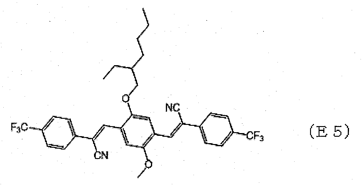
- Compounds (E1) - (E7) may be exemplified as examples in which L consists of substituted aromatic hydrocarbon residue.
-

-

-

-

-
-

-

- Compounds (F1) - (F4) may be exemplified as examples in which R1 is halogenated alkyl group.
-

-

-

-

- Compounds (G1) - (G5) may be exemplified as examples in which L has the structure consisting of the combination of at least two of aromatic ring, heterocycle, and vinylene group.
-

-

-

-

-

- Compounds (H1) - (H7) may be exemplified as examples in which L particularly has the structure consisting of the combination of fused aromatic ring and fused heterocycle among the examples in which L consists of fused heteroaromatic group.
-

-

-

-

-

-

-

- Compounds (I1) - (I3) may be exemplified as other examples.
-

-

-

- Among the compounds of the present invention, the compound having crystallinity is particularly preferred. When the compound of the present invention has crystallinity, a short intermolecular distance facilitates electron transfer. Also, it has the advantage of stable electronic property because of a constant intermolecular distance. In the present invention, the terms "crystalline" and "have crystallinity" mean that second or higher order reflection may be substantially observed in X-ray diffraction (XRD) measurement.
As described below, the compound of the present invention may be preferably applied to the organic semiconductor layer in the form of thin-film having the thickness of about 1 µm or less. Accordingly, it is desirable that the compound of the present invention has crystallinity not only in bulk form but also in the form of a thin-film organic semiconductor layer. - Moreover, the compound of the present invention preferably has a symmetry and it is particularly preferable that it has a point symmetry center.
Among the compounds as exemplified above, the compounds with a plane symmetry include the compounds (C1), (C3), (D2) and (H5). The compounds with a point symmetry include the compounds (A1)-(A4), (B1)-(B6), (C2), (C4)-(C7), (D1), (D3)-(D6), (E1)-(E4), (E6), (E7), (F1)-(F4), (G1)-(G4), (H1)-(H7), and (I1)-(I3) - The aforementioned compounds of the present invention have a high carrier mobility, which is 0.01[cm2/V·sec] or more even without removing oxygen and moisture. Also, the compound of the present invention is highly stable against air (oxygen) and moisture and hard to be oxidized.
- The compound of the present invention is soluble in conventional organic solvents as described below. Accordingly, the thin film of the compound of the present invention may be formed by means of coating method such as cast coating, spin coating, screen printing, and inkjet printing using the solution prepared by dissolving the compound of the present invention in appropriate solvent and optionally adding additive.
The solvent is not particularly limited so far as it may dissolve the compound of the present invention to an appropriate concentration. The example of the solvent includes haloalkane solvents such as chloroform and 1,2-dichloroethane; aromatic solvents such as toluene, o-dichlorobenzene, nitrobenzene and m-cresol; N-methylpyrrolidone and carbon disulfide. - One compound or any combination of two or more compounds selected from the compounds of the present invention may be employed. Also, more than one mixed thin films or laminated films may be formed by using organic semiconductor material known in the art such as pentacene, thiophene oligomer and fullerene together with the compound of the present invention.
- The compound of the present invention may be synthesized by means of any methods known in the art of organic synthesis. Particular methods include bromination, cyanizaiton and aldehyde formation. Knoevenagel condensation reaction is preferably carried out as the final step of the synthesis since the yield of 70% or more may be achieved.
- As mentioned above, the compounds of the present invention are soluble in conventional organic solvents as well as they have stability against air and moisture. Accordingly, the organic semiconductor layer for organic thin-film transistors having superior properties and high reliability may be formed with coating process by using simple device, although it may also be formed on substrate by vacuum sputtering process.
-
Fig. 1 shows a schematic cross sectional view of one of the organic thin-film transistors having the organic semiconductor layer consisting of the organic semiconductor material of the present invention.
The organic thin-film transistor 10 (hereinafter, it may be abbreviated to "transistor 10"), has the structure in which agate electrode 2, agate insulator layer 3, and anorganic semiconductor layer 4 are laminated on asubstrate 1 in that order, and a pair of asource electrode 5 and adrain electrode 6 are formed on theorganic semiconductor layer 4. The structure shown here is one embodiment of the organic thin-film transistor using the organic semiconductor material of the present invention. The organic semiconductor material of the present invention may be applicable not only to the organic thin-film transistor as shown inFig. 1 , but also to any organic thin-film transistors including the one as shown inFig. 2 . - The
substrate 1 is for ensuring the self-supporting property of thetransistor 10. The material used for thesubstrate 1 is not particularly limited and various substrates such as the one made of glass, resins and semiconductor materials such as Si may be preferably employed. The Si substrate is preferably employed from the viewpoint of workability and the mechanical strength of the substrate. In the field of electronic paper and the like, highly flexible resins such as polyethylene naphthalate (PEN) may be preferably employed as thesubstrate 1. Furthermore, in the present embodiment, thesubstrate 1 and thegate electrode 2 are formed by using different materials, however, from the viewpoint of the self-supporting property of thetransistor 10, thegate electrode 2 having the thickness sufficient to be a self-supporting film (self-supporting layer) may be employed so that it may act as thesubstrate 1 as well. - The
gate electrode 2 is used for controlling the source-drain current. The material used for thegate electrode 2 is not particularly limited as long as it is conductive. For example, metals such as chromium (Cr), tantalum (Ta), titanium (Ti), copper (Cu), aluminum (Al), molybdenum (Mo), tungsten (W), nickel (Ni), gold (Au), palladium (Pd), platinum (Pt), silver (Ag), tin (Sn), lithium (Li) and calcium (Ca); oxides of these metals; indium tin oxide (ITO) and zinc oxide (ZnO); conductive polymers known in the art such as conductive polyaniline, conductive polypyrrole and conductive polythiazyl may preferably be used as the material for thegate electrode 2.
In case that thesubstrate 1 is employed, the thickness of thegate electrode 2 is not particularly limited, which is typically from 10 nm to 150 mm.
On the other hand, if thegate electrode 2 also serves as the substrate, the thickness of thegate electrode 2 is preferably from 10 µm to 0.5 mm to ensure sufficient self-supporting property. - The
gate insulator layer 3 is formed between thegate electrode 2 and theorganic semiconductor layer 4. The material used for thegate insulator layer 3 is not limited so far as it has the aforementioned function. In particular, thegate insulator layer 3 may be the insulator layer consisting of at least one of metal oxide film such as silicon oxide (SiO2) aluminum oxide (Al2O3) and tantulum oxide (Ta2O5); organic compound such as polyvinylphenol, polyimide, polyvinyl alcohol, polyethylene, polyethyleneterephthalate, polyvinylidene fluoride, polymethylmethacrylate, polycarbonate, polyethylene fluoride, polystyrene, polyxylylene, cellulose, pullulan and Cytop™. Especially, when Si substrate which is preferred when thegate electrode 2 also serves as the substrate is used as thegate electrode 2, SiO2 formed by oxidizing its surface may be used as thegate insulator layer 3.
The thickness of thegate insulator layer 3 is not particularly limited so far as electronic insulation between thegate electrode 2 and thesource electrode 5, which is typically from 100 to 1000 nm. - The
organic semiconductor layer 4 consists of the organic semiconductor material of the present invention. For forming theorganic semiconductor layer 4 on thegate insulator layer 3, any film formation (deposition) processes known in the art may employed without limitation. The example of the process includes the process in which theorganic semiconductor layer 4 is formed by coating the solution prepared by dissolving the compound of the present invention in appropriate solvent by means of the coating method known in the art such as cast coating, spin coating, screen printing, inkjet printing and ablation (hereinafter, abbreviated to "coating process"); and gas phase film formation process such as vacuum deposition. - As mentioned above, the advantage of the coating process is that cost-reduction and mass-production may be easily achieved since it may be carried out by simple facilities. In the coating process, the solvent is not particularly limited so far as it may dissolve the compound of the present invention to an appropriate concentration. The example of the solvent includes haloalkyl solvents such as chloroform and 1,2-dichloroethane; aromatic solvents such as toluene, o-dichlorobenzene, nitrobenzene and m-cresol; N-methylpyrrolidone and carbon disulfide.
Most of the compounds of the present invention are soluble in general organic solvents. For example, CF3CN-DSB may be favorably coated by dissolving in chloroform or toluene. - Although the cost required for the gas-phase deposition process may be higher than that for the coating process, the compound of the present invention contained in the
organic semiconductor layer 4 tends to be more crystalline. Accordingly, the transistor of higher performance may be fabricated. Among the gas-phase deposition processes, the vacuum deposition process is particularly preferable from the viewpoint of the film quality. - The thickness of the
organic semiconductor layer 4 is not particularly limited. However, the performance of the transistor obtained strongly depend on the thickness of the active layer consisting of the organic semiconductor. The thickness of theorganic semiconductor layer 4 depends on the organic semiconductor, which is generally 1 µm or less, particularly preferably from 10 to 300 nm. - The
source electrode 5 and thedrain electrode 6 are a pair of electrodes formed on theorganic semiconductor layer 4. Current may be supplied from thesource electrode 5 to thedrain electrode 6 via theorganic semiconductor layer 4. The material used for thesource electrode 5 and thedrain electrode 6 is not particularly limited so far as it is conductive, which includes the materials similar to those used for theaforementioned gate electrode 2. Among those materials, the material having small resistance on the surface in contact with theorganic semiconductor layer 4 is preferred. The example of such material includes Cu, Ag, Pt, Au and Au, which is chemically stable and catalytically inert is particularly preferred.
The example of the process for forming such electrodes includes the process in which the electrode formation is carried out by vacuum deposition or sputtering of the aforementioned material through a shadow mask located on the organic semiconductor layer; the process in which the thin-film of the aforementioned material formed by vacuum deposition or sputtering is shaped by photolithographic method or lift-off method known in the art; thermal transfer of metal foil; and etching the thin-film of the aforementioned material using resist formed by inkjet printing and the like. In addition, the examples of the process also include the process in which the electrode formation is carried out by coating a solution or a dispersion of conductive polymer, or a dispersion of conductive microparticulate by direct inkjet printing on a certain pattern; the process in which electrode formation is carried out by lithography and laser ablation of the coated film of the aforementioned material; and the like. - The present invention will be illustrated by examples in more detail. However, the scope of the present invention is not intended to be limited by the examples as described below.
- The reagents used are as follows:
- Reagents
- 4-Trifluoromethylphenylacetonitrile (Tokyo Chemical Industry Co., Ltd.)
- 4-Methylphenylacetonitrile (Tokyo Chemical Industry Co., Ltd.)
- Terephthalaldehyde (Tokyo Chemical Industry Co., Ltd.)
- 2,5'-Bithiophenedialdehyde (synthesized from 2,5-dibromothiophene, butyl lithium and dimethyl formamide)
- 2,6-Thienothiophenedialdehyde (synthesized from 2,6-dibromothienothiophene, butyl lithium and dimethyl formamide)
- Biphenyl-2,2'-dicarboxamide (Tokyo Chemical Industry Co., Ltd.)
- 2,5-Thiophenedialdehyde (synthesized from 2,5-dibromothiophene, butyl lithium and dimethyl formamide)
- 4-Fluorophenylacetonitrile (Tokyo Chemical Industry Co., Ltd.)
- Sodium ethoxide (Wako Pure Chemical Industries Ltd.)
- Potassium t-butoxide (Wako Pure Chemical Industries Ltd.)
- 4-Perfluorohexylphenylacetonitrile (synthesized from iodotoluene and perfluorohexyl iodide)
- 2,5-Difluoroterephthalaldehyde (synthesized from difluorodibromobenzene)
- Using a 50 mL round bottomed flask, 740 mg of 4-trifluoromethylphenylacetonitrile (2 mmol) and 268 mg of terephthalaldehyde (1 mmol) were dissolved in 5 mL of ethanol and 15 mL of DMF with stirring under nitrogen atmosphere. To the solution, an ethanol solution (1 mL) of 14 mg of sodium ethoxide (0.2 mmol) was added dropwise at room temperature under magnetic stirring. After the mixture was stirred for an additional 2 hours, methanol was added, and the resulting crystal was collected by suction filtration. The crystal was thoroughly washed with methanol and dried under reduced pressure in a desiccator to give a crude product. The crude product was recrystallized from chloroform to give the organic semiconductor material 1: (2Z,2'Z)-3,3'-(1,4-phenylene)bis(2-(4-trifluoromethyl)phenylacrylonitrile) (abbrev.: CF3CN-DSB, compound (Al), yellow crystal). Yield: 775 mg (80%).
- A silicon wafer with 300 nm of thermally oxidized silicon dioxide film (SUMCO CORPORATION, 1×1 cm (area: 1cm2), thickness: 525 µm) was used as a gate electrode and a gate insulator layer. A organic semiconductor layer was formed by vacuum deposition (deposition conditions were as follows. pressure: ca. 4.0×10⁻⁶ torr,-deposition rate: 0.5 nm/min, substrate temperature: room temperature (ca. 25°C)) of the
organic semiconductor material 1 under the condition which afforded the film thickness of ca. 50 nm on top of the silicon dioxide film.
A source electrode and a drain electrode of Au having the thickness of ca. 30 nm was formed by vacuum deposition using shadow masks, by which an organicthin film transistor 1 according to Example 1 having the structure as shown inFig. 1 was fabricated. Channel length (L) and channel width (W) of the source and the drain electrodes are 20 µm and 2 mm, respectively. - Using a 100 mL round bottomed flask, 152.2 mg of 2,5'-bithiophenedialdehyde (0.5 mmol) and 185.2 mg of 4-trifluoromethylphenylacetonitrile (1.0 mmol) were dissolved in 7.0 mL of ethanol and 48.0 mL of DMF with stirring under nitrogen atmosphere. To the solution, an ethanol solution (1.0 mL) of 3.4 mg of sodium ethoxide (0.05 mmol) was added dropwise at room temperature under magnetic stirring. After the mixture was stirred for an additional 1 hour and cooled to 0 °C, methanol was added, and the resulting crystal was collected by suction filtration. The crystal was thoroughly washed with methanol and dried under reduced pressure in a desiccator to give a crude product. The crude product was recrystallized from chloroform to give the organic semiconductor material 2: (2Z,2'Z)-3,3'-(5,5'-bithiophene)bis(2-(4-trifluoromethyl)phenylacrylonitrile) (abbrev.: CF3CN-DS2T, compound (C2), red crystal). Yield: 261.9 mg (82%).
- An organic thin-
film transistor 2 according to Example 2 having the structure as shown inFig. 1 was obtained according to the procedure similar to that of Example 1 except that theorganic semiconductor material 2 was used instead of theorganic semiconductor material 1. - Using a 100 mL round bottomed flask, 98.1 mg of 2,6-thienothiophenedialdehyde (0.5 mmol) and 185.2 mg of 4-trifluoromethylphenylacetonitrile (1.0 mmol) were dissolved in 5.0 mL of ethanol and 30.0 mL of DMF with stirring under nitrogen atmosphere. To the solution, an ethanol solution (1.0 mL) of 3.4 mg of sodium ethoxide (0.05 mmol) was added dropwise at room temperature under magnetic stirring. After the mixture was stirred for an additional 1 hour and cooled to 0 °C, methanol was added, and the resulting crystal was collected by suction filtration. The crystal was thoroughly washed with methanol and dried under reduced pressure in a desiccator to give a crude product. The crude product was recrystallized from chloroform to give the organic semiconductor material 3: (2Z,2'Z)-3,3'-(2,5-thieno[3,2-b]thiophene)bis(2-(4-trifluoromethyl)phenylacry lonitrile) (abbrev.: CF3CN-DSTT, compound (D1), orange crystal). Yield: 225.5 mg (85%); MS(FAB+) m/z = 530(M+).
- An organic
thin film transistor 3 according to Example 3 having the structure as shown inFig. 1 was obtained according to the procedure similar to that of Example 1 except that theorganic semiconductor material 3 was used instead of theorganic semiconductor material 1. - Using a 30 mL round bottomed flask, 67.1 mg of terephthalaldehyde (0.5 mmol) and 435.2 mg of acetonitrile derivative (1.0 mmol) were dissolved in ethanol (11 mL) with stirring under nitrogen atmosphere. To the solution, an ethanol solution (1.0 mL) of 3.4 mg of sodium ethoxide (0.05 mmol) was added dropwise at room temperature under magnetic stirring. After the mixture was stirred for an additional 1 hour and cooled to 0 °C, methanol was added, and the resulting crystal was collected by suction filtration. The crystal was thoroughly washed with methanol and dried under reduced pressure in a desiccator to give a crude product. The crude product was recrystallized from chloroform to give the organic semiconductor material 4: (2Z,2'Z)-3,3'-(1,4-phenylene)bis(2-(4-perfluorohexyl)phenylacrylonitrile) (abbrev.: C6F13CN-DSB, compound (F2)). Yield: 328.3 mg (70%).
- An organic
thin film transistor 4 according to Example 4 having the structure as shown inFig. 1 was obtained according to the procedure similar to that of Example 1 except that theorganic semiconductor material 4 was used instead of theorganic semiconductor material 1. - Using a 30 mL round bottomed flask, 70.1 mg of 2,5-thiophenedialdehyde (0.5 mmol) and 185.2 mg of 4-trifluoromethylphenylacetonitrile (1.0 mmol) were dissolved in 1.0 mL of ethanol and 4.0 mL of DMF with stirring under nitrogen atmosphere. To the solution, an ethanol solution (1.0 mL) of 3.4 mg of sodium ethoxide (0.05 mmol) was added dropwise at room temperature under magnetic stirring. After the mixture was stirred for an additional 1 hour, water was added followed by the addition of saturated aqueous sodium chloride. The mixture was extracted with chloroform (3 times). After drying, the solvent was evaporated. The crude product was recrystallized from hexane-chloroform to give (2Z,2'Z)-3,3'(2,5-thiophene)bis(2-(4-trifluorornethyl)phenylacrylonitrile) (abbrev.: CF3CN-DSIT, compound (C1), orange crystal). Yield: 217.0 mg (91%).
- An organic
thin film transistor 5 according to Example 5 having the structure as shown inFig. 1 was obtained according to the procedure similar to that of Example 1 except that theorganic semiconductor material 5 was used instead of theorganic semiconductor material 1. - Using a 50 mL round bottomed flask, 186 mg of 4-trifluoromethylphenylacetonitrile (1.0 mmol) and 100 mg of biphenyl-2,2'-dicarboxaldehyde (0.5 mmol) were dissolved in 5 mL of ethanol and 15 mL of THF with stirring under nitrogen atmosphere. To the solution, an ethanol solution (2 mL) of 11 mg of potassium t-butoxide (0.1 mmol) was added dropwise at 0°C with magnetic stirring. After the mixture was stirred for an additional 2 hours at room temperature, methanol was added. The resulting crystal was collected by suction filtration. The crystal was thoroughly washed with methanol and dried under reduced pressure in a desiccator to give a crude product. The crude product was recrystallized from chloroform to give an organic semiconductor material 6: (2Z,2'Z)-3,3'-(4,4'-biphenyl)bis(2-(4-trifluoromethyl)phenylacrylonitrile) (abbrev.: CF3CN-DSBP, compound (A2), pale blue crystal). Yield: 230 mg (90%).
- An organic
thin film transistor 6 according to Example 6 having the structure as shown inFig. 1 was obtained according to the procedure similar to that of Example 1 except that theorganic semiconductor material 6 was used instead of theorganic semiconductor material 1. - Using a 100 mL round bottomed flask, 170.1 mg of difluoroaldehyde (1.0 mmol) and 370.3 mg of 4-trifluoromethylphenylacetonitrile (2.0 mmol), were dissolved in ethanol (49 mL) under nitrogen atmosphere. To the solution, an ethanol solution (1 mL) of 6.8 mg of sodium ethoxide (2.0 mmol) was added dropwise at room temperature with magnetic stirring. After the mixture was stirred for an additional 1 hour and cooled to 0 °C, methanol was added. The resulting crystal was collected by suction filtration. The crystal was thoroughly washed with methanol and dried under reduced pressure in a desiccator to give 469.1 mg of crude product of difluorinated distyryl derivative (ca. 93%). The crude product was recrystallized from hexane/chloroform to give (2Z,2'Z)-3,3'-(2,5-difluoro)bis(2-(4-trifluoromethyl)phenylacrylonitrile) (abbrev.: CF3CN-DSBF2, compound (E6), yellow crystal). Yield: 395.7 mg (78%).
- An organic thin film transistor 7 according to Example 7 having the structure as shown in
Fig. 1 was obtained according to the procedure similar to that of Example 1 except that the organic semiconductor material 7 was used instead of theorganic semiconductor material 1. - An organic semiconductor material 8: (2Z,2'Z)-3,3'-(1,4-phenylene)bis(2-(4-methyl)phenylacrylonitrile) (abbrev.: CH3CN-DSB) was synthesized according to the procedure similar to that of Example 1 except that the 4-methylphenylacetonitrile was used instead of 4-trifluoromethylphenylacetonitrile.
- An organic
thin film transistor 8 according to Comparative example 1 having the structure as shown inFig. 1 was obtained according to the procedure similar to that of Example 1 except that theorganic semiconductor material 8 was used instead of theorganic semiconductor material 1. - An organic semiconductor material 9: (2Z,2'Z)-3,3'-(1,4-phenylene)bis(2-(4-fluoro)phenylacrylonitrile) (abbrev.: FCN-DSB) was synthesized according to the procedure similar to that of Example 1 except that the 4-fluorophenylacetonitrile was used instead of 4-trifluoromethylphenylacetonitrile.
- An organic thin film transistor 9 according to Comparative example 2 having the structure as shown in
Fig. 1 was obtained according to the procedure similar to that of Example 1 except that the organic semiconductor material 9 was used instead of theorganic semiconductor material 1. - Characterization of output characteristics and transfer characteristics of organic thin-film transistors 1-9 fabricated under vacuum (10-5 torr or less) was carried out using Keithley Model 2612A Dual-Channel System SourceMeter® by applying a voltage of -100 V between the source- and drain electrodes of each organic thin-film transistor and varying the gate voltage from -100 V to 100 V.
As a representative example, the output characteristics and the transfer characteristics of organic thin-film transistor 2 (Example 2) are shown inFig. 3 and Fig.4 , respectively.
The ratio of maximum current value and minimum current value observed in the characterization of the transfer characteristic was defined as the ON/OFF ratio of each organic thin-film transistor. The carrier mobility of each organic thin-film transistor was estimated from the saturated region of the transfer characteristic. The ON/OFF ratio and the carrier mobility of the organic thin-film transistor are shown in Table 1. -
Table 1 organic thin-film transistor organic semiconductor material ON/OFF ratio carrier mobility [cm2/V·sec] polarity Example 1 organic thin- film transistor 1CF3CN- DSB 106 0.13 n Example 2 organic thin- film transistor 2CF3CN- DS2T 106 0.08 n Example 3 organic thin- film transistor 3CF3CN- DSTT 106 0.05 n Example 4 organic thin-film transistor 4 C6F13CN- DSB 103 0.001 n Example 5 organic thin- film transistor 5CF3CN- DS1T 106 0.03 n Example 6 organic thin- film transistor 6CF3CN- DSBP 104 0.001 n Example 7 organic thin-film transistor 7 CF3CN- DSBF 2106 0.13 n Comparative example 1 organic thin- film transistor 8CH3CN-DSB - - - Comparative example 2 organic thin-film transistor 9 FCN-DSB - - - - The organic semiconductor material 1: (2Z,2'Z)-3,3'-(1,4-phenylene)bis(2-(4-trifluoromethyl)phenylacrylonitrile) (abbrev.: CF3CN-DSB, compound (A1)) was synthesized according to the procedure similar to that of Examples 1.
- As a substrate, a PEN film (thickness: 100 µm) was used instead of a silicon wafer with thermal oxidized film, on which a gate electrode was formed by vacuum deposition of Au (40 nm)/Ti (5 nm). As a gate insulator film, an insulator film of polyimide (capacitance: C=4.5 nF/cm2) having the thickness of ca. 600 nm was formed by spin-coating of a precursor solution of the polyimide followed by heat treatment. An organic
thin film transistor 10 according to Example 8 having the structure as shown inFig. 2 was fabricated by depositing theorganic semiconductor layer 1 having the thickness of ca. 30 nm on top of the polyimide insulator film under vacuum, follow by depositing Au (thickness: 40 nm, L=20 µm, W=2 mm) as the source and the drain electrodes. The output characteristics and the transfer characteristics of organic thin-film transistor 10 are shown inFig. 5 and Fig.6 , respectively. The ON/OFF ratio and the carrier (electron) mobility of the organic thin-film transistor 10 estimated similarly to the aforementioned Examples were 105 and 0.1[cm2/V·sec]; respectively. - The organic semiconductor material 1: (2Z,2'Z)-3,3'-(1,4-phenylene)bis(2-(4-trifluoromethyl)phenylacrylonitrile) (abbrev.: CF3CN-DSB, compound (A1)) was synthesized according to the procedure similar to that of Example 1.
- A silicon wafer with 300 nm of thermally oxidized silicon dioxide film (SUMCO CORPORATION, 1×1 cm (area: 1cm2), thickness: 525 µm) was used as a gate electrode and a gate insulator layer. A organic semiconductor layer was formed by drop casting of the solution of the
organic semiconductor material 1 having the concentration of 1 mg/mL to the surface of the oxidized film.
A source electrode and a drain electrode of Au having the thickness of ca. 30 nm was formed by vacuum deposition using shadow masks, by which an organic thin film transistor 11 according to Example 9 having the structure as shown inFig. 1 was fabricated. Channel length (L) and channel width (W) of the source and the drain electrodes are 20 µm and 2 mm, respectively. The ON/OFF ratio and the carrier (electron) mobility of the organic thin-film transistor 11 estimated similarly to the aforementioned Examples were 103 and 0.0002[cm2/V·sec], respectively. - The organic semiconductor material 1: (2Z,2'Z)-3,3'-(1,4-phenylene)bis(2-(4-trifluoromethyl)phenylacrylonitrile) (abbrev.: CF3CN-DSB, compound (A1)) was synthesized according to the procedure similar to that of Example 1.
- An organic
thin film transistor 12 was obtained according to the procedure similar to that of Example 1 except that the Ag was used instead of Au as the source and the drain electrodes. The source and the drain electrodes were formed by the vacuum deposition process, of which thickness is ca. 30 nm.
The ON/OFF ratio and the carrier (electron) mobility of the organic thin-film transistor 12 estimated similarly to the aforementioned Examples were 106 and 0.20[cm2V·sec], respectively. - The organic
thin film transistor 1 was fabricated according to the procedure similar to that of Example 1 and its atmospheric operation test, atmospheric exposure stability test and characterization of crystallinity were carried out. - Atmospheric operation test (Tests 1-4) of the organic thin-
film transistor 1 as followings were carried out. The characterizations were carried out similarly to those of Example 1 and the like. Characterization of transfer characteristics of organic thin-film transistor 1 was carried out using Keithley Model 2612A Dual-Channel System SourceMeter® by applying a voltage of -100 V between the source- and drain electrodes of each organic thin-film transistor and varying the gate voltage from -100 V to 100 V. The carrier mobility was estimated from the saturated region of the transfer characteristic.
Deterioration rate of the mobility was estimated using the mobility obtained inTest 1 as an initial value. Shift in threshold was estimated from the shift amount from the value estimated inTest 1. - Test 1: The characterization of the organic thin-
film transistor 1 just after fabrication was carried out under vacuum (10-5 torr or less). - Test 2: The organic thin-
film transistor 1 was exposed to the atmosphere afterTest 1, then the characterization was carried out immediately in the atmosphere. - Test 3: The organic thin-
film transistor 1 was exposed to the atmosphere afterTest 2, which was subjected to the characterization every few hours in the atmosphere. The organic thin-film transistor 1 was stored in the dark atmosphere. - Test 4: The characterization of the organic thin-
film transistor 1 afterTest 3 under vacuum (10-5 torr or less). -
Table 2 mobility
µ[cm2/V·s]deterioration rate
Δµ[%]shift in threshold
ΔVth[V]Test 10.085 - - Test 20.050 41 - Test 30.020 76 - Test 40.073 14 7 - Atmospheric exposure stability test of the organic thin-
film transistor 1 was carried out. The organic thin-film transistor 1 was stored in dark atmosphere for a certain period of time, which was subjected to the characterization under vacuum (10-5 torr or less). The characterization was carried out according to the procedure as in Example 11. Results are shown inFig. 8 .
It is seen fromFig. 8 that no significant deterioration in the characteristics is not observed after 30 days of atmospheric exposure. - The crystallinity of the organic semiconductor layer in the organic thin-
film transistor 1 was characterized as follows.
The characterization of the crystallinity was carried out by measuring in-plane and out-of-plane X-ray diffraction (XRD) of the organic semiconductor layer using ATX-GSOR for structure characterization of thin film in BL46XU beamline of synchrotron radiation facility SPring-8. Results are shown inFig. 9 .
Diffraction peaks in each in-plane and out-of-plane XRD profile show that the organic semiconductor layer in the organic thin-film transistor 1 is crystalline thin film. Moreover, fifth and higher order peaks observed in the out-of-plane diffraction profile show that the organic semiconductor layer is highly crystalline. - The organic thin film transistor 7 was fabricated according to the procedure similar to that of Example 7 and its atmospheric operation tests were carried out as follows:
- Test 1: The characterization of the organic thin-film transistor 7 just after fabrication was carried out under vacuum (10-5 torr or less).
- Test 2: The organic thin-film transistor 7 was exposed to the atmosphere after
Test 1, then the characterization was carried out immediately in the atmosphere. - Test 3: The organic thin-film transistor 7 was exposed to the atmosphere after
Test 2, stored in the atmosphere for 24 hours, which was subjected to the characterization in the atmosphere. The organic thin-film transistor 1 was stored in the dark atmosphere. - The organic semiconductor material of the present invention is preferably applicable to the organic semiconductor layer for the organic thin-film-transistor because of its high carrier mobility and chemical stability. Also, the production cost of the organic semiconductor material of the present invention may be reduced since its film may be formed at relatively low temperature as well as using by a simple production process such as a coating process.
The organic thin-film transistor in which the organic semiconductor material is used may be applied to various integrated circuits (IC) because of its large ON/OFF ratio and high response rate. Also, the organic semiconductor material of the present invention may be widely applied to light emitting materials and charge injection materials for organic EL devices, charge conductive materials and organic laser oscillators because of its excellent electronic properties. -
- 1:
- substrate
- 2:
- gate electrode
- 3:
- gate insulator layer
- 4:
- organic semiconductor layer
- 5:
- source electrode
- 6:
- drain electrode
- 10:
- organic thin-film transistor
It is clear from Table 2 and
It is clear from
Claims (14)
- An organic semiconductor material having the structure represented by the general formula (1) shown below:

R1 represents carbonyl group, cyano group or C1-C12 fluorinated alkyl group;
R2 represents halogen atom, cyano group, carbonyl group or acetyl group. - The organic semiconductor material according to claim 1, wherein the compound has crystallinity.
- The organic semiconductor material according to claims 1 or 2, wherein the compound has a symmetric molecular structure.
- The organic semiconductor material according to claim 3, wherein the compound has a point symmetry center.
- The organic semiconductor material according to any one of claims 1 to 4, wherein R1 in the general formula (1) is C1-C6 fluorinated alkyl group.
- The organic semiconductor material according to any one of claims 1 to 4, wherein R1 in the general formula (1) is C1-C3 fluorinated alkyl group.
- The organic semiconductor material according to any one of claims 1 to 6, wherein R2 in the general formula (1) is cyano group.
- The organic semiconductor material according to any one of claims 1 to 7, wherein L in the general formula (1) consists of less than or equal to 4 groups.
- The organic semiconductor material according to any one of claims 1 to 8, wherein L in the general formula (1) has the structure consisting of one or any combination of two or more groups selected from unsubstituted or substituted vinylene group, unsubstituted or substituted benzene residue, unsubstituted or substituted naphthalene residue, unsubstituted or substituted anthracene residue, unsubstituted or substituted thiophene residue, unsubstituted or substituted thienothiophene residue, unsubstituted or substituted furan residue, unsubstituted or substituted pyrrole residue, and unsubstituted or substituted thiazole residue.
- The organic semiconductor material according to claim 9, wherein L in the general formula (1) is unsubstituted benzene residue, unsubstituted thiophene residue or unsubstituted thienothiophene residue.
- An organic thin-film transistor comprising a gate electrode, a gate insulator layer, an organic semiconductor layer, a source electrode and a drain electrode, wherein the organic semiconductor layer consists of the organic semiconductor material according to any one of claims 1 to 10.
- The organic thin-film transistor according to claim 11, wherein the organic semiconductor layer has crystallinity.
- A method for manufacturing an organic thin-film transistor comprising a gate electrode, a gate insulator layer, an organic semiconductor layer, a source electrode and a drain electrode, wherein the organic semiconductor layer is formed by coating of an organic solvent containing the organic semiconductor material according to any one of claims 1 to 10.
- A method for manufacturing an organic thin-film transistor comprising a gate electrode, a gate insulator layer, an organic semiconductor layer, a source electrode and a drain electrode, wherein the organic semiconductor layer is formed by vapor-deposition of the organic semiconductor material according to any one of claims 1 to 10.
Applications Claiming Priority (2)
| Application Number | Priority Date | Filing Date | Title |
|---|---|---|---|
| JP2009053759 | 2009-03-06 | ||
| PCT/JP2010/053577 WO2010101224A1 (en) | 2009-03-06 | 2010-03-04 | Organic semiconductor material and organic thin film transistor |
Publications (3)
| Publication Number | Publication Date |
|---|---|
| EP2405505A1 true EP2405505A1 (en) | 2012-01-11 |
| EP2405505A4 EP2405505A4 (en) | 2013-06-05 |
| EP2405505B1 EP2405505B1 (en) | 2020-03-04 |
Family
ID=42709778
Family Applications (1)
| Application Number | Title | Priority Date | Filing Date |
|---|---|---|---|
| EP10748817.3A Active EP2405505B1 (en) | 2009-03-06 | 2010-03-04 | Organic thin film transistor |
Country Status (4)
| Country | Link |
|---|---|
| US (1) | US8674347B2 (en) |
| EP (1) | EP2405505B1 (en) |
| JP (2) | JP5626806B2 (en) |
| WO (1) | WO2010101224A1 (en) |
Families Citing this family (8)
| Publication number | Priority date | Publication date | Assignee | Title |
|---|---|---|---|---|
| JP2011057638A (en) * | 2009-09-11 | 2011-03-24 | Tokyo Institute Of Technology | Phenylenevinylene compound, and field-effect transistor containing the same |
| CN102477045A (en) * | 2010-11-30 | 2012-05-30 | 中国科学院上海有机化学研究所 | A class of thiophene quinone compounds, their preparation methods, intermediates and their applications |
| JP2014005224A (en) * | 2012-06-22 | 2014-01-16 | Nippon Kayaku Co Ltd | Method of producing aromatic dialdehyde compound and oligovinylenephenylene compound |
| TW201429025A (en) * | 2012-09-28 | 2014-07-16 | 新日鐵住金化學股份有限公司 | Organic thin film solar cell |
| JP5787038B2 (en) * | 2013-01-07 | 2015-09-30 | 富士電機株式会社 | Transparent organic thin film transistor and manufacturing method thereof |
| US9844362B2 (en) | 2015-01-13 | 2017-12-19 | Covidien Lp | Exchangeable core biopsy needle |
| JP6318452B2 (en) * | 2015-01-19 | 2018-05-09 | 富士フイルム株式会社 | Organic thin film transistor and manufacturing method thereof |
| JP6986692B2 (en) * | 2016-03-31 | 2021-12-22 | 日鉄ケミカル&マテリアル株式会社 | Nitrogen-containing heterocyclic alkenyl compounds, organic semiconductor materials and organic semiconductor devices |
Family Cites Families (12)
| Publication number | Priority date | Publication date | Assignee | Title |
|---|---|---|---|---|
| JPH05100451A (en) * | 1991-08-13 | 1993-04-23 | Minolta Camera Co Ltd | Photosensitive body |
| US5380613A (en) * | 1991-08-13 | 1995-01-10 | Minolta Camera Kabushiki Kaisha | Photosensitive member comprising electronattracting compound and hindered phenol compound |
| JPH0659486A (en) | 1992-07-29 | 1994-03-04 | Matsushita Electric Ind Co Ltd | Electrophotographic sensitive body |
| JPH06123986A (en) * | 1992-10-12 | 1994-05-06 | Ricoh Co Ltd | Single layer type electrophotographic photoreceptor |
| JP3629958B2 (en) | 1998-06-26 | 2005-03-16 | 松下電器産業株式会社 | Solenoid drive |
| JP2004214482A (en) | 2003-01-07 | 2004-07-29 | Konica Minolta Holdings Inc | Organic semiconductor materials and organic thin film transistors |
| FR2881745A1 (en) * | 2005-02-08 | 2006-08-11 | Univ Aix Marseille Ii | OLIGOTHIOPHENE DERIVATIVES AND THEIR APPLICATION IN ORGANIC ELECTRONICS |
| JP2007116115A (en) | 2005-09-21 | 2007-05-10 | Mitsubishi Chemicals Corp | Organic semiconductor material and organic field effect transistor |
| CN100585902C (en) | 2005-09-21 | 2010-01-27 | 三菱化学株式会社 | Organic Semiconductor Materials and Organic Field Effect Transistors |
| US7521710B2 (en) | 2006-02-16 | 2009-04-21 | Idemitsu Kosan Co., Ltd. | Organic thin film transistor |
| JP5308164B2 (en) * | 2006-12-04 | 2013-10-09 | 出光興産株式会社 | Organic thin film transistor and organic thin film light emitting transistor |
| JP2011057638A (en) * | 2009-09-11 | 2011-03-24 | Tokyo Institute Of Technology | Phenylenevinylene compound, and field-effect transistor containing the same |
-
2010
- 2010-03-04 JP JP2011502805A patent/JP5626806B2/en not_active Expired - Fee Related
- 2010-03-04 US US13/254,574 patent/US8674347B2/en not_active Expired - Fee Related
- 2010-03-04 EP EP10748817.3A patent/EP2405505B1/en active Active
- 2010-03-04 WO PCT/JP2010/053577 patent/WO2010101224A1/en not_active Ceased
-
2013
- 2013-01-11 JP JP2013003715A patent/JP5553185B2/en not_active Expired - Fee Related
Also Published As
| Publication number | Publication date |
|---|---|
| US20120001162A1 (en) | 2012-01-05 |
| JP5626806B2 (en) | 2014-11-19 |
| JPWO2010101224A1 (en) | 2012-09-10 |
| EP2405505B1 (en) | 2020-03-04 |
| WO2010101224A1 (en) | 2010-09-10 |
| JP2013107891A (en) | 2013-06-06 |
| US8674347B2 (en) | 2014-03-18 |
| EP2405505A4 (en) | 2013-06-05 |
| JP5553185B2 (en) | 2014-07-16 |
Similar Documents
| Publication | Publication Date | Title |
|---|---|---|
| US8624232B2 (en) | Ambipolar polymeric semiconductor materials and organic electronic devices | |
| US8674347B2 (en) | Organic semiconductor material and organic thin-film transistor | |
| US7355199B2 (en) | Substituted anthracenes and electronic devices containing the substituted anthracenes | |
| JP4958119B2 (en) | Novel condensed polycyclic aromatic compound, method for producing the same, and use thereof | |
| KR101410150B1 (en) | Field-effect transistor | |
| CN102714276B (en) | Organic semiconductor materials, organic semiconductor thin films, and organic thin film transistors | |
| JP5308532B2 (en) | Organic semiconductor material, organic semiconductor thin film and organic thin film transistor | |
| EP2213692A1 (en) | Polymer Semiconductors with High Mobility | |
| JP7514258B2 (en) | Polycyclic aromatic compounds | |
| WO2012157474A1 (en) | Compound, field effect transistor, method for manufacturing field effect transistor, solar cell, organic light-emitting element, composition, array for display devices, and display device | |
| JP6592758B2 (en) | Novel condensed polycyclic aromatic compounds and uses thereof | |
| JP2015199716A (en) | Polycyclic fused ring compounds, organic semiconductor materials, organic semiconductor devices, and organic transistors | |
| US20050277760A1 (en) | Device with small molecular thiophene compound having divalent linkage | |
| US20050276981A1 (en) | Device with small molecular thiophene compound | |
| US20090159876A1 (en) | Organic semiconductor material and organic field effect transistor | |
| JP5392706B2 (en) | Organic semiconductor material and organic thin film transistor | |
| JP2008100980A (en) | Organic semiconductor compound, organic semiconductor thin film, organic semiconductor coating liquid, organic thin film transistor, bis (benzo [4,5] thieno) [2,3-b: 3′2′-e] [1,4] dithiine production method, And bis (benzo [4,5] thieno) [2,3-b: 2′3′-e] [1,4] dithiin | |
| JP7489996B2 (en) | Polycyclic aromatic compounds | |
| JP4934995B2 (en) | Organic semiconductor material, organic semiconductor structure and organic semiconductor device | |
| JP2011093827A (en) | Novel compound, field-effect transistor, and solar cell | |
| JP2014177405A (en) | Compound, field effect transistor, method of manufacturing the same, solar cell, organic light-emitting element, composition, array for display device, and display device | |
| JP2014141416A (en) | Compound, field effect transistor, method of manufacturing the same, solar cell, organic light-emitting element, composition, array for display device, and display device | |
| JP2014177403A (en) | Compound, field effect transistor, method of manufacturing the same, solar cell, organic light-emitting element, composition, array for display device, and display device | |
| JP2009152382A (en) | Organic transistor |
Legal Events
| Date | Code | Title | Description |
|---|---|---|---|
| PUAI | Public reference made under article 153(3) epc to a published international application that has entered the european phase |
Free format text: ORIGINAL CODE: 0009012 |
|
| 17P | Request for examination filed |
Effective date: 20111005 |
|
| AK | Designated contracting states |
Kind code of ref document: A1 Designated state(s): AT BE BG CH CY CZ DE DK EE ES FI FR GB GR HR HU IE IS IT LI LT LU LV MC MK MT NL NO PL PT RO SE SI SK SM TR |
|
| DAX | Request for extension of the european patent (deleted) | ||
| A4 | Supplementary search report drawn up and despatched |
Effective date: 20130507 |
|
| RIC1 | Information provided on ipc code assigned before grant |
Ipc: C07D 495/04 20060101ALI20130429BHEP Ipc: C07C 255/35 20060101ALI20130429BHEP Ipc: C07D 333/24 20060101ALI20130429BHEP Ipc: C07C 255/37 20060101ALI20130429BHEP Ipc: H01L 51/40 20060101ALI20130429BHEP Ipc: C07C 255/40 20060101ALI20130429BHEP Ipc: C07C 255/34 20060101ALI20130429BHEP Ipc: H01L 29/786 20060101ALI20130429BHEP Ipc: H01L 51/30 20060101AFI20130429BHEP Ipc: H01L 51/05 20060101ALI20130429BHEP |
|
| 17Q | First examination report despatched |
Effective date: 20151109 |
|
| STAA | Information on the status of an ep patent application or granted ep patent |
Free format text: STATUS: EXAMINATION IS IN PROGRESS |
|
| GRAP | Despatch of communication of intention to grant a patent |
Free format text: ORIGINAL CODE: EPIDOSNIGR1 |
|
| STAA | Information on the status of an ep patent application or granted ep patent |
Free format text: STATUS: GRANT OF PATENT IS INTENDED |
|
| RIC1 | Information provided on ipc code assigned before grant |
Ipc: H01L 51/30 20060101AFI20190812BHEP |
|
| INTG | Intention to grant announced |
Effective date: 20190916 |
|
| GRAS | Grant fee paid |
Free format text: ORIGINAL CODE: EPIDOSNIGR3 |
|
| GRAA | (expected) grant |
Free format text: ORIGINAL CODE: 0009210 |
|
| STAA | Information on the status of an ep patent application or granted ep patent |
Free format text: STATUS: THE PATENT HAS BEEN GRANTED |
|
| AK | Designated contracting states |
Kind code of ref document: B1 Designated state(s): AT BE BG CH CY CZ DE DK EE ES FI FR GB GR HR HU IE IS IT LI LT LU LV MC MK MT NL NO PL PT RO SE SI SK SM TR |
|
| REG | Reference to a national code |
Ref country code: GB Ref legal event code: FG4D |
|
| REG | Reference to a national code |
Ref country code: CH Ref legal event code: EP |
|
| REG | Reference to a national code |
Ref country code: AT Ref legal event code: REF Ref document number: 1241384 Country of ref document: AT Kind code of ref document: T Effective date: 20200315 |
|
| REG | Reference to a national code |
Ref country code: DE Ref legal event code: R096 Ref document number: 602010063340 Country of ref document: DE |
|
| REG | Reference to a national code |
Ref country code: IE Ref legal event code: FG4D |
|
| PG25 | Lapsed in a contracting state [announced via postgrant information from national office to epo] |
Ref country code: FI Free format text: LAPSE BECAUSE OF FAILURE TO SUBMIT A TRANSLATION OF THE DESCRIPTION OR TO PAY THE FEE WITHIN THE PRESCRIBED TIME-LIMIT Effective date: 20200304 Ref country code: NO Free format text: LAPSE BECAUSE OF FAILURE TO SUBMIT A TRANSLATION OF THE DESCRIPTION OR TO PAY THE FEE WITHIN THE PRESCRIBED TIME-LIMIT Effective date: 20200604 |
|
| REG | Reference to a national code |
Ref country code: NL Ref legal event code: MP Effective date: 20200304 |
|
| PG25 | Lapsed in a contracting state [announced via postgrant information from national office to epo] |
Ref country code: LV Free format text: LAPSE BECAUSE OF FAILURE TO SUBMIT A TRANSLATION OF THE DESCRIPTION OR TO PAY THE FEE WITHIN THE PRESCRIBED TIME-LIMIT Effective date: 20200304 Ref country code: SE Free format text: LAPSE BECAUSE OF FAILURE TO SUBMIT A TRANSLATION OF THE DESCRIPTION OR TO PAY THE FEE WITHIN THE PRESCRIBED TIME-LIMIT Effective date: 20200304 Ref country code: BG Free format text: LAPSE BECAUSE OF FAILURE TO SUBMIT A TRANSLATION OF THE DESCRIPTION OR TO PAY THE FEE WITHIN THE PRESCRIBED TIME-LIMIT Effective date: 20200604 Ref country code: GR Free format text: LAPSE BECAUSE OF FAILURE TO SUBMIT A TRANSLATION OF THE DESCRIPTION OR TO PAY THE FEE WITHIN THE PRESCRIBED TIME-LIMIT Effective date: 20200605 Ref country code: HR Free format text: LAPSE BECAUSE OF FAILURE TO SUBMIT A TRANSLATION OF THE DESCRIPTION OR TO PAY THE FEE WITHIN THE PRESCRIBED TIME-LIMIT Effective date: 20200304 |
|
| REG | Reference to a national code |
Ref country code: LT Ref legal event code: MG4D |
|
| PG25 | Lapsed in a contracting state [announced via postgrant information from national office to epo] |
Ref country code: NL Free format text: LAPSE BECAUSE OF FAILURE TO SUBMIT A TRANSLATION OF THE DESCRIPTION OR TO PAY THE FEE WITHIN THE PRESCRIBED TIME-LIMIT Effective date: 20200304 |
|
| PG25 | Lapsed in a contracting state [announced via postgrant information from national office to epo] |
Ref country code: RO Free format text: LAPSE BECAUSE OF FAILURE TO SUBMIT A TRANSLATION OF THE DESCRIPTION OR TO PAY THE FEE WITHIN THE PRESCRIBED TIME-LIMIT Effective date: 20200304 Ref country code: IS Free format text: LAPSE BECAUSE OF FAILURE TO SUBMIT A TRANSLATION OF THE DESCRIPTION OR TO PAY THE FEE WITHIN THE PRESCRIBED TIME-LIMIT Effective date: 20200704 Ref country code: SK Free format text: LAPSE BECAUSE OF FAILURE TO SUBMIT A TRANSLATION OF THE DESCRIPTION OR TO PAY THE FEE WITHIN THE PRESCRIBED TIME-LIMIT Effective date: 20200304 Ref country code: EE Free format text: LAPSE BECAUSE OF FAILURE TO SUBMIT A TRANSLATION OF THE DESCRIPTION OR TO PAY THE FEE WITHIN THE PRESCRIBED TIME-LIMIT Effective date: 20200304 Ref country code: PT Free format text: LAPSE BECAUSE OF FAILURE TO SUBMIT A TRANSLATION OF THE DESCRIPTION OR TO PAY THE FEE WITHIN THE PRESCRIBED TIME-LIMIT Effective date: 20200729 Ref country code: SM Free format text: LAPSE BECAUSE OF FAILURE TO SUBMIT A TRANSLATION OF THE DESCRIPTION OR TO PAY THE FEE WITHIN THE PRESCRIBED TIME-LIMIT Effective date: 20200304 Ref country code: LT Free format text: LAPSE BECAUSE OF FAILURE TO SUBMIT A TRANSLATION OF THE DESCRIPTION OR TO PAY THE FEE WITHIN THE PRESCRIBED TIME-LIMIT Effective date: 20200304 Ref country code: ES Free format text: LAPSE BECAUSE OF FAILURE TO SUBMIT A TRANSLATION OF THE DESCRIPTION OR TO PAY THE FEE WITHIN THE PRESCRIBED TIME-LIMIT Effective date: 20200304 Ref country code: CZ Free format text: LAPSE BECAUSE OF FAILURE TO SUBMIT A TRANSLATION OF THE DESCRIPTION OR TO PAY THE FEE WITHIN THE PRESCRIBED TIME-LIMIT Effective date: 20200304 |
|
| REG | Reference to a national code |
Ref country code: CH Ref legal event code: PL |
|
| REG | Reference to a national code |
Ref country code: AT Ref legal event code: MK05 Ref document number: 1241384 Country of ref document: AT Kind code of ref document: T Effective date: 20200304 |
|
| REG | Reference to a national code |
Ref country code: DE Ref legal event code: R097 Ref document number: 602010063340 Country of ref document: DE |
|
| REG | Reference to a national code |
Ref country code: BE Ref legal event code: MM Effective date: 20200331 |
|
| PG25 | Lapsed in a contracting state [announced via postgrant information from national office to epo] |
Ref country code: LU Free format text: LAPSE BECAUSE OF NON-PAYMENT OF DUE FEES Effective date: 20200304 Ref country code: MC Free format text: LAPSE BECAUSE OF FAILURE TO SUBMIT A TRANSLATION OF THE DESCRIPTION OR TO PAY THE FEE WITHIN THE PRESCRIBED TIME-LIMIT Effective date: 20200304 |
|
| PLBE | No opposition filed within time limit |
Free format text: ORIGINAL CODE: 0009261 |
|
| STAA | Information on the status of an ep patent application or granted ep patent |
Free format text: STATUS: NO OPPOSITION FILED WITHIN TIME LIMIT |
|
| PG25 | Lapsed in a contracting state [announced via postgrant information from national office to epo] |
Ref country code: DK Free format text: LAPSE BECAUSE OF FAILURE TO SUBMIT A TRANSLATION OF THE DESCRIPTION OR TO PAY THE FEE WITHIN THE PRESCRIBED TIME-LIMIT Effective date: 20200304 Ref country code: AT Free format text: LAPSE BECAUSE OF FAILURE TO SUBMIT A TRANSLATION OF THE DESCRIPTION OR TO PAY THE FEE WITHIN THE PRESCRIBED TIME-LIMIT Effective date: 20200304 Ref country code: IT Free format text: LAPSE BECAUSE OF FAILURE TO SUBMIT A TRANSLATION OF THE DESCRIPTION OR TO PAY THE FEE WITHIN THE PRESCRIBED TIME-LIMIT Effective date: 20200304 Ref country code: IE Free format text: LAPSE BECAUSE OF NON-PAYMENT OF DUE FEES Effective date: 20200304 Ref country code: LI Free format text: LAPSE BECAUSE OF NON-PAYMENT OF DUE FEES Effective date: 20200331 Ref country code: CH Free format text: LAPSE BECAUSE OF NON-PAYMENT OF DUE FEES Effective date: 20200331 |
|
| 26N | No opposition filed |
Effective date: 20201207 |
|
| PG25 | Lapsed in a contracting state [announced via postgrant information from national office to epo] |
Ref country code: PL Free format text: LAPSE BECAUSE OF FAILURE TO SUBMIT A TRANSLATION OF THE DESCRIPTION OR TO PAY THE FEE WITHIN THE PRESCRIBED TIME-LIMIT Effective date: 20200304 Ref country code: SI Free format text: LAPSE BECAUSE OF FAILURE TO SUBMIT A TRANSLATION OF THE DESCRIPTION OR TO PAY THE FEE WITHIN THE PRESCRIBED TIME-LIMIT Effective date: 20200304 Ref country code: BE Free format text: LAPSE BECAUSE OF NON-PAYMENT OF DUE FEES Effective date: 20200331 |
|
| PG25 | Lapsed in a contracting state [announced via postgrant information from national office to epo] |
Ref country code: FR Free format text: LAPSE BECAUSE OF NON-PAYMENT OF DUE FEES Effective date: 20200504 |
|
| PGFP | Annual fee paid to national office [announced via postgrant information from national office to epo] |
Ref country code: GB Payment date: 20220324 Year of fee payment: 13 Ref country code: DE Payment date: 20220209 Year of fee payment: 13 |
|
| PG25 | Lapsed in a contracting state [announced via postgrant information from national office to epo] |
Ref country code: TR Free format text: LAPSE BECAUSE OF FAILURE TO SUBMIT A TRANSLATION OF THE DESCRIPTION OR TO PAY THE FEE WITHIN THE PRESCRIBED TIME-LIMIT Effective date: 20200304 Ref country code: MT Free format text: LAPSE BECAUSE OF FAILURE TO SUBMIT A TRANSLATION OF THE DESCRIPTION OR TO PAY THE FEE WITHIN THE PRESCRIBED TIME-LIMIT Effective date: 20200304 Ref country code: CY Free format text: LAPSE BECAUSE OF FAILURE TO SUBMIT A TRANSLATION OF THE DESCRIPTION OR TO PAY THE FEE WITHIN THE PRESCRIBED TIME-LIMIT Effective date: 20200304 |
|
| PG25 | Lapsed in a contracting state [announced via postgrant information from national office to epo] |
Ref country code: MK Free format text: LAPSE BECAUSE OF FAILURE TO SUBMIT A TRANSLATION OF THE DESCRIPTION OR TO PAY THE FEE WITHIN THE PRESCRIBED TIME-LIMIT Effective date: 20200304 |
|
| REG | Reference to a national code |
Ref country code: DE Ref legal event code: R079 Ref document number: 602010063340 Country of ref document: DE Free format text: PREVIOUS MAIN CLASS: H01L0051300000 Ipc: H10K0085000000 |
|
| REG | Reference to a national code |
Ref country code: DE Ref legal event code: R119 Ref document number: 602010063340 Country of ref document: DE |
|
| GBPC | Gb: european patent ceased through non-payment of renewal fee |
Effective date: 20230304 |
|
| PG25 | Lapsed in a contracting state [announced via postgrant information from national office to epo] |
Ref country code: GB Free format text: LAPSE BECAUSE OF NON-PAYMENT OF DUE FEES Effective date: 20230304 |
|
| PG25 | Lapsed in a contracting state [announced via postgrant information from national office to epo] |
Ref country code: GB Free format text: LAPSE BECAUSE OF NON-PAYMENT OF DUE FEES Effective date: 20230304 Ref country code: DE Free format text: LAPSE BECAUSE OF NON-PAYMENT OF DUE FEES Effective date: 20231003 |