EP2405467A1 - Nitride semiconductor device and method for manufacturing the same - Google Patents
Nitride semiconductor device and method for manufacturing the same Download PDFInfo
- Publication number
- EP2405467A1 EP2405467A1 EP09841075A EP09841075A EP2405467A1 EP 2405467 A1 EP2405467 A1 EP 2405467A1 EP 09841075 A EP09841075 A EP 09841075A EP 09841075 A EP09841075 A EP 09841075A EP 2405467 A1 EP2405467 A1 EP 2405467A1
- Authority
- EP
- European Patent Office
- Prior art keywords
- nitride semiconductor
- semiconductor layer
- front surface
- semiconductor device
- etching damage
- Prior art date
- Legal status (The legal status is an assumption and is not a legal conclusion. Google has not performed a legal analysis and makes no representation as to the accuracy of the status listed.)
- Withdrawn
Links
Images





Classifications
-
- H—ELECTRICITY
- H10—SEMICONDUCTOR DEVICES; ELECTRIC SOLID-STATE DEVICES NOT OTHERWISE PROVIDED FOR
- H10D—INORGANIC ELECTRIC SEMICONDUCTOR DEVICES
- H10D30/00—Field-effect transistors [FET]
- H10D30/40—FETs having zero-dimensional [0D], one-dimensional [1D] or two-dimensional [2D] charge carrier gas channels
- H10D30/47—FETs having zero-dimensional [0D], one-dimensional [1D] or two-dimensional [2D] charge carrier gas channels having two-dimensional [2D] charge carrier gas channels, e.g. nanoribbon FETs or high electron mobility transistors [HEMT]
- H10D30/471—High electron mobility transistors [HEMT] or high hole mobility transistors [HHMT]
- H10D30/475—High electron mobility transistors [HEMT] or high hole mobility transistors [HHMT] having wider bandgap layer formed on top of lower bandgap active layer, e.g. undoped barrier HEMTs such as i-AlGaN/GaN HEMTs
- H10D30/4755—High electron mobility transistors [HEMT] or high hole mobility transistors [HHMT] having wider bandgap layer formed on top of lower bandgap active layer, e.g. undoped barrier HEMTs such as i-AlGaN/GaN HEMTs having wide bandgap charge-carrier supplying layers, e.g. modulation doped HEMTs such as n-AlGaAs/GaAs HEMTs
-
- H—ELECTRICITY
- H10—SEMICONDUCTOR DEVICES; ELECTRIC SOLID-STATE DEVICES NOT OTHERWISE PROVIDED FOR
- H10D—INORGANIC ELECTRIC SEMICONDUCTOR DEVICES
- H10D30/00—Field-effect transistors [FET]
- H10D30/01—Manufacture or treatment
- H10D30/015—Manufacture or treatment of FETs having heterojunction interface channels or heterojunction gate electrodes, e.g. HEMT
-
- H—ELECTRICITY
- H10—SEMICONDUCTOR DEVICES; ELECTRIC SOLID-STATE DEVICES NOT OTHERWISE PROVIDED FOR
- H10D—INORGANIC ELECTRIC SEMICONDUCTOR DEVICES
- H10D30/00—Field-effect transistors [FET]
- H10D30/40—FETs having zero-dimensional [0D], one-dimensional [1D] or two-dimensional [2D] charge carrier gas channels
- H10D30/47—FETs having zero-dimensional [0D], one-dimensional [1D] or two-dimensional [2D] charge carrier gas channels having two-dimensional [2D] charge carrier gas channels, e.g. nanoribbon FETs or high electron mobility transistors [HEMT]
- H10D30/471—High electron mobility transistors [HEMT] or high hole mobility transistors [HHMT]
- H10D30/477—Vertical HEMTs or vertical HHMTs
-
- H—ELECTRICITY
- H10—SEMICONDUCTOR DEVICES; ELECTRIC SOLID-STATE DEVICES NOT OTHERWISE PROVIDED FOR
- H10D—INORGANIC ELECTRIC SEMICONDUCTOR DEVICES
- H10D62/00—Semiconductor bodies, or regions thereof, of devices having potential barriers
- H10D62/80—Semiconductor bodies, or regions thereof, of devices having potential barriers characterised by the materials
- H10D62/85—Semiconductor bodies, or regions thereof, of devices having potential barriers characterised by the materials being Group III-V materials, e.g. GaAs
- H10D62/8503—Nitride Group III-V materials, e.g. AlN or GaN
-
- H—ELECTRICITY
- H10—SEMICONDUCTOR DEVICES; ELECTRIC SOLID-STATE DEVICES NOT OTHERWISE PROVIDED FOR
- H10D—INORGANIC ELECTRIC SEMICONDUCTOR DEVICES
- H10D64/00—Electrodes of devices having potential barriers
- H10D64/20—Electrodes characterised by their shapes, relative sizes or dispositions
- H10D64/23—Electrodes carrying the current to be rectified, amplified, oscillated or switched, e.g. sources, drains, anodes or cathodes
- H10D64/251—Source or drain electrodes for field-effect devices
- H10D64/256—Source or drain electrodes for field-effect devices for lateral devices wherein the source or drain electrodes are recessed in semiconductor bodies
Definitions
- the present invention relates to a nitride semiconductor device and a method of manufacturing the same. Specifically, the present invention relates to a vertical nitride semiconductor device and a method of manufacturing the same.
- Vertical nitride semiconductor devices are being developed. This type of vertical nitride semiconductor devices is provided with an n-type nitride semiconductor layer and a p-type nitride semiconductor layer stacked on the front surface of the n-type nitride semiconductor layer. A groove is formed in the p-type layer, so as to penetrate the p-type layer. The n-type layer extends within that groove. An n-channel type current path extending in the vertical direction is secured by the n-type layer that extends in the groove of the p-type layer.
- a vertical semiconductor device (a semiconductor device in which a pair of electrodes is distributedly provided on a front surface and a back surface of a semiconductor substrate) is thus realized.
- a patent literature 1 discloses a vertical nitride semiconductor device 500 and a manufacturing method thereof.
- Fig. 13 is a cross-sectional diagram of that nitride semiconductor device 500.
- the nitride semiconductor device 500 is an n-channel type vertical nitride semiconductor device having a HEMT (High Electron Mobility Transistor) structure. Specifically, a drain electrode 118 is formed on a back surface, and a pair of source electrodes 112a, 112b is formed on the front surface, such that a current flows in the vertical direction.
- the nitride semiconductor device 500 comprises a nitride semiconductor substrate 102 formed of n + type GaN.
- a first nitride semiconductor layer 104 formed of n - type GaN is provided on the front surface of the nitride semiconductor substrate 102.
- a pair of second nitride semiconductor layers 106a, 106b formed of p + type GaN is provided at parts of the front surface of the first nitride semiconductor payer 104.
- a third nitride semiconductor layer 109 formed of n - type GaN is provided on the front surface of the first nitride semiconductor layer 104 and on the front surfaces of the second nitride semiconductor layers 106a, 106b.
- a fourth nitride semiconductor layer 108 formed of n - type AlGaN is provided in hetero junction with the front surface of the third nitride semiconductor layer 109.
- a gate electrode 116 is formed above the fourth nitride semiconductor layer 108.
- a pair of source electrodes 112a, 112b is provided on respective front surfaces of the second nitride semiconductor layers 106a, 106b, which are the termination portion of the nitride semiconductor device 500.
- a two-dimensional electron gas hereafter notated as 2DEG
- 2DEG a two-dimensional electron gas
- Nitride compounds such as GaN and the like are chemically stable materials, and are therefore difficult to etch by wet etching. Therefore, a dry etching such as RIE (Reactive Ion Etching) or the like is used to etch GaN. In dry etching, the surface of GaN is exposed to plasma of an etching gas, and N desorbs out of the GaN surface that is exposed to the plasma.
- RIE Reactive Ion Etching
- the third nitride semiconductor layer 109 and the fourth nitride semiconductor layer 108 are formed on the front surfaces of the second nitride semiconductor layers 106a, 106b, then the third nitride semiconductor layer 109 and the fourth nitride semiconductor layer 108 are removed, by dry etching, at the areas where the pair of source electrodes 112a, 112b is to be formed.
- the side faces of the nitride semiconductor substrate 102, the side faces of the first nitride semiconductor layer 104, as well as part of the front surfaces and the side faces of the second nitride semiconductor layers 106a, 106b that are uncovered through etching, are exposed to the etching gas plasma, and etching damage is formed thereon as a result.
- N desorbs at a region 103 at which etching damage is formed in the nitride semiconductor substrate 102.
- N desorbs at a region 105 at which etching damage is formed in the first nitride semiconductor layer 104, so that there increases the concentration of n-type impurity at the region 105 where etching damage is formed.
- N desorbs at a region 107 at which etching damage is formed in the second nitride semiconductor layers 106a, 106b, and the region 107 at which etching damage is formed is imparted with n-type conductivity.
- an n-type current path forms from the drain electrode 118, through the nitride semiconductor substrate 102 and the regions 105, 107 at which etching damage is formed, up to the source electrodes 112a, 112b.
- leakage current may occur between the drain electrode 118 and the source electrodes 112a, 112b, via that current path.
- the present invention was created in the light of the above problems. It is an object of the present invention to provide a vertical nitride semiconductor device in which occurrence of a leakage current can be suppressed, and to provide a method for manufacturing such a nitride semiconductor device.
- the present invention relates to a nitride semiconductor device.
- the nitride semiconductor device of the present invention comprises a first nitride semiconductor layer, a second nitride semiconductor layer, a third nitride semiconductor layer, and a front surface electrode.
- the first nitride semiconductor layer is n-type.
- the second nitride semiconductor layer is formed on a part of a front surface of the first nitride semiconductor layer and p-type.
- the third nitride semiconductor layer is formed on the front surface of the first nitride semiconductor layer and a front surface of the second nitride semiconductor layer and n-type.
- the front surface electrode is formed on a part of the front surface of the second nitride semiconductor layer.
- An opening is formed in the third nitride semiconductor layer at a position isolated from a peripheral edge of the third nitride semiconductor layer, penetrating the third nitride semiconductor layer and reaching the front surface of the second nitride semiconductor layer.
- the front surface electrode is formed inside the opening.
- a back surface electrode is formed on a back surface of the nitride semiconductor device.
- an opening formed in the third nitride semiconductor layer is provided at a position isolated form a peripheral edge of the third nitride semiconductor layer.
- an etching damage is formed, within the second nitride semiconductor layer, at a region corresponding to the position at which the opening is formed.
- no etching damage is formed at the region covered by the third nitride semiconductor layer.
- the etching damage formed in the second nitride semiconductor layer (the etching damage in contact with the front surface electrode) is surrounded by the region of the second nitride semiconductor layer at which no etching damage is formed.
- the region at which the etching damage is formed is isolated, by the p-type second nitride semiconductor layer, from sites at which other etching damage is formed.
- current paths that extend from the back surface electrode, through regions at which the etching damage is formed, up to the front surface electrode, are rendered discontinuous, and the occurrence of the leakage current between the back surface electrode and the front surface electrode is suppressed.
- the nitride semiconductor device may further comprise a fourth nitride semiconductor layer of n-type in hetero junction with a front surface of third nitride semiconductor layer.
- a HEMT in which a channel is formed at a hetero junction surface between the third nitride semiconductor layer and the fourth nitride semiconductor layer can be realized.
- the front surface electrode may be isolated from the third nitride semiconductor layer formed between a termination portion of the nitride semiconductor device and the opening. In this case, the amount of material necessary for forming the front surface electrode during manufacture of the nitride semiconductor device can be reduced.
- the third nitride semiconductor layer may be formed to a termination portion of the nitride semiconductor device.
- the region at which the etching damage is formed during the manufacture of the nitride semiconductor device can be reduced.
- the occurrence of the leakage current between the back surface electrode and the front surface electrode can be effectively suppressed.
- a termination portion of the second nitride semiconductor layer may be exposed.
- the concentration of n-type impurity is higher and the leakage current likelier to occur in the first nitride semiconductor layer having the etching damage formed therein than in the second nitride semiconductor layer having the etching damage formed therein.
- the side faces of the second nitride semiconductor layer on a termination portion side are not covered by the first nitride semiconductor layer, so that the region at which the etching damage is formed in the first nitride semiconductor layer can be reduced. As a result, the occurrence of the leakage current between the back surface electrode and the front surface electrode can be effectively suppressed.
- an etching damage is formed at a portion making contact with the front surface electrode within a region facing to the front surface of the second nitride semiconductor layer.
- the etching damage is surrounded by the second nitride semiconductor layer not having the etching damage.
- the etching damage directly below the region at which the opening is formed is discontinuous from the etching damage formed at other sites.
- the current paths that extend from the back surface electrode, through regions at which etching damage is formed, up to the front surface electrode, are rendered discontinuous, and the occurrence of the leakage current between the back surface electrode and the front surface electrode is suppressed.
- the etching damage can be detected by, for instance, TEM (Transmission Electron Microscope) after the manufacture of the nitride semiconductor device.
- a method of manufacturing the nitride semiconductor device above mentioned comprises a third nitride semiconductor layer forming step, an opening forming step, and a front surface electrode forming step.
- the third nitride semiconductor layer forming step is a step for forming the third nitride semiconductor layer on the front surface of the second nitride semiconductor layer.
- the opening forming step is a step for forming the opening by etching a part of the third nitride semiconductor layer from a front surface of the third nitride semiconductor layer, penetrating the third nitride semiconductor layer and reaching the second nitride semiconductor layer.
- the front surface electrode forming step is a step for forming the front surface electrode on the front surface of the second nitride semiconductor layer exposed inside the opening after the opening forming step.
- the third nitride semiconductor layer remains on the second nitride semiconductor layer between the termination portion of the nitride semiconductor device and the opening. Therefore, no etching damage is formed at the region covered by the third nitride semiconductor layer, within the front surface of the second nitride semiconductor layer.
- the etching damage of the second nitride semiconductor layer formed directly below the opening is surrounded by the second nitride semiconductor layer at which no etching damage is formed. That is, the etching damage formed at the termination portion of the second nitride semiconductor layer is discontinuous from the etching damage of the second nitride semiconductor layer formed directly below the opening. The occurrence of the leakage current between the back surface electrode and the front surface electrode is suppressed accordingly in the nitride semiconductor device manufactured in accordance with the present method.
- the method may further comprise an ion doping step for doping ionized nitride, aluminum, carbon, or magnesium to a portion between a termination portion of the nitride semiconductor device and the opening before the opening forming step.
- Flow of the leakage current may occur even if the current paths that extend from the back surface electrode up to the front surface electrode, via the regions at which the etching damage is formed, are discontinuous.
- the resistivity of the third nitride semiconductor layer is increased as a result of the ion implantation process. This allows suppressing flow of leakage current at a region, within the front surface of the second nitride semiconductor layer that is covered by the third nitride semiconductor layer. As a result, the occurrence of the leakage current between the back surface electrode and the front surface electrode can be effectively suppressed.
- the present invention succeeds in providing a vertical nitride semiconductor device in which occurrence of a leakage current can be suppressed, and in providing a method for manufacturing such a nitride semiconductor device.
- Fig. 1 is a cross-sectional diagram of part of a nitride semiconductor device 100 according to the first embodiment.
- the semiconductor device 100 is an n-channel type vertical semiconductor device having a HEMT structure. Specifically, a drain electrode (back surface electrode) 18 is formed on a back surface, and a pair of source electrodes (front surface electrodes) 12a, 12b is formed on the front surface, such that currents flow in the vertical direction.
- the nitride semiconductor device 100 comprises a nitride semiconductor substrate 2.
- the nitride semiconductor substrate 2 is formed of n + type GaN.
- a first nitride semiconductor layer 4 is stacked on the front surface of the nitride semiconductor substrate 2.
- the first nitride semiconductor layer 4 is formed of n - type GaN.
- a pair of second nitride semiconductor layers 6a, 6b is formed on the front surface of the first nitride semiconductor layer 4.
- the second nitride semiconductor layers 6a, 6b are formed of p + type GaN.
- the first nitride semiconductor layer 4 is formed between the second nitride semiconductor layers 6a, 6b and also on the outer side faces of the second nitride semiconductor layers 6a, 6b.
- a third nitride semiconductor layer 9 is stacked on the front surface of the first nitride semiconductor layer 4 and on the front surfaces of the second nitride semiconductor layers 6a, 6b.
- the third nitride semiconductor layer 9 is formed of n- type GaN.
- the impurity concentration in the first nitride semiconductor layer 4 and the third nitride semiconductor layer 9 is identical.
- a fourth nitride semiconductor layer 8 is stacked on the front surface of the third nitride semiconductor layer 9.
- the fourth nitride semiconductor layer 8 is formed of n - type AlGaN.
- the bandgap of the fourth nitride semiconductor layer 8 is greater than that of the third nitride semiconductor layer 9.
- the fourth nitride semiconductor layer 8 is in hetero junction with the third nitride semiconductor layer 9.
- a pair of openings 11a, 11b is formed at parts of the fourth nitride semiconductor layer 8 and at parts of the third nitride semiconductor layer 9, from the front surface of the fourth nitride semiconductor layer 8 and penetrating the third nitride semiconductor layer 9, reaching the front surfaces of the second nitride semiconductor layers 6a, 6b.
- a pair of n + type source regions 14a, 14b is provided at respective parts of the front surfaces of the second nitride semiconductor layers 6a, 6b.
- the source regions 14a, 14b are formed over the extent of the third nitride semiconductor layer 9 and the fourth nitride semiconductor layer 8, at positions facing the openings 11, such that hetero junction surfaces run across the interior of the source regions 14a, 14b.
- a pair of source electrodes 12a, 12b is provided in the respective openings 11a, 11b.
- the pair of source electrodes 12a, 12b is in contact with parts of the front surfaces of the second nitride semiconductor layers 6a, 6b and in contact with the source regions 14a, 14b.
- the source electrodes 12a, 12b are conductive with the third nitride semiconductor layer 9 and the fourth nitride semiconductor layer 8 via the source regions 14a, 14b.
- the front surface of the fourth nitride semiconductor layer 8 is covered by a gate insulating film 10.
- a gate electrode (control electrode) 16 is provided on an area intervened by the pair of source electrodes 12a, 12b, on the front surface of the gate insulating film 10.
- the termination portion of the nitride semiconductor device 100 is in contact, for instance, with an element isolating section (not shown).
- an element isolating trench (not shown) is provided at the element isolating section, such that the nitride semiconductor device 100 is electrically isolated from other nitride semiconductor devices.
- the operation of the nitride semiconductor device 100 is explained next.
- the nitride semiconductor device 100 is used with a voltage being applied across the source electrodes 12a, 12b and the drain electrode 18. If no positive voltage is applied to the gate electrode 16, no 2DEG forms at the hetero junction surface of the third nitride semiconductor layer 9 and the fourth nitride semiconductor layer 8. As a result, the nitride semiconductor device 100 is kept in an off state.
- a 2DEG forms at that hetero junction surface between the third nitride semiconductor layer 9 and the fourth nitride semiconductor layer 8, at a position between the pair of source regions 14a, 14b.
- the nitride semiconductor device 100 is turned on.
- the nitride semiconductor device 100 causes electrons to move by way of the 2DEG. Electron mobility is high, which enables highspeed operation.
- the n - type first nitride semiconductor layer 4 is grown by MOCVD, using GaN as a material, on the front surface of the n + type nitride semiconductor substrate 2 that has GaN as a material.
- the impurity concentration of the nitride semiconductor substrate 2 is 3 ⁇ 10 18 cm -3 .
- the introduced impurity is Si, and the thickness is 200 ⁇ m.
- the impurity concentration of the first nitride semiconductor layer 4 is 3 ⁇ 10 16 cm -3 , the introduced impurity is Si, and the grown thickness is 6 ⁇ m.
- a p + type second nitride semiconductor layer 6, having GaN as a material, is formed by MOCVD on the front surface of the first nitride semiconductor layer 4.
- the impurity concentration of the second nitride semiconductor layer 6 is 1 ⁇ 10 18 cm -3 , the introduced impurity is Mg, and the grown thickness is 0.5 ⁇ m.
- first silicon oxide films 20 are formed at parts of a front surface of the second nitride semiconductor layer 6.
- dry etching is performed, using the first silicon oxide films 20 as the mask, from the front surface of the second nitride semiconductor layer 6 to a front surface of the second nitride semiconductor layer 4 (down to a depth of 0.5 ⁇ m).
- the dry etching method may be, for instance, RIE.
- n - type GaN is grown, by MOCVD, on a front surface 4a of the first nitride semiconductor layer 4 exposed by dry etching, to further form first nitride semiconductor layer 4.
- the first nitride semiconductor layer 4 is formed until the front surface of the first nitride semiconductor layer 4 stands leveled at the same height as the front surface of the second nitride semiconductor layers 6a, 6b. Specifically, a further 0.5 ⁇ m thickness of the first nitride semiconductor layer 4 is formed thereby.
- the first silicon oxide films 20 are removed, using an HF aqueous solution or the like.
- the n - type third nitride semiconductor layer 9 are formed, by MOCVD, on the front surfaces of the first nitride semiconductor layer 4 and the second nitride semiconductor layers 6a, 6b.
- the material and impurity concentration of the third nitride semiconductor layer 9 are identical to those of the first nitride semiconductor layer 4.
- the n - type fourth nitride semiconductor layer 8 having Al 0.3 Ga 0.7 N as a material is formed by MOCVD on a front surface of the third nitride semiconductor layer 9.
- the impurity concentration in the fourth nitride semiconductor layer 8 is 1 ⁇ 10 16 cm -3 , and the grown thickness is 25 nm.
- a second silicon oxide film (not shown) is formed on a front surface of the fourth nitride semiconductor layer 8.
- parts of the second silicon oxide film are removed to expose the fourth nitride semiconductor layer 8 at areas where the source regions 14a, 14b are to be formed.
- N and Si are sequentially implanted, using an ion implantation apparatus, into front surfaces of the exposed fourth nitride semiconductor layer 8.
- the implantation amount on N is 1 ⁇ 10 16 cm -3
- the acceleration voltage during implantation is 35 keV.
- the implantation amount on Si is 1 ⁇ 10 15 cm -3 , the acceleration voltage during implantation is 65 keV.
- the second silicon oxide film is removed, a third silicon oxide film 24 is formed thereafter on the entire front surface, and annealing is performed.
- the annealing temperature is 1300°C and the annealing time is 5 minutes.
- the n + type source regions 14a, 14b become formed as a result at the N and Si implanted regions.
- the third silicon oxide film 24 covering the fourth nitride semiconductor layer 8 on an outside of the source regions 14a, 14b is removed.
- Al ions 22 are implanted through the front surface of the fourth nitride semiconductor layer 8.
- the Al ions 22 reach down to the third nitride semiconductor layer 9, penetrating the fourth nitride semiconductor layer 8, at the portion not covered by the third silicon oxide film 24.
- the resistivity of those portions within the third nitride semiconductor layer 9 that are implanted with Al ions rises as a result.
- the third silicon oxide film 24 is removed, and a fourth silicon oxide film 26 is formed on an entirety of the front surface.
- parts of the fourth silicon oxide film 26 are removed, to expose the fourth nitride semiconductor layer 8 at the areas where the openings 11a, 11b are to be formed, and to expose the fourth nitride semiconductor layer 8 that covers the termination portion.
- dry etching is performed, from a front surface of the exposed fourth nitride semiconductor layer 8, penetrating the third nitride semiconductor layer 9, and reaching the second nitride semiconductor layers 6a, 6b. Etching damage occurs at this time at the exposed portions of the nitride semiconductor substrate 2, the first nitride semiconductor layer 4 and the second nitride semiconductor layers 6a, 6b.
- the fourth silicon oxide film 26 is removed.
- 50 nm of the gate insulating film 10 is formed by performing HTO (High-Temperature-Oxide)-CVD on the front surfaces of the fourth nitride semiconductor layer 8 and the source regions 14a, 14b.
- HTO High-Temperature-Oxide
- the pair of source electrodes 12a, 12b is formed through vapor deposition, of Ti/Al films to a thickness of 10 nm/100 nm, respectively, at the front surface of the second nitride semiconductor layers 6a, 6b exposed within the openings 11a, 11b, and the front surfaces of the source regions 14a, 14b.
- the drain electrode 18 is formed through vapor deposition of a Ti/Al film, to a thickness of 10 nm/100 nm, respectively, on the back surface of the nitride semiconductor substrate 2.
- a gate electrode 16 having Ni as a material is formed at a front surface of the gate insulating film 10, at an area positioned between the pair of source electrodes 12a, 12b above the fourth nitride semiconductor layer 8. As a result, the nitride semiconductor device 100 ( Fig. 1 ) is completed.
- the etching damage 3 is formed at the termination portion of the nitride semiconductor substrate 2.
- an etching damage 5 whose n-type impurity concentration is higher than that at other portions of the first nitride semiconductor layer 4 is formed.
- Etching damages 7a, 7b are formed at areas within the front surface of the second nitride semiconductor layers 6a, 6b that are not in contact with the third nitride semiconductor layer 9. The etching damages 7a, 7b are imparted with n-type conductivity.
- the etching damages 7b formed directly below the front surface electrodes 12a, 12b are surrounded by the second nitride semiconductor layers 6a, 6b in which no etching damage is formed. That is, the etching damage 5 and the etching damages 7b are discontinuous.
- the current paths between the drain electrode 18 and the source electrodes 12a, 12b are discontinuous.
- the occurrence of the leakage current between the drain electrode 18 and the source electrodes 12a, 12b is thus suppressed.
- the spacing of the region at which etching damage is discontinuous is 1 ⁇ m or greater. As a result, this allows effectively suppressing the flow of the leakage current at regions where the etching damage is discontinuous.
- Fig. 10 is a cross-sectional diagram of a nitride semiconductor device 200 according to a second embodiment.
- those members resulting from adding 30 to the reference numerals of Fig. 1 are identical to the members explained in Fig. 1 .
- source electrodes 42a. 42b are isolated from a third nitride semiconductor layer 39 and a fourth nitride semiconductor layer 38, on the termination portion side.
- the amount of metal material required for forming the source electrodes 42a, 42b is smaller than that in the nitride semiconductor device 100 of the first embodiment.
- Fig. 11 is a cross-sectional diagram of a nitride semiconductor device 300 according to a third embodiment.
- those members resulting from adding 50 to the reference numerals of Fig. 1 are identical to the members explained in Fig. 1 .
- a third nitride semiconductor layer 59 is provided continuously to the termination portion of the nitride semiconductor device 300. That is, the third nitride semiconductor layer 59 is provided on entire front surfaces of second nitride semiconductor layers 56a, 56b, except at openings 61 a, 6 1b.
- etching is performed only at the areas where the openings 61 a, 61 b are to be formed.
- etching damage is formed only at the termination portion of the nitride semiconductor substrate 52, the termination portion of the first nitride semiconductor layer 54, and the front surfaces of the second nitride semiconductor layers 56a, 56b at the areas where the openings 61a, 61b are formed. Therefore, etching damages 57b and etching damage 55 are discontinuous.
- the nitride semiconductor device 300 no etching damage is formed at the front surfaces of the second nitride semiconductor layers 56a, 56b other than at surface-exposed regions on account of the openings 61a, 61b. Therefore, the regions at which etching damages are formed is smaller than in the nitride semiconductor device 100 of the first embodiment. The occurrence of leakage current between a drain electrode 68 and source electrodes 62a, 62b is thus effectively suppressed.
- Fig. 12 is a cross-sectional diagram of a nitride semiconductor device 400 according to a fourth embodiment.
- the nitride semiconductor device 400 has the structure of the nitride semiconductor device 300 of the third embodiment but herein the first nitride semiconductor layer 54 that covers the side faces of the second nitride semiconductor layers 56a, 56b, on the termination portion side, is etched to a deeper depth than the back surface of the second nitride semiconductor layers 56a, 56b.
- etching damage 75 that forms in the first nitride semiconductor layer 74 is n + type
- etching damage 77b that is formed in the second nitride semiconductor layers 76a, 76b is n - type. Therefore, the etching damage 75 that is formed in the first nitride semiconductor layer 74 has lower carrier resistance than the etching damages 77b that are formed in the second nitride semiconductor layers 76a, 76b.
- the leakage current flows more readily in the etching damage 75 than in the etching damages 77b.
- the leakage current that occurs between a drain electrode 88 and source electrodes 82a, 82b is suppressed through reduction of the etching damage 75 that is formed in the first nitride semiconductor layer 74.
Landscapes
- Junction Field-Effect Transistors (AREA)
Abstract
Provided are a vertical nitride semiconductor device in which occurrence of leak currents can be suppressed, and a method for manufacturing such nitride semiconductor device. A nitride semiconductor device (100), which is a vertical HEMT, is provided with an n- type GaN first nitride semiconductor layer (2), p+ type GaN second nitride semiconductor layers (6a, 6b), an n- type GaN third nitride semiconductor layer (9), and an n- type AIGaN fourth nitride semiconductor layer (8) that is in hetero junction with a front surface of the third nitride semiconductor layer (9). Openings (11a, 11b) that penetrate the third nitride semiconductor layer (9) and reach front surfaces of the second nitride semiconductor layers (6a, 6b) are provided at positions isolated from the peripheral edge of the third nitride semiconductor layer (9). Source electrodes (12a, 12b) are provided in the openings (11a, 11b). Etching damage (7b) that is in contact with the source electrodes (12a, 12b) is surrounded by a region where no etching damage is formed.
Description
- The present invention relates to a nitride semiconductor device and a method of manufacturing the same. Specifically, the present invention relates to a vertical nitride semiconductor device and a method of manufacturing the same.
- Vertical nitride semiconductor devices are being developed. This type of vertical nitride semiconductor devices is provided with an n-type nitride semiconductor layer and a p-type nitride semiconductor layer stacked on the front surface of the n-type nitride semiconductor layer. A groove is formed in the p-type layer, so as to penetrate the p-type layer. The n-type layer extends within that groove. An n-channel type current path extending in the vertical direction is secured by the n-type layer that extends in the groove of the p-type layer. A vertical semiconductor device (a semiconductor device in which a pair of electrodes is distributedly provided on a front surface and a back surface of a semiconductor substrate) is thus realized.
- A patent literature 1 discloses a vertical
nitride semiconductor device 500 and a manufacturing method thereof.Fig. 13 is a cross-sectional diagram of thatnitride semiconductor device 500. Thenitride semiconductor device 500 is an n-channel type vertical nitride semiconductor device having a HEMT (High Electron Mobility Transistor) structure. Specifically, adrain electrode 118 is formed on a back surface, and a pair ofsource electrodes nitride semiconductor device 500 comprises anitride semiconductor substrate 102 formed of n+ type GaN. A firstnitride semiconductor layer 104 formed of n- type GaN is provided on the front surface of thenitride semiconductor substrate 102. A pair of secondnitride semiconductor layers 106a, 106b formed of p+ type GaN is provided at parts of the front surface of the firstnitride semiconductor payer 104. A thirdnitride semiconductor layer 109 formed of n- type GaN is provided on the front surface of the firstnitride semiconductor layer 104 and on the front surfaces of the secondnitride semiconductor layers 106a, 106b. A fourthnitride semiconductor layer 108 formed of n- type AlGaN is provided in hetero junction with the front surface of the thirdnitride semiconductor layer 109. Agate electrode 116 is formed above the fourthnitride semiconductor layer 108. A pair ofsource electrodes nitride semiconductor layers 106a, 106b, which are the termination portion of thenitride semiconductor device 500. In thenitride semiconductor device 500, when a positive voltage is applied to thegate electrode 116, a two-dimensional electron gas (hereafter notated as 2DEG) forms at the hetero junction surface between the thirdnitride semiconductor layer 109 and the fourthnitride semiconductor layer 108. As a result, thenitride semiconductor device 100 is turned on. Thenitride semiconductor device 500 causes electrons to move by using the 2DEG.
Patent Literature 1: Japanese Patent Application Publication No.2008-263412A - Nitride compounds such as GaN and the like are chemically stable materials, and are therefore difficult to etch by wet etching. Therefore, a dry etching such as RIE (Reactive Ion Etching) or the like is used to etch GaN. In dry etching, the surface of GaN is exposed to plasma of an etching gas, and N desorbs out of the GaN surface that is exposed to the plasma. In the manufacturing method of the
nitride semiconductor device 500 of the patent literature 1, the thirdnitride semiconductor layer 109 and the fourthnitride semiconductor layer 108 are formed on the front surfaces of the secondnitride semiconductor layers 106a, 106b, then the thirdnitride semiconductor layer 109 and the fourthnitride semiconductor layer 108 are removed, by dry etching, at the areas where the pair ofsource electrodes nitride semiconductor substrate 102, the side faces of the firstnitride semiconductor layer 104, as well as part of the front surfaces and the side faces of the secondnitride semiconductor layers 106a, 106b that are uncovered through etching, are exposed to the etching gas plasma, and etching damage is formed thereon as a result. Herein, N desorbs at aregion 103 at which etching damage is formed in thenitride semiconductor substrate 102. Also, N desorbs at aregion 105 at which etching damage is formed in the firstnitride semiconductor layer 104, so that there increases the concentration of n-type impurity at theregion 105 where etching damage is formed. Likewise, N desorbs at aregion 107 at which etching damage is formed in the secondnitride semiconductor layers 106a, 106b, and theregion 107 at which etching damage is formed is imparted with n-type conductivity. As a result, an n-type current path forms from thedrain electrode 118, through thenitride semiconductor substrate 102 and theregions source electrodes drain electrode 118 and thesource electrodes drain electrode 118 and thesource electrodes - The present invention was created in the light of the above problems. It is an object of the present invention to provide a vertical nitride semiconductor device in which occurrence of a leakage current can be suppressed, and to provide a method for manufacturing such a nitride semiconductor device.
- The present invention relates to a nitride semiconductor device. The nitride semiconductor device of the present invention comprises a first nitride semiconductor layer, a second nitride semiconductor layer, a third nitride semiconductor layer, and a front surface electrode. The first nitride semiconductor layer is n-type. The second nitride semiconductor layer is formed on a part of a front surface of the first nitride semiconductor layer and p-type. The third nitride semiconductor layer is formed on the front surface of the first nitride semiconductor layer and a front surface of the second nitride semiconductor layer and n-type. The front surface electrode is formed on a part of the front surface of the second nitride semiconductor layer. An opening is formed in the third nitride semiconductor layer at a position isolated from a peripheral edge of the third nitride semiconductor layer, penetrating the third nitride semiconductor layer and reaching the front surface of the second nitride semiconductor layer. The front surface electrode is formed inside the opening. Furthermore, a back surface electrode is formed on a back surface of the nitride semiconductor device.
- In the above nitride semiconductor device, an opening formed in the third nitride semiconductor layer is provided at a position isolated form a peripheral edge of the third nitride semiconductor layer. Upon formation of the opening in the third nitride semiconductor layer, therefore, an etching damage is formed, within the second nitride semiconductor layer, at a region corresponding to the position at which the opening is formed. However, no etching damage is formed at the region covered by the third nitride semiconductor layer. As a result, the etching damage formed in the second nitride semiconductor layer (the etching damage in contact with the front surface electrode) is surrounded by the region of the second nitride semiconductor layer at which no etching damage is formed. That is, the region at which the etching damage is formed is isolated, by the p-type second nitride semiconductor layer, from sites at which other etching damage is formed. As a result, current paths that extend from the back surface electrode, through regions at which the etching damage is formed, up to the front surface electrode, are rendered discontinuous, and the occurrence of the leakage current between the back surface electrode and the front surface electrode is suppressed.
- In the nitride semiconductor device above mentioned, the nitride semiconductor device may further comprise a fourth nitride semiconductor layer of n-type in hetero junction with a front surface of third nitride semiconductor layer. In this case, a HEMT in which a channel is formed at a hetero junction surface between the third nitride semiconductor layer and the fourth nitride semiconductor layer can be realized.
- In the nitride semiconductor device above mentioned, the front surface electrode may be isolated from the third nitride semiconductor layer formed between a termination portion of the nitride semiconductor device and the opening. In this case, the amount of material necessary for forming the front surface electrode during manufacture of the nitride semiconductor device can be reduced.
- In the nitride semiconductor device above mentioned, the third nitride semiconductor layer may be formed to a termination portion of the nitride semiconductor device. In this case, the region at which the etching damage is formed during the manufacture of the nitride semiconductor device can be reduced. As a result, the occurrence of the leakage current between the back surface electrode and the front surface electrode can be effectively suppressed.
- In the nitride semiconductor device above mentioned, a termination portion of the second nitride semiconductor layer may be exposed. The concentration of n-type impurity is higher and the leakage current likelier to occur in the first nitride semiconductor layer having the etching damage formed therein than in the second nitride semiconductor layer having the etching damage formed therein. In the above nitride semiconductor device, the side faces of the second nitride semiconductor layer on a termination portion side are not covered by the first nitride semiconductor layer, so that the region at which the etching damage is formed in the first nitride semiconductor layer can be reduced. As a result, the occurrence of the leakage current between the back surface electrode and the front surface electrode can be effectively suppressed.
- In a nitride semiconductor device of another embodiment of the present invention, an etching damage is formed at a portion making contact with the front surface electrode within a region facing to the front surface of the second nitride semiconductor layer. The etching damage is surrounded by the second nitride semiconductor layer not having the etching damage. In this nitride semiconductor device, the etching damage directly below the region at which the opening is formed (the etching damage in contact with the front surface electrode) is discontinuous from the etching damage formed at other sites. As a result, the current paths that extend from the back surface electrode, through regions at which etching damage is formed, up to the front surface electrode, are rendered discontinuous, and the occurrence of the leakage current between the back surface electrode and the front surface electrode is suppressed. The etching damage can be detected by, for instance, TEM (Transmission Electron Microscope) after the manufacture of the nitride semiconductor device.
- A method of manufacturing the nitride semiconductor device above mentioned comprises a third nitride semiconductor layer forming step, an opening forming step, and a front surface electrode forming step. The third nitride semiconductor layer forming step is a step for forming the third nitride semiconductor layer on the front surface of the second nitride semiconductor layer. The opening forming step is a step for forming the opening by etching a part of the third nitride semiconductor layer from a front surface of the third nitride semiconductor layer, penetrating the third nitride semiconductor layer and reaching the second nitride semiconductor layer. The front surface electrode forming step is a step for forming the front surface electrode on the front surface of the second nitride semiconductor layer exposed inside the opening after the opening forming step.
- In the present method, during the formation of the opening in the opening forming step, the third nitride semiconductor layer remains on the second nitride semiconductor layer between the termination portion of the nitride semiconductor device and the opening. Therefore, no etching damage is formed at the region covered by the third nitride semiconductor layer, within the front surface of the second nitride semiconductor layer. As a result, the etching damage of the second nitride semiconductor layer formed directly below the opening is surrounded by the second nitride semiconductor layer at which no etching damage is formed. That is, the etching damage formed at the termination portion of the second nitride semiconductor layer is discontinuous from the etching damage of the second nitride semiconductor layer formed directly below the opening. The occurrence of the leakage current between the back surface electrode and the front surface electrode is suppressed accordingly in the nitride semiconductor device manufactured in accordance with the present method.
- In the method above mentioned, the method may further comprise an ion doping step for doping ionized nitride, aluminum, carbon, or magnesium to a portion between a termination portion of the nitride semiconductor device and the opening before the opening forming step. Flow of the leakage current may occur even if the current paths that extend from the back surface electrode up to the front surface electrode, via the regions at which the etching damage is formed, are discontinuous. In the above method, the resistivity of the third nitride semiconductor layer is increased as a result of the ion implantation process. This allows suppressing flow of leakage current at a region, within the front surface of the second nitride semiconductor layer that is covered by the third nitride semiconductor layer. As a result, the occurrence of the leakage current between the back surface electrode and the front surface electrode can be effectively suppressed.
- The present invention succeeds in providing a vertical nitride semiconductor device in which occurrence of a leakage current can be suppressed, and in providing a method for manufacturing such a nitride semiconductor device.
-
-
Fig.1 shows a cross sectional view of anitride semiconductor device 100 of a first embodiment. -
Fig.2 shows a cross sectional view of a step (1) of a manufacturing method of anitride semiconductor device 100. -
Fig.3 shows a cross sectional view of a step (2) of a manufacturing method of anitride semiconductor device 100. -
Fig.4 shows a cross sectional view of a step (3) of a manufacturing method of anitride semiconductor device 100. -
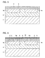
Fig.5 shows a cross sectional view of a step (4) of a manufacturing method of anitride semiconductor device 100. -
Fig.6 shows a cross sectional view of a step (5) of a manufacturing method of anitride semiconductor device 100. -
Fig.7 shows a cross sectional view of a step (6) of a manufacturing method of anitride semiconductor device 100. -
Fig.8 shows a cross sectional view of a step (7) of a manufacturing method of anitride semiconductor device 100. -
Fig.9 shows a cross sectional view of a step (8) of a manufacturing method of anitride semiconductor device 100. -
Fig.10 shows a cross sectional view of anitride semiconductor device 200 of a second embodiment. -
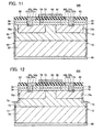
Fig.11 shows a cross sectional view of anitride semiconductor device 300 of a third embodiment. -
Fig.12 shows a cross sectional view of anitride semiconductor device 400 of a fourth embodiment. -
Fig.13 shows a cross sectional view of anitride semiconductor device 500 of prior art. - Preferred aspects of below embodiments will be listed.
- (Characterizing feature 1) The formula of a third nitride semiconductor layer is AlXGaYIn1-X-YN (where 0≤X≤1, 0≤Y≤1, 0≤1-X-Y≤1). In this case, a hetero junction surface can be formed between the third nitride semiconductor layer and a fourth nitride semiconductor layer.
- (Characterizing feature 2) A spacing of the region at which an etching damage is discontinuous is 1 µm or greater. In this case, flow of a leakage current at regions where the etching damage is discontinuous can be suppressed effectively.
- Embodiments are explained next with reference to accompanying drawings.
-
Fig. 1 is a cross-sectional diagram of part of anitride semiconductor device 100 according to the first embodiment. Thesemiconductor device 100 is an n-channel type vertical semiconductor device having a HEMT structure. Specifically, a drain electrode (back surface electrode) 18 is formed on a back surface, and a pair of source electrodes (front surface electrodes) 12a, 12b is formed on the front surface, such that currents flow in the vertical direction. Thenitride semiconductor device 100 comprises anitride semiconductor substrate 2. Thenitride semiconductor substrate 2 is formed of n+ type GaN. A firstnitride semiconductor layer 4 is stacked on the front surface of thenitride semiconductor substrate 2. The firstnitride semiconductor layer 4 is formed of n- type GaN. A pair of secondnitride semiconductor layers nitride semiconductor layer 4. The secondnitride semiconductor layers nitride semiconductor layer 4 is formed between the secondnitride semiconductor layers nitride semiconductor layers nitride semiconductor layer 9 is stacked on the front surface of the firstnitride semiconductor layer 4 and on the front surfaces of the secondnitride semiconductor layers nitride semiconductor layer 9 is formed of n- type GaN. The impurity concentration in the firstnitride semiconductor layer 4 and the thirdnitride semiconductor layer 9 is identical. A fourthnitride semiconductor layer 8 is stacked on the front surface of the thirdnitride semiconductor layer 9. The fourthnitride semiconductor layer 8 is formed of n- type AlGaN. The bandgap of the fourthnitride semiconductor layer 8 is greater than that of the thirdnitride semiconductor layer 9. The fourthnitride semiconductor layer 8 is in hetero junction with the thirdnitride semiconductor layer 9. - A pair of
openings nitride semiconductor layer 8 and at parts of the thirdnitride semiconductor layer 9, from the front surface of the fourthnitride semiconductor layer 8 and penetrating the thirdnitride semiconductor layer 9, reaching the front surfaces of the secondnitride semiconductor layers type source regions nitride semiconductor layers source regions nitride semiconductor layer 9 and the fourthnitride semiconductor layer 8, at positions facing the openings 11, such that hetero junction surfaces run across the interior of thesource regions source electrodes 12a, 12b is provided in therespective openings source electrodes 12a, 12b is in contact with parts of the front surfaces of the secondnitride semiconductor layers source regions source electrodes 12a, 12b are conductive with the thirdnitride semiconductor layer 9 and the fourthnitride semiconductor layer 8 via thesource regions nitride semiconductor layer 8 is covered by agate insulating film 10. A gate electrode (control electrode) 16 is provided on an area intervened by the pair ofsource electrodes 12a, 12b, on the front surface of thegate insulating film 10. The termination portion of thenitride semiconductor device 100 is in contact, for instance, with an element isolating section (not shown). For instance, an element isolating trench (not shown) is provided at the element isolating section, such that thenitride semiconductor device 100 is electrically isolated from other nitride semiconductor devices. - The operation of the
nitride semiconductor device 100 is explained next. Thenitride semiconductor device 100 is used with a voltage being applied across thesource electrodes 12a, 12b and thedrain electrode 18. If no positive voltage is applied to thegate electrode 16, no 2DEG forms at the hetero junction surface of the thirdnitride semiconductor layer 9 and the fourthnitride semiconductor layer 8. As a result, thenitride semiconductor device 100 is kept in an off state. When the positive voltage is applied to thegate electrode 16, a 2DEG forms at that hetero junction surface between the thirdnitride semiconductor layer 9 and the fourthnitride semiconductor layer 8, at a position between the pair ofsource regions nitride semiconductor device 100 is turned on. Thenitride semiconductor device 100 causes electrons to move by way of the 2DEG. Electron mobility is high, which enables highspeed operation. - Next, a method for manufacturing the
nitride semiconductor device 100 is explained. First, the n- type firstnitride semiconductor layer 4 is grown by MOCVD, using GaN as a material, on the front surface of the n+ typenitride semiconductor substrate 2 that has GaN as a material. The impurity concentration of thenitride semiconductor substrate 2 is 3×1018 cm-3. The introduced impurity is Si, and the thickness is 200 µm. The impurity concentration of the firstnitride semiconductor layer 4 is 3×1016 cm-3, the introduced impurity is Si, and the grown thickness is 6 µm. Next, as shown inFig. 2 , a p+ type secondnitride semiconductor layer 6, having GaN as a material, is formed by MOCVD on the front surface of the firstnitride semiconductor layer 4. The impurity concentration of the secondnitride semiconductor layer 6 is 1×1018cm-3, the introduced impurity is Mg, and the grown thickness is 0.5 µm. - Next, as shown in
Fig. 3 , firstsilicon oxide films 20 are formed at parts of a front surface of the secondnitride semiconductor layer 6. Next, dry etching is performed, using the firstsilicon oxide films 20 as the mask, from the front surface of the secondnitride semiconductor layer 6 to a front surface of the second nitride semiconductor layer 4 (down to a depth of 0.5 µm). As a result, the secondnitride semiconductor layer 6 is divided into the pair of secondnitride semiconductor layers front surface 4a of the firstnitride semiconductor layer 4 exposed by dry etching, to further form firstnitride semiconductor layer 4. Herein, the firstnitride semiconductor layer 4 is formed until the front surface of the firstnitride semiconductor layer 4 stands leveled at the same height as the front surface of the secondnitride semiconductor layers nitride semiconductor layer 4 is formed thereby. Next, as shown inFig. 4 , the firstsilicon oxide films 20 are removed, using an HF aqueous solution or the like. - Next, 100 nm of the n- type third
nitride semiconductor layer 9 are formed, by MOCVD, on the front surfaces of the firstnitride semiconductor layer 4 and the secondnitride semiconductor layers nitride semiconductor layer 9 are identical to those of the firstnitride semiconductor layer 4. Next, as shown inFig. 5 , the n- type fourthnitride semiconductor layer 8 having Al0.3Ga0.7N as a material is formed by MOCVD on a front surface of the thirdnitride semiconductor layer 9. The impurity concentration in the fourthnitride semiconductor layer 8 is 1×1016cm-3, and the grown thickness is 25 nm. Next, a second silicon oxide film (not shown) is formed on a front surface of the fourthnitride semiconductor layer 8. Next, parts of the second silicon oxide film are removed to expose the fourthnitride semiconductor layer 8 at areas where thesource regions nitride semiconductor layer 8. The implantation amount on N is 1×1016 cm-3, the acceleration voltage during implantation is 35 keV. The implantation amount on Si is 1×1015 cm-3, the acceleration voltage during implantation is 65 keV. Next, as shown inFig. 6 , the second silicon oxide film is removed, a thirdsilicon oxide film 24 is formed thereafter on the entire front surface, and annealing is performed. The annealing temperature is 1300°C and the annealing time is 5 minutes. The n+type source regions - Next the third
silicon oxide film 24 covering the fourthnitride semiconductor layer 8 on an outside of thesource regions Fig. 7 ,Al ions 22 are implanted through the front surface of the fourthnitride semiconductor layer 8. As a result of this implantation, theAl ions 22 reach down to the thirdnitride semiconductor layer 9, penetrating the fourthnitride semiconductor layer 8, at the portion not covered by the thirdsilicon oxide film 24. The resistivity of those portions within the thirdnitride semiconductor layer 9 that are implanted with Al ions, rises as a result. Next, the thirdsilicon oxide film 24 is removed, and a fourthsilicon oxide film 26 is formed on an entirety of the front surface. Next, parts of the fourthsilicon oxide film 26 are removed, to expose the fourthnitride semiconductor layer 8 at the areas where theopenings nitride semiconductor layer 8 that covers the termination portion. Next, as shown inFig. 8 , dry etching is performed, from a front surface of the exposed fourthnitride semiconductor layer 8, penetrating the thirdnitride semiconductor layer 9, and reaching the secondnitride semiconductor layers nitride semiconductor substrate 2, the firstnitride semiconductor layer 4 and the secondnitride semiconductor layers - Next, the fourth
silicon oxide film 26 is removed. Next, 50 nm of thegate insulating film 10 is formed by performing HTO (High-Temperature-Oxide)-CVD on the front surfaces of the fourthnitride semiconductor layer 8 and thesource regions Fig. 9 , parts of thegate insulating film 10 formed on the front surfaces of thesource regions source electrodes 12a, 12b is formed through vapor deposition, of Ti/Al films to a thickness of 10 nm/100 nm, respectively, at the front surface of the secondnitride semiconductor layers openings source regions drain electrode 18 is formed through vapor deposition of a Ti/Al film, to a thickness of 10 nm/100 nm, respectively, on the back surface of thenitride semiconductor substrate 2. Agate electrode 16 having Ni as a material is formed at a front surface of thegate insulating film 10, at an area positioned between the pair ofsource electrodes 12a, 12b above the fourthnitride semiconductor layer 8. As a result, the nitride semiconductor device 100 (Fig. 1 ) is completed. - In the method for manufacturing the
nitride semiconductor device 100, theetching damage 3 is formed at the termination portion of thenitride semiconductor substrate 2. In the part of the firstnitride semiconductor layer 4 at the termination portion of thenitride semiconductor device 100, anetching damage 5 whose n-type impurity concentration is higher than that at other portions of the firstnitride semiconductor layer 4 is formed.Etching damages nitride semiconductor layers nitride semiconductor layer 9. The etching damages 7a, 7b are imparted with n-type conductivity. As a result, theetching damages 7b formed directly below thefront surface electrodes 12a, 12b are surrounded by the secondnitride semiconductor layers etching damage 5 and the etching damages 7b are discontinuous. In thenitride semiconductor device 100, as a result, the current paths between thedrain electrode 18 and thesource electrodes 12a, 12b are discontinuous. The occurrence of the leakage current between thedrain electrode 18 and thesource electrodes 12a, 12b is thus suppressed. The spacing of the region at which etching damage is discontinuous (spacing between theetching damage 7a and theetching damage 7b) is 1 µm or greater. As a result, this allows effectively suppressing the flow of the leakage current at regions where the etching damage is discontinuous. -
Fig. 10 is a cross-sectional diagram of anitride semiconductor device 200 according to a second embodiment. InFig. 10 , those members resulting from adding 30 to the reference numerals ofFig. 1 are identical to the members explained inFig. 1 . In thenitride semiconductor device 200.source electrodes 42a. 42b are isolated from a thirdnitride semiconductor layer 39 and a fourthnitride semiconductor layer 38, on the termination portion side. In thenitride semiconductor device 200, as a result, the amount of metal material required for forming thesource electrodes nitride semiconductor device 100 of the first embodiment. -
Fig. 11 is a cross-sectional diagram of anitride semiconductor device 300 according to a third embodiment. InFig. 11 , those members resulting from adding 50 to the reference numerals ofFig. 1 are identical to the members explained inFig. 1 . In thenitride semiconductor device 300, a thirdnitride semiconductor layer 59 is provided continuously to the termination portion of thenitride semiconductor device 300. That is, the thirdnitride semiconductor layer 59 is provided on entire front surfaces of secondnitride semiconductor layers openings 61 a, 6 1b. - In the process of forming the openings 61a, 61b (process corresponding to
Fig. 8 of the first embodiment) during the method for manufacturing thenitride semiconductor device 300, etching is performed only at the areas where the openings 61 a, 61 b are to be formed. As a result, etching damage is formed only at the termination portion of the nitride semiconductor substrate 52, the termination portion of the firstnitride semiconductor layer 54, and the front surfaces of the secondnitride semiconductor layers etching damage 55 are discontinuous. In thenitride semiconductor device 300, no etching damage is formed at the front surfaces of the secondnitride semiconductor layers nitride semiconductor device 100 of the first embodiment. The occurrence of leakage current between adrain electrode 68 andsource electrodes -
Fig. 12 is a cross-sectional diagram of anitride semiconductor device 400 according to a fourth embodiment. InFig. 11 those members resulting from adding 70 to the reference numerals ofFig. 1 are identical to the members explained inFig. 1 . Thenitride semiconductor device 400 has the structure of thenitride semiconductor device 300 of the third embodiment but herein the firstnitride semiconductor layer 54 that covers the side faces of the secondnitride semiconductor layers nitride semiconductor layers nitride semiconductor device 400, thus, the side faces of secondnitride semiconductor layers 76a, 76b are exposed. Therefore, the region at which etching damage is formed in the firstnitride semiconductor layer 74 is reduced. Herein,etching damage 75 that forms in the firstnitride semiconductor layer 74 is n+ type, andetching damage 77b that is formed in the secondnitride semiconductor layers 76a, 76b is n- type. Therefore, theetching damage 75 that is formed in the firstnitride semiconductor layer 74 has lower carrier resistance than the etching damages 77b that are formed in the secondnitride semiconductor layers 76a, 76b. That is, the leakage current flows more readily in theetching damage 75 than in the etching damages 77b. In thenitride semiconductor device 400, the leakage current that occurs between adrain electrode 88 andsource electrodes etching damage 75 that is formed in the firstnitride semiconductor layer 74. - Specific embodiment of the present invention is described above, but this merely illustrates some representative possibilities for utilizing the invention and does not restrict the claims thereof. The subject matter set forth in the claims includes variations and modifications of the specific examples set forth above. The technical elements disclosed in the specification or the drawings may be utilized separately or in all types of combinations, and are not limited to the combinations set forth in the claims at the time of filing of the application. Furthermore, the subject matter disclosed herein may be utilized to simultaneously achieve a plurality of objects or to only achieve one object.
-
- 2, 32, 52, 72, 102: nitride semiconductor substrate
- 3, 33, 53, 73: etching damage (formed in a nitride semiconductor substrate)
- 4, 34, 54, 74, 104: first nitride semiconductor layer
- 5, 35, 55, 75: etching damage (formed in a first semiconductor layer)
- 6a, 6b, 36a, 36b, 56a, 56b, 76a, 76b, 106a, 106b: second nitride semiconductor layer
- 7a, 7b, 37a, 37b, 57a, 57b, 77a, 77b: etching damage (formed in a second semiconductor layer)
- 8, 38, 58, 78, 108: fourth nitride semiconductor layer
- 9, 39, 59, 79, 109: third nitride semiconductor layer
- 10,40, 60, 80, 110: gate insulator film
- 11a, 11b, 41a, 41b, 61a, 61 b, 81a, 81b: opening
- 12a, 12b, 42a, 42b, 62a, 62b, 82a, 82b, 112a, 112b: source electrode
- 14a, 14b, 44a, 44b, 64a, 64b, 84a, 84b, 114a, 114b: source region
- 16, 46, 66, 86, 116: gate electrode
- 18, 48, 68, 88, 118: drain electrode
- 22: Aluminum ion
- 24: third silicon oxide film
- 26: fourth silicon oxide film
- 100, 200, 300, 400, 500: nitride semiconductor device
- 103, 105, 107: etching damaged region
Claims (8)
- A nitride semiconductor device, comprising:a first nitride semiconductor layer of n-type;a second nitride semiconductor layer of p-type formed on a part of a front surface of the first nitride semiconductor layer;a third nitride semiconductor layer of n-type formed on the front surface of the first nitride semiconductor layer and a front surface of the second nitride semiconductor layer; anda front surface electrode formed on a part of the front surface of the second nitride semiconductor layer;wherein an opening is formed in the third nitride semiconductor layer at a position isolated from a peripheral edge of the third nitride semiconductor layer, penetrating the third nitride semiconductor layer and reaching the front surface of the second nitride semiconductor layer, andthe front surface electrode is formed inside the opening.
- The nitride semiconductor device as in claim 1, further comprising:a fourth nitride semiconductor layer of n-type in hetero junction with a front surface of the third nitride semiconductor layer.
- The nitride semiconductor device as in claim 1 or 2, wherein
the front surface electrode is isolated from the third nitride semiconductor layer formed between a termination portion of the nitride semiconductor device and the opening. - The nitride semiconductor device as in any one of claims 1 to 3, wherein
the third nitride semiconductor layer is formed to a termination portion of the nitride semiconductor device. - The nitride semiconductor device as in any one of claims 1 to 4. wherein
a termination portion of the second nitride semiconductor layer is exposed. - A nitride semiconductor device, comprising:a first nitride semiconductor layer of n-type;a second nitride semiconductor layer of p-type formed on a part of a front surface of the first nitride semiconductor layer;a third nitride semiconductor layer of n-type formed on the front surface of the first nitride semiconductor layer and a front surface of the second nitride semiconductor layer; anda front surface electrode formed on a part of the front surface of the second nitride semiconductor layer;wherein an etching damage is formed at a portion making contact with the front surface electrode within a region facing the front surface of the second nitride semiconductor layer, andthe etching damage is surrounded by the second nitride semiconductor layer not having the etching damage.
- A method of manufacturing the nitride semiconductor device as in any one of claims 1 to 6, comprising:a third nitride semiconductor layer forming step for forming the third nitride semiconductor layer on the front surface of the second nitride semiconductor layer;an opening forming step for forming the opening by etching a part of the third nitride semiconductor layer from a front surface of the third nitride semiconductor layer, penetrating the third nitride semiconductor layer and reaching the second nitride semiconductor layer, anda front surface electrode forming step for forming the front surface electrode on the front surface of the second nitride semiconductor layer exposed inside the opening.
- The method of claim 7, further comprising:an ion doping step for doping ionized nitride, aluminum, carbon, or magnesium to a portion of the third nitride semiconductor layer between a termination portion of the nitride semiconductor device and the opening.
Applications Claiming Priority (1)
| Application Number | Priority Date | Filing Date | Title |
|---|---|---|---|
| PCT/JP2009/053834 WO2010100709A1 (en) | 2009-03-02 | 2009-03-02 | Nitride semiconductor device and method for manufacturing the same |
Publications (1)
| Publication Number | Publication Date |
|---|---|
| EP2405467A1 true EP2405467A1 (en) | 2012-01-11 |
Family
ID=42709287
Family Applications (1)
| Application Number | Title | Priority Date | Filing Date |
|---|---|---|---|
| EP09841075A Withdrawn EP2405467A1 (en) | 2009-03-02 | 2009-03-02 | Nitride semiconductor device and method for manufacturing the same |
Country Status (5)
| Country | Link |
|---|---|
| US (1) | US20110316049A1 (en) |
| EP (1) | EP2405467A1 (en) |
| JP (1) | JPWO2010100709A1 (en) |
| CN (1) | CN102341898A (en) |
| WO (1) | WO2010100709A1 (en) |
Families Citing this family (9)
| Publication number | Priority date | Publication date | Assignee | Title |
|---|---|---|---|---|
| JP5569321B2 (en) * | 2010-10-07 | 2014-08-13 | 住友電気工業株式会社 | Semiconductor device and manufacturing method thereof |
| JP2012156250A (en) * | 2011-01-25 | 2012-08-16 | Toyota Motor Corp | Semiconductor device including p-type group iii nitride semiconductor layer, and method for manufacturing the same |
| US8470652B1 (en) * | 2011-05-11 | 2013-06-25 | Hrl Laboratories, Llc | Monolithic integration of group III nitride enhancement layers |
| JP5841417B2 (en) * | 2011-11-30 | 2016-01-13 | 株式会社日立製作所 | Nitride semiconductor diode |
| JP6245791B2 (en) * | 2012-03-27 | 2017-12-13 | 日亜化学工業株式会社 | Vertical nitride semiconductor device and manufacturing method thereof |
| US9583608B2 (en) * | 2012-08-03 | 2017-02-28 | Panasonic Intellectual Property Management Co., Ltd. | Nitride semiconductor device and method for manufacturing nitride semiconductor device |
| CN107731889A (en) * | 2016-08-12 | 2018-02-23 | 比亚迪股份有限公司 | High electron mobility semiconductor device and preparation method thereof |
| US10204778B2 (en) * | 2016-12-28 | 2019-02-12 | QROMIS, Inc. | Method and system for vertical power devices |
| DE102019212645A1 (en) * | 2019-08-23 | 2021-02-25 | Robert Bosch Gmbh | VERTICAL FIELD EFFECT TRANSISTOR AND METHOD OF MANUFACTURING THE SAME |
Family Cites Families (6)
| Publication number | Priority date | Publication date | Assignee | Title |
|---|---|---|---|---|
| JP2002314097A (en) * | 2001-04-16 | 2002-10-25 | Auto Network Gijutsu Kenkyusho:Kk | Junction type field effect transistor |
| DE10213534B4 (en) * | 2002-03-26 | 2007-06-21 | Siced Electronics Development Gmbh & Co. Kg | Semiconductor structure with switching element and edge element |
| JP4645034B2 (en) * | 2003-02-06 | 2011-03-09 | 株式会社豊田中央研究所 | Semiconductor device having group III nitride semiconductor |
| JP5087818B2 (en) * | 2005-03-25 | 2012-12-05 | 日亜化学工業株式会社 | Field effect transistor |
| JP2008078332A (en) * | 2006-09-20 | 2008-04-03 | Toyota Central R&D Labs Inc | Method for manufacturing p-type group III nitride semiconductor and method for manufacturing electrode for p-type group III nitride semiconductor |
| JP5122165B2 (en) * | 2007-03-20 | 2013-01-16 | 株式会社豊田中央研究所 | Semiconductor device and manufacturing method thereof |
-
2009
- 2009-03-02 WO PCT/JP2009/053834 patent/WO2010100709A1/en not_active Ceased
- 2009-03-02 CN CN2009801577600A patent/CN102341898A/en active Pending
- 2009-03-02 EP EP09841075A patent/EP2405467A1/en not_active Withdrawn
- 2009-03-02 US US13/254,638 patent/US20110316049A1/en not_active Abandoned
- 2009-03-02 JP JP2011502517A patent/JPWO2010100709A1/en not_active Withdrawn
Non-Patent Citations (1)
| Title |
|---|
| See references of WO2010100709A1 * |
Also Published As
| Publication number | Publication date |
|---|---|
| CN102341898A (en) | 2012-02-01 |
| US20110316049A1 (en) | 2011-12-29 |
| WO2010100709A1 (en) | 2010-09-10 |
| JPWO2010100709A1 (en) | 2012-09-06 |
Similar Documents
| Publication | Publication Date | Title |
|---|---|---|
| EP2405467A1 (en) | Nitride semiconductor device and method for manufacturing the same | |
| US9673289B2 (en) | Dual oxide trench gate power MOSFET using oxide filled trench | |
| CN109728092B (en) | Fully-coated grid structure and manufacturing method thereof | |
| US20190221666A1 (en) | Semiconductor device and method of manufacturing the same | |
| US20100144109A1 (en) | Transistor in a semiconductor substrate having high-concentration source and drain region formed at the bottom of a trench adjacent to the gate electrode | |
| US8846469B2 (en) | Fabrication method of trenched power semiconductor device with source trench | |
| US7605038B2 (en) | Semiconductor device and manufacturing method thereof | |
| US8940607B2 (en) | Manufacturing method of trench type power transistor device with super junction | |
| US9484437B2 (en) | Lateral double diffused metal oxide semiconductor device and manufacturing method thereof | |
| CN108336141A (en) | Semiconductor device and its manufacturing method | |
| US20220165880A1 (en) | High voltage device and manufacturing method thereof | |
| US9640672B2 (en) | Diode device and method for manufacturing the same | |
| US10910493B2 (en) | Semiconductor device and method of manufacturing the same | |
| US7948031B2 (en) | Semiconductor device and method of fabricating semiconductor device | |
| CN216671642U (en) | Integrated circuit with a plurality of transistors | |
| US9024409B2 (en) | Semiconductor device and method for forming the same | |
| JP2016058626A (en) | Semiconductor device and manufacturing method thereof | |
| CN113597661A (en) | Semiconductor device and method for manufacturing semiconductor device | |
| KR20170109422A (en) | Semiconductor device and method for manufacturing the same | |
| CN114068670B (en) | Semiconductor structure and forming method thereof | |
| WO2015006131A1 (en) | Method to fabricate self-aligned isolation in gallium nitride devices and integrated circuits | |
| JP6243748B2 (en) | Semiconductor device and manufacturing method thereof | |
| JP5037103B2 (en) | Silicon carbide semiconductor device | |
| US10497806B2 (en) | Metal oxide semiconductor device having recess and manufacturing method thereof | |
| US20160218014A1 (en) | Semiconductor device and method of manufacturing the same |
Legal Events
| Date | Code | Title | Description |
|---|---|---|---|
| PUAI | Public reference made under article 153(3) epc to a published international application that has entered the european phase |
Free format text: ORIGINAL CODE: 0009012 |
|
| 17P | Request for examination filed |
Effective date: 20110929 |
|
| AK | Designated contracting states |
Kind code of ref document: A1 Designated state(s): AT BE BG CH CY CZ DE DK EE ES FI FR GB GR HR HU IE IS IT LI LT LU LV MC MK MT NL NO PL PT RO SE SI SK TR |
|
| DAX | Request for extension of the european patent (deleted) | ||
| RAP1 | Party data changed (applicant data changed or rights of an application transferred) |
Owner name: TOYOTA JIDOSHA KABUSHIKI KAISHA |
|
| STAA | Information on the status of an ep patent application or granted ep patent |
Free format text: STATUS: THE APPLICATION HAS BEEN WITHDRAWN |
|
| 18W | Application withdrawn |
Effective date: 20130614 |