EP2405438A1 - Method for writing in a MRAM-based memory device with reduced power consumption - Google Patents
Method for writing in a MRAM-based memory device with reduced power consumption Download PDFInfo
- Publication number
- EP2405438A1 EP2405438A1 EP10168737A EP10168737A EP2405438A1 EP 2405438 A1 EP2405438 A1 EP 2405438A1 EP 10168737 A EP10168737 A EP 10168737A EP 10168737 A EP10168737 A EP 10168737A EP 2405438 A1 EP2405438 A1 EP 2405438A1
- Authority
- EP
- European Patent Office
- Prior art keywords
- voltage
- tunnel junction
- magnetic tunnel
- word line
- memory device
- Prior art date
- Legal status (The legal status is an assumption and is not a legal conclusion. Google has not performed a legal analysis and makes no representation as to the accuracy of the status listed.)
- Granted
Links
- 238000000034 method Methods 0.000 title claims abstract description 22
- 238000010438 heat treatment Methods 0.000 claims abstract description 30
- 230000005415 magnetization Effects 0.000 description 10
- 230000008014 freezing Effects 0.000 description 3
- 238000007710 freezing Methods 0.000 description 3
- 230000011218 segmentation Effects 0.000 description 2
- 230000003247 decreasing effect Effects 0.000 description 1
- 230000000593 degrading effect Effects 0.000 description 1
- 230000005684 electric field Effects 0.000 description 1
- 230000003116 impacting effect Effects 0.000 description 1
- 230000010354 integration Effects 0.000 description 1
Images

Classifications
-
- G—PHYSICS
- G11—INFORMATION STORAGE
- G11C—STATIC STORES
- G11C8/00—Arrangements for selecting an address in a digital store
- G11C8/08—Word line control circuits, e.g. drivers, boosters, pull-up circuits, pull-down circuits, precharging circuits, for word lines
-
- G—PHYSICS
- G11—INFORMATION STORAGE
- G11C—STATIC STORES
- G11C11/00—Digital stores characterised by the use of particular electric or magnetic storage elements; Storage elements therefor
- G11C11/02—Digital stores characterised by the use of particular electric or magnetic storage elements; Storage elements therefor using magnetic elements
- G11C11/16—Digital stores characterised by the use of particular electric or magnetic storage elements; Storage elements therefor using magnetic elements using elements in which the storage effect is based on magnetic spin effect
- G11C11/165—Auxiliary circuits
- G11C11/1675—Writing or programming circuits or methods
-
- G—PHYSICS
- G11—INFORMATION STORAGE
- G11C—STATIC STORES
- G11C11/00—Digital stores characterised by the use of particular electric or magnetic storage elements; Storage elements therefor
- G11C11/02—Digital stores characterised by the use of particular electric or magnetic storage elements; Storage elements therefor using magnetic elements
- G11C11/16—Digital stores characterised by the use of particular electric or magnetic storage elements; Storage elements therefor using magnetic elements using elements in which the storage effect is based on magnetic spin effect
- G11C11/165—Auxiliary circuits
- G11C11/1673—Reading or sensing circuits or methods
Definitions
- the present disclosure relates to a method of writing in a memory device comprising a plurality of magnetoresistive random access memory (MRAM) cells allowing for reduced power consumption.
- MRAM magnetoresistive random access memory
- FIG. 1 A conventional memory device based on magnetic random access memory (MRAM) cells is shown schematically in Fig. 1 .
- the memory device 10 typically includes an array of word lines WL and bit lines BL that intersects to form an array.
- a MRAM cell 1 is coupled at each intersection of the word lines WL and bit lines BL.
- Each MRAM cell 1 comprises a magnetic tunnel junction 2, represented by a resistance, electrically coupled at one end to a select CMOS transistor 3.
- the magnetic tunnel junction 2 is typically formed to form an insulating layer in-between a reference layer and a storage layer (these element are not shown in Fig.1 ).
- the word lines WL connect the MRAM cells 1 along a row via the gate of their respective transistors 3, while the bit lines BL connect the MRAM cells 1 along a column via the other end of their respective magnetic tunnel junction 2.
- One of the MRAM cells 1, located at a corresponding intersection of one of the bit and word lines BL, WL, can be selected by providing the corresponding bit and word lines with a predetermined bias voltage value.
- a selection circuitry 4 allows for selecting the bit and word lines BL, WL being supplied with the bias voltage.
- thermally assisted switching (TAS) writing operation of the selected MRAM cell data is written by applying a single heating current pulse I heat through the magnetic tunnel junction 2 in order to heat it above a predetermined high threshold temperature, while a magnetic field or a spin polarized current is applied to switch the magnetization of the storage layer.
- the MRAM cell 1 is then cooled down by switching off the heating current pulse I heat , thereby freezing the magnetization of the storage layer in the written direction.
- the data is then read by measuring the resistance magnetic tunnel junction, or magnetoresistance, by applying a sense voltage across the magnetic tunnel junction, at ambient temperature, or by passing a sense current through the magnetic tunnel junction and reading the resultant voltage.
- One of the major drawbacks of this writing procedure is the necessary heating current I heat to raise the temperature of the storage layer above its threshold temperature. Indeed, during the writing operation, the heating current is controlled by the bias voltage applied to both word and bit lines WL, BL.
- the magnitude of the heating current I heat required to heat the magnetic tunnel junction 2 above the predetermined high threshold temperature imposes a constraint on the conductivity of the select transistor 3, depending on the size of the magnetic tunnel junction 2 in series with the transistor 3. For example, in order to reach a threshold temperature of 150°C in the magnetic tunnel junction 2 having a surface area of 3.14 ⁇ 10 -2 ⁇ m 2 , the heating current I heat must have a value of about 200 ⁇ A, when using a low size select transistor (for example of 0.13 ⁇ m).
- I heat A * Pd RA
- A the surface area of the magnetic tunnel junction 2
- P d the current power density in Watts cm -2
- RA the resistance-area product of the magnetic tunnel junction (insulating layer) in ⁇ cm 2 .
- the gate length and the oxide film thickness of the select transistor 3 are reduced. Therefore, a low memory array voltage, or core voltage, is used to power-up the MRAM cell 1, such as to reduce the power consumption and to improve the reliability of the select transistor 3. Indeed, using a high core voltage would produce a high channel electric field, possibly reaching a voltage-resistant limit of the select transistor oxide film, thus degrading the reliability of the select transistor 3.
- the core voltage has a value of 1.2 volts
- a voltage of 1.2 volts is applied to the world line WL and the bit line BL
- the resulting heating current I heat flowing through the magnetic tunnel junction 2 has a value of 130 ⁇ A. This is insufficient to reach the high threshold temperature of 150°C, and the cell 1 cannot be written.
- the present application discloses a method of writing in a memory device comprising a plurality of magnetoresistive random access memory (MRAM) cells which overcome at least some limitations of the prior art.
- MRAM magnetoresistive random access memory
- a method of writing in a memory device comprising a plurality of MRAM cells arranged in rows and columns, each MRAM cell including a magnetic tunnel junction having a resistance that can be varied during a write operation when the magnetic tunnel junction is heated at a high threshold temperature, and a select transistor electrically coupled to the magnetic tunnel junction; a plurality of word lines connecting MRAM cells along a row; and a plurality of bit lines connecting MRAM cells along a column; can comprise, during the write operation, supplying a bit line voltage to one of the bit lines and a word line voltage to one of the word lines for passing a heating current through the magnetic tunnel junction of a selected MRAM cell; characterized in that said word line voltage is a word line overdrive voltage being higher than the core operating voltage of the MRAM cells such that the heating current has a magnitude that is high enough for heating the magnetic tunnel junction at the predetermined high threshold temperature.
- the word line overdrive voltage can be a voltage pulse with a pulse duration being equal to or smaller than about 15 ns.
- the word line overdrive voltage can be generated by a charge pump or by a regulable external voltage provided by an input-output port.
- the memory device can further comprise a sense amplifier circuitry, and wherein the pulse duration of the word line overdrive voltage can be controlled by the sense amplifier circuitry.
- the select transistor can be a high power transistor having a low threshold voltage.
- the memory device can further comprise a plurality of source lines connecting MRAM cells along a row, via the drain of their respective select transistor, and wherein the method can further comprise supplying a source line overdrive voltage to the source line.
- the source line overdrive voltage can have a value substantially equal to the threshold voltage of the select transistor.
- the method can further comprise a read operation including measuring the resistance of the magnetic tunnel junction, and supplying the source line overdrive voltage to the source line.
- the disclosed method allows for passing the heating current with a sufficient magnitude such that the magnetic tunnel junction can be heated at a temperature that is high enough to reach a high threshold temperature appropriate for varying its resistance, without increasing the size of the transistors. Indeed, the disclosed method allows for collecting a high heating current density on the transistor drain without increasing the transistor size. The disclosed method allows for using low size transistors and therefore, the memory device can have a high-density and can be written with low power consumption.
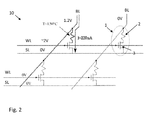
- Fig. 2 represents schematically a memory device 10 according to a preferred embodiment.
- the memory device 10 comprises a plurality of magnetoresistive random access memory (MRAM) cells 1 arranged in rows and columns. Four of such MRAM cells 1 are shown in Fig. 2 .
- Each MRAM cell 1 comprises a magnetic tunnel junction 2, represented by a resistance in Fig. 1 , electrically coupled at one end to a select CMOS transistor 3.
- the magnetic tunnel junction 2 can be formed of a reference layer having a fixed magnetization, a storage layer having a magnetization direction that can be switched from a first stable direction to a second stable direction upon writing of the cell, and an insulating layer between the storage layer and the sense layer.
- the MRAM cell 1 can be written by using a thermally-assisted switching (TAS) write operation.
- TAS thermally-assisted switching
- Such TAS write operation requires heating the magnetic tunnel junction 2 at a high threshold temperature in order to switch the magnetization of the storage layer and then cool the magnetic tunnel junction 2 at a low threshold temperature, below the high threshold temperature, in order to freeze the magnetization of the storage layer in the written state.
- the magnetic tunnel junction 2 has a resistance which value can be changed during the TAS write operation 2 when heating the magnetic tunnel junction 2 at the high threshold temperature.
- the memory device 10 comprises a plurality of bit lines BL and word lines WL forming an angle, preferably orthogonal, with the bit lines BL.
- the bit lines BL connect the MRAM cells 1 along a column, via the other end of their magnetic tunnel junction 2, and the word lines WL connect the MRAM cells 1 along a row via the gate of their select transistor 3.
- the memory device 10 further comprises a plurality of source lines SL arranged substantially orthogonal with the bit lines BL, each source line SL connecting the MRAM cells 1 along a row, via the drain of their respective select transistor 3.
- data is written in one of the MRAM cells 1 by supplying a bit line voltage V BL to one of the bit lines BL, and supplying a word line voltage V WL to one of the word lines WL.
- the MRAM cell 1 being written, or the selected MRAM cell 1 is the cell 1 addressed by the bit and word lines BL, WL being supplied by the respective bit line and word line voltages V BL and V WL .
- the value of the voltages V BL and V WL usually correspond to a maximum supply voltage V DD , or core voltage that is determined by the specifications of the select transistor 3, and enable passing a heating current I heat through the magnetic tunnel junction 1 of the selected MRAM cell 1.
- the select transistor 3 has a size of 0.13 ⁇ m
- the core voltage, or gate-to-source voltage V GS of the select transistor 3 has a value typically of1.2 V.
- the word line voltage V WL supplied to one of the word lines WL corresponds to a word line overdrive voltage V WLo that is higher than a core operating voltage of the MRAM cell 1, during a writing period of the write operation.
- the value of the word line overdrive voltage V WLo is determined such that the select transistor 3 drives the heating current I heat having a magnitude that is high enough for heating the magnetic tunnel junction 2 at the high threshold temperature. More particularly, the value of the word line overdrive voltage V WLo is determined taking into account the size and density of the MRAM cells 1 and the foundry design rules for oxide stress of the magnetic tunnel junction 2 such as to avoid impacting on the reliability of the memory device 10.
- the word line overdrive voltage V WLo can be generated by an internal charge pump (not shown), or from a regulable external voltage V DD being higher than the core operating voltage and provided by an input-output port IO (also not shown).
- the word line overdrive voltage V WLo having a magnitude of 2 V allows passing the heating current I heat with a magnitude of 220 ⁇ A in the case the magnetic tunnel junction 2 of the MRAM cell 1 has a diameter of 100 nm and a resistance-area product (RA) of about 30 ⁇ cm 2 .
- the magnetic tunnel junction 2 Once the magnetic tunnel junction 2 has reached the high threshold temperature, its resistance can be varied, for example, by applying a magnetic field to the magnetic tunnel junction 2 or by passing a spin polarized current through the magnetic tunnel junction 2.
- the magnetic tunnel junction resistance can be varied by adjusting the magnetization direction of the storage layer.
- a high resistance is measured when the magnetization direction of the storage layer is substantially opposed to the one of the reference layer, and a low resistance is measure when the respective magnetizations of the storage and reference layers are oriented substantially in the same direction.
- the selected MRAM cell 1 is then cooled down by switching off the heating current pulse I heat , thereby freezing the magnetic tunnel junction resistance in its written value, for example, by freezing the magnetization of the storage layer in the written direction.
- the word line overdrive voltage V WLo is a voltage pulse which duration, or width, can be controlled such as to avoid possible stress on the gate oxide of the select transistor 3. This can be especially important in the case the MRAM cell is manually written by a user.
- the control of the voltage pulse can be performed, for example, using internal timers (not shown).
- the word line overdrive voltage V WLo has a voltage pulse duration typically around 15 ns or smaller.
- the memory device 10 can further comprise a sense amplifier circuitry (not shown) used to latch the correct state of the MRAM cell 1, and hold the input-output IO in this state until a new address is selected, corresponding to selecting another MRAM cell 1.
- a sense amplifier circuitry (not shown) used to latch the correct state of the MRAM cell 1, and hold the input-output IO in this state until a new address is selected, corresponding to selecting another MRAM cell 1.
- the control of the word line overdrive voltage pulse V WLo must be timed with the sense amplifier circuitry, or the word line overdrive voltage V WLo pulse duration is controlled by the sense amplifier circuitry.
- the select transistor 3 is a high power HP transistor having a low threshold voltage V th .
- HP transistor can drive more current than standard CMOS transistors for a given gate voltage.
- a drawback of HP transistors is their large OFF-state current I off when the gate-to-source voltage V GS is zero.
- High I off leakage of the bit line BL can limit the number of MRAM cells 1 which can be connected to one segment of bit line BL, since this I off leakage can possibly degrade the sense amplifier margins to unacceptable levels. Typically higher sensing margin is obtained for a smaller leakage current.
- Using several small segments of bit lines BL is not advantageous since this requires using several bit line segmentation transistors (not shown) that are typically quite large and costly to implement.
- the OFF-state current I off leakage is reduced by using a negative gate driving scheme. Reducing the I off leakage thus allows connecting more MRAM cells per segment of bit line BL and, consequently, a denser memory device 10 and lower costs, since less segmentation transistors are needed.
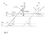
- Fig. 3 represents yet another embodiment of the memory device 10 where the select transistors 3 can be HP transistors.
- a source line overdrive voltage V SLo is supplied to the source line SL in order to reduce the leakage current I off .
- the source line overdrive voltage V SLo can have a value equal or close to the value of the threshold voltage V th of the select transistor 3.
- data written in the selected MRAM cell 1 is read by measuring the magnetic tunnel junction resistance of the cell 1. This can be performed by applying a sense voltage (not shown) across the magnetic tunnel junction 2, at ambient temperature, or by passing a sense current (also not shown) through the magnetic tunnel junction 2 and reading the resultant voltage.
- the power consumption of the memory device 10 can be minimized by supplying the same source line overdrive voltage V SLo to the source lines SL during the read operation as during the write operation.
- the gate of the select transistors 3 can then be over-driven by applying the word line overdrive voltage V WLo to the world lines WL, such that the heating current I heat flowing through the magnetic tunnel junction 2 has a magnitude high enough for heating the magnetic tunnel junction 2 above the predetermined high threshold temperature.
- the above method allows for using low size transistors (3) and therefore, the memory device can have a high-density and can be written with low power consumption.
Landscapes
- Engineering & Computer Science (AREA)
- Computer Hardware Design (AREA)
- Microelectronics & Electronic Packaging (AREA)
- Mram Or Spin Memory Techniques (AREA)
- Hall/Mr Elements (AREA)
Abstract
Description
- The present disclosure relates to a method of writing in a memory device comprising a plurality of magnetoresistive random access memory (MRAM) cells allowing for reduced power consumption.
- A conventional memory device based on magnetic random access memory (MRAM) cells is shown schematically in
Fig. 1 . Thememory device 10 typically includes an array of word lines WL and bit lines BL that intersects to form an array. AMRAM cell 1 is coupled at each intersection of the word lines WL and bit lines BL. EachMRAM cell 1 comprises amagnetic tunnel junction 2, represented by a resistance, electrically coupled at one end to aselect CMOS transistor 3. Themagnetic tunnel junction 2 is typically formed to form an insulating layer in-between a reference layer and a storage layer (these element are not shown inFig.1 ). The word lines WL connect theMRAM cells 1 along a row via the gate of theirrespective transistors 3, while the bit lines BL connect theMRAM cells 1 along a column via the other end of their respectivemagnetic tunnel junction 2. - One of the
MRAM cells 1, located at a corresponding intersection of one of the bit and word lines BL, WL, can be selected by providing the corresponding bit and word lines with a predetermined bias voltage value. In the example ofFig.1 , aselection circuitry 4 allows for selecting the bit and word lines BL, WL being supplied with the bias voltage. - During a so-called thermally assisted switching (TAS) writing operation of the selected
MRAM cell 1, data is written by applying a single heating current pulse Iheat through themagnetic tunnel junction 2 in order to heat it above a predetermined high threshold temperature, while a magnetic field or a spin polarized current is applied to switch the magnetization of the storage layer. TheMRAM cell 1 is then cooled down by switching off the heating current pulse Iheat, thereby freezing the magnetization of the storage layer in the written direction. - The data is then read by measuring the resistance magnetic tunnel junction, or magnetoresistance, by applying a sense voltage across the magnetic tunnel junction, at ambient temperature, or by passing a sense current through the magnetic tunnel junction and reading the resultant voltage.
- One of the major drawbacks of this writing procedure is the necessary heating current Iheat to raise the temperature of the storage layer above its threshold temperature. Indeed, during the writing operation, the heating current is controlled by the bias voltage applied to both word and bit lines WL, BL. The magnitude of the heating current Iheat required to heat the
magnetic tunnel junction 2 above the predetermined high threshold temperature imposes a constraint on the conductivity of theselect transistor 3, depending on the size of themagnetic tunnel junction 2 in series with thetransistor 3. For example, in order to reach a threshold temperature of 150°C in themagnetic tunnel junction 2 having a surface area of 3.14·10-2 µm2, the heating current Iheat must have a value of about 200 µA, when using a low size select transistor (for example of 0.13 µm). Here, the heating current Iheat is given by Equation 1:
where A is the surface area of themagnetic tunnel junction 2, Pd the current power density in Watts cm-2, and RA the resistance-area product of the magnetic tunnel junction (insulating layer) in Ω cm2. - Since the size of the
MRAM cell 1 is generally decreased due to increasing level of integration and scale down, the gate length and the oxide film thickness of theselect transistor 3 are reduced. Therefore, a low memory array voltage, or core voltage, is used to power-up theMRAM cell 1, such as to reduce the power consumption and to improve the reliability of theselect transistor 3. Indeed, using a high core voltage would produce a high channel electric field, possibly reaching a voltage-resistant limit of the select transistor oxide film, thus degrading the reliability of theselect transistor 3. - It is therefore difficult to generate a value of the heating current that is high enough in
most MRAM cells 1 by using the low core voltage. For example, in the case the core voltage has a value of 1.2 volts, and a voltage of 1.2 volts is applied to the world line WL and the bit line BL, the resulting heating current Iheat flowing through themagnetic tunnel junction 2 has a value of 130 µA. This is insufficient to reach the high threshold temperature of 150°C, and thecell 1 cannot be written. - The present application discloses a method of writing in a memory device comprising a plurality of magnetoresistive random access memory (MRAM) cells which overcome at least some limitations of the prior art.
- According to the embodiments, a method of writing in a memory device comprising a plurality of MRAM cells arranged in rows and columns, each MRAM cell including a magnetic tunnel junction having a resistance that can be varied during a write operation when the magnetic tunnel junction is heated at a high threshold temperature, and a select transistor electrically coupled to the magnetic tunnel junction; a plurality of word lines connecting MRAM cells along a row; and a plurality of bit lines connecting MRAM cells along a column; can comprise, during the write operation, supplying a bit line voltage to one of the bit lines and a word line voltage to one of the word lines for passing a heating current through the magnetic tunnel junction of a selected MRAM cell; characterized in that said word line voltage is a word line overdrive voltage being higher than the core operating voltage of the MRAM cells such that the heating current has a magnitude that is high enough for heating the magnetic tunnel junction at the predetermined high threshold temperature.
- In an embodiment, the word line overdrive voltage can be a voltage pulse with a pulse duration being equal to or smaller than about 15 ns.
- In another embodiment, the word line overdrive voltage can be generated by a charge pump or by a regulable external voltage provided by an input-output port.
- In yet an embodiment, the memory device can further comprise a sense amplifier circuitry, and wherein the pulse duration of the word line overdrive voltage can be controlled by the sense amplifier circuitry.
- In yet an embodiment, the select transistor can be a high power transistor having a low threshold voltage.
- In yet an embodiment, the memory device can further comprise a plurality of source lines connecting MRAM cells along a row, via the drain of their respective select transistor, and wherein the method can further comprise supplying a source line overdrive voltage to the source line.
- In yet an embodiment, the source line overdrive voltage can have a value substantially equal to the threshold voltage of the select transistor.
- In yet an embodiment, the method can further comprise a read operation including measuring the resistance of the magnetic tunnel junction, and supplying the source line overdrive voltage to the source line.
- The disclosed method allows for passing the heating current with a sufficient magnitude such that the magnetic tunnel junction can be heated at a temperature that is high enough to reach a high threshold temperature appropriate for varying its resistance, without increasing the size of the transistors. Indeed, the disclosed method allows for collecting a high heating current density on the transistor drain without increasing the transistor size. The disclosed method allows for using low size transistors and therefore, the memory device can have a high-density and can be written with low power consumption.
- Preferred embodiments will be better understood with the aid of the description of an embodiment given by way of example and illustrated by the figures, in which:
-
Fig. 1 shows schematically a conventional memory device based on magnetic random access memory (MRAM) cells; -
Fig. 2 represents a memory device according to an embodiment; and -
Fig. 3 represents the memory device according to another embodiment. -
Fig. 2 represents schematically amemory device 10 according to a preferred embodiment. Thememory device 10 comprises a plurality of magnetoresistive random access memory (MRAM)cells 1 arranged in rows and columns. Four ofsuch MRAM cells 1 are shown inFig. 2 . EachMRAM cell 1 comprises amagnetic tunnel junction 2, represented by a resistance inFig. 1 , electrically coupled at one end to aselect CMOS transistor 3. Although not represented inFig. 2 , themagnetic tunnel junction 2 can be formed of a reference layer having a fixed magnetization, a storage layer having a magnetization direction that can be switched from a first stable direction to a second stable direction upon writing of the cell, and an insulating layer between the storage layer and the sense layer. TheMRAM cell 1 can be written by using a thermally-assisted switching (TAS) write operation. Such TAS write operation requires heating themagnetic tunnel junction 2 at a high threshold temperature in order to switch the magnetization of the storage layer and then cool themagnetic tunnel junction 2 at a low threshold temperature, below the high threshold temperature, in order to freeze the magnetization of the storage layer in the written state. In other words, themagnetic tunnel junction 2 has a resistance which value can be changed during theTAS write operation 2 when heating themagnetic tunnel junction 2 at the high threshold temperature. - The
memory device 10 comprises a plurality of bit lines BL and word lines WL forming an angle, preferably orthogonal, with the bit lines BL. The bit lines BL connect theMRAM cells 1 along a column, via the other end of theirmagnetic tunnel junction 2, and the word lines WL connect theMRAM cells 1 along a row via the gate of theirselect transistor 3. Thememory device 10 further comprises a plurality of source lines SL arranged substantially orthogonal with the bit lines BL, each source line SL connecting theMRAM cells 1 along a row, via the drain of their respectiveselect transistor 3. - During the write operation, data is written in one of the
MRAM cells 1 by supplying a bit line voltage VBL to one of the bit lines BL, and supplying a word line voltage VWL to one of the word lines WL. TheMRAM cell 1 being written, or theselected MRAM cell 1, is thecell 1 addressed by the bit and word lines BL, WL being supplied by the respective bit line and word line voltages VBL and VWL. The value of the voltages VBL and VWL usually correspond to a maximum supply voltage VDD, or core voltage that is determined by the specifications of theselect transistor 3, and enable passing a heating current Iheat through themagnetic tunnel junction 1 of the selectedMRAM cell 1. As discussed above, in the case theselect transistor 3 has a size of 0.13 µm, the core voltage, or gate-to-source voltage VGS of theselect transistor 3, has a value typically of1.2 V. - According to the embodiment of
Fig. 2 , during the write operation the word line voltage VWL supplied to one of the word lines WL corresponds to a word line overdrive voltage VWLo that is higher than a core operating voltage of theMRAM cell 1, during a writing period of the write operation. The value of the word line overdrive voltage VWLo is determined such that theselect transistor 3 drives the heating current Iheat having a magnitude that is high enough for heating themagnetic tunnel junction 2 at the high threshold temperature. More particularly, the value of the word line overdrive voltage VWLo is determined taking into account the size and density of theMRAM cells 1 and the foundry design rules for oxide stress of themagnetic tunnel junction 2 such as to avoid impacting on the reliability of thememory device 10. The word line overdrive voltage VWLo can be generated by an internal charge pump (not shown), or from a regulable external voltage VDD being higher than the core operating voltage and provided by an input-output port IO (also not shown). In the example ofFig. 2 , the word line overdrive voltage VWLo having a magnitude of 2 V allows passing the heating current Iheat with a magnitude of 220 µA in the case themagnetic tunnel junction 2 of theMRAM cell 1 has a diameter of 100 nm and a resistance-area product (RA) of about 30 Ω cm2. - Once the
magnetic tunnel junction 2 has reached the high threshold temperature, its resistance can be varied, for example, by applying a magnetic field to themagnetic tunnel junction 2 or by passing a spin polarized current through themagnetic tunnel junction 2. In the case themagnetic tunnel junction 2 comprises the reference layer and the storage layer, the magnetic tunnel junction resistance can be varied by adjusting the magnetization direction of the storage layer. Here, for example, a high resistance is measured when the magnetization direction of the storage layer is substantially opposed to the one of the reference layer, and a low resistance is measure when the respective magnetizations of the storage and reference layers are oriented substantially in the same direction. The selectedMRAM cell 1 is then cooled down by switching off the heating current pulse Iheat, thereby freezing the magnetic tunnel junction resistance in its written value, for example, by freezing the magnetization of the storage layer in the written direction. - In a variant of the embodiment, the word line overdrive voltage VWLo is a voltage pulse which duration, or width, can be controlled such as to avoid possible stress on the gate oxide of the
select transistor 3. This can be especially important in the case the MRAM cell is manually written by a user. The control of the voltage pulse can be performed, for example, using internal timers (not shown). Here, the word line overdrive voltage VWLo has a voltage pulse duration typically around 15 ns or smaller. - The
memory device 10 can further comprise a sense amplifier circuitry (not shown) used to latch the correct state of theMRAM cell 1, and hold the input-output IO in this state until a new address is selected, corresponding to selecting anotherMRAM cell 1. In that case, the control of the word line overdrive voltage pulse VWLo must be timed with the sense amplifier circuitry, or the word line overdrive voltage VWLo pulse duration is controlled by the sense amplifier circuitry. - In another embodiment not represented, the
select transistor 3 is a high power HP transistor having a low threshold voltage Vth. Such HP transistor can drive more current than standard CMOS transistors for a given gate voltage. However, a drawback of HP transistors is their large OFF-state current Ioff when the gate-to-source voltage VGS is zero. High Ioff leakage of the bit line BL can limit the number ofMRAM cells 1 which can be connected to one segment of bit line BL, since this Ioff leakage can possibly degrade the sense amplifier margins to unacceptable levels. Typically higher sensing margin is obtained for a smaller leakage current. Using several small segments of bit lines BL is not advantageous since this requires using several bit line segmentation transistors (not shown) that are typically quite large and costly to implement. - In a variant of the embodiment, the OFF-state current Ioff leakage is reduced by using a negative gate driving scheme. Reducing the Ioff leakage thus allows connecting more MRAM cells per segment of bit line BL and, consequently, a
denser memory device 10 and lower costs, since less segmentation transistors are needed. -
Fig. 3 represents yet another embodiment of thememory device 10 where theselect transistors 3 can be HP transistors. In the embodiment ofFig. 3 , a source line overdrive voltage VSLo is supplied to the source line SL in order to reduce the leakage current Ioff. Here, the source line overdrive voltage VSLo can have a value equal or close to the value of the threshold voltage Vth of theselect transistor 3. - During a read operation, data written in the selected
MRAM cell 1 is read by measuring the magnetic tunnel junction resistance of thecell 1. This can be performed by applying a sense voltage (not shown) across themagnetic tunnel junction 2, at ambient temperature, or by passing a sense current (also not shown) through themagnetic tunnel junction 2 and reading the resultant voltage. - In an embodiment, the power consumption of the
memory device 10 can be minimized by supplying the same source line overdrive voltage VSLo to the source lines SL during the read operation as during the write operation. During the write operation, the gate of theselect transistors 3 can then be over-driven by applying the word line overdrive voltage VWLo to the world lines WL, such that the heating current Iheat flowing through themagnetic tunnel junction 2 has a magnitude high enough for heating themagnetic tunnel junction 2 above the predetermined high threshold temperature. The above method allows for using low size transistors (3) and therefore, the memory device can have a high-density and can be written with low power consumption. -
- 1
- MRAM cell
- 2
- magnetic tunnel junction
- 3
- select transistor
- 4
- selection circuitry
- 10
- memory device
- BL
- bit line
- HP
- high power
- Iheat
- heating current
- Ioff
- OFF-state current
- SL
- source line
- Vc
- core voltage
- VDD
- drain-drain voltage
- VGS
- gate-to-source voltage
- VSLo
- source line overdrive voltage
- VWLo
- word line overdrive voltage
- Vth
- threshold voltage
- WL
- word line
Claims (8)
- A method of writing in a memory device (10) comprising a plurality of magnetoresistive random access memory (MRAM) cells (1) arranged in rows and columns, each MRAM cell (1) including a magnetic tunnel junction (2) having a resistance that can be varied during a write operation when the magnetic tunnel junction (2) is heated at a high threshold temperature, and a select transistor (3) electrically coupled to the magnetic tunnel junction (2); a plurality of word lines (WL) connecting MRAM cells (1) along a row; and a plurality of bit lines (BL) connecting MRAM cells (1) along a column; comprising, during the write operation:supplying a bit line voltage (VBL) to one of the bit lines (BL) and a word line voltage (VWL) to one of the word lines (WL) for passing a heating current (lheat) through the magnetic tunnel junction (2) of a selected MRAM cell (1); characterized in thatsaid word line voltage (VWL) is a word line overdrive voltage (VWLo) being higher than the core operating voltage of the MRAM cells (1) such that the heating current (Iheat) has a magnitude that is high enough for heating the magnetic tunnel junction (2) at the predetermined high threshold temperature.
- The method according to claim 1, wherein
the word line overdrive voltage (VWLo) is a voltage pulse with a pulse duration being equal to or smaller than about 15 ns. - The method according to the claims 1 or 2, wherein
the word line overdrive voltage (VWLo) is generated by a charge pump or by a regulable external voltage provided by an input-output port. - The method according to any of the claims from 1 to 3,
wherein
the memory device (10) further comprises a sense amplifier circuitry, and wherein the pulse duration of the word line overdrive voltage (VWLo) is controlled by the sense amplifier circuitry. - The method according to any of the claims from 1 to 4,
wherein
the select transistor (3) is a high power transistor having a low threshold voltage. - The method according to any of the claims from 1 to 5,
wherein
the memory device (10) further comprises a plurality of source lines connecting MRAM cells (1) along a row, via the drain of their respective select transistor (3), and wherein the method further comprises supplying a source line overdrive voltage (VSLo) to the source line (SL). - The method according to claim 6, wherein
the source line overdrive voltage (VSLo) has a value substantially equal to the threshold voltage (Vth) of the select transistor (3). - The method according to the claims 6 or 7,
further comprising a read operation including measuring the resistance of the magnetic tunnel junction (2), and supplying the source line overdrive voltage (VSLo) to the source line (SL).
Priority Applications (4)
| Application Number | Priority Date | Filing Date | Title |
|---|---|---|---|
| EP10168737.4A EP2405438B1 (en) | 2010-07-07 | 2010-07-07 | Method for writing in a MRAM-based memory device with reduced power consumption |
| US13/155,669 US8441844B2 (en) | 2010-07-07 | 2011-06-08 | Method for writing in a MRAM-based memory device with reduced power consumption |
| JP2011147986A JP6005343B2 (en) | 2010-07-07 | 2011-07-04 | Method of writing MRAM-based memory device with reduced power consumption |
| RU2011127839/08A RU2546572C2 (en) | 2010-07-07 | 2011-07-06 | Method for writing in mram-based memory device with reduced power consumption |
Applications Claiming Priority (1)
| Application Number | Priority Date | Filing Date | Title |
|---|---|---|---|
| EP10168737.4A EP2405438B1 (en) | 2010-07-07 | 2010-07-07 | Method for writing in a MRAM-based memory device with reduced power consumption |
Publications (2)
| Publication Number | Publication Date |
|---|---|
| EP2405438A1 true EP2405438A1 (en) | 2012-01-11 |
| EP2405438B1 EP2405438B1 (en) | 2016-04-20 |
Family
ID=42799840
Family Applications (1)
| Application Number | Title | Priority Date | Filing Date |
|---|---|---|---|
| EP10168737.4A Active EP2405438B1 (en) | 2010-07-07 | 2010-07-07 | Method for writing in a MRAM-based memory device with reduced power consumption |
Country Status (4)
| Country | Link |
|---|---|
| US (1) | US8441844B2 (en) |
| EP (1) | EP2405438B1 (en) |
| JP (1) | JP6005343B2 (en) |
| RU (1) | RU2546572C2 (en) |
Cited By (2)
| Publication number | Priority date | Publication date | Assignee | Title |
|---|---|---|---|---|
| CN103426460A (en) * | 2012-05-25 | 2013-12-04 | 爱思开海力士有限公司 | Semiconductor memory device |
| CN113094935A (en) * | 2021-01-06 | 2021-07-09 | 武汉科技大学 | Method for predicting highest temperature of inner top plate of V-shaped slope tunnel and application |
Families Citing this family (51)
| Publication number | Priority date | Publication date | Assignee | Title |
|---|---|---|---|---|
| KR101962784B1 (en) | 2012-10-09 | 2019-03-27 | 삼성전자주식회사 | semiconductor memory device having discriminatory read and write operations according to temperature |
| US8830737B2 (en) * | 2012-12-17 | 2014-09-09 | Avalanche Technology, Inc. | Method and apparatus for sensing the state of a magnetic tunnel junction (MTJ) |
| US9070868B2 (en) | 2013-06-04 | 2015-06-30 | International Business Machines Corporation | Thermally assisted MRAM with a multilayer encapsulant for low thermal conductivity |
| US9419452B2 (en) * | 2013-08-14 | 2016-08-16 | Nokia Technologies Oy | Charging connector overheat detection and protection apparatus |
| US9330748B2 (en) | 2014-05-09 | 2016-05-03 | Tower Semiconductor Ltd. | High-speed compare operation using magnetic tunnel junction elements including two different anti-ferromagnetic layers |
| US9331123B2 (en) | 2014-05-09 | 2016-05-03 | Tower Semiconductor Ltd. | Logic unit including magnetic tunnel junction elements having two different anti-ferromagnetic layers |
| US10163479B2 (en) | 2015-08-14 | 2018-12-25 | Spin Transfer Technologies, Inc. | Method and apparatus for bipolar memory write-verify |
| US10366774B2 (en) | 2016-09-27 | 2019-07-30 | Spin Memory, Inc. | Device with dynamic redundancy registers |
| US10546625B2 (en) | 2016-09-27 | 2020-01-28 | Spin Memory, Inc. | Method of optimizing write voltage based on error buffer occupancy |
| US10460781B2 (en) | 2016-09-27 | 2019-10-29 | Spin Memory, Inc. | Memory device with a dual Y-multiplexer structure for performing two simultaneous operations on the same row of a memory bank |
| US10437723B2 (en) | 2016-09-27 | 2019-10-08 | Spin Memory, Inc. | Method of flushing the contents of a dynamic redundancy register to a secure storage area during a power down in a memory device |
| US10437491B2 (en) | 2016-09-27 | 2019-10-08 | Spin Memory, Inc. | Method of processing incomplete memory operations in a memory device during a power up sequence and a power down sequence using a dynamic redundancy register |
| US10446210B2 (en) | 2016-09-27 | 2019-10-15 | Spin Memory, Inc. | Memory instruction pipeline with a pre-read stage for a write operation for reducing power consumption in a memory device that uses dynamic redundancy registers |
| US10818331B2 (en) | 2016-09-27 | 2020-10-27 | Spin Memory, Inc. | Multi-chip module for MRAM devices with levels of dynamic redundancy registers |
| US10360964B2 (en) | 2016-09-27 | 2019-07-23 | Spin Memory, Inc. | Method of writing contents in memory during a power up sequence using a dynamic redundancy register in a memory device |
| JP2019053796A (en) | 2017-09-14 | 2019-04-04 | 東芝メモリ株式会社 | Semiconductor memory device |
| JP7258764B2 (en) | 2017-10-13 | 2023-04-17 | 株式会社半導体エネルギー研究所 | Storage device |
| US10529439B2 (en) | 2017-10-24 | 2020-01-07 | Spin Memory, Inc. | On-the-fly bit failure detection and bit redundancy remapping techniques to correct for fixed bit defects |
| US10656994B2 (en) | 2017-10-24 | 2020-05-19 | Spin Memory, Inc. | Over-voltage write operation of tunnel magnet-resistance (“TMR”) memory device and correcting failure bits therefrom by using on-the-fly bit failure detection and bit redundancy remapping techniques |
| US10489245B2 (en) | 2017-10-24 | 2019-11-26 | Spin Memory, Inc. | Forcing stuck bits, waterfall bits, shunt bits and low TMR bits to short during testing and using on-the-fly bit failure detection and bit redundancy remapping techniques to correct them |
| US10481976B2 (en) | 2017-10-24 | 2019-11-19 | Spin Memory, Inc. | Forcing bits as bad to widen the window between the distributions of acceptable high and low resistive bits thereby lowering the margin and increasing the speed of the sense amplifiers |
| US10424726B2 (en) | 2017-12-28 | 2019-09-24 | Spin Memory, Inc. | Process for improving photoresist pillar adhesion during MRAM fabrication |
| US10360962B1 (en) | 2017-12-28 | 2019-07-23 | Spin Memory, Inc. | Memory array with individually trimmable sense amplifiers |
| US10395711B2 (en) * | 2017-12-28 | 2019-08-27 | Spin Memory, Inc. | Perpendicular source and bit lines for an MRAM array |
| US10395712B2 (en) * | 2017-12-28 | 2019-08-27 | Spin Memory, Inc. | Memory array with horizontal source line and sacrificial bitline per virtual source |
| US10811594B2 (en) | 2017-12-28 | 2020-10-20 | Spin Memory, Inc. | Process for hard mask development for MRAM pillar formation using photolithography |
| US10891997B2 (en) | 2017-12-28 | 2021-01-12 | Spin Memory, Inc. | Memory array with horizontal source line and a virtual source line |
| US10784439B2 (en) | 2017-12-29 | 2020-09-22 | Spin Memory, Inc. | Precessional spin current magnetic tunnel junction devices and methods of manufacture |
| US10886330B2 (en) | 2017-12-29 | 2021-01-05 | Spin Memory, Inc. | Memory device having overlapping magnetic tunnel junctions in compliance with a reference pitch |
| US10367139B2 (en) | 2017-12-29 | 2019-07-30 | Spin Memory, Inc. | Methods of manufacturing magnetic tunnel junction devices |
| US10840436B2 (en) | 2017-12-29 | 2020-11-17 | Spin Memory, Inc. | Perpendicular magnetic anisotropy interface tunnel junction devices and methods of manufacture |
| US10546624B2 (en) | 2017-12-29 | 2020-01-28 | Spin Memory, Inc. | Multi-port random access memory |
| US10840439B2 (en) | 2017-12-29 | 2020-11-17 | Spin Memory, Inc. | Magnetic tunnel junction (MTJ) fabrication methods and systems |
| US10424723B2 (en) | 2017-12-29 | 2019-09-24 | Spin Memory, Inc. | Magnetic tunnel junction devices including an optimization layer |
| US10438996B2 (en) | 2018-01-08 | 2019-10-08 | Spin Memory, Inc. | Methods of fabricating magnetic tunnel junctions integrated with selectors |
| US10438995B2 (en) | 2018-01-08 | 2019-10-08 | Spin Memory, Inc. | Devices including magnetic tunnel junctions integrated with selectors |
| US10446744B2 (en) | 2018-03-08 | 2019-10-15 | Spin Memory, Inc. | Magnetic tunnel junction wafer adaptor used in magnetic annealing furnace and method of using the same |
| US10784437B2 (en) | 2018-03-23 | 2020-09-22 | Spin Memory, Inc. | Three-dimensional arrays with MTJ devices including a free magnetic trench layer and a planar reference magnetic layer |
| US20190296228A1 (en) | 2018-03-23 | 2019-09-26 | Spin Transfer Technologies, Inc. | Three-Dimensional Arrays with Magnetic Tunnel Junction Devices Including an Annular Free Magnetic Layer and a Planar Reference Magnetic Layer |
| US11107978B2 (en) | 2018-03-23 | 2021-08-31 | Spin Memory, Inc. | Methods of manufacturing three-dimensional arrays with MTJ devices including a free magnetic trench layer and a planar reference magnetic layer |
| US11107974B2 (en) | 2018-03-23 | 2021-08-31 | Spin Memory, Inc. | Magnetic tunnel junction devices including a free magnetic trench layer and a planar reference magnetic layer |
| US10411185B1 (en) | 2018-05-30 | 2019-09-10 | Spin Memory, Inc. | Process for creating a high density magnetic tunnel junction array test platform |
| US10600478B2 (en) | 2018-07-06 | 2020-03-24 | Spin Memory, Inc. | Multi-bit cell read-out techniques for MRAM cells with mixed pinned magnetization orientations |
| US10692569B2 (en) | 2018-07-06 | 2020-06-23 | Spin Memory, Inc. | Read-out techniques for multi-bit cells |
| US10593396B2 (en) | 2018-07-06 | 2020-03-17 | Spin Memory, Inc. | Multi-bit cell read-out techniques for MRAM cells with mixed pinned magnetization orientations |
| US10559338B2 (en) | 2018-07-06 | 2020-02-11 | Spin Memory, Inc. | Multi-bit cell read-out techniques |
| US10650875B2 (en) | 2018-08-21 | 2020-05-12 | Spin Memory, Inc. | System for a wide temperature range nonvolatile memory |
| US10699761B2 (en) | 2018-09-18 | 2020-06-30 | Spin Memory, Inc. | Word line decoder memory architecture |
| US10971680B2 (en) | 2018-10-01 | 2021-04-06 | Spin Memory, Inc. | Multi terminal device stack formation methods |
| US11621293B2 (en) | 2018-10-01 | 2023-04-04 | Integrated Silicon Solution, (Cayman) Inc. | Multi terminal device stack systems and methods |
| US11107979B2 (en) | 2018-12-28 | 2021-08-31 | Spin Memory, Inc. | Patterned silicide structures and methods of manufacture |
Citations (3)
| Publication number | Priority date | Publication date | Assignee | Title |
|---|---|---|---|---|
| WO2008109768A1 (en) * | 2007-03-06 | 2008-09-12 | Qualcomm Incorporated | Word line transistor strength control for read and write in spin transfer torque magnetoresistive random access memory |
| US20090180315A1 (en) * | 2008-01-11 | 2009-07-16 | Qualcomm Incorporated | System and Method of Selectively Applying Negative Voltage to Wordlines During Memory Device Read Operation |
| EP2109111A1 (en) * | 2008-04-07 | 2009-10-14 | Crocus Technology S.A. | System and method for writing data to magnetoresistive random access memory cells |
Family Cites Families (6)
| Publication number | Priority date | Publication date | Assignee | Title |
|---|---|---|---|---|
| US6385082B1 (en) * | 2000-11-08 | 2002-05-07 | International Business Machines Corp. | Thermally-assisted magnetic random access memory (MRAM) |
| US7116593B2 (en) * | 2002-02-01 | 2006-10-03 | Hitachi, Ltd. | Storage device |
| JP2008198311A (en) * | 2007-02-15 | 2008-08-28 | Renesas Technology Corp | Magnetic storage integrated circuit device |
| US7782661B2 (en) * | 2007-04-24 | 2010-08-24 | Magic Technologies, Inc. | Boosted gate voltage programming for spin-torque MRAM array |
| RU2367057C2 (en) * | 2007-10-31 | 2009-09-10 | Государственное образовательное учреждение высшего профессионального образования "Московский Инженерно-Физический Институт (государственный университет)" | Method of forming structures of magnetic tunnel barriers for magnetoresistive random access magnetic memory and structure of magnetic tunnel barrier for magnetoresistive random access magnetic memory (versions) |
| EP2363862B1 (en) * | 2010-03-02 | 2016-10-26 | Crocus Technology | MRAM-based memory device with rotated gate |
-
2010
- 2010-07-07 EP EP10168737.4A patent/EP2405438B1/en active Active
-
2011
- 2011-06-08 US US13/155,669 patent/US8441844B2/en active Active
- 2011-07-04 JP JP2011147986A patent/JP6005343B2/en not_active Expired - Fee Related
- 2011-07-06 RU RU2011127839/08A patent/RU2546572C2/en active
Patent Citations (3)
| Publication number | Priority date | Publication date | Assignee | Title |
|---|---|---|---|---|
| WO2008109768A1 (en) * | 2007-03-06 | 2008-09-12 | Qualcomm Incorporated | Word line transistor strength control for read and write in spin transfer torque magnetoresistive random access memory |
| US20090180315A1 (en) * | 2008-01-11 | 2009-07-16 | Qualcomm Incorporated | System and Method of Selectively Applying Negative Voltage to Wordlines During Memory Device Read Operation |
| EP2109111A1 (en) * | 2008-04-07 | 2009-10-14 | Crocus Technology S.A. | System and method for writing data to magnetoresistive random access memory cells |
Cited By (3)
| Publication number | Priority date | Publication date | Assignee | Title |
|---|---|---|---|---|
| CN103426460A (en) * | 2012-05-25 | 2013-12-04 | 爱思开海力士有限公司 | Semiconductor memory device |
| CN113094935A (en) * | 2021-01-06 | 2021-07-09 | 武汉科技大学 | Method for predicting highest temperature of inner top plate of V-shaped slope tunnel and application |
| CN113094935B (en) * | 2021-01-06 | 2022-04-08 | 武汉科技大学 | Method for predicting highest temperature of inner top plate of V-shaped slope tunnel and application |
Also Published As
| Publication number | Publication date |
|---|---|
| JP2012018749A (en) | 2012-01-26 |
| RU2011127839A (en) | 2013-01-20 |
| US8441844B2 (en) | 2013-05-14 |
| EP2405438B1 (en) | 2016-04-20 |
| RU2546572C2 (en) | 2015-04-10 |
| US20120008380A1 (en) | 2012-01-12 |
| JP6005343B2 (en) | 2016-10-12 |
Similar Documents
| Publication | Publication Date | Title |
|---|---|---|
| EP2405438B1 (en) | Method for writing in a MRAM-based memory device with reduced power consumption | |
| EP2109111B1 (en) | System and method for writing data to magnetoresistive random access memory cells | |
| TWI622049B (en) | Magnetic memory | |
| US8891293B2 (en) | High-endurance phase change memory devices and methods for operating the same | |
| EP2363862B1 (en) | MRAM-based memory device with rotated gate | |
| EP2782100A2 (en) | Memory to read and write data at a magnetic tunnel junction element | |
| KR101323784B1 (en) | Static magnetic field assisted resistive sense element | |
| US20050185453A1 (en) | Stacked magnetic memory structure | |
| US9105341B2 (en) | Nonvolatile memory apparatus having magnetoresistive memory elements and method for driving the same | |
| JP5287544B2 (en) | Nonvolatile memory recording method and nonvolatile memory | |
| US20110305067A1 (en) | Semiconductor memory device in which resistance state of memory cell is controllable | |
| US9786343B1 (en) | STT MRAM common source line array bias scheme | |
| US8018758B2 (en) | Gate drive voltage boost schemes for memory array | |
| US7203088B2 (en) | Magnetoresistive random access memory and driving method thereof | |
| CN107430882A (en) | Memory cell and storage device | |
| JP2004134057A (en) | Magnetic random access memory, and circuit and method for data sensing of the same | |
| JP2005086203A (en) | Structure of magnetic memory cell | |
| EP4210058A1 (en) | Magneto resistive memory device | |
| KR101251417B1 (en) | Magenetic random access memory device and method for write operation therof |
Legal Events
| Date | Code | Title | Description |
|---|---|---|---|
| AK | Designated contracting states |
Kind code of ref document: A1 Designated state(s): AL AT BE BG CH CY CZ DE DK EE ES FI FR GB GR HR HU IE IS IT LI LT LU LV MC MK MT NL NO PL PT RO SE SI SK SM TR |
|
| AX | Request for extension of the european patent |
Extension state: BA ME RS |
|
| PUAI | Public reference made under article 153(3) epc to a published international application that has entered the european phase |
Free format text: ORIGINAL CODE: 0009012 |
|
| 17P | Request for examination filed |
Effective date: 20120618 |
|
| 17Q | First examination report despatched |
Effective date: 20140425 |
|
| GRAP | Despatch of communication of intention to grant a patent |
Free format text: ORIGINAL CODE: EPIDOSNIGR1 |
|
| INTG | Intention to grant announced |
Effective date: 20151016 |
|
| GRAS | Grant fee paid |
Free format text: ORIGINAL CODE: EPIDOSNIGR3 |
|
| INTG | Intention to grant announced |
Effective date: 20160211 |
|
| GRAA | (expected) grant |
Free format text: ORIGINAL CODE: 0009210 |
|
| AK | Designated contracting states |
Kind code of ref document: B1 Designated state(s): AL AT BE BG CH CY CZ DE DK EE ES FI FR GB GR HR HU IE IS IT LI LT LU LV MC MK MT NL NO PL PT RO SE SI SK SM TR |
|
| REG | Reference to a national code |
Ref country code: GB Ref legal event code: FG4D |
|
| REG | Reference to a national code |
Ref country code: CH Ref legal event code: EP |
|
| REG | Reference to a national code |
Ref country code: AT Ref legal event code: REF Ref document number: 793206 Country of ref document: AT Kind code of ref document: T Effective date: 20160515 |
|
| REG | Reference to a national code |
Ref country code: IE Ref legal event code: FG4D |
|
| REG | Reference to a national code |
Ref country code: DE Ref legal event code: R096 Ref document number: 602010032403 Country of ref document: DE |
|
| REG | Reference to a national code |
Ref country code: FR Ref legal event code: PLFP Year of fee payment: 7 |
|
| REG | Reference to a national code |
Ref country code: LT Ref legal event code: MG4D |
|
| REG | Reference to a national code |
Ref country code: AT Ref legal event code: MK05 Ref document number: 793206 Country of ref document: AT Kind code of ref document: T Effective date: 20160420 |
|
| REG | Reference to a national code |
Ref country code: NL Ref legal event code: MP Effective date: 20160420 |
|
| PG25 | Lapsed in a contracting state [announced via postgrant information from national office to epo] |
Ref country code: NL Free format text: LAPSE BECAUSE OF FAILURE TO SUBMIT A TRANSLATION OF THE DESCRIPTION OR TO PAY THE FEE WITHIN THE PRESCRIBED TIME-LIMIT Effective date: 20160420 Ref country code: NO Free format text: LAPSE BECAUSE OF FAILURE TO SUBMIT A TRANSLATION OF THE DESCRIPTION OR TO PAY THE FEE WITHIN THE PRESCRIBED TIME-LIMIT Effective date: 20160720 Ref country code: PL Free format text: LAPSE BECAUSE OF FAILURE TO SUBMIT A TRANSLATION OF THE DESCRIPTION OR TO PAY THE FEE WITHIN THE PRESCRIBED TIME-LIMIT Effective date: 20160420 Ref country code: FI Free format text: LAPSE BECAUSE OF FAILURE TO SUBMIT A TRANSLATION OF THE DESCRIPTION OR TO PAY THE FEE WITHIN THE PRESCRIBED TIME-LIMIT Effective date: 20160420 Ref country code: LT Free format text: LAPSE BECAUSE OF FAILURE TO SUBMIT A TRANSLATION OF THE DESCRIPTION OR TO PAY THE FEE WITHIN THE PRESCRIBED TIME-LIMIT Effective date: 20160420 |
|
| PG25 | Lapsed in a contracting state [announced via postgrant information from national office to epo] |
Ref country code: LV Free format text: LAPSE BECAUSE OF FAILURE TO SUBMIT A TRANSLATION OF THE DESCRIPTION OR TO PAY THE FEE WITHIN THE PRESCRIBED TIME-LIMIT Effective date: 20160420 Ref country code: AT Free format text: LAPSE BECAUSE OF FAILURE TO SUBMIT A TRANSLATION OF THE DESCRIPTION OR TO PAY THE FEE WITHIN THE PRESCRIBED TIME-LIMIT Effective date: 20160420 Ref country code: HR Free format text: LAPSE BECAUSE OF FAILURE TO SUBMIT A TRANSLATION OF THE DESCRIPTION OR TO PAY THE FEE WITHIN THE PRESCRIBED TIME-LIMIT Effective date: 20160420 Ref country code: GR Free format text: LAPSE BECAUSE OF FAILURE TO SUBMIT A TRANSLATION OF THE DESCRIPTION OR TO PAY THE FEE WITHIN THE PRESCRIBED TIME-LIMIT Effective date: 20160721 Ref country code: SE Free format text: LAPSE BECAUSE OF FAILURE TO SUBMIT A TRANSLATION OF THE DESCRIPTION OR TO PAY THE FEE WITHIN THE PRESCRIBED TIME-LIMIT Effective date: 20160420 Ref country code: ES Free format text: LAPSE BECAUSE OF FAILURE TO SUBMIT A TRANSLATION OF THE DESCRIPTION OR TO PAY THE FEE WITHIN THE PRESCRIBED TIME-LIMIT Effective date: 20160420 Ref country code: PT Free format text: LAPSE BECAUSE OF FAILURE TO SUBMIT A TRANSLATION OF THE DESCRIPTION OR TO PAY THE FEE WITHIN THE PRESCRIBED TIME-LIMIT Effective date: 20160822 |
|
| PG25 | Lapsed in a contracting state [announced via postgrant information from national office to epo] |
Ref country code: IT Free format text: LAPSE BECAUSE OF FAILURE TO SUBMIT A TRANSLATION OF THE DESCRIPTION OR TO PAY THE FEE WITHIN THE PRESCRIBED TIME-LIMIT Effective date: 20160420 Ref country code: BE Free format text: LAPSE BECAUSE OF FAILURE TO SUBMIT A TRANSLATION OF THE DESCRIPTION OR TO PAY THE FEE WITHIN THE PRESCRIBED TIME-LIMIT Effective date: 20160420 |
|
| REG | Reference to a national code |
Ref country code: DE Ref legal event code: R097 Ref document number: 602010032403 Country of ref document: DE |
|
| PG25 | Lapsed in a contracting state [announced via postgrant information from national office to epo] |
Ref country code: DK Free format text: LAPSE BECAUSE OF FAILURE TO SUBMIT A TRANSLATION OF THE DESCRIPTION OR TO PAY THE FEE WITHIN THE PRESCRIBED TIME-LIMIT Effective date: 20160420 Ref country code: SK Free format text: LAPSE BECAUSE OF FAILURE TO SUBMIT A TRANSLATION OF THE DESCRIPTION OR TO PAY THE FEE WITHIN THE PRESCRIBED TIME-LIMIT Effective date: 20160420 Ref country code: RO Free format text: LAPSE BECAUSE OF FAILURE TO SUBMIT A TRANSLATION OF THE DESCRIPTION OR TO PAY THE FEE WITHIN THE PRESCRIBED TIME-LIMIT Effective date: 20160420 Ref country code: EE Free format text: LAPSE BECAUSE OF FAILURE TO SUBMIT A TRANSLATION OF THE DESCRIPTION OR TO PAY THE FEE WITHIN THE PRESCRIBED TIME-LIMIT Effective date: 20160420 Ref country code: CZ Free format text: LAPSE BECAUSE OF FAILURE TO SUBMIT A TRANSLATION OF THE DESCRIPTION OR TO PAY THE FEE WITHIN THE PRESCRIBED TIME-LIMIT Effective date: 20160420 |
|
| PLBE | No opposition filed within time limit |
Free format text: ORIGINAL CODE: 0009261 |
|
| STAA | Information on the status of an ep patent application or granted ep patent |
Free format text: STATUS: NO OPPOSITION FILED WITHIN TIME LIMIT |
|
| PG25 | Lapsed in a contracting state [announced via postgrant information from national office to epo] |
Ref country code: SM Free format text: LAPSE BECAUSE OF FAILURE TO SUBMIT A TRANSLATION OF THE DESCRIPTION OR TO PAY THE FEE WITHIN THE PRESCRIBED TIME-LIMIT Effective date: 20160420 |
|
| REG | Reference to a national code |
Ref country code: CH Ref legal event code: PL |
|
| 26N | No opposition filed |
Effective date: 20170123 |
|
| PG25 | Lapsed in a contracting state [announced via postgrant information from national office to epo] |
Ref country code: MC Free format text: LAPSE BECAUSE OF FAILURE TO SUBMIT A TRANSLATION OF THE DESCRIPTION OR TO PAY THE FEE WITHIN THE PRESCRIBED TIME-LIMIT Effective date: 20160420 |
|
| PG25 | Lapsed in a contracting state [announced via postgrant information from national office to epo] |
Ref country code: CH Free format text: LAPSE BECAUSE OF NON-PAYMENT OF DUE FEES Effective date: 20160731 Ref country code: LI Free format text: LAPSE BECAUSE OF NON-PAYMENT OF DUE FEES Effective date: 20160731 |
|
| REG | Reference to a national code |
Ref country code: IE Ref legal event code: MM4A |
|
| PG25 | Lapsed in a contracting state [announced via postgrant information from national office to epo] |
Ref country code: SI Free format text: LAPSE BECAUSE OF FAILURE TO SUBMIT A TRANSLATION OF THE DESCRIPTION OR TO PAY THE FEE WITHIN THE PRESCRIBED TIME-LIMIT Effective date: 20160420 |
|
| REG | Reference to a national code |
Ref country code: FR Ref legal event code: PLFP Year of fee payment: 8 |
|
| PG25 | Lapsed in a contracting state [announced via postgrant information from national office to epo] |
Ref country code: IE Free format text: LAPSE BECAUSE OF NON-PAYMENT OF DUE FEES Effective date: 20160707 |
|
| PG25 | Lapsed in a contracting state [announced via postgrant information from national office to epo] |
Ref country code: LU Free format text: LAPSE BECAUSE OF NON-PAYMENT OF DUE FEES Effective date: 20160707 |
|
| PG25 | Lapsed in a contracting state [announced via postgrant information from national office to epo] |
Ref country code: HU Free format text: LAPSE BECAUSE OF FAILURE TO SUBMIT A TRANSLATION OF THE DESCRIPTION OR TO PAY THE FEE WITHIN THE PRESCRIBED TIME-LIMIT; INVALID AB INITIO Effective date: 20100707 Ref country code: CY Free format text: LAPSE BECAUSE OF FAILURE TO SUBMIT A TRANSLATION OF THE DESCRIPTION OR TO PAY THE FEE WITHIN THE PRESCRIBED TIME-LIMIT Effective date: 20160420 |
|
| PG25 | Lapsed in a contracting state [announced via postgrant information from national office to epo] |
Ref country code: IS Free format text: LAPSE BECAUSE OF FAILURE TO SUBMIT A TRANSLATION OF THE DESCRIPTION OR TO PAY THE FEE WITHIN THE PRESCRIBED TIME-LIMIT Effective date: 20160420 Ref country code: MK Free format text: LAPSE BECAUSE OF FAILURE TO SUBMIT A TRANSLATION OF THE DESCRIPTION OR TO PAY THE FEE WITHIN THE PRESCRIBED TIME-LIMIT Effective date: 20160420 Ref country code: TR Free format text: LAPSE BECAUSE OF FAILURE TO SUBMIT A TRANSLATION OF THE DESCRIPTION OR TO PAY THE FEE WITHIN THE PRESCRIBED TIME-LIMIT Effective date: 20160420 Ref country code: MT Free format text: LAPSE BECAUSE OF NON-PAYMENT OF DUE FEES Effective date: 20160731 |
|
| REG | Reference to a national code |
Ref country code: FR Ref legal event code: PLFP Year of fee payment: 9 |
|
| PG25 | Lapsed in a contracting state [announced via postgrant information from national office to epo] |
Ref country code: BG Free format text: LAPSE BECAUSE OF FAILURE TO SUBMIT A TRANSLATION OF THE DESCRIPTION OR TO PAY THE FEE WITHIN THE PRESCRIBED TIME-LIMIT Effective date: 20160420 |
|
| PG25 | Lapsed in a contracting state [announced via postgrant information from national office to epo] |
Ref country code: AL Free format text: LAPSE BECAUSE OF FAILURE TO SUBMIT A TRANSLATION OF THE DESCRIPTION OR TO PAY THE FEE WITHIN THE PRESCRIBED TIME-LIMIT Effective date: 20160420 |
|
| REG | Reference to a national code |
Ref country code: DE Ref legal event code: R082 Ref document number: 602010032403 Country of ref document: DE Representative=s name: BECK & ROESSIG EUROPEAN PATENT ATTORNEYS, DE Ref country code: DE Ref legal event code: R082 Ref document number: 602010032403 Country of ref document: DE Representative=s name: BECK & ROESSIG - EUROPEAN PATENT ATTORNEYS, DE |
|
| P01 | Opt-out of the competence of the unified patent court (upc) registered |
Effective date: 20230620 |
|
| REG | Reference to a national code |
Ref country code: DE Ref legal event code: R081 Ref document number: 602010032403 Country of ref document: DE Owner name: CROCUS TECHNOLOGY SA, FR Free format text: FORMER OWNER: CROCUS TECHNOLOGY S.A., GRENOBLE, FR Ref country code: DE Ref legal event code: R081 Ref document number: 602010032403 Country of ref document: DE Owner name: ALLEGRO MICRO SYSTEMS LLC, MANCHESTER, US Free format text: FORMER OWNER: CROCUS TECHNOLOGY S.A., GRENOBLE, FR Ref country code: DE Ref legal event code: R081 Ref document number: 602010032403 Country of ref document: DE Owner name: ALLEGRO MICRO SYSTEMS LLC, WILMINGTON, US Free format text: FORMER OWNER: CROCUS TECHNOLOGY S.A., GRENOBLE, FR |
|
| PGFP | Annual fee paid to national office [announced via postgrant information from national office to epo] |
Ref country code: GB Payment date: 20230720 Year of fee payment: 14 |
|
| PGFP | Annual fee paid to national office [announced via postgrant information from national office to epo] |
Ref country code: FR Payment date: 20230725 Year of fee payment: 14 Ref country code: DE Payment date: 20230719 Year of fee payment: 14 |
|
| REG | Reference to a national code |
Ref country code: DE Ref legal event code: R081 Ref document number: 602010032403 Country of ref document: DE Owner name: ALLEGRO MICRO SYSTEMS LLC, MANCHESTER, US Free format text: FORMER OWNER: CROCUS TECHNOLOGY SA, GRENOBLE, FR Ref country code: DE Ref legal event code: R081 Ref document number: 602010032403 Country of ref document: DE Owner name: ALLEGRO MICRO SYSTEMS LLC, WILMINGTON, US Free format text: FORMER OWNER: CROCUS TECHNOLOGY SA, GRENOBLE, FR |
|
| REG | Reference to a national code |
Ref country code: DE Ref legal event code: R081 Ref document number: 602010032403 Country of ref document: DE Owner name: ALLEGRO MICRO SYSTEMS LLC, MANCHESTER, US Free format text: FORMER OWNER: ALLEGRO MICRO SYSTEMS LLC, WILMINGTON, DE, US |
|
| REG | Reference to a national code |
Ref country code: GB Ref legal event code: 732E Free format text: REGISTERED BETWEEN 20240229 AND 20240306 |