EP2404976A2 - Organic material and organic light emitting device including the same - Google Patents
Organic material and organic light emitting device including the same Download PDFInfo
- Publication number
- EP2404976A2 EP2404976A2 EP11152765A EP11152765A EP2404976A2 EP 2404976 A2 EP2404976 A2 EP 2404976A2 EP 11152765 A EP11152765 A EP 11152765A EP 11152765 A EP11152765 A EP 11152765A EP 2404976 A2 EP2404976 A2 EP 2404976A2
- Authority
- EP
- European Patent Office
- Prior art keywords
- group
- atom
- chemical formula
- light emitting
- organic
- Prior art date
- Legal status (The legal status is an assumption and is not a legal conclusion. Google has not performed a legal analysis and makes no representation as to the accuracy of the status listed.)
- Granted
Links
- 0 CCCC(*1)C(CCC)*2=C1C(S=*)=C(N=NC)OC(CC)(CC)*2 Chemical compound CCCC(*1)C(CCC)*2=C1C(S=*)=C(N=NC)OC(CC)(CC)*2 0.000 description 7
Images
Classifications
-
- H—ELECTRICITY
- H10—SEMICONDUCTOR DEVICES; ELECTRIC SOLID-STATE DEVICES NOT OTHERWISE PROVIDED FOR
- H10K—ORGANIC ELECTRIC SOLID-STATE DEVICES
- H10K85/00—Organic materials used in the body or electrodes of devices covered by this subclass
- H10K85/30—Coordination compounds
-
- C—CHEMISTRY; METALLURGY
- C09—DYES; PAINTS; POLISHES; NATURAL RESINS; ADHESIVES; COMPOSITIONS NOT OTHERWISE PROVIDED FOR; APPLICATIONS OF MATERIALS NOT OTHERWISE PROVIDED FOR
- C09K—MATERIALS FOR MISCELLANEOUS APPLICATIONS, NOT PROVIDED FOR ELSEWHERE
- C09K11/00—Luminescent materials, e.g. electroluminescent or chemiluminescent
- C09K11/06—Luminescent materials, e.g. electroluminescent or chemiluminescent containing organic luminescent materials
-
- C—CHEMISTRY; METALLURGY
- C07—ORGANIC CHEMISTRY
- C07F—ACYCLIC, CARBOCYCLIC OR HETEROCYCLIC COMPOUNDS CONTAINING ELEMENTS OTHER THAN CARBON, HYDROGEN, HALOGEN, OXYGEN, NITROGEN, SULFUR, SELENIUM OR TELLURIUM
- C07F3/00—Compounds containing elements of Groups 2 or 12 of the Periodic Table
- C07F3/006—Beryllium compounds
-
- H—ELECTRICITY
- H10—SEMICONDUCTOR DEVICES; ELECTRIC SOLID-STATE DEVICES NOT OTHERWISE PROVIDED FOR
- H10K—ORGANIC ELECTRIC SOLID-STATE DEVICES
- H10K50/00—Organic light-emitting devices
- H10K50/10—OLEDs or polymer light-emitting diodes [PLED]
- H10K50/11—OLEDs or polymer light-emitting diodes [PLED] characterised by the electroluminescent [EL] layers
-
- C—CHEMISTRY; METALLURGY
- C09—DYES; PAINTS; POLISHES; NATURAL RESINS; ADHESIVES; COMPOSITIONS NOT OTHERWISE PROVIDED FOR; APPLICATIONS OF MATERIALS NOT OTHERWISE PROVIDED FOR
- C09K—MATERIALS FOR MISCELLANEOUS APPLICATIONS, NOT PROVIDED FOR ELSEWHERE
- C09K2211/00—Chemical nature of organic luminescent or tenebrescent compounds
- C09K2211/10—Non-macromolecular compounds
- C09K2211/1003—Carbocyclic compounds
- C09K2211/1007—Non-condensed systems
-
- C—CHEMISTRY; METALLURGY
- C09—DYES; PAINTS; POLISHES; NATURAL RESINS; ADHESIVES; COMPOSITIONS NOT OTHERWISE PROVIDED FOR; APPLICATIONS OF MATERIALS NOT OTHERWISE PROVIDED FOR
- C09K—MATERIALS FOR MISCELLANEOUS APPLICATIONS, NOT PROVIDED FOR ELSEWHERE
- C09K2211/00—Chemical nature of organic luminescent or tenebrescent compounds
- C09K2211/10—Non-macromolecular compounds
- C09K2211/1003—Carbocyclic compounds
- C09K2211/1011—Condensed systems
-
- C—CHEMISTRY; METALLURGY
- C09—DYES; PAINTS; POLISHES; NATURAL RESINS; ADHESIVES; COMPOSITIONS NOT OTHERWISE PROVIDED FOR; APPLICATIONS OF MATERIALS NOT OTHERWISE PROVIDED FOR
- C09K—MATERIALS FOR MISCELLANEOUS APPLICATIONS, NOT PROVIDED FOR ELSEWHERE
- C09K2211/00—Chemical nature of organic luminescent or tenebrescent compounds
- C09K2211/10—Non-macromolecular compounds
- C09K2211/1018—Heterocyclic compounds
- C09K2211/1025—Heterocyclic compounds characterised by ligands
- C09K2211/1029—Heterocyclic compounds characterised by ligands containing one nitrogen atom as the heteroatom
-
- C—CHEMISTRY; METALLURGY
- C09—DYES; PAINTS; POLISHES; NATURAL RESINS; ADHESIVES; COMPOSITIONS NOT OTHERWISE PROVIDED FOR; APPLICATIONS OF MATERIALS NOT OTHERWISE PROVIDED FOR
- C09K—MATERIALS FOR MISCELLANEOUS APPLICATIONS, NOT PROVIDED FOR ELSEWHERE
- C09K2211/00—Chemical nature of organic luminescent or tenebrescent compounds
- C09K2211/10—Non-macromolecular compounds
- C09K2211/1018—Heterocyclic compounds
- C09K2211/1025—Heterocyclic compounds characterised by ligands
- C09K2211/1029—Heterocyclic compounds characterised by ligands containing one nitrogen atom as the heteroatom
- C09K2211/1037—Heterocyclic compounds characterised by ligands containing one nitrogen atom as the heteroatom with sulfur
-
- C—CHEMISTRY; METALLURGY
- C09—DYES; PAINTS; POLISHES; NATURAL RESINS; ADHESIVES; COMPOSITIONS NOT OTHERWISE PROVIDED FOR; APPLICATIONS OF MATERIALS NOT OTHERWISE PROVIDED FOR
- C09K—MATERIALS FOR MISCELLANEOUS APPLICATIONS, NOT PROVIDED FOR ELSEWHERE
- C09K2211/00—Chemical nature of organic luminescent or tenebrescent compounds
- C09K2211/10—Non-macromolecular compounds
- C09K2211/1018—Heterocyclic compounds
- C09K2211/1025—Heterocyclic compounds characterised by ligands
- C09K2211/1044—Heterocyclic compounds characterised by ligands containing two nitrogen atoms as heteroatoms
- C09K2211/1051—Heterocyclic compounds characterised by ligands containing two nitrogen atoms as heteroatoms with sulfur
-
- C—CHEMISTRY; METALLURGY
- C09—DYES; PAINTS; POLISHES; NATURAL RESINS; ADHESIVES; COMPOSITIONS NOT OTHERWISE PROVIDED FOR; APPLICATIONS OF MATERIALS NOT OTHERWISE PROVIDED FOR
- C09K—MATERIALS FOR MISCELLANEOUS APPLICATIONS, NOT PROVIDED FOR ELSEWHERE
- C09K2211/00—Chemical nature of organic luminescent or tenebrescent compounds
- C09K2211/18—Metal complexes
- C09K2211/186—Metal complexes of the light metals other than alkali metals and alkaline earth metals, i.e. Be, Al or Mg
-
- C—CHEMISTRY; METALLURGY
- C09—DYES; PAINTS; POLISHES; NATURAL RESINS; ADHESIVES; COMPOSITIONS NOT OTHERWISE PROVIDED FOR; APPLICATIONS OF MATERIALS NOT OTHERWISE PROVIDED FOR
- C09K—MATERIALS FOR MISCELLANEOUS APPLICATIONS, NOT PROVIDED FOR ELSEWHERE
- C09K2211/00—Chemical nature of organic luminescent or tenebrescent compounds
- C09K2211/18—Metal complexes
- C09K2211/188—Metal complexes of other metals not provided for in one of the previous groups
Definitions
- the present invention relates to an organic material for an organic light emitting device, and an organic light emitting device including the organic material.
- An organic light emitting device includes two electrodes facing each other and an organic layer interposed between the two electrodes.
- An organic light emitting device emits light when holes injected from one electrode are combined with electrons injected from the other electrode in an organic layer to produce excitons, and energy is released from the excitons.
- An organic light emitting device may be applied to various fields including display devices and illuminators.
- electric characteristics of a material in an organic layer may have a large effect on electrical characteristics of an organic light emitting device.
- an organic material including a compound represented by the following Chemical Formula 1.
- A is an oxygen (O) atom or a sulfur (S) atom; M is a divalent or trivalent metal atom; R 1 is selected from the group consisting of hydrogen, a halogen (F, Br, Cl, or I), a hydroxy group, an alkoxy group, a nitro group, a cyano group, an amino group, an azido group, an amidino group, a hydrazino group, a hydrazono group, a carbonyl group, a carbamyl group, a thiol group, an ester group, a carboxyl group or a salt thereof, a sulfonic acid group or a salt thereof, a phosphoric acid group or a salt thereof, a C 1 to C 30 alkyl group, a C 2 to C 16 allenyl group, a C 2 to C 16 alkynyl group, a C 6 to C 30 aryl group, a C 7 to C 13 arylalkyl group,
- an organic light emitting device that includes a first electrode and a second electrode facing each other, and an organic layer interposed between the first electrode and the second electrode.
- the organic layer includes a compound represented by the above Chemical Formula 1.
- m is an integer of 2 or more, and R 1 's which are adjacent to each other may form a condensed ring.
- the condensed polycyclic aromatic group may be a hydrocarbon-based condensed polycyclic aromatic group or a hetero condensed polycyclic aromatic group including a carbon atom, a nitrogen atom, an oxygen atom, a sulfur atom, a phosphorus atom, or a combination thereof.
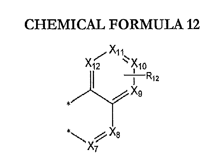
- Y may be represented by at least one of the following Chemical Formulae 2 to 12.
- R 2 to R 12 are independently selected from the group consisting of hydrogen, a C 1 to C 10 alkyl group, an amine group, a C 1 to C 10 alkylamine group, a C 1 to C 10 an alkoxy group, a C 2 to C 10 ester group, a nitro group, a cyano group, a C 6 to C 30 aryl group, a C 3 to C 20 heteroaryl group, a pyridyl group, and a halogen; and in Chemical Formulae 11 and 12, X 1 to X 12 are selected from the group consisting of a carbon atom, a nitrogen atom, an oxygen atom, a sulfur atom, and a phosphorus atom.
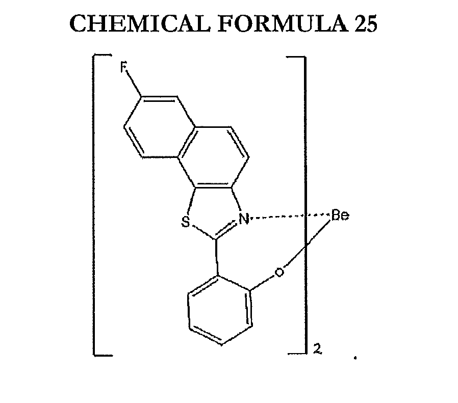
- the compound of Chemical Formula 1 may be selected from the following Chemical Formulae 13 to 25.
- the organic layer may further include at least one of the compounds represented by the following Chemical Formulae 13 to 25.
- the organic layer may be an organic emission layer, and the compound represented by the above Chemical Formula 1 may be a host material.
- the organic emission layer may further include a dopant material.
- the organic material may have improved carrier transport capability.
- the organic material may be used to provide an organic light emitting device having improved luminous efficiency and driving voltage characteristics.
- substituted refers to one substituted with a halogen (F, Br, Cl, or I), a hydroxy group, an alkoxy group, a nitro group, a cyano group, an amino group, an azido group, an amidino group, a hydrazino group, a hydtazono group, a carbonyl group, a carbamyl group, a thiol group, an ester group, a carboxyl group or a salt thereof, a sulfonic acid group or a salt thereof, a phosphoric acid group or a salt thereof, an alkyl group, a C 2 to C 16 alkenyl group, a C 2 to C 16 alkynyl group, a C 6 to C 30 aryl group, a C 7 to C 13 arylalkyl group, a C 1 to C 4 oxyalkyl group, a C 1 to C
- hetero refers to 1 to 3 heteroatoms selected from the group consisting of N, O, S, and P.
- the organic material may be applied to an organic emission layer, an auxiliary layer, or a combination thereof for an organic light emitting device.
- the auxiliary layer may include one of a hole injection layer (HIL), a hole transport layer, an electron injection layer (EIL), and an electron transport layer.
- the organic material includes a compound represented by Chemical Formula 1.
- A is an oxygen atom or a sulfur atom
- M is a divalent or trivalent metal
- R 1 is selected from the group consisting of hydrogen, a halogen (F, Br, Cl, or I), a hydroxy group, an alkoxy group, a nitro group, a cyano group, an amino group, an azido group, an amidino group, a hydrazino group, a hydrazono group, a carbonyl group, a carbamyl group, a thiol group, an ester group, a carboxyl group or a salt thereof, a sulfonic acid group or a salt thereof, a phosphoric acid group or a salt thereof, a C 1 to C 30 alkyl group, a C 2 to C 16 alkenyl group, a C 2 to C 16 alkynyl group, a C 6 to C 30 aryl group, a C 7 to C 13 arylalkyl group, a C 1 to C 4
- Y may be a substituted or unsubstituted C 3 to C 30 condensed polycyclic aromatic group (fused polycyclic aromatic group).
- the condensed polycyclic aromatic group may be a hydrocarbon-based condensed polycyclic aromatic group or a hetero condensed polycyclic aromatic group including a carbon atom, a nitrogen atom, an oxygen atom, a sulfur atom, a phosphorus atom, or a combination thereof.
- the hetero atom may be a nitrogen atom, an oxygen atom, a sulfur atom, a phosphorus atom, or a combination thereof.
- Z 1 to Z 4 are independently a carbon atom or a nitrogen atom, and n is 2 or 3.
- Substituent Y may have a substantially planar structure. Y may be positioned in the same plane as a hetero cycle including A and the nitrogen atom (N) of the above Chemical Formula 1. For example, Y may be selected from substituents represented by the following Chemical Formulae 2 to 12.
- R 2 to R 12 are independently selected from the group consisting of hydrogen, a C 1 to C 10 all ⁇ :yl group, an amine group, a C 1 to C 10 alkylamine group, a C 1 to C 10 alkoxy group, a C 2 to C 10 an ester group, a nitro group, a cyano group, a C 6 to C 30 aryl group, a C 3 to C 20 heteroaryl group, a pyridyl group, and a halogen
- X 1 to X 12 are selected from the group consisting of a carbon atom, a nitrogen atom, an oxygen atom, a sulfur atom, and a phosphorus atom.
- the organic material may include at least one of compounds represented by the following Chemical Formulae 13 to 25.
- Pi-electron systems of the hetero cycle including A and nitrogen (N) may be extended to an aromatic group of Y. Accordingly, an organic material including the compound may have improved electrical characteristics.
- an organic light emitting device including the organic material is described.
- the organic light emitting device includes a lower electrode 120, an upper electrode 160, and an organic emission layer 140 disposed between the lower electrode 120 and upper electrode 160.
- a lower auxiliary layer 130 may be interposed between the lower electrode 120 and the organic emission layer 140.
- An upper auxiliary layer 150 may be interposed between the organic emission layer 140 and the upper electrode 160.
- the substrate 110 may include glass, a polymer, or a combination thereof.
- At least one of the lower electrode 120 and the upper electrode 160 may be a cathode and the other one may be an anode.
- the lower electrode 120 and the upper electrode 160 may be a transparent or opaque electrode.
- the lower electrode 120 and the upper electrode 160 may include Indium Tin Oxide (ITO), Indium Zinc Oxide (IZO), or a combination thereof, or aluminum (Al), silver (Ag), or a combination thereof.
- At least one of the lower auxiliary layer 130 and the upper auxiliary layer 150 may include a hole injection layer (HIL) and/or a hole transport layer (HTL), and the other one may include an electron transport layer (ETL) and/or an electron injection layer (EIL).
- HIL hole injection layer
- ETL electron transport layer
- EIL electron injection layer
- the lower auxiliary layer 130 may include a hole injection layer (HIL) and/or a hole transport layer (HTL)
- the upper auxiliary layer 150 may include an electron injection layer (EIL) and/or an electron transport layer (ETL).
- EIL electron injection layer
- ETL electron transport layer
- at least one of the lower auxiliary layer 130 and the upper auxiliary layer 150 may be omitted.
- At least one of the lower auxiliary layer 130, the organic emission layer 140, and the upper auxiliary layer 150 may include the organic material.
- an organic material may be included as a host material in the organic emission layer 140.
- the organic material may improve electrical characteristics and luminous efficiency characteristics of organic light emitting devices.
- the compound represented by the above Chemical Formula 1 may have extended pi-electron systems by the aromatic groups of Y.
- the extended pi-election systems may improve carrier transport capability of the compound. Accordingly, the organic light emitting device including the compound represented by the above Chemical Formula 1 shows reduced driving electric power and improved luminous efficiency.
- the organic material may further include a dopant material.
- the organic material may further include a red dopant material, a green dopant material, a blue dopant material, or a combination thereof.
- Examples of the dopant material may include tris(1-phenylisoquinoline)iridium (Ir(piq)3), bis(2-phenylpyridine)iridium (ppy), bis(1-(phenyl)isoquinoline)iridium(III)acetylanetonate (Ir(phq)2acac), platinum(II)octaethylporphine (PtOEP), fac-tris(2-phenylpyridine)iridium (Ir(ppy)3), ttis(2-(1-cyclohexenyl)pyridine)iridium (Ir(chpy)3), tiis(2-(3-methyl-1-cyclohexenyl)pyridine)iridium (Ir(mchpy)3), iridium(III)bis(4,6-difluorophenyl)pyridinato-N,C-2'picolinate (Flrpic), iridium(III)
- FIGURE 2 another organic light emitting device including the organic material is described. Substantially equivalent constituent elements to constituent elements in FIGURE 1 are assigned the same reference numerals, which is not described hereinafter.
- organic emission layers 140 and 142 may include a plurality of laminated layers. The layers may emit different light from each other, and the laminated layers are combined with each other to emit white light. At least one of the organic emission layers 140 and 142 may include an organic material according to the first aspect of the present invention.
- the upper electrode 160 is disposed on the upper emission layer 140, and color filters 172, 174, and 176 are disposed on the upper electrode 160.
- White light emitted from the organic emission layers 140 and 142 may be converted into red, blue, and green colors after passing through the color filters 172, 174, and 176.
- color filters having different colors may be disposed on the upper electrode and different colors may be emitted.
- An Ag/ITO layer was disposed on a glass substrate and then patterned, preparing a lower electrode.
- N4,N4'-diphenyl-N4,N4'-bis(9-phenyl-9H-caxbazol-3-yl)biphenyl-4,4'-diamine and dipytazino2,3-f.2',3'-hquinoxaline hexacarbonitrile (HAT-CN) were disposed to be respectively 70 and 5nm thick to form a hole injection layer (HIL) on the lower electrode.
- N,N'-di(1-naphtyl)-N,N'-diphenyl-1,1'-biphenyl-4,4'-diamine was disposed to be 100nm thick as a hole transport layer (HTL) thereon.
- a mixture of a compound represented by the following Chemical Formula 13 and tiis(l-phenylisoquinoline)itidiutn (Ir(piq)3) was deposited to form an organic emission layer.
- the Ir(piq)3 was mixed in a concentration of 3 wt% with the compound represented by Chemical Formula 13.
- the compound represented by the above Chemical Formula 13 3 was used as a host material for an organic emission layer.
- the Ir(piq)3 was used as a dopant for an organic emission layer.
- ETL1 2-(4-(9,10-di(naphthalen-2-yl)anthracen-2-yl)phenyl)-1-phenyl-1H-benzoditnidazole)
- ETL2 8-hydioxyquinolinolato lithium
- An organic light emitting device including a red emission layer was fabricated according to the same method as Example 1, except for using a compound represented by the following Chemical Formula 14 as a host material.
- An organic light emitting device including a red emission layer was fabricated according to the same method as Example 1, except for using a compound represented by the following Chemical Formula 16 as a host material.
- An organic light emitting device including a red emission layer was fabricated according to the same method as Example 1, except for using a compound represented by the following Chemical Formula 17 as a host material.
- An organic light emitting device including a red emission layer was fabricated according to the same method as Example 1, except for using a compound represented by the following Chemical Formula 18 as a host material.
- An organic light emitting device including a red emission layer was fabricated according to the same method as Example 1, except for using a compound represented by the following Chemical Formula 19 as a host material.
- An organic light emitting device including a red emission layer was fabricated according to the same method as Example 1, except for using a compound represented by the following Chemical Formula 20 as a host material.
- An organic light emitting device including a red emission layer was fabricated according to the same method as Example 1, except for using a compound represented by the following Chemical Formula 21 as a host material.
- An organic light emitting device including a red emission layer was fabricated according to the same method as Example 1, except for using a compound represented by the following Chemical Formula 21 as a host material.
- An organic light emitting device including a red emission layer was fabricated according to the same method as Example 1, except for using biphenoxy-bis(8-hydroxy-3-methylquinoline)aluminium (BAlq) as a host material.
- BAlq biphenoxy-bis(8-hydroxy-3-methylquinoline)aluminium
- Example 1 The organic light emitting devices according to Examples 1 to 9 and Comparative Example 1 were measured regarding driving voltage (V) and current efficiency. The results are provided in the following Table 1. TABLE 1 Driving voltage (V) Current efficiency (cd/A) CIE x CIE y Maximum light emitting wavelength (nm) Example 1 3.9 36 0.658 0.342 624 Example 2 4.1 32 0.660 0.340 625 Example 3 4.2 31 0.661 0.339 625 Example 4 4.0 33 0.659 0.341 624 Example 5 4.0 32 0.658 0.341 624 Example 6 4.3 30 0.660 0.339 625 Example 7 3.8 37 0.656 0.343 623 Example 8 4.0 35 0.659 0.340 624 Example 9 4.5 29 0.660 0.341 625 Comparative Example 1 5.6 19 0.661 0.338 625
- the organic light emitting devices according to Examples 1 to 9 had a lower driving voltage than the one of Comparative Example 1. In addition, the organic light emitting devices according to Examples 1 to 9 had higher current efficiency than the one of Comparative Example 1.
- the organic light emitting devices of Examples 1 to 9 had substantially equal color quality to the one of Comparative Example 1.
- the organic light emitting devices according to Examples 1 to 9 turned out to emit light with substantially equal color quality at a low driving voltage with high current efficiency compared with the one of Comparative Example 1.
- a lower electrode glass was fabricated by disposing an Ag/ITO layer on a substrate and patterning it. Next, N4,N4'-diphenyl-N4,N4'-bis(9-phenyl-9H-carbazol-3-yl)biphenyl-4,4'-diamine and dipytazino2,3-f,2',3'-hquinoxaline hexacarbonitrile (HAT-CN) were laminated to be respectively about 70 and 5nm thick to form a hole injection layer (HIL) on the lower electrode.
- HAT-CN dipytazino2,3-f,2',3'-hquinoxaline hexacarbonitrile
- N,N'-di(l-naphtyl)-N,N'-diphenyl-1,1'-biphenyl-4,4'-diairline was laminated to be 100nm thick thereon as a hole transport layer (HTL).
- an organic emission layer was disposed thereon by depositing a mixture of a compound represented by the following Chemical Formula 15 and bis(2-phenylpyridine)iridium (ppy).
- the ppy was mixed in a concentration ratio of 3 wt% with the compound represented by Chemical Formula 15.
- the compound represented by the above Chemical Formula 15 was used as a host material for forming the organic emission layer, and the ppy was used as a dopant for forming the organic emission layer.
- ETL1 2-(4-(9,10-di(naphthalen-2-yl)anditacen-2-yl)phenyl)-l-phenyl-1H-benzodimidazole (ETL1) and 8-hydtoxyquinolinolato lithium (Liq) were deposited to be respectively about 30 and 0.5 nm thick, forming an electron transport layer (ETL) and an electron injection layer (EIL).
- ETL1 2-(4-(9,10-di(naphthalen-2-yl)anditacen-2-yl)phenyl)-l-phenyl-1H-benzodimidazole
- Liq 8-hydtoxyquinolinolato lithium
- An organic light emitting device including a green emission layer was fabricated according to the same method as Example 10, except for using 4,4'-N,N'-dicarbazole-biphenyl (CBP) as a host material.
- CBP 4,4'-N,N'-dicarbazole-biphenyl
- Example 10 The organic light emitting devices of Example 10 and Comparative Example 2 were measured regarding driving voltage (V) and current efficiency. The results are provided in the following Table 2. TABLE 2 Driving voltage (V) Current efficiency (cd/A) CIE x CIE y Maximum light emitting wavelength (nm) Example 10 5.1 34 0.342 0.601 521 Comparative Example 2 6.1 33 0.327 0.611 517
- the organic light emitting device of Example 10 had a lower driving voltage than the one of Comparative Example 2. Furthermore, the organic light emitting device of Example 10 had higher current efficiency than the one of Comparative Example 2.
- the organic light emitting devices of Example 10 and Comparative Example 2 had substantially equal color quality.
- the organic light emitting device of Example 10 emitted light with substantially equal color quality to the one of Comparative Example 2 at a low driving voltage with high current efficiency.
Landscapes
- Chemical & Material Sciences (AREA)
- Engineering & Computer Science (AREA)
- Materials Engineering (AREA)
- Organic Chemistry (AREA)
- Inorganic Chemistry (AREA)
- Physics & Mathematics (AREA)
- Optics & Photonics (AREA)
- Electroluminescent Light Sources (AREA)
- Plural Heterocyclic Compounds (AREA)
- Nitrogen And Oxygen Or Sulfur-Condensed Heterocyclic Ring Systems (AREA)
- Heterocyclic Carbon Compounds Containing A Hetero Ring Having Oxygen Or Sulfur (AREA)
Abstract

Description
- The present invention relates to an organic material for an organic light emitting device, and an organic light emitting device including the organic material.
- An organic light emitting device includes two electrodes facing each other and an organic layer interposed between the two electrodes. An organic light emitting device emits light when holes injected from one electrode are combined with electrons injected from the other electrode in an organic layer to produce excitons, and energy is released from the excitons. An organic light emitting device may be applied to various fields including display devices and illuminators.
- In an organic light emitting device, electric characteristics of a material in an organic layer may have a large effect on electrical characteristics of an organic light emitting device.
- In a first aspect of the present invention there is provided an organic material including a compound represented by the following Chemical Formula 1.

- In Chemical Formula 1, A is an oxygen (O) atom or a sulfur (S) atom; M is a divalent or trivalent metal atom; R1 is selected from the group consisting of hydrogen, a halogen (F, Br, Cl, or I), a hydroxy group, an alkoxy group, a nitro group, a cyano group, an amino group, an azido group, an amidino group, a hydrazino group, a hydrazono group, a carbonyl group, a carbamyl group, a thiol group, an ester group, a carboxyl group or a salt thereof, a sulfonic acid group or a salt thereof, a phosphoric acid group or a salt thereof, a C1 to C30 alkyl group, a C2 to C16 allenyl group, a C2 to C16 alkynyl group, a C6 to C30 aryl group, a C7 to C13 arylalkyl group, a C1 to C4 oxyalkyl group, a C1 to C20 heteroalkyl group, a C3 to C20 heteroarylalkyl group, a cycloalkyl group, a C3 to C15 cycloalkenyl group, a C6 to C15 cycloalkynyl group, and a heterocycloalkyl group; Y is a substituted or unsubstituted condensed polycyclic aromatic group; Z1 to Z4 are independently a carbon atom or a nitrogen atom; m is an integer ranging from 1 to 4; and n is 2 or 3.
- In a second aspect of the present invention there is provided an organic light emitting device that includes a first electrode and a second electrode facing each other, and an organic layer interposed between the first electrode and the second electrode. The organic layer includes a compound represented by the above Chemical Formula 1.
- In an embodiment, m is an integer of 2 or more, and R1's which are adjacent to each other may form a condensed ring.
- The condensed polycyclic aromatic group may be a hydrocarbon-based condensed polycyclic aromatic group or a hetero condensed polycyclic aromatic group including a carbon atom, a nitrogen atom, an oxygen atom, a sulfur atom, a phosphorus atom, or a combination thereof.
- In formula 1, Y may be represented by at least one of the following Chemical Formulae 2 to 12.


- In Chemical Formulae 2 to 12, R2 to R12 are independently selected from the group consisting of hydrogen, a C1 to C10 alkyl group, an amine group, a C1 to C10 alkylamine group, a C1 to C10 an alkoxy group, a C2 to C10 ester group, a nitro group, a cyano group, a C6 to C30 aryl group, a C3 to C20 heteroaryl group, a pyridyl group, and a halogen; and in Chemical Formulae 11 and 12, X1 to X12 are selected from the group consisting of a carbon atom, a nitrogen atom, an oxygen atom, a sulfur atom, and a phosphorus atom.
- The compound of Chemical Formula 1 may be selected from the following Chemical Formulae 13 to 25.


- The organic layer may further include at least one of the compounds represented by the following Chemical Formulae 13 to 25.


- The organic layer may be an organic emission layer, and the compound represented by the above Chemical Formula 1 may be a host material.
- The organic emission layer may further include a dopant material.
- An organic material having improved electrical characteristics is provided. The organic material may have improved carrier transport capability. The organic material may be used to provide an organic light emitting device having improved luminous efficiency and driving voltage characteristics.
- A more complete appreciation of the present invention, and many of the attendant advantages thereof, will be readily apparent as the same becomes better understood by reference to the following detailed description when considered in conjunction with the accompanying drawings, wherein:
-
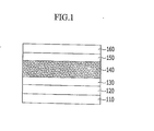
FIGURE 1 is a cross-sectional view showing an organic light emitting device according to an embodiment of the present invention; and -
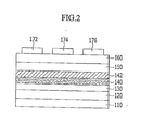
FIGURE 2 is a cross-sectional view showing an organic light emitting device according to an embodiment of the present invention. - As used herein, when a definition is not otherwise provided, the term "substituted" refers to one substituted with a halogen (F, Br, Cl, or I), a hydroxy group, an alkoxy group, a nitro group, a cyano group, an amino group, an azido group, an amidino group, a hydrazino group, a hydtazono group, a carbonyl group, a carbamyl group, a thiol group, an ester group, a carboxyl group or a salt thereof, a sulfonic acid group or a salt thereof, a phosphoric acid group or a salt thereof, an alkyl group, a C2 to C16 alkenyl group, a C2 to C16 alkynyl group, a C6 to C30 aryl group, a C7 to C13 arylalkyl group, a C1 to C4 oxyalkyl group, a C1 to C20 heteroalkyl group, a C3 to C20 heteroarylalkyl group, a cycloalkyl group, a C3 to C15 cycloalkenyl group, a C6 to C15 cycloalkynyl group, a heterocycloalkyl group, and a combination thereof instead of hydrogen.
- As used herein, when a definition is not otherwise provided, the term "hetero" refers to 1 to 3 heteroatoms selected from the group consisting of N, O, S, and P.
- In this specification, the term "and/or" refers to at least one of listed constituent elements. In this specification, constituent elements and/or portions are depicted using the words "first", "second", and the like, which are used for definite description.
- In this specification, it will be understood that when one constituent element is referred to as being "on" another constituent element, it can be directly on the other element of intervening elements may also be present.
- In the drawings, the thicknesses of constituent elements are exaggerated for clarity. The terms indicating positions such as "upper" and "under" are used for definite description of relative positions, and do not indicate absolute positions of constituent elements.
- Hereinafter, an organic material according to an embodiment is described.
- The organic material may be applied to an organic emission layer, an auxiliary layer, or a combination thereof for an organic light emitting device. The auxiliary layer may include one of a hole injection layer (HIL), a hole transport layer, an electron injection layer (EIL), and an electron transport layer.
- The organic material includes a compound represented by Chemical Formula 1.

- In Chemical Formula 1, A is an oxygen atom or a sulfur atom, M is a divalent or trivalent metal, R1 is selected from the group consisting of hydrogen, a halogen (F, Br, Cl, or I), a hydroxy group, an alkoxy group, a nitro group, a cyano group, an amino group, an azido group, an amidino group, a hydrazino group, a hydrazono group, a carbonyl group, a carbamyl group, a thiol group, an ester group, a carboxyl group or a salt thereof, a sulfonic acid group or a salt thereof, a phosphoric acid group or a salt thereof, a C1 to C30 alkyl group, a C2 to C16 alkenyl group, a C2 to C16 alkynyl group, a C6 to C30 aryl group, a C7 to C13 arylalkyl group, a C1 to C4 oxyalkyl group, a C1 to C20 heteroalkyl group, a C3 to C20 heteroarylalkyl group, a cycloalkyl group, a C3 to C15 cycloalkenyl group, a C6 to C15 cycloalkynyl group, and a heterocycloalkyl group, and m is an integer ranging from 1 to 4. In an embodiment, m is an integer of 2 or more, and R1's which are adjacent to each other may form a condensed ring.
- In Chemical Formula 1, Y may be a substituted or unsubstituted C3 to C30 condensed polycyclic aromatic group (fused polycyclic aromatic group). The condensed polycyclic aromatic group may be a hydrocarbon-based condensed polycyclic aromatic group or a hetero condensed polycyclic aromatic group including a carbon atom, a nitrogen atom, an oxygen atom, a sulfur atom, a phosphorus atom, or a combination thereof. The hetero atom may be a nitrogen atom, an oxygen atom, a sulfur atom, a phosphorus atom, or a combination thereof.
- In Chemical Formula 1, Z1 to Z4 are independently a carbon atom or a nitrogen atom, and n is 2 or 3.
- Substituent Y may have a substantially planar structure. Y may be positioned in the same plane as a hetero cycle including A and the nitrogen atom (N) of the above Chemical Formula 1. For example, Y may be selected from substituents represented by the following Chemical Formulae 2 to 12.
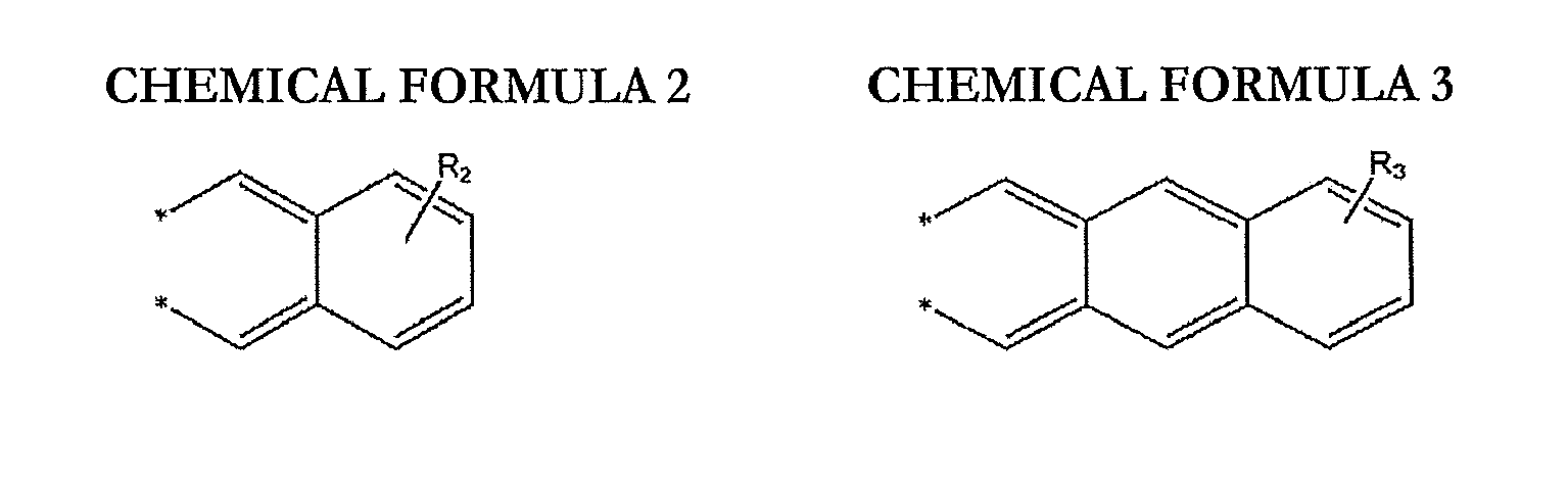


- In Chemical Formulae 2 to 12, R2 to R12 are independently selected from the group consisting of hydrogen, a C1 to C10 all\:yl group, an amine group, a C1 to C10 alkylamine group, a C1 to C10 alkoxy group, a C2 to C10 an ester group, a nitro group, a cyano group, a C6 to C30 aryl group, a C3 to C20 heteroaryl group, a pyridyl group, and a halogen, and in Chemical Formulae 11 and 12, X1 to X12 are selected from the group consisting of a carbon atom, a nitrogen atom, an oxygen atom, a sulfur atom, and a phosphorus atom.
- For example, the organic material may include at least one of compounds represented by the following Chemical Formulae 13 to 25.


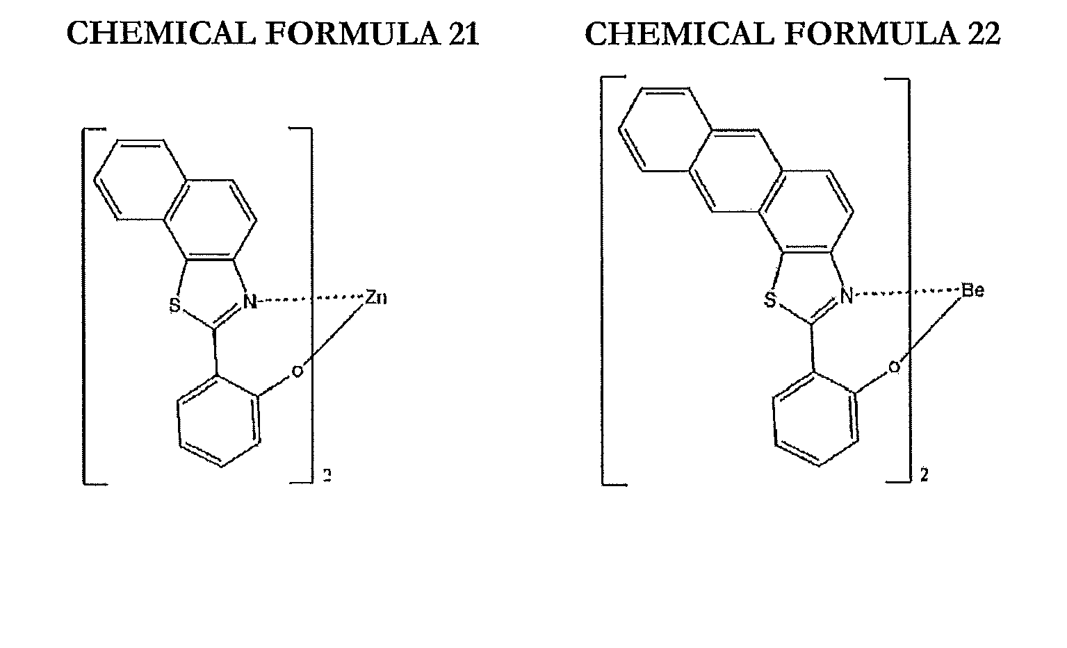


- Pi-electron systems of the hetero cycle including A and nitrogen (N) may be extended to an aromatic group of Y. Accordingly, an organic material including the compound may have improved electrical characteristics.
- Referring to
FIGURE 1 , an organic light emitting device including the organic material is described. - Referring to
FIGURE 1 , the organic light emitting device includes alower electrode 120, anupper electrode 160, and anorganic emission layer 140 disposed between thelower electrode 120 andupper electrode 160. A lowerauxiliary layer 130 may be interposed between thelower electrode 120 and theorganic emission layer 140. An upperauxiliary layer 150 may be interposed between theorganic emission layer 140 and theupper electrode 160. - The
substrate 110 may include glass, a polymer, or a combination thereof. - At least one of the
lower electrode 120 and theupper electrode 160 may be a cathode and the other one may be an anode. Thelower electrode 120 and theupper electrode 160 may be a transparent or opaque electrode. For example, thelower electrode 120 and theupper electrode 160 may include Indium Tin Oxide (ITO), Indium Zinc Oxide (IZO), or a combination thereof, or aluminum (Al), silver (Ag), or a combination thereof. - At least one of the lower
auxiliary layer 130 and the upperauxiliary layer 150 may include a hole injection layer (HIL) and/or a hole transport layer (HTL), and the other one may include an electron transport layer (ETL) and/or an electron injection layer (EIL). For example, when thelower electrode 120 is an anode and theupper electrode 150 is a cathode, the lowerauxiliary layer 130 may include a hole injection layer (HIL) and/or a hole transport layer (HTL) and the upperauxiliary layer 150 may include an electron injection layer (EIL) and/or an electron transport layer (ETL). However, at least one of the lowerauxiliary layer 130 and the upperauxiliary layer 150 may be omitted. - At least one of the lower
auxiliary layer 130, theorganic emission layer 140, and the upperauxiliary layer 150 may include the organic material. For example, an organic material may be included as a host material in theorganic emission layer 140. - The organic material may improve electrical characteristics and luminous efficiency characteristics of organic light emitting devices.
- The compound represented by the above Chemical Formula 1 may have extended pi-electron systems by the aromatic groups of Y. The extended pi-election systems may improve carrier transport capability of the compound. Accordingly, the organic light emitting device including the compound represented by the above Chemical Formula 1 shows reduced driving electric power and improved luminous efficiency.
- When the organic material is included in the
organic emission layer 140, the organic material may further include a dopant material. The organic material may further include a red dopant material, a green dopant material, a blue dopant material, or a combination thereof. - Examples of the dopant material may include tris(1-phenylisoquinoline)iridium (Ir(piq)3), bis(2-phenylpyridine)iridium (ppy), bis(1-(phenyl)isoquinoline)iridium(III)acetylanetonate (Ir(phq)2acac), platinum(II)octaethylporphine (PtOEP), fac-tris(2-phenylpyridine)iridium (Ir(ppy)3), ttis(2-(1-cyclohexenyl)pyridine)iridium (Ir(chpy)3), tiis(2-(3-methyl-1-cyclohexenyl)pyridine)iridium (Ir(mchpy)3), iridium(III)bis(4,6-difluorophenyl)pyridinato-N,C-2'picolinate (Flrpic), iridium(III) bis(4',6'-difluorophenylpyridinato)tetiakis (1-pyazoyl) borate (Fir6), or a combination thereof.
- Referring to
FIGURE 2 , another organic light emitting device including the organic material is described. Substantially equivalent constituent elements to constituent elements inFIGURE 1 are assigned the same reference numerals, which is not described hereinafter. - Referring to
FIGURE 2 ,organic emission layers organic emission layers - The
upper electrode 160 is disposed on theupper emission layer 140, andcolor filters upper electrode 160. White light emitted from theorganic emission layers color filters - The following examples illustrate this disclosure in more detail. These examples, however, are not in any sense to be interpreted as limiting the scope of this disclosure.
- An Ag/ITO layer was disposed on a glass substrate and then patterned, preparing a lower electrode. Next, N4,N4'-diphenyl-N4,N4'-bis(9-phenyl-9H-caxbazol-3-yl)biphenyl-4,4'-diamine and dipytazino2,3-f.2',3'-hquinoxaline hexacarbonitrile (HAT-CN) were disposed to be respectively 70 and 5nm thick to form a hole injection layer (HIL) on the lower electrode. Then, N,N'-di(1-naphtyl)-N,N'-diphenyl-1,1'-biphenyl-4,4'-diamine (NPD) was disposed to be 100nm thick as a hole transport layer (HTL) thereon.
- Then, a mixture of a compound represented by the following Chemical Formula 13 and tiis(l-phenylisoquinoline)itidiutn (Ir(piq)3) was deposited to form an organic emission layer. The Ir(piq)3 was mixed in a concentration of 3 wt% with the compound represented by Chemical Formula 13. The compound represented by the above Chemical Formula 13 3 was used as a host material for an organic emission layer. The Ir(piq)3 was used as a dopant for an organic emission layer.

- On the organic emission layer, 2-(4-(9,10-di(naphthalen-2-yl)anthracen-2-yl)phenyl)-1-phenyl-1H-benzoditnidazole) (ETL1) and 8-hydioxyquinolinolato lithium (Liq) were deposited to be respectively 30 and 0.5nm thick to form an electron transport layer (ETL) and an electron injection layer (EIL).
- Next, an Mg/Ag layer (a weight ratio of Mg:Ag = 160:10) was deposited to be 200nm thick, fabricating an upper electrode.
- In this way, an organic light emitting device including a red emission layer was fabricated.
- An organic light emitting device including a red emission layer was fabricated according to the same method as Example 1, except for using a compound represented by the following Chemical Formula 14 as a host material.

- An organic light emitting device including a red emission layer was fabricated according to the same method as Example 1, except for using a compound represented by the following Chemical Formula 16 as a host material.

- An organic light emitting device including a red emission layer was fabricated according to the same method as Example 1, except for using a compound represented by the following Chemical Formula 17 as a host material.

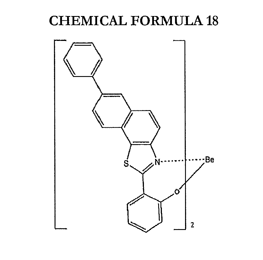
- An organic light emitting device including a red emission layer was fabricated according to the same method as Example 1, except for using a compound represented by the following Chemical Formula 18 as a host material.
- An organic light emitting device including a red emission layer was fabricated according to the same method as Example 1, except for using a compound represented by the following Chemical Formula 19 as a host material.

- An organic light emitting device including a red emission layer was fabricated according to the same method as Example 1, except for using a compound represented by the following Chemical Formula 20 as a host material.

- An organic light emitting device including a red emission layer was fabricated according to the same method as Example 1, except for using a compound represented by the following Chemical Formula 21 as a host material.

- An organic light emitting device including a red emission layer was fabricated according to the same method as Example 1, except for using a compound represented by the following Chemical Formula 21 as a host material.

- An organic light emitting device including a red emission layer was fabricated according to the same method as Example 1, except for using biphenoxy-bis(8-hydroxy-3-methylquinoline)aluminium (BAlq) as a host material.
- The organic light emitting devices according to Examples 1 to 9 and Comparative Example 1 were measured regarding driving voltage (V) and current efficiency. The results are provided in the following Table 1.
TABLE 1 Driving voltage (V) Current efficiency (cd/A) CIE x CIE y Maximum light emitting wavelength (nm) Example 1 3.9 36 0.658 0.342 624 Example 2 4.1 32 0.660 0.340 625 Example 3 4.2 31 0.661 0.339 625 Example 4 4.0 33 0.659 0.341 624 Example 5 4.0 32 0.658 0.341 624 Example 6 4.3 30 0.660 0.339 625 Example 7 3.8 37 0.656 0.343 623 Example 8 4.0 35 0.659 0.340 624 Example 9 4.5 29 0.660 0.341 625 Comparative Example 1 5.6 19 0.661 0.338 625 - Referring to Table 1, the organic light emitting devices according to Examples 1 to 9 had a lower driving voltage than the one of Comparative Example 1. In addition, the organic light emitting devices according to Examples 1 to 9 had higher current efficiency than the one of Comparative Example 1.
- Furthermore, referring to color quality evaluation through color coordinate and maximum light emitting wavelength measurements, the organic light emitting devices of Examples 1 to 9 had substantially equal color quality to the one of Comparative Example 1.
- The organic light emitting devices according to Examples 1 to 9 turned out to emit light with substantially equal color quality at a low driving voltage with high current efficiency compared with the one of Comparative Example 1.
- A lower electrode glass was fabricated by disposing an Ag/ITO layer on a substrate and patterning it. Next, N4,N4'-diphenyl-N4,N4'-bis(9-phenyl-9H-carbazol-3-yl)biphenyl-4,4'-diamine and dipytazino2,3-f,2',3'-hquinoxaline hexacarbonitrile (HAT-CN) were laminated to be respectively about 70 and 5nm thick to form a hole injection layer (HIL) on the lower electrode. Then, N,N'-di(l-naphtyl)-N,N'-diphenyl-1,1'-biphenyl-4,4'-diairline (NPD) was laminated to be 100nm thick thereon as a hole transport layer (HTL).
- Then, an organic emission layer was disposed thereon by depositing a mixture of a compound represented by the following Chemical Formula 15 and bis(2-phenylpyridine)iridium (ppy). The ppy was mixed in a concentration ratio of 3 wt% with the compound represented by Chemical Formula 15. The compound represented by the above Chemical Formula 15 was used as a host material for forming the organic emission layer, and the ppy was used as a dopant for forming the organic emission layer.

- On the organic emission layer, 2-(4-(9,10-di(naphthalen-2-yl)anditacen-2-yl)phenyl)-l-phenyl-1H-benzodimidazole (ETL1) and 8-hydtoxyquinolinolato lithium (Liq) were deposited to be respectively about 30 and 0.5 nm thick, forming an electron transport layer (ETL) and an electron injection layer (EIL).
- Then, an Mg/Ag layer (a weight ratio of Mg:Ag=160:10) was deposited to be 200 nm thick, fabricating an upper electrode.
- In this way, an organic light emitting device including a green emission layer was fabricated.
- An organic light emitting device including a green emission layer was fabricated according to the same method as Example 10, except for using 4,4'-N,N'-dicarbazole-biphenyl (CBP) as a host material.
- The organic light emitting devices of Example 10 and Comparative Example 2 were measured regarding driving voltage (V) and current efficiency. The results are provided in the following Table 2.
TABLE 2 Driving voltage (V) Current efficiency (cd/A) CIE x CIE y Maximum light emitting wavelength (nm) Example 10 5.1 34 0.342 0.601 521 Comparative Example 2 6.1 33 0.327 0.611 517 - Referring to Table 2, the organic light emitting device of Example 10 had a lower driving voltage than the one of Comparative Example 2. Furthermore, the organic light emitting device of Example 10 had higher current efficiency than the one of Comparative Example 2.
- In addition, referring to color quality evaluation through color coordinate and maximum light emitting wavelength measurements, the organic light emitting devices of Example 10 and Comparative Example 2 had substantially equal color quality.
- In other words, the organic light emitting device of Example 10 emitted light with substantially equal color quality to the one of Comparative Example 2 at a low driving voltage with high current efficiency.
- While the present embodiments has been described in connection with certain exemplary embodiments thereof, it is to be understood that the present invention is not limited to the disclosed embodiments, but, on the contrary, is intended to cover various modifications and equivalent arrangements included within the scope of the appended claims.
Claims (14)
- An organic material comprising a compound represented by the following Chemical Formula 1:

Y is a substituted or unsubstituted condensed polycyclic aromatic group;
Z1 to Z4 are independently a carbon atom or a nitrogen atom;
m is an integer from 1 to 4; and
n is 2 or 3. - The organic material of claim 1, wherein m is an integer of 2 or more, and at least two of the multiple instances of R1 adjacent to each other form a condensed ring.
- The organic material of claim 1 or claim 2, wherein the condensed polycyclic aromatic group is a hydtocarbon-based condensed polycyclic aromatic group or a hetero condensed polycyclic aromatic group including a carbon atom, a nitrogen atom, an oxygen atom, a sulfur atom, a phosphorus atom, or a combination thereof.
- The organic material of any of claims 1 to 3, wherein Y is represented by one of the following Chemical Formulae 2 to 12:


- The organic material of any of claims 1 to 4, wherein the compound of Chemical Formula 1is represented by one of the following Chemical Formulae 13 to 25:


- The organic material of claim 5, wherein the compound of Chemical Formula 1 is represented by Chemical Formula 13, chemical formula 17, chemical formula 18 or chemical formula 20:


- An organic light emitting device comprising:a first electrode and a second electrode facing each other; andan organic layer interposed between the first electrode and the second electrode,wherein the organic layer comprises a compound represented by the following Chemical Formula 1:

- The organic light emitting device of claim 7, wherein m is an integer of 2 of more, and at least two of the multiple instances of R1 adjacent to each other form a condensed ting.
- The organic light emitting device of claim 7 or claim 8, wherein the condensed polycyclic aromatic group is a hydrocarbon-based condensed polycyclic aromatic group or a hetero condensed polycyclic aromatic group including a carbon atom, a nitrogen atom, an oxygen atom, a sulfur atom, a phosphorus atom, or a combination thereof.
- The organic light emitting device of any of claims 7 to 9, wherein Y is represented by one of the following Chemical Formulae 2 to 12:


- The organic light emitting device of claim any of claims 7 to 10, wherein the compound of chemical formula 1 is represented by one of the following Chemical Formulae 13 to 25:


- The organic light emitting device of any of claims 7 to 11 wherein the organic layer is an organic emission layer and the compound of Chemical Formula 1 is a host material.
- The organic light emitting device of claim 12, wherein the organic emission layer further comprises a dopant material.
- The organic light emitting device of claim 11, wherein the compound of Chemical Formula 1 is represented by chemical formula 13, chemical formula 17, chemical formula 18, or chemical formula 20:


Applications Claiming Priority (1)
| Application Number | Priority Date | Filing Date | Title |
|---|---|---|---|
| KR1020100065452A KR20120004778A (en) | 2010-07-07 | 2010-07-07 | Organic materials and organic light emitting device comprising the same |
Publications (3)
| Publication Number | Publication Date |
|---|---|
| EP2404976A2 true EP2404976A2 (en) | 2012-01-11 |
| EP2404976A3 EP2404976A3 (en) | 2012-12-19 |
| EP2404976B1 EP2404976B1 (en) | 2014-06-25 |
Family
ID=44786155
Family Applications (1)
| Application Number | Title | Priority Date | Filing Date |
|---|---|---|---|
| EP11152765.1A Active EP2404976B1 (en) | 2010-07-07 | 2011-01-31 | Organic material and organic light emitting device including the same |
Country Status (5)
| Country | Link |
|---|---|
| US (1) | US8512881B2 (en) |
| EP (1) | EP2404976B1 (en) |
| JP (1) | JP5912259B2 (en) |
| KR (1) | KR20120004778A (en) |
| CN (1) | CN102311405A (en) |
Families Citing this family (9)
| Publication number | Priority date | Publication date | Assignee | Title |
|---|---|---|---|---|
| KR102021273B1 (en) * | 2011-05-27 | 2019-09-16 | 가부시키가이샤 한도오따이 에네루기 켄큐쇼 | Carbazole compound, light-emitting element, light-emitting device, electronic device, and lighting device |
| KR20140071897A (en) | 2012-11-26 | 2014-06-12 | 가부시키가이샤 한도오따이 에네루기 켄큐쇼 | Light-emitting element, light-emitting device, electronic device, and lighting device |
| CN104218157A (en) * | 2013-05-30 | 2014-12-17 | 海洋王照明科技股份有限公司 | Organic light emission diode device and fabrication method thereof |
| CN103319542B (en) * | 2013-07-21 | 2014-12-17 | 罗梅 | Chiral oxazoline cobalt complex and synthesis method thereof |
| CN103641787B (en) * | 2013-12-23 | 2015-07-15 | 罗梅 | Chiral oxazolinyl cobalt complex and synthesis method thereof |
| JP6511657B2 (en) * | 2014-09-03 | 2019-05-15 | 日本放送協会 | ORGANIC METAL COMPLEX, ORGANIC ELECTROLUMINESCENT DEVICE AND METHOD FOR MANUFACTURING THE SAME, DISPLAY DEVICE, LIGHTING DEVICE, ORGANIC THIN FILM SOLAR CELL |
| KR102331042B1 (en) * | 2015-08-31 | 2021-11-24 | 엘지디스플레이 주식회사 | Organic light emitting device |
| JP6635627B2 (en) * | 2019-02-05 | 2020-01-29 | 日本放送協会 | Organic electroluminescence element, method of manufacturing the same, display device, and lighting device |
| KR102824592B1 (en) * | 2021-09-27 | 2025-06-24 | 삼성전자주식회사 | Organometallic compound, organic light emitting device including the same and electronic apparatus comprising organic light emitting device |
Family Cites Families (12)
| Publication number | Priority date | Publication date | Assignee | Title |
|---|---|---|---|---|
| US5779937A (en) | 1995-05-16 | 1998-07-14 | Sanyo Electric Co., Ltd. | Organic electroluminescent device |
| JP3553689B2 (en) | 1995-05-16 | 2004-08-11 | 三洋電機株式会社 | Organic electroluminescence device |
| JP3389411B2 (en) | 1996-04-10 | 2003-03-24 | 三洋電機株式会社 | Organic electroluminescence device |
| JP3760508B2 (en) | 1996-06-10 | 2006-03-29 | 東洋インキ製造株式会社 | Organic electroluminescence device material and organic electroluminescence device using the same |
| JP2000100569A (en) | 1998-09-22 | 2000-04-07 | Toray Ind Inc | Light emitting element |
| JP2003082341A (en) * | 2001-09-07 | 2003-03-19 | Sharp Corp | Electroluminescent device |
| KR100707357B1 (en) * | 2005-06-23 | 2007-04-13 | (주)그라쎌 | Precursor Compounds of Organic Metal Complexes for Electroluminescent Materials |
| CN100361983C (en) * | 2005-12-16 | 2008-01-16 | 武汉大学 | Bidentate Ligands Containing Halogen Atoms and Their Iridium Complexes and Electrophosphorescent Devices |
| JP2007207916A (en) | 2006-01-31 | 2007-08-16 | Sanyo Electric Co Ltd | Organic EL display and organic EL element |
| CN101468973A (en) * | 2007-09-07 | 2009-07-01 | 葛来西雅帝史派有限公司 | Organometallic compounds for electroluminescence and organic electroluminescent device using the same |
| KR100850886B1 (en) | 2007-09-07 | 2008-08-07 | (주)그라쎌 | Organometallic compound for electroluminescence and display element employing it as light emitting material |
| KR100946409B1 (en) * | 2008-03-19 | 2010-03-09 | 다우어드밴스드디스플레이머티리얼 유한회사 | Novel organic light emitting compounds and organic electroluminescent devices employing the same as light emitting materials |
-
2010
- 2010-07-07 KR KR1020100065452A patent/KR20120004778A/en not_active Ceased
- 2010-10-26 US US12/912,628 patent/US8512881B2/en active Active
- 2010-12-02 CN CN2010105769854A patent/CN102311405A/en active Pending
-
2011
- 2011-01-31 EP EP11152765.1A patent/EP2404976B1/en active Active
- 2011-02-18 JP JP2011032790A patent/JP5912259B2/en active Active
Non-Patent Citations (1)
| Title |
|---|
| None |
Also Published As
| Publication number | Publication date |
|---|---|
| KR20120004778A (en) | 2012-01-13 |
| CN102311405A (en) | 2012-01-11 |
| US8512881B2 (en) | 2013-08-20 |
| EP2404976B1 (en) | 2014-06-25 |
| US20120007495A1 (en) | 2012-01-12 |
| EP2404976A3 (en) | 2012-12-19 |
| JP2012017449A (en) | 2012-01-26 |
| JP5912259B2 (en) | 2016-04-27 |
Similar Documents
| Publication | Publication Date | Title |
|---|---|---|
| KR102688384B1 (en) | Organic light emitting materials | |
| US12247150B2 (en) | Organic electroluminescent materials and devices | |
| EP2404976B1 (en) | Organic material and organic light emitting device including the same | |
| EP3205658B1 (en) | Organic electroluminescent materials and devices | |
| KR102635068B1 (en) | Organic electroluminescent materials and devices | |
| KR100803125B1 (en) | Red phosphorescent compound and organic light emitting device using the same | |
| KR101785755B1 (en) | Azaborine compounds as host materials and dopants for pholeds | |
| KR101761236B1 (en) | Siloles substituted with condensed ring systems and use thereof in organic electronics | |
| KR102582868B1 (en) | Organic electroluminescent materials and devices | |
| KR102642183B1 (en) | Novel organic compounds and organic light-emitting diode therewith | |
| TWI558718B (en) | Material for organic electroluminescent element and organic electroluminescent element using same | |
| JP4628435B2 (en) | Organic electroluminescence device | |
| KR102135228B1 (en) | Boron compound for organic electroluminescent elements, and organic electroluminescent element | |
| KR20150063462A (en) | Compound for organic electroluminescent elements, and organic electroluminescent element | |
| KR102583566B1 (en) | Novel compound and organic light emitting diode | |
| KR101833759B1 (en) | Novel spiro type organic compounds | |
| KR20150007605A (en) | Iridium complex and Organic light emitting device comprising the same | |
| KR102148870B1 (en) | An electroluminescent compound and an electroluminescent device comprising the same | |
| KR20230101151A (en) | Organic light emitting diode | |
| KR20110138721A (en) | Organic materials and organic light emitting device using the same | |
| KR102679314B1 (en) | organic light-emitting diode with High efficiency | |
| KR20160038988A (en) | Electron Transporting Compound Containing Electron Withdrawing Group and Organic emitting Device Employing The Same | |
| KR20070105080A (en) | Red phosphorescent compound and organic light emitting device using the same | |
| KR100662379B1 (en) | Red phosphorescent compound and organic light emitting device using the same | |
| KR20230101150A (en) | Organometallic compound and organic light emitting diode comprising the same |
Legal Events
| Date | Code | Title | Description |
|---|---|---|---|
| AK | Designated contracting states |
Kind code of ref document: A2 Designated state(s): AL AT BE BG CH CY CZ DE DK EE ES FI FR GB GR HR HU IE IS IT LI LT LU LV MC MK MT NL NO PL PT RO RS SE SI SK SM TR |
|
| AX | Request for extension of the european patent |
Extension state: BA ME |
|
| PUAI | Public reference made under article 153(3) epc to a published international application that has entered the european phase |
Free format text: ORIGINAL CODE: 0009012 |
|
| RAP1 | Party data changed (applicant data changed or rights of an application transferred) |
Owner name: SAMSUNG DISPLAY CO., LTD. |
|
| PUAL | Search report despatched |
Free format text: ORIGINAL CODE: 0009013 |
|
| AK | Designated contracting states |
Kind code of ref document: A3 Designated state(s): AL AT BE BG CH CY CZ DE DK EE ES FI FR GB GR HR HU IE IS IT LI LT LU LV MC MK MT NL NO PL PT RO RS SE SI SK SM TR |
|
| AX | Request for extension of the european patent |
Extension state: BA ME |
|
| RIC1 | Information provided on ipc code assigned before grant |
Ipc: H01L 51/50 20060101ALI20121112BHEP Ipc: C09K 11/06 20060101AFI20121112BHEP |
|
| 17P | Request for examination filed |
Effective date: 20130618 |
|
| RBV | Designated contracting states (corrected) |
Designated state(s): AL AT BE BG CH CY CZ DE DK EE ES FI FR GB GR HR HU IE IS IT LI LT LU LV MC MK MT NL NO PL PT RO RS SE SI SK SM TR |
|
| 17Q | First examination report despatched |
Effective date: 20130801 |
|
| GRAP | Despatch of communication of intention to grant a patent |
Free format text: ORIGINAL CODE: EPIDOSNIGR1 |
|
| INTG | Intention to grant announced |
Effective date: 20140116 |
|
| GRAS | Grant fee paid |
Free format text: ORIGINAL CODE: EPIDOSNIGR3 |
|
| GRAA | (expected) grant |
Free format text: ORIGINAL CODE: 0009210 |
|
| AK | Designated contracting states |
Kind code of ref document: B1 Designated state(s): AL AT BE BG CH CY CZ DE DK EE ES FI FR GB GR HR HU IE IS IT LI LT LU LV MC MK MT NL NO PL PT RO RS SE SI SK SM TR |
|
| REG | Reference to a national code |
Ref country code: GB Ref legal event code: FG4D |
|
| REG | Reference to a national code |
Ref country code: CH Ref legal event code: EP |
|
| REG | Reference to a national code |
Ref country code: AT Ref legal event code: REF Ref document number: 674727 Country of ref document: AT Kind code of ref document: T Effective date: 20140715 |
|
| REG | Reference to a national code |
Ref country code: IE Ref legal event code: FG4D |
|
| REG | Reference to a national code |
Ref country code: DE Ref legal event code: R096 Ref document number: 602011007863 Country of ref document: DE Effective date: 20140807 |
|
| PG25 | Lapsed in a contracting state [announced via postgrant information from national office to epo] |
Ref country code: GR Free format text: LAPSE BECAUSE OF FAILURE TO SUBMIT A TRANSLATION OF THE DESCRIPTION OR TO PAY THE FEE WITHIN THE PRESCRIBED TIME-LIMIT Effective date: 20140926 Ref country code: NO Free format text: LAPSE BECAUSE OF FAILURE TO SUBMIT A TRANSLATION OF THE DESCRIPTION OR TO PAY THE FEE WITHIN THE PRESCRIBED TIME-LIMIT Effective date: 20140925 Ref country code: LT Free format text: LAPSE BECAUSE OF FAILURE TO SUBMIT A TRANSLATION OF THE DESCRIPTION OR TO PAY THE FEE WITHIN THE PRESCRIBED TIME-LIMIT Effective date: 20140625 Ref country code: FI Free format text: LAPSE BECAUSE OF FAILURE TO SUBMIT A TRANSLATION OF THE DESCRIPTION OR TO PAY THE FEE WITHIN THE PRESCRIBED TIME-LIMIT Effective date: 20140625 Ref country code: CY Free format text: LAPSE BECAUSE OF FAILURE TO SUBMIT A TRANSLATION OF THE DESCRIPTION OR TO PAY THE FEE WITHIN THE PRESCRIBED TIME-LIMIT Effective date: 20140625 |
|
| REG | Reference to a national code |
Ref country code: AT Ref legal event code: MK05 Ref document number: 674727 Country of ref document: AT Kind code of ref document: T Effective date: 20140625 |
|
| REG | Reference to a national code |
Ref country code: NL Ref legal event code: VDEP Effective date: 20140625 |
|
| REG | Reference to a national code |
Ref country code: LT Ref legal event code: MG4D |
|
| PG25 | Lapsed in a contracting state [announced via postgrant information from national office to epo] |
Ref country code: RS Free format text: LAPSE BECAUSE OF FAILURE TO SUBMIT A TRANSLATION OF THE DESCRIPTION OR TO PAY THE FEE WITHIN THE PRESCRIBED TIME-LIMIT Effective date: 20140625 Ref country code: HR Free format text: LAPSE BECAUSE OF FAILURE TO SUBMIT A TRANSLATION OF THE DESCRIPTION OR TO PAY THE FEE WITHIN THE PRESCRIBED TIME-LIMIT Effective date: 20140625 Ref country code: SE Free format text: LAPSE BECAUSE OF FAILURE TO SUBMIT A TRANSLATION OF THE DESCRIPTION OR TO PAY THE FEE WITHIN THE PRESCRIBED TIME-LIMIT Effective date: 20140625 Ref country code: LV Free format text: LAPSE BECAUSE OF FAILURE TO SUBMIT A TRANSLATION OF THE DESCRIPTION OR TO PAY THE FEE WITHIN THE PRESCRIBED TIME-LIMIT Effective date: 20140625 |
|
| PG25 | Lapsed in a contracting state [announced via postgrant information from national office to epo] |
Ref country code: ES Free format text: LAPSE BECAUSE OF FAILURE TO SUBMIT A TRANSLATION OF THE DESCRIPTION OR TO PAY THE FEE WITHIN THE PRESCRIBED TIME-LIMIT Effective date: 20140625 Ref country code: RO Free format text: LAPSE BECAUSE OF FAILURE TO SUBMIT A TRANSLATION OF THE DESCRIPTION OR TO PAY THE FEE WITHIN THE PRESCRIBED TIME-LIMIT Effective date: 20140625 Ref country code: PT Free format text: LAPSE BECAUSE OF FAILURE TO SUBMIT A TRANSLATION OF THE DESCRIPTION OR TO PAY THE FEE WITHIN THE PRESCRIBED TIME-LIMIT Effective date: 20141027 Ref country code: EE Free format text: LAPSE BECAUSE OF FAILURE TO SUBMIT A TRANSLATION OF THE DESCRIPTION OR TO PAY THE FEE WITHIN THE PRESCRIBED TIME-LIMIT Effective date: 20140625 Ref country code: CZ Free format text: LAPSE BECAUSE OF FAILURE TO SUBMIT A TRANSLATION OF THE DESCRIPTION OR TO PAY THE FEE WITHIN THE PRESCRIBED TIME-LIMIT Effective date: 20140625 Ref country code: SK Free format text: LAPSE BECAUSE OF FAILURE TO SUBMIT A TRANSLATION OF THE DESCRIPTION OR TO PAY THE FEE WITHIN THE PRESCRIBED TIME-LIMIT Effective date: 20140625 |
|
| PG25 | Lapsed in a contracting state [announced via postgrant information from national office to epo] |
Ref country code: PL Free format text: LAPSE BECAUSE OF FAILURE TO SUBMIT A TRANSLATION OF THE DESCRIPTION OR TO PAY THE FEE WITHIN THE PRESCRIBED TIME-LIMIT Effective date: 20140625 Ref country code: IS Free format text: LAPSE BECAUSE OF FAILURE TO SUBMIT A TRANSLATION OF THE DESCRIPTION OR TO PAY THE FEE WITHIN THE PRESCRIBED TIME-LIMIT Effective date: 20141025 Ref country code: NL Free format text: LAPSE BECAUSE OF FAILURE TO SUBMIT A TRANSLATION OF THE DESCRIPTION OR TO PAY THE FEE WITHIN THE PRESCRIBED TIME-LIMIT Effective date: 20140625 Ref country code: AT Free format text: LAPSE BECAUSE OF FAILURE TO SUBMIT A TRANSLATION OF THE DESCRIPTION OR TO PAY THE FEE WITHIN THE PRESCRIBED TIME-LIMIT Effective date: 20140625 |
|
| REG | Reference to a national code |
Ref country code: DE Ref legal event code: R097 Ref document number: 602011007863 Country of ref document: DE |
|
| PG25 | Lapsed in a contracting state [announced via postgrant information from national office to epo] |
Ref country code: DK Free format text: LAPSE BECAUSE OF FAILURE TO SUBMIT A TRANSLATION OF THE DESCRIPTION OR TO PAY THE FEE WITHIN THE PRESCRIBED TIME-LIMIT Effective date: 20140625 Ref country code: IT Free format text: LAPSE BECAUSE OF FAILURE TO SUBMIT A TRANSLATION OF THE DESCRIPTION OR TO PAY THE FEE WITHIN THE PRESCRIBED TIME-LIMIT Effective date: 20140625 |
|
| PLBE | No opposition filed within time limit |
Free format text: ORIGINAL CODE: 0009261 |
|
| STAA | Information on the status of an ep patent application or granted ep patent |
Free format text: STATUS: NO OPPOSITION FILED WITHIN TIME LIMIT |
|
| 26N | No opposition filed |
Effective date: 20150326 |
|
| PG25 | Lapsed in a contracting state [announced via postgrant information from national office to epo] |
Ref country code: BE Free format text: LAPSE BECAUSE OF FAILURE TO SUBMIT A TRANSLATION OF THE DESCRIPTION OR TO PAY THE FEE WITHIN THE PRESCRIBED TIME-LIMIT Effective date: 20140625 |
|
| REG | Reference to a national code |
Ref country code: CH Ref legal event code: PL |
|
| PG25 | Lapsed in a contracting state [announced via postgrant information from national office to epo] |
Ref country code: LU Free format text: LAPSE BECAUSE OF FAILURE TO SUBMIT A TRANSLATION OF THE DESCRIPTION OR TO PAY THE FEE WITHIN THE PRESCRIBED TIME-LIMIT Effective date: 20150131 |
|
| PG25 | Lapsed in a contracting state [announced via postgrant information from national office to epo] |
Ref country code: MC Free format text: LAPSE BECAUSE OF FAILURE TO SUBMIT A TRANSLATION OF THE DESCRIPTION OR TO PAY THE FEE WITHIN THE PRESCRIBED TIME-LIMIT Effective date: 20140625 |
|
| PG25 | Lapsed in a contracting state [announced via postgrant information from national office to epo] |
Ref country code: LI Free format text: LAPSE BECAUSE OF NON-PAYMENT OF DUE FEES Effective date: 20150131 Ref country code: CH Free format text: LAPSE BECAUSE OF NON-PAYMENT OF DUE FEES Effective date: 20150131 |
|
| REG | Reference to a national code |
Ref country code: IE Ref legal event code: MM4A |
|
| PG25 | Lapsed in a contracting state [announced via postgrant information from national office to epo] |
Ref country code: SI Free format text: LAPSE BECAUSE OF FAILURE TO SUBMIT A TRANSLATION OF THE DESCRIPTION OR TO PAY THE FEE WITHIN THE PRESCRIBED TIME-LIMIT Effective date: 20140625 |
|
| REG | Reference to a national code |
Ref country code: FR Ref legal event code: PLFP Year of fee payment: 6 |
|
| PG25 | Lapsed in a contracting state [announced via postgrant information from national office to epo] |
Ref country code: IE Free format text: LAPSE BECAUSE OF NON-PAYMENT OF DUE FEES Effective date: 20150131 |
|
| REG | Reference to a national code |
Ref country code: FR Ref legal event code: PLFP Year of fee payment: 7 |
|
| PG25 | Lapsed in a contracting state [announced via postgrant information from national office to epo] |
Ref country code: MT Free format text: LAPSE BECAUSE OF FAILURE TO SUBMIT A TRANSLATION OF THE DESCRIPTION OR TO PAY THE FEE WITHIN THE PRESCRIBED TIME-LIMIT Effective date: 20140625 |
|
| PG25 | Lapsed in a contracting state [announced via postgrant information from national office to epo] |
Ref country code: SM Free format text: LAPSE BECAUSE OF FAILURE TO SUBMIT A TRANSLATION OF THE DESCRIPTION OR TO PAY THE FEE WITHIN THE PRESCRIBED TIME-LIMIT Effective date: 20140625 Ref country code: HU Free format text: LAPSE BECAUSE OF FAILURE TO SUBMIT A TRANSLATION OF THE DESCRIPTION OR TO PAY THE FEE WITHIN THE PRESCRIBED TIME-LIMIT; INVALID AB INITIO Effective date: 20110131 Ref country code: BG Free format text: LAPSE BECAUSE OF FAILURE TO SUBMIT A TRANSLATION OF THE DESCRIPTION OR TO PAY THE FEE WITHIN THE PRESCRIBED TIME-LIMIT Effective date: 20140625 |
|
| PG25 | Lapsed in a contracting state [announced via postgrant information from national office to epo] |
Ref country code: TR Free format text: LAPSE BECAUSE OF FAILURE TO SUBMIT A TRANSLATION OF THE DESCRIPTION OR TO PAY THE FEE WITHIN THE PRESCRIBED TIME-LIMIT Effective date: 20140625 |
|
| REG | Reference to a national code |
Ref country code: FR Ref legal event code: PLFP Year of fee payment: 8 |
|
| PG25 | Lapsed in a contracting state [announced via postgrant information from national office to epo] |
Ref country code: MK Free format text: LAPSE BECAUSE OF FAILURE TO SUBMIT A TRANSLATION OF THE DESCRIPTION OR TO PAY THE FEE WITHIN THE PRESCRIBED TIME-LIMIT Effective date: 20140625 |
|
| PG25 | Lapsed in a contracting state [announced via postgrant information from national office to epo] |
Ref country code: AL Free format text: LAPSE BECAUSE OF FAILURE TO SUBMIT A TRANSLATION OF THE DESCRIPTION OR TO PAY THE FEE WITHIN THE PRESCRIBED TIME-LIMIT Effective date: 20140625 |
|
| P01 | Opt-out of the competence of the unified patent court (upc) registered |
Effective date: 20230515 |
|
| PGFP | Annual fee paid to national office [announced via postgrant information from national office to epo] |
Ref country code: GB Payment date: 20251222 Year of fee payment: 16 |
|
| PGFP | Annual fee paid to national office [announced via postgrant information from national office to epo] |
Ref country code: FR Payment date: 20251223 Year of fee payment: 16 |
|
| PGFP | Annual fee paid to national office [announced via postgrant information from national office to epo] |
Ref country code: DE Payment date: 20251222 Year of fee payment: 16 |