EP2403078A2 - Beam combining light source - Google Patents
Beam combining light source Download PDFInfo
- Publication number
- EP2403078A2 EP2403078A2 EP11160785A EP11160785A EP2403078A2 EP 2403078 A2 EP2403078 A2 EP 2403078A2 EP 11160785 A EP11160785 A EP 11160785A EP 11160785 A EP11160785 A EP 11160785A EP 2403078 A2 EP2403078 A2 EP 2403078A2
- Authority
- EP
- European Patent Office
- Prior art keywords
- emitter
- beams
- row
- light
- light emitters
- Prior art date
- Legal status (The legal status is an assumption and is not a legal conclusion. Google has not performed a legal analysis and makes no representation as to the accuracy of the status listed.)
- Granted
Links
Images





Classifications
-
- H—ELECTRICITY
- H01—ELECTRIC ELEMENTS
- H01S—DEVICES USING THE PROCESS OF LIGHT AMPLIFICATION BY STIMULATED EMISSION OF RADIATION [LASER] TO AMPLIFY OR GENERATE LIGHT; DEVICES USING STIMULATED EMISSION OF ELECTROMAGNETIC RADIATION IN WAVE RANGES OTHER THAN OPTICAL
- H01S5/00—Semiconductor lasers
- H01S5/40—Arrangement of two or more semiconductor lasers, not provided for in groups H01S5/02 - H01S5/30
- H01S5/4012—Beam combining, e.g. by the use of fibres, gratings, polarisers, prisms
-
- H—ELECTRICITY
- H01—ELECTRIC ELEMENTS
- H01S—DEVICES USING THE PROCESS OF LIGHT AMPLIFICATION BY STIMULATED EMISSION OF RADIATION [LASER] TO AMPLIFY OR GENERATE LIGHT; DEVICES USING STIMULATED EMISSION OF ELECTROMAGNETIC RADIATION IN WAVE RANGES OTHER THAN OPTICAL
- H01S5/00—Semiconductor lasers
- H01S5/02—Structural details or components not essential to laser action
- H01S5/022—Mountings; Housings
- H01S5/023—Mount members, e.g. sub-mount members
- H01S5/02325—Mechanically integrated components on mount members or optical micro-benches
- H01S5/02326—Arrangements for relative positioning of laser diodes and optical components, e.g. grooves in the mount to fix optical fibres or lenses
-
- H—ELECTRICITY
- H01—ELECTRIC ELEMENTS
- H01S—DEVICES USING THE PROCESS OF LIGHT AMPLIFICATION BY STIMULATED EMISSION OF RADIATION [LASER] TO AMPLIFY OR GENERATE LIGHT; DEVICES USING STIMULATED EMISSION OF ELECTROMAGNETIC RADIATION IN WAVE RANGES OTHER THAN OPTICAL
- H01S5/00—Semiconductor lasers
- H01S5/005—Optical components external to the laser cavity, specially adapted therefor, e.g. for homogenisation or merging of the beams or for manipulating laser pulses, e.g. pulse shaping
-
- H—ELECTRICITY
- H01—ELECTRIC ELEMENTS
- H01S—DEVICES USING THE PROCESS OF LIGHT AMPLIFICATION BY STIMULATED EMISSION OF RADIATION [LASER] TO AMPLIFY OR GENERATE LIGHT; DEVICES USING STIMULATED EMISSION OF ELECTROMAGNETIC RADIATION IN WAVE RANGES OTHER THAN OPTICAL
- H01S5/00—Semiconductor lasers
- H01S5/005—Optical components external to the laser cavity, specially adapted therefor, e.g. for homogenisation or merging of the beams or for manipulating laser pulses, e.g. pulse shaping
- H01S5/0071—Optical components external to the laser cavity, specially adapted therefor, e.g. for homogenisation or merging of the beams or for manipulating laser pulses, e.g. pulse shaping for beam steering, e.g. using a mirror outside the cavity to change the beam direction
-
- H—ELECTRICITY
- H01—ELECTRIC ELEMENTS
- H01S—DEVICES USING THE PROCESS OF LIGHT AMPLIFICATION BY STIMULATED EMISSION OF RADIATION [LASER] TO AMPLIFY OR GENERATE LIGHT; DEVICES USING STIMULATED EMISSION OF ELECTROMAGNETIC RADIATION IN WAVE RANGES OTHER THAN OPTICAL
- H01S5/00—Semiconductor lasers
- H01S5/02—Structural details or components not essential to laser action
- H01S5/022—Mountings; Housings
- H01S5/0225—Out-coupling of light
- H01S5/02251—Out-coupling of light using optical fibres
-
- H—ELECTRICITY
- H01—ELECTRIC ELEMENTS
- H01S—DEVICES USING THE PROCESS OF LIGHT AMPLIFICATION BY STIMULATED EMISSION OF RADIATION [LASER] TO AMPLIFY OR GENERATE LIGHT; DEVICES USING STIMULATED EMISSION OF ELECTROMAGNETIC RADIATION IN WAVE RANGES OTHER THAN OPTICAL
- H01S5/00—Semiconductor lasers
- H01S5/40—Arrangement of two or more semiconductor lasers, not provided for in groups H01S5/02 - H01S5/30
- H01S5/4025—Array arrangements, e.g. constituted by discrete laser diodes or laser bar
- H01S5/4031—Edge-emitting structures
- H01S5/4043—Edge-emitting structures with vertically stacked active layers
- H01S5/405—Two-dimensional arrays
-
- H—ELECTRICITY
- H01—ELECTRIC ELEMENTS
- H01S—DEVICES USING THE PROCESS OF LIGHT AMPLIFICATION BY STIMULATED EMISSION OF RADIATION [LASER] TO AMPLIFY OR GENERATE LIGHT; DEVICES USING STIMULATED EMISSION OF ELECTROMAGNETIC RADIATION IN WAVE RANGES OTHER THAN OPTICAL
- H01S5/00—Semiconductor lasers
- H01S5/40—Arrangement of two or more semiconductor lasers, not provided for in groups H01S5/02 - H01S5/30
- H01S5/4025—Array arrangements, e.g. constituted by discrete laser diodes or laser bar
- H01S5/4031—Edge-emitting structures
- H01S5/4056—Edge-emitting structures emitting light in more than one direction
-
- H—ELECTRICITY
- H01—ELECTRIC ELEMENTS
- H01S—DEVICES USING THE PROCESS OF LIGHT AMPLIFICATION BY STIMULATED EMISSION OF RADIATION [LASER] TO AMPLIFY OR GENERATE LIGHT; DEVICES USING STIMULATED EMISSION OF ELECTROMAGNETIC RADIATION IN WAVE RANGES OTHER THAN OPTICAL
- H01S5/00—Semiconductor lasers
- H01S5/40—Arrangement of two or more semiconductor lasers, not provided for in groups H01S5/02 - H01S5/30
- H01S5/4025—Array arrangements, e.g. constituted by discrete laser diodes or laser bar
- H01S5/4075—Beam steering
Definitions
- the present invention generally relates to sources of optical radiation wherein light from multiple emitters is combined into a single output beam, and more specifically relates to combining polarized light from multiple laser or light emitting diodes into a single output beam for coupling into an optical fiber or waveguide.
- Semiconductor laser diodes manufactured as single emitter lasers or laser diode bars, have a high electrical-to-optical conversion efficiency, and can presently achieve optical power levels of a few Watts or even tens of Watts per single emitter laser diode, and tens to hundreds of Watts per laser diode bar. Due to high efficiency, reasonable power levels, and high spectral and directional brightness, laser diodes and laser diode bars find applications in many areas, such as material processing, offset printing, medical treatment, pumping of solid state lasers, and pumping of fiber lasers.
- light emitted from a high power single emitter diode laser is typically highly asymmetric due to a thin-slab geometry of the laser diodes resulting in long and thin emitting apertures.
- the light beam emitted by such lasers has much higher brightness in its "fast axis", which is perpendicular to the main p/n junctions and to the active layer of the laser, than in its "slow axis", which is parallel to the active layer.
- Many applications require that the light be coupled into an optical fiber, which generally has a substantially circular or polygonal cross-section and has a substantially symmetrical acceptance angle.
- light beams from multiple single emitter diode lasers are coupled into a single fiber stacked in their fast axis direction, as described for example in US Patents 6,898,222 , 7,668,214 , which are incorporated herein by reference, and US Patent Applications 2009/0245315 and 2009/0323752 , which are also incorporated herein by reference.
- an array of 3-10 individual laser emitters with a 100 micrometers (um) aperture width in the slow axis can be coupled into a fiber with a 105 um diameter and 0.15 NA (numerical aperture) by stacking individual laser beams in the fast axis direction.
- polarization beam combining may be used to couple light emitted by two arrays of single emitters into a single fiber, thereby doubling the power and brightness of the output beam.
- One example of such laser beam combining device which incorporates both the spatial stacking of equally polarized laser beams with polarization multiplexing of stacked beams from two laser arrays, is disclosed by Horikawa in U.S. Patent 4,978,197 , which is incorporated herein by reference.
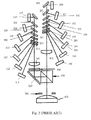
- the beam combining device of Horikawa is a substantially three-dimensional device and is illustrated in Fig. 1 . In this device, two rows of lasers 3 are positioned on an upper plate 2A of a multi-level support structure 2.
- a middle level plate 2B positioned beneath the upper plate 2A includes two rows of collimating lenses 4.
- the light beams emitted by the lasers 3 downwardly normally to the plates 2A and 2B, are collimated by the lenses 4, and then reflected by two rows of vertically offset prism mirrors 5 positioned on a lower plate 2C, to form two vertically stacked beams that are polarization combined using a polarization beam combiner (PBC) 7 and a half wave plate 9.
- PBC polarization beam combiner
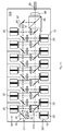
- U.S. Patent Application 2008/0198893 to Bartoschewski et al describes a laser assembly that is illustrated in Fig. 2 .
- this laser assembly light from two groups of vertically offset semiconductor lasers 100-106 and 107-113, each of the lasers incorporating a fast-axis collimator, is re-directed by two groups of mirrors 200-206 and 2007-213 along two parallel paths, wherein two slow-axis collimators 301 and 302 are positioned.
- the slow-axis collimated light beams are then combined using a PBC 400 and a half wave plate 500.
- the semiconductor lasers 100-113 in each of the two groups are oriented differently, and so are the reflectors 200-213 associated therewith.
- This arrangement although conserving space occupied by the assembly, can disadvantageously complicate the optical alignment of individual elements in the assembly, and its overall fabrication.
- An object of the present invention is to overcome at least some of the disadvantages of the prior art by providing a beam combining light source that would be compact, relatively easy to assemble and align, and would utilize polarization beam combining of light from multiple single emitters.
- the present invention relates to a beam combining light source, comprising: first and second rows of light emitters for emitting a plurality of first emitter beams and a plurality of second emitter beams, respectively; first and second rows of beam collimating reflectors for collimating the first and second emitter beams, respectively, and for re-directing thereof for forming first and second combined beams, wherein the first and second rows of beam collimating reflectors are spaced apart from the first and second rows of light emitters, respectively.
- the light emitters of the first and second rows are disposed in a staggered arrangement with a lateral offset therebetween.
- the second row of collimating reflectors is disposed at least partially in a space between the first row of light emitters and the first row of beam collimating reflectors, and the lateral offset between the first and second rows of the light emitters is such that the beam collimating reflectors of the second row do not block any of the first emitter beams.
- a feature of the present invention provides a plurality of fast axis collimators disposed at an output of the light emitters for collimating each of the first and second emitter beams in a fast axis plane.
- the light emitters are disposed in a plurality of levels, one light emitter of each of the first and second rows per level, said levels being mutually offset from each other in a direction of the fast axes, so that the first and second combined beams are composed of the emitter beams of the light emitters of the first and second row, respectively, which are stacked in the direction of the fast axes, and wherein the emitter beams of the light emitters disposed in a same level overlap in the polarization combined beam.
- An aspect of the present invention provides a beam combining light source, comprising: a first row of light emitters for emitting a plurality of first emitter beams along a plurality of optical paths, each of the first emitter beams having a fast axis and a slow axis; a first row of beam collimating reflectors for collimating each of the first emitter beams in a plane of the slow axis thereof, and for re-directing the first emitter beams to mutually align the fast axes thereof for forming a first combined beam, wherein the first row of beam collimating reflectors is disposed at a distance from the first row of light emitters defining a space therebetween; a second row of light emitters for emitting a plurality of second emitter beams along a plurality of optical paths, each of the second emitter beams having a fast axis and a slow axis; a second row of beam collimating reflectors spaced apart from the second row of light emitters for collimating
- a polarization converter is disposed in an optical path of one of the first and second combined beams for converting a polarization state thereof into a polarization state orthogonal to a polarization state of the other of the first and second combined beams.
- a polarization beam combiner is disposed for combining the first and second combined beams of light into a polarization combined beam of light.
- the light emitters of the first and second rows are disposed in a staggered arrangement with a lateral offset therebetween.
- the second row of collimating reflectors is disposed at least partially in the space between the first row of light emitters and the first row of collimating reflectors, and the lateral offset between the first and second rows of the light emitters is such that the collimating reflectors of the second row do not block any of the first emitter beams.
- An aspect of the present invention provides a method for fabricating a beam combining light source, comprising the steps of: a) providing a support base having a stepped surface comprising a series of parallel mounting surfaces disposed in a plurality of vertically offset levels; b) mounting a first set of light emitters upon the stepped surface of the support base, one light emitter of the first set per mounting surface, so as to form a first row of light emitters for emitting first emitter beams along parallel optical paths; c) mounting a second set of light emitters upon the stepped surface of the support base, one light emitter of the second set per mounting surface, so as to form a second row of light emitters for emitting second emitter beams along parallel optical paths, and so that light emitters of the first and second rows are disposed in a staggered arrangement with a lateral offset therebetween; d) mounting a plurality of beam collimating reflectors, one beam collimating reflector per light emitter of the first and second rows of light emitters, so as to
- Fig. 1 is a block diagram of a prior art beam combing optical source having a substantially three-dimensional layout
- Fig. 2 is a block diagram of a prior art beam combing optical source having a substantially planar layout
- Fig. 3A is a schematic plane view of an exemplary beam combing optical source according to a first embodiment of the invention
- Fig. 3B is a schematic front view of the exemplary beam combing optical source of Fig. 3A ;
- Fig. 3C is a front view of a single semiconductor light emitter with a broad emitting area
- Fig. 4A is a schematic cross-sectional view of a portion of the optical source of Fig. 3A taken along the line A-A in Fig. 3A illustrating cross-sections two emitter beams;
- Fig. 4B is a schematic cross-sectional view taken along the line B-B illustrating cross-sections of the combined beams prior to polarization combining htereof;
- Fig. 5A is a schematic plane view of an exemplary beam combing optical source according to a second embodiment of the invention.
- Fig. 5B is a schematic front view of the exemplary beam combing optical source of Fig. 5A ;
- Fig. 6A is a schematic plane view of an exemplary beam combing optical source according to a third embodiment of the invention.
- Fig. 6B is a schematic front view of the exemplary beam combing optical source of Fig. 6A ;
- Fig. 7 is a block diagram illustrating an embodiment of a beam collimating reflector
- Fig. 8A is a schematic plane view of an embodiment of a beam combing optical source having 14 single emitters
- Fig. 8B is a schematic diagram illustrating a cross-section of a combined beam produced in the apparatus of Fig. 8A ;
- Fig. 9A is a block diagram illustrating one alternative polarization multiplexing arrangement that can be used in the embodiments of Figs. 3A , 5A , 6A and 8A ;
- Fig. 9B is a block diagram illustrating another alternative polarization multiplexing arrangement that can be used in the embodiments of Figs. 3A , 5A , 6A and 8A .
- Fig. 10 is a schematic plane view of an exemplary beam combing optical source for outputting two beams of light formed of vertically stacked beams of two sets of light emitters.
- FIG. 3A and 3B there is shown, in plane and side views, respectively, one exemplary layout of an apparatus 222 for coupling radiation beams into an output port 99 such as an optical fiber or waveguide.
- the apparatus 222 will also be referred to herein as a beam combining optical source 222.
- the apparatus 222 is comprised of a plurality, in the shown exemplary embodiment - six, individual light emitters 20a to 20f, which are hereinafter generally referred to as emitters 20.
- the emitters 20 are arranged in two rows 301 and 302, with emitters 20a, 20b and 20c forming the first emitter row 301, and emitters 20d, 20e and 20f forming the second emitter row 302.
- the emitters 20 are mounted on a stepped surface 13 of a support 10 in several, in this embodiment - three, vertically offset levels, with one emitter 20 from each emitter row 301, 302 per step 13a, b, or per level.
- emitters 20a and 20d are mounted on a same top step 13a and are vertically offset from the rest of the emitters 20, emitters 20b and 20e are mounted on a same second top step 13b.
- longitudinal axes of opposing emitters of the first and second emitter rows are aligned.
- the steps 13a and 13b have straight edges 127 in the XZ plane 122A.
- the emitters 20 are spread along the X axis of the XZ plane 122A so as to enable efficient heat sinking into the support base 10 and efficient heat dissipation.
- emitters 20a - 20f emit light beams 33a -33f, respectively, which will be generally referred to as emitter beams 33.
- emitter beams 33 emitted by emitters 20 of each of the emitter rows 301, 302 are generally parallel to each other. It may also be generally preferred for ease of manufacturing that all the emitters 20 are oriented in parallel and emit parallel emitter beams 33.
- the light emitters 20 are planar devices, such as laser diodes or light emitting diodes that are each disposed with the plane of p/n junctions parallel to the XZ plane 122A of Fig.3A . In the shown exemplary embodiment they are mounted upon the stepped surface 13 with mounting pads 15, which provide electrical contact to the emitters 20 and thermal contact between emitters 20 and the support base 10.
- a front-facet view of one such emitter 20 is illustrated in Fig. 3C .
- the emitter 20 shown in Fig. 3C can be any of the emitters 20a-f of Figs. 3A and 3B , as well as any of the emitters 20 of other embodiments described hereinbelow.
- the emitters 20 may have a broad active area, with the emitting region 21 at a front facet of the emitter having the shape of a broad stripe, with a height b of for example about 1 ⁇ m in the vertical, i.e. Y axis direction that is normal to the XZ plane 122A of Fig. 3A and to the surface 13, and with the width a along X axis of the XZ plane 122A ranging for example from about 25 ⁇ m to about 200 ⁇ m or broader. Due to the long and narrow shape of the light emitting area 21 in such embodiments, properties of the beam 33 differ for the X and Y directions.
- the small height of the active region of the emitter results in a high beam divergence, for example about 25° FWHM or greater.
- the radiation of beam 33 in the fast axis direction which corresponds to the Y axis direction of the YZ plane 122B in Figs. 3B and 3C , may be approximately diffraction-limited with an M 2 factor only slightly above 1.
- the light may be distributed over many spatial modes, resulting in a beam divergence that is larger than for a diffraction-limited beam with that size, although still significantly smaller than for the fast axis direction, for example 5-15° FWHM divergence angle.
- the beam quality in terms of focusability is reduced, with M 2 factor that may be of the order of 20 for a 100- ⁇ m stripe width a.
- the apparatus 222 further includes fast axis collimators (FAC) 14, one per emitter 20, for collimating the emitter beams 33 in planes of their respective fast axes, which at the location of the FACs 14 are parallel to a YZ plane and orthogonal to plane XZ 122A of Fig. 3A .
- FAC fast axis collimators
- slow axis plane refers to a plane defined by the slow axis of a beam and the beam's propagation direction
- fast axis plane refers to a plane defined by the fast axis of a beam and the beam's propagation direction.
- Each of the FACs 14 is disposed at the output of a corresponding emitter 20 in a close proximity to the emission aperture thereof, and can be an optical lens that is cylindrical, or, more generally, toroidal in shape, such that while the divergence of beam 33 in a YZ plane, which is normal to the XZ plane 122A of Fig. 3A , is minimized or at least substantially reduced so that the beams 33 are collimated in their respective fast axis YZ planes after the FACs 14, the divergence of beams 33 in XZ plane 122A is nearly unaffected or affected to a lesser degree.
- the apparatus 222 further includes two rows 311 and 312 of beam collimating reflectors (BCR) 26a - 26f, one beam collimating reflector per emitter 20, which are generally referred to hereinbelow as collimating reflectors 26 or BCR 26.
- BCR beam collimating reflectors
- Each of the BCR 26 is coupled to, and optically aligned with, a different emitter 20, and in the shown embodiments is formed by a slow axis collimator (SAC) 30 optically followed by a turning reflector 40 that may be embodied as a flat mirror or other beam-deflecting device, such as but not limited to an optical prism or a diffraction grating.
- SAC slow axis collimator
- Each of the light beams 33 is collimated by a respective SAC 30 in the XZ plane 122A, and is then reflected in a general direction of a polarization beam combiner (PBC) 86.
- the SACs 26 can each be in the form of a cylindrical or toroidal lens as known in the art.
- the function of SACs 26 is to collimate the beams 33 in XZ plane 122A, such that the light beams 33 are collimated in both XZ plane 122A, i.e. the slow axis plane, and a YZ plane, i.e. the fast axis plane.
- the rows 311 and 312 of BCRs 26 are referred to herein as the first and the second BCR rows, respectively.
- the turning mirrors 40 are disposed to reflect the respective beams 33 in a generally same direction so as to mutually align the fast axes thereof in a YZ plane, thereby forming two combined beams of light 81 and 82.
- Each of the combined beams 81 and 82 is composed of vertically stacked collimated emitter beams 33 of the corresponding emitter row 301 or 302, with mutually aligned fast axes. Note that the term "vertical" is used herein to refer to a direction along the Y coordinate that is normal to the plane of the main p/n junctions of the emitters 20 and to the XZ plane 122A of the Fig. 3 .
- Fig. 4A illustrates a cross-section by XY plane 122B of a portion of the apparatus 222, showing two emitter beams 33a and 33b radiated from adjacent emitters 20a and 20b of the first emitter row 301.
- the cross-section is taken along the line A-A in Fig.3A , just upstream from the respective SACs 30.
- Dotted lines '55a' and '55b' indicate the fast axes of the respective emitter beams 33a and 33b, while dotted lines '51a' and '51b' indicate the slow axes of the respective emitter beams 33a and 33b.
- the slow-axis planes of the emitters 33 within the respective emitter row are parallel to each other and are separated in the fast axes direction "Y" by the step height h of the stepped surface 13. Accordingly, the beams 33a and 33b, prior to impinging upon the respective BCRs, are mutually offset both in the vertical "Y" direction, to which the fast axes 55 are parallel, and in the horizontal direction "X" along the emitter rows 301, 302, to which the slow axes 51 are parallel.
- the beam width along the slow axes 51 is much greater than the beam height along the fast axes 55.
- the beams are offset by the step height h of the stepped surface 13 as indicated in Fig. 3B , which may be approximately equal to the beam height in the vertical direction after the FAC 14, or at the entrance of the PBC 86.
- Fig. 4B illustrate a cross-section of the combined beams 81 and 82 by an YZ plane 122C taken along the line B-B in Fig.3A .
- the combined beams 81 and 82 are composed of the emitter beams 33 from the first and second emitter rows 301 and 302, respectively.
- the constituent emitter beams 33 from emitters 20 of the respective emitter row are stacked vertically with their fast axes 55 aligned along a same line, resulting in a more square-like cross-section of the corresponding combined beam 81 or 82.
- each of the emitter beams 33a-c in the combined beam 81 is aligned in its slow axis 51 with a corresponding emitter beam 33d-f in the combined beam 82, so that their slow-axis planes are coincident.
- emitter beams 33 emitted by opposing light emitters 20 in the apparatus 222 are pair-wise co-planar in their respective slow-axis planes.
- Each of the emitter beams 33 from the emitters 20 is polarized, having essentially same polarization state in the combined beams 81 and 82 in the B-B cross-section.
- a polarization converter 85 is provided in the optical path of one of the combined beams 81 and 82, for example in the optical path of the second combined beam 82 as shown in Fig. 3A , to convert its polarization state into an orthogonal polarization state.
- a beam redirector 87 embodied for example as a folding mirror, is further provided to re-direct one of the combined beams 81, 82 to intersect the other combined beam at a selected location, wherein the PBC 86 is disposed.
- the optical radiation in the combined beams 81 and 82 is linearly polarized
- the polarization converter 85 may be embodied as a half-wave plate
- the PBC 86 is a polarization beam combining cube having perpendicular beam receiving faces
- the folding mirror 87 is disposed in the optical path of the second combined beam 82 and is oriented to direct it to intersect the first combined beam 81 perpendicular thereto, i.e. at a 90° angle.
- the polarization converter 85, the folding mirror 87 and the PBC 86 together perform a polarization multiplexing of co-planar emitter beams 33 of the combined beams 81 and 82, outputting a polarization combined beam 83, which then can be coupled into the fiber 99 using a coupling optics 88, such as a suitable coupling lens, for example convex-convex or convex-plane, or an anamorphic telescope as known in the art.
- a coupling optics 88 such as a suitable coupling lens, for example convex-convex or convex-plane, or an anamorphic telescope as known in the art.
- the apparatus 222 of Figs. 3A and 3B has certain advantages with respect to those shown in Figs. 1 and 2 , such as enabling more simple assembly and optical alignment due to a generally planar arrangement wherein light emitters 33 in each of the rows, and optical elements 14, 26 associated therewith, are identically oriented. However, the apparatus 222 still has a relatively large footprint, which is related at least in part to a relatively large focal length of the SACs 30, as required to collimate the laser beams 33 in the slow axis plane.
- the light emitters 33 are wide-area laser diodes having a 100 ⁇ m wide emitting aperture, and the emitter beams 33 have an NA (numerical aperture) in the slow axis plane of approximately 0.15, requiring that there is a distance F of about 10 mm between each of the emitters 20 and the corresponding SAC 30.
- the resulting spatial separation of the emitters 20 and the corresponding collimating reflectors 26 creates an un-used space in the apparatus 222, such as the space ⁇ S' between the first emitter row 301 and the first BCR row 311, or more particularly between the FACs 14 and the corresponding SACs 30, as indicated in Fig 3A .
- FIG. 5A is a plan view, and a front view is shown in FIG. 5B .
- the apparatus 333 operates generally identically to the apparatus 222 as described hereinabove with reference to Figs. 3A-4B , and for illustrative purposes contains the same optical elements that the apparatus 222 of Figs. 3A and 3B , with like elements indicated using like reference labels.
- the apparatus 333 includes the first emitter row 301 composed of emitters 20a, 20b, 20c, and the second emitter row 302 composed of emitters 20d, 20e, 20f, which are supported by a support base 410 and are mounted on a stepped surface 413 thereof
- the emitters 20a, 20b, 20c of the first emitter row 301 emit beams 33a, 33b, and 33c, respectively hereinafter generally referred to as the first emitter beams
- the emitters 20d, 20e, 20f of the second emitter row 302 emit beams 33d, 33e, and 33f, respectively, hereinafter generally referred to as the second emitter beams.
- the first row 311 of BCRs 26, one per each light emitter 20 of the first emitter row 301, is provided for collimating each of the first emitter beams 33a, 33b and 33c in the plane of the slow axis thereof, and for re-directing the first emitter beams 33a-c to mutually align the fast axes thereof for forming the first combined beam 82.
- the second row 312 of BCRs 26 is provided for collimating each of the second emitter beams 33d-f in the planes of their respective slow axes, and for re-directing the second light beams 33d-f so as to mutually align the fast axes thereof for forming the second combined beam 82.
- first and second rows 311, 312 individual BCRs 26 are aligned with respective individual emitters 20 of either the first or the second emitter row 301, 302, and are separated therefrom by the distance F that is defined by the focal length of the SAC 30.
- the first and second BCR rows 311 and 312 of BCRs 26 are disposed generally in parallel to the first and second emitter rows 301 and 302, respectively, defining respective spaces therebetween.
- the FACs 14 are provided at the front facets of each of the emitters 20 for collimating the emitter beams 33 in the planes of their respective fast axes, which are directed along the Y axis normally to the XZ plane 422A.
- the FACs 14 may be provided with the emitters 20, for example attached thereto, and may be considered to be comprised therein.
- the light emitters 33 are wide-area laser diodes having a 100 ⁇ m wide emitting aperture, and the distance F between each of the emitters 20 and the corresponding SAC 30 is about 10 mm.
- the apparatus 333 has a more compact, space-conserving layout wherein the second row 312 of collimating reflectors 26 is disposed at least partially in the space ⁇ S' between the first emitter row 301 and the first BCR row 311 of collimating reflectors 26.
- the first and second emitter rows 301 and 302 are disposed with a lateral offset 31 therebetween, with the emitters 20 of the first and second emitter rows 301, 302 forming a staggered, or interleaved, emitter arrangement.
- the emitters 20d-f of the second emitter row 302 are located and aligned so that the second emitter beams 33d-f are directed to pass between BCRs 26a-c of the first BCR row 311, and the first emitter beams 33a-c are directed to path between BCRs 26d-f of the second BCR row 312.
- the stepped surface 413 may have somewhat different layout than the stepped surface 13 of the apparatus 222, with steps 413a, 413b having non-straight edges 128, although embodiments with straight step edges 128 are also possible.
- the lateral offset between same-level emitters 20 of the first and second emitter rows 302, 301 is approximately half of the distance between adjacent emitters 20 in each of the first and second rows.
- the emitters 20a-c of the first emitter row 301 may be spread along the X axis with a 8 mm spacing between their longitudinal axes, with the offset 31 being about 4 mm.
- the lateral offset 31 between same-level emitters of the first and second emitter rows 301, 302 may differ from half of the emitter spacing in the row, and is generally selected so that the collimating reflectors 26d-f of the second row 312 do not block any of the first light beams 33a-f.
- lateral indicates the direction along a row, such as from one emitter 20 within an emitter row 301 or 302 to another, and the term “lateral offset” is used to mean the distance between longitudinal axes of two emitters 20 located in a same level, e.g. mounted on a same step of the stepped surface 413.
- the emitters 20 are disposed in a plurality of levels 44, one light emitter 20 of each of the first and second emitter rows 301, 302 per level.
- the levels 44 are mutually offset from each other in the vertical direction, i.e. the direction of the fast axes of the emitters 20, which is also the Y axis direction of the YX plane 422B.
- the first and second combined beams 81, 82 are composed of the emitter beams 33a-c and 33d-f of the light emitters of the first and second row 301 and 302, respectively, which are stacked in the direction of the fast axes as illustrated in FIG. 4B .
- This vertically-offset arrangement of the emitters 20 is provided by the stepped surface 413 of the support base 410, upon which the emitters 20 are mounted.
- the stepped surface 413 is comprised of a sequence of parallel mounting surfaces such as those forming steps 413a and 413b of the stepped surface 413, the steps 413a,b having non-zero height h that is sufficient to enable the emitter beams of a higher level to pass over the BCRs of the lower level.
- Each of the steps 413a,b has one light emitter 20 from each of the first 301 and second 302 emitter rows mounted thereon, so that the planes of the slow axes of the respective emitter beams, such as emitter beams 33a and 33d, are coincident and parallel to the plane XZ 422A of the mounting surface 413.
- FIGs. 6A and 6B there is illustrated, in plane and front views, respectively, an apparatus 444 for combining light from a plurality of individual emitters according to another exemplary embodiment of the present invention.
- the apparatus 444 will also be referred to herein as a beam combining optical source 444.
- the apparatus 444 operates generally identically to the apparatus 333 and for illustration purposes includes same optical components, which will not be therefore further described, and which are mounted on a stepped surface 513 of a support base 510.
- the apparatus 444 provides another example of a compact beam combining layout with a reduced footprint, wherein the second BCR row 312 is disposed in the space between the first emitter row 301 and the first BCR row 311, and the first and second emitter rows 301, 302 have the lateral offset 31 therebetween, so as to form a staggered emitter arrangement.
- the second emitter row 302 is disposed behind the first emitter row 301, so that the first emitter row 310 is sandwiched between the second emitter row 302 and the second BCR row 312 coupled thereto.
- Emitters 20a-f of both emitter rows are facing, and emit light, in a same general direction, e.g.
- This device layout wherein all the emitters 20 are disposed close to one side of the mounting stepped surface 513 of the support base 510 facing the same direction, may provide some alignment advantages and a simplified device assembly, with a possible trade-off in heat sinking due to a smaller separation between emitters 20 of the first and second emitter rows 301, 302 and a less uniform distribution of the heat load across the mounting surface 513.
- the device layouts of the types illustrated in Figs. 5A and 6A enable to reduce the width of their respective devices by a factor of about 2 compared to the device layout of Fig. 3A .
- each of the aforedescribed embodiments may include other optical components, such as additional beam processing and beam shaping elements.
- the apparatus 444 is shown to include an optional Volume Bragg Grating (VBG) 89 disposed between the PBC 86 and the coupling lens 88 in the optical path of the polarization combined beam, for optionally providing an optical feedback to the emitters 20 for spectral locking thereof as known in the art.
- VBG Volume Bragg Grating
- Figs. 3A , 5A and 6A the BCRs 26 are shown to be each composed of the SAC 30 optically followed by the flat reflector 40, other embodiments of the BCRs 26 are also possible.
- Fig. 7 illustrate an embodiment wherein an emitter 20 is optically coupled to a BCR 26' wherein the SAC 30 is disposed optically after the flat mirror 40.
- the BCR 26 may be a single element, such as a curved cylindrical collimating mirror, which combines the functionalities of the FAC 30 and the flat mirror 40.
- Fig. 8A illustrates an embodiment wherein light from 14 emitters 20 is first combined into two combined beams, each of which comprised of 7 vertically staked emitter beams as illustrated in Fig. 8B so that the combined beam has an approximately square cross-section, and then polarization combined into a single output beam for coupling into the fiber 99.
- the half wave plate 85 or in more general case, the polarization converter 85 maybe disposed either before or after the folding mirror 87, or may also be disposed in the optical path of either the first or the second combined beam 81, 82.
- polarization multiplexing of the emitter beams 33 can also be accomplished using alternative configurations as known in the art. Two of such alternative configurations for polarization multiplexing of the combined beams 81 and 82 are illustrated in Figs. 9A and 9B . These configurations utilize walk-off crystals 96 and 96', respectively, to polarization combine the beams 81 and 82, after the polarization state of one of these beams has been converted to an orthogonal state.
- the first and second combined beams 81 and 82 impinge on the walk-off crystals 96 and 96' along parallel paths, and are polarization-combined by the respective walk-off crystals 96, 96' into the polarization combined beam 83 at the output of the crystal.
- the folding mirror 87 is absent.
- the folding mirror 87 is present, and an additional folding mirror 87' is added to bring the combined beams 81 and 82 closer together as they impinge upon the walk-off crystal 96', thereby enabling to reduce the size the walk-off crystal.
- Figs. 3A , 5A , 6A , 8A illustrate embodiments wherein the emitters 20 are all oriented with their optical axes perpendicular to the respective emitter rows 301, 302, i.e. perpendicular to the "X" direction, along which the emitters 20 are spread.
- this orientation is currently preferred as it simplifies the device assembly and minimizes the footprint
- embodiments wherein emitters 20 emit light at different angles with respect to the emitter rows would also be within the scope of the present invention.
- embodiments can be envisioned wherein the emitter rows 301 and 302 are curved rather than straight.
- the emitters 20 of each of the first and second emitter rows can all be disposed in a same level without a vertical offset therebetween.
- the respective emitter beams 33 emitted by emitters of each of the first and second emitter rows may, for example, be wavelength-multiplexed to form the combined beams 501 and 502 wherein the respective emitter beams overlap, for example using wavelength-selective elements in the BCRs 26 such as wavelength filters or wavelength-selective reflectors, and then polarization-multiplexed using the PBC 86 or alike.
- the beam combiner 86 and the beam redirector 87 can be omitted so as to result in a device that outputs two combined beams, each composed of vertically stacked beams of a plurality of planar light emitters.
- a beam combining apparatus 666 having two optical ports 99a and 99b.
- the apparatus 666 operates generally as described hereinabove with reference to Figs. 5a and 5b , so as to combine light beams from two sets of light emitters 301, 302 into two vertically-stacked combined beams 81, 82.
- the apparatus 666 lacks the polarization combining optical circuit of the apparatus 333 of Fig.
- the apparatus 666 includes first and second coupling optics 88a and 88b, which are disposed upon the base 410 in the optical paths of the two combined beams 81, 82, respectively, downstream from the respective BCR rows 311, 312,
- the coupling optics 88a,b are for coupling the combined beams 81, 82 into the two different optical fiber ports 99a, 99b.
- the apparatus 666 provides a compact dual-beam high-brightness light source that is characterized by a high optical-power-per-footprint ratio. It can be very useful in such applications as fiber laser pumping, where high-power high-brightness optical sources need to be fitted within a tightly size-controlled space.
- An aspect of the present invention provides a method for fabricating an optical beam combining apparatus, which includes the following general steps:
- first and second rows of beam collimating reflectors are optically coupled to and spaced apart from the first and second rows of light emitters, respectively, and wherein the second row of beam collimating reflectors is disposed at least partially in a space between the first row of light emitters and the first row of beam collimating reflectors, and wherein the lateral offset between the first and second rows of the light emitters is such that the beam collimating reflectors of the second row do not block any of the first emitter beams.
- the steps (b)-(d) are listed hereinabove not necessarily in the order in which they are performed during the device manufacturing, which may be varied as found convenient, and that one on the contrary the light emitters and the respective beam collimating reflectors can be mounted upon the base in any suitable order, and the steps of mounting maybe followed by optical alignment of the light emitters and the respective BCRs as known in the art.
- the step of mounting the light emitters may include first affixing the mounting pads 15 upon the mounting surfaces of the support base to provide thermal contact, and then affixing the light emitters 20 upon the mounting pads 15.
- An aspect of the present invention provides a beam combining light source, comprising: first and second rows of light emitters for emitting a plurality of first emitter beams and a plurality of second emitter beams, respectively; first and second rows of beam collimating reflectors for collimating the first and second emitter beams, respectively, and for re-directing thereof for forming first and second combined beams, wherein the first and second rows of beam collimating reflectors are optically coupled to and spaced apart from the first and second rows of light emitters, respectively; wherein the light emitters of the first and second rows are disposed in a staggered arrangement with a lateral offset therebetween, and wherein the second row of beam collimating reflectors is disposed at least partially in a space between the first row of light emitters and the first row of beam collimating reflectors, and the lateral offset between the first and second rows of the light emitters is such that the beam collimating reflectors of the second row do not block any of the first emitter beams.
- the emitter beams have each a fast axis and a slow axis
- the beam collimating reflectors are for collimating the emitter beams in planes of the slow axes thereof
- a plurality of fast axis collimators are provided for collimating each of the first and second emitter beams in a plane of the fast axis thereof.
- the beam combining light source further comprises a polarization beam combiner disposed for combining the first and second combined beams of light into a polarization combined beam of light.
Landscapes
- Physics & Mathematics (AREA)
- Condensed Matter Physics & Semiconductors (AREA)
- General Physics & Mathematics (AREA)
- Electromagnetism (AREA)
- Optics & Photonics (AREA)
- Semiconductor Lasers (AREA)
- Optical Couplings Of Light Guides (AREA)
Abstract
The multiplexed output beam is focused (88) into an optical fibre (99).
Description
- The present invention is a continuation-in-part of a United States
Patent Application 12/827,946 filed June 30, 2010 - The present invention generally relates to sources of optical radiation wherein light from multiple emitters is combined into a single output beam, and more specifically relates to combining polarized light from multiple laser or light emitting diodes into a single output beam for coupling into an optical fiber or waveguide.
- Semiconductor laser diodes, manufactured as single emitter lasers or laser diode bars, have a high electrical-to-optical conversion efficiency, and can presently achieve optical power levels of a few Watts or even tens of Watts per single emitter laser diode, and tens to hundreds of Watts per laser diode bar. Due to high efficiency, reasonable power levels, and high spectral and directional brightness, laser diodes and laser diode bars find applications in many areas, such as material processing, offset printing, medical treatment, pumping of solid state lasers, and pumping of fiber lasers.
- However, light emitted from a high power single emitter diode laser is typically highly asymmetric due to a thin-slab geometry of the laser diodes resulting in long and thin emitting apertures. The light beam emitted by such lasers has much higher brightness in its "fast axis", which is perpendicular to the main p/n junctions and to the active layer of the laser, than in its "slow axis", which is parallel to the active layer. Many applications require that the light be coupled into an optical fiber, which generally has a substantially circular or polygonal cross-section and has a substantially symmetrical acceptance angle. To obtain the highest brightness out of the fiber, light beams from multiple single emitter diode lasers are coupled into a single fiber stacked in their fast axis direction, as described for example in
US Patents 6,898,222 ,7,668,214 , which are incorporated herein by reference, andUS Patent Applications 2009/0245315 and2009/0323752 , which are also incorporated herein by reference. For example, an array of 3-10 individual laser emitters with a 100 micrometers (um) aperture width in the slow axis can be coupled into a fiber with a 105 um diameter and 0.15 NA (numerical aperture) by stacking individual laser beams in the fast axis direction. - Since the diode laser emission is typically polarized, polarization beam combining may be used to couple light emitted by two arrays of single emitters into a single fiber, thereby doubling the power and brightness of the output beam. One example of such laser beam combining device, which incorporates both the spatial stacking of equally polarized laser beams with polarization multiplexing of stacked beams from two laser arrays, is disclosed by Horikawa in
U.S. Patent 4,978,197 , which is incorporated herein by reference. The beam combining device of Horikawa is a substantially three-dimensional device and is illustrated inFig. 1 . In this device, two rows oflasers 3 are positioned on anupper plate 2A of a multi-level support structure 2. A middle level plate 2B positioned beneath theupper plate 2A includes two rows of collimatinglenses 4. The light beams emitted by thelasers 3 downwardly normally to theplates 2A and 2B, are collimated by thelenses 4, and then reflected by two rows of vertically offset prism mirrors 5 positioned on a lower plate 2C, to form two vertically stacked beams that are polarization combined using a polarization beam combiner (PBC) 7 and a half wave plate 9. One drawback of the device of Horikawa is that it is relatively bulky due to, at least in part, its essentially three-dimensional structure, which may also complicated assembly and alignment. Another drawback is that dissipating heat from the laser diodes may be more complicated. - In another example,
U.S. Patent Application 2008/0198893 to Bartoschewski et al describes a laser assembly that is illustrated inFig. 2 . In this laser assembly, light from two groups of vertically offset semiconductor lasers 100-106 and 107-113, each of the lasers incorporating a fast-axis collimator, is re-directed by two groups of mirrors 200-206 and 2007-213 along two parallel paths, wherein two slow-axis collimators PBC 400 and ahalf wave plate 500. - In the laser assembly of
Fig. 2 , the semiconductor lasers 100-113 in each of the two groups are oriented differently, and so are the reflectors 200-213 associated therewith. This arrangement, although conserving space occupied by the assembly, can disadvantageously complicate the optical alignment of individual elements in the assembly, and its overall fabrication. - An object of the present invention is to overcome at least some of the disadvantages of the prior art by providing a beam combining light source that would be compact, relatively easy to assemble and align, and would utilize polarization beam combining of light from multiple single emitters.
- Accordingly, the present invention relates to a beam combining light source, comprising: first and second rows of light emitters for emitting a plurality of first emitter beams and a plurality of second emitter beams, respectively; first and second rows of beam collimating reflectors for collimating the first and second emitter beams, respectively, and for re-directing thereof for forming first and second combined beams, wherein the first and second rows of beam collimating reflectors are spaced apart from the first and second rows of light emitters, respectively. The light emitters of the first and second rows are disposed in a staggered arrangement with a lateral offset therebetween. The second row of collimating reflectors is disposed at least partially in a space between the first row of light emitters and the first row of beam collimating reflectors, and the lateral offset between the first and second rows of the light emitters is such that the beam collimating reflectors of the second row do not block any of the first emitter beams.
- A feature of the present invention provides a plurality of fast axis collimators disposed at an output of the light emitters for collimating each of the first and second emitter beams in a fast axis plane.
- In accordance with a feature of the present invention, the light emitters are disposed in a plurality of levels, one light emitter of each of the first and second rows per level, said levels being mutually offset from each other in a direction of the fast axes, so that the first and second combined beams are composed of the emitter beams of the light emitters of the first and second row, respectively, which are stacked in the direction of the fast axes, and wherein the emitter beams of the light emitters disposed in a same level overlap in the polarization combined beam.
- An aspect of the present invention provides a beam combining light source, comprising: a first row of light emitters for emitting a plurality of first emitter beams along a plurality of optical paths, each of the first emitter beams having a fast axis and a slow axis; a first row of beam collimating reflectors for collimating each of the first emitter beams in a plane of the slow axis thereof, and for re-directing the first emitter beams to mutually align the fast axes thereof for forming a first combined beam, wherein the first row of beam collimating reflectors is disposed at a distance from the first row of light emitters defining a space therebetween; a second row of light emitters for emitting a plurality of second emitter beams along a plurality of optical paths, each of the second emitter beams having a fast axis and a slow axis; a second row of beam collimating reflectors spaced apart from the second row of light emitters for collimating each of the second emitter beams in a slow axis plane, and for re-directing the second emitter beams to mutually align the fast axes thereof for forming a second combined beam, wherein the fast axes of the first and second emitter beams in the first and second combined beams are parallel to each other. A polarization converter is disposed in an optical path of one of the first and second combined beams for converting a polarization state thereof into a polarization state orthogonal to a polarization state of the other of the first and second combined beams. A polarization beam combiner is disposed for combining the first and second combined beams of light into a polarization combined beam of light. The light emitters of the first and second rows are disposed in a staggered arrangement with a lateral offset therebetween. The second row of collimating reflectors is disposed at least partially in the space between the first row of light emitters and the first row of collimating reflectors, and the lateral offset between the first and second rows of the light emitters is such that the collimating reflectors of the second row do not block any of the first emitter beams.
- An aspect of the present invention provides a method for fabricating a beam combining light source, comprising the steps of: a) providing a support base having a stepped surface comprising a series of parallel mounting surfaces disposed in a plurality of vertically offset levels; b) mounting a first set of light emitters upon the stepped surface of the support base, one light emitter of the first set per mounting surface, so as to form a first row of light emitters for emitting first emitter beams along parallel optical paths; c) mounting a second set of light emitters upon the stepped surface of the support base, one light emitter of the second set per mounting surface, so as to form a second row of light emitters for emitting second emitter beams along parallel optical paths, and so that light emitters of the first and second rows are disposed in a staggered arrangement with a lateral offset therebetween; d) mounting a plurality of beam collimating reflectors, one beam collimating reflector per light emitter of the first and second rows of light emitters, so as to form first and second rows of beam collimating reflectors that are optically coupled to, and spaced apart from, the first and second rows of light emitters, respectively, for collimating the first and second emitter beams and for re-directing thereof for forming first and second combined beams composed of vertically stacked first and second emitter beams, respectively, and so that the second row of beam collimating reflectors is disposed at least partially in a space between the first row of light emitters and the first row of beam collimating reflectors coupled thereto. The lateral offset between the light emitters mounted upon a same mounting surface is such that the beam collimating reflectors of the second row do not block any of the first emitter beams.
- The invention will be described in greater detail with reference to the accompanying drawings which represent preferred embodiments thereof, in which like elements are indicated with like reference numerals, and wherein:
-
Fig. 1 is a block diagram of a prior art beam combing optical source having a substantially three-dimensional layout; -
Fig. 2 is a block diagram of a prior art beam combing optical source having a substantially planar layout; -
Fig. 3A is a schematic plane view of an exemplary beam combing optical source according to a first embodiment of the invention; -
Fig. 3B is a schematic front view of the exemplary beam combing optical source ofFig. 3A ; -
Fig. 3C is a front view of a single semiconductor light emitter with a broad emitting area; -
Fig. 4A is a schematic cross-sectional view of a portion of the optical source ofFig. 3A taken along the line A-A inFig. 3A illustrating cross-sections two emitter beams; -
Fig. 4B is a schematic cross-sectional view taken along the line B-B illustrating cross-sections of the combined beams prior to polarization combining htereof; -
Fig. 5A is a schematic plane view of an exemplary beam combing optical source according to a second embodiment of the invention; -
Fig. 5B is a schematic front view of the exemplary beam combing optical source ofFig. 5A ; -
Fig. 6A is a schematic plane view of an exemplary beam combing optical source according to a third embodiment of the invention; -
Fig. 6B is a schematic front view of the exemplary beam combing optical source ofFig. 6A ; -
Fig. 7 is a block diagram illustrating an embodiment of a beam collimating reflector; -
Fig. 8A is a schematic plane view of an embodiment of a beam combing optical source having 14 single emitters; -
Fig. 8B is a schematic diagram illustrating a cross-section of a combined beam produced in the apparatus ofFig. 8A ; -
Fig. 9A is a block diagram illustrating one alternative polarization multiplexing arrangement that can be used in the embodiments ofFigs. 3A ,5A ,6A and8A ; -
Fig. 9B is a block diagram illustrating another alternative polarization multiplexing arrangement that can be used in the embodiments ofFigs. 3A ,5A ,6A and8A . -
Fig. 10 is a schematic plane view of an exemplary beam combing optical source for outputting two beams of light formed of vertically stacked beams of two sets of light emitters. - While the present teachings are described in conjunction with various embodiments and examples, it is not intended that the present teachings be limited to such embodiments. On the contrary, the present teachings encompass various alternatives, modifications and equivalents, as will be appreciated by those of skill in the art. The terms "horizontal " and "vertical " are used exclusively with respect to the plane of the sheet. The terms "connect," "couple," "mount" and similar terms with their inflectional morphemes do not necessarily denote direct and immediate connections, but also include connections through mediate elements or devices.
- With reference to
Fig. 3A and3B , there is shown, in plane and side views, respectively, one exemplary layout of anapparatus 222 for coupling radiation beams into anoutput port 99 such as an optical fiber or waveguide. Theapparatus 222 will also be referred to herein as a beam combiningoptical source 222. Theapparatus 222 is comprised of a plurality, in the shown exemplary embodiment - six,individual light emitters 20a to 20f, which are hereinafter generally referred to asemitters 20. Theemitters 20 are arranged in tworows emitters first emitter row 301, andemitters second emitter row 302. Theemitters 20 are mounted on a steppedsurface 13 of asupport 10 in several, in this embodiment - three, vertically offset levels, with oneemitter 20 from eachemitter row step 13a, b, or per level. For example,emitters top step 13a and are vertically offset from the rest of theemitters 20,emitters top step 13b. In the shown embodiment, longitudinal axes of opposing emitters of the first and second emitter rows are aligned. Thesteps straight edges 127 in theXZ plane 122A. Within eachemitter row emitters 20 are spread along the X axis of theXZ plane 122A so as to enable efficient heat sinking into thesupport base 10 and efficient heat dissipation. - The
emitters 20a - 20f emitlight beams 33a -33f, respectively, which will be generally referred to as emitter beams 33. In one preferred configuration, emitter beams 33 emitted byemitters 20 of each of theemitter rows emitters 20 are oriented in parallel and emit parallel emitter beams 33. - In one embodiment the
light emitters 20 are planar devices, such as laser diodes or light emitting diodes that are each disposed with the plane of p/n junctions parallel to theXZ plane 122A ofFig.3A . In the shown exemplary embodiment they are mounted upon the steppedsurface 13 with mountingpads 15, which provide electrical contact to theemitters 20 and thermal contact betweenemitters 20 and thesupport base 10. A front-facet view of onesuch emitter 20 is illustrated inFig. 3C . Theemitter 20 shown inFig. 3C can be any of theemitters 20a-f ofFigs. 3A and3B , as well as any of theemitters 20 of other embodiments described hereinbelow. Theemitters 20 may have a broad active area, with the emittingregion 21 at a front facet of the emitter having the shape of a broad stripe, with a height b of for example about 1 µm in the vertical, i.e. Y axis direction that is normal to theXZ plane 122A ofFig. 3A and to thesurface 13, and with the width a along X axis of theXZ plane 122A ranging for example from about 25 µm to about 200 µm or broader. Due to the long and narrow shape of thelight emitting area 21 in such embodiments, properties of thebeam 33 differ for the X and Y directions. In the vertical (Y) direction, which is referred to as the fast axis direction, the small height of the active region of the emitter results in a high beam divergence, for example about 25° FWHM or greater. The radiation ofbeam 33 in the fast axis direction, which corresponds to the Y axis direction of theYZ plane 122B inFigs. 3B and 3C , may be approximately diffraction-limited with an M2 factor only slightly above 1. In the large width direction (X), also referred to as the slow axis direction, the light may be distributed over many spatial modes, resulting in a beam divergence that is larger than for a diffraction-limited beam with that size, although still significantly smaller than for the fast axis direction, for example 5-15° FWHM divergence angle. In the slow axis direction the beam quality in terms of focusability is reduced, with M2 factor that may be of the order of 20 for a 100-µm stripe width a. - Referring again to
Figs. 3A and3B , theapparatus 222 further includes fast axis collimators (FAC) 14, one peremitter 20, for collimating the emitter beams 33 in planes of their respective fast axes, which at the location of theFACs 14 are parallel to a YZ plane and orthogonal to planeXZ 122A ofFig. 3A . In this specification, the term "slow axis plane" refers to a plane defined by the slow axis of a beam and the beam's propagation direction, and the term "fast axis plane" refers to a plane defined by the fast axis of a beam and the beam's propagation direction. Each of theFACs 14 is disposed at the output of a correspondingemitter 20 in a close proximity to the emission aperture thereof, and can be an optical lens that is cylindrical, or, more generally, toroidal in shape, such that while the divergence ofbeam 33 in a YZ plane, which is normal to theXZ plane 122A ofFig. 3A , is minimized or at least substantially reduced so that thebeams 33 are collimated in their respective fast axis YZ planes after theFACs 14, the divergence ofbeams 33 inXZ plane 122A is nearly unaffected or affected to a lesser degree. - The
apparatus 222 further includes tworows emitter 20, which are generally referred to hereinbelow ascollimating reflectors 26 orBCR 26. Each of theBCR 26 is coupled to, and optically aligned with, adifferent emitter 20, and in the shown embodiments is formed by a slow axis collimator (SAC) 30 optically followed by a turningreflector 40 that may be embodied as a flat mirror or other beam-deflecting device, such as but not limited to an optical prism or a diffraction grating. Each of the light beams 33 is collimated by arespective SAC 30 in theXZ plane 122A, and is then reflected in a general direction of a polarization beam combiner (PBC) 86. TheSACs 26 can each be in the form of a cylindrical or toroidal lens as known in the art. The function ofSACs 26 is to collimate thebeams 33 inXZ plane 122A, such that the light beams 33 are collimated in bothXZ plane 122A, i.e. the slow axis plane, and a YZ plane, i.e. the fast axis plane. Therows BCRs 26 are referred to herein as the first and the second BCR rows, respectively. - In each of the first and
second BCR rows respective beams 33 in a generally same direction so as to mutually align the fast axes thereof in a YZ plane, thereby forming two combined beams oflight beams emitter row emitters 20 and to theXZ plane 122A of theFig. 3 . -
Fig. 4A illustrates a cross-section byXY plane 122B of a portion of theapparatus 222, showing twoemitter beams adjacent emitters first emitter row 301. The cross-section is taken along the line A-A inFig.3A , just upstream from therespective SACs 30. Dotted lines '55a' and '55b' indicate the fast axes of therespective emitter beams respective emitter beams emitter rows emitters 33 within the respective emitter row are parallel to each other and are separated in the fast axes direction "Y" by the step height h of the steppedsurface 13. Accordingly, thebeams emitter rows slow axes 51 are parallel. The beam width along theslow axes 51 is much greater than the beam height along the fast axes 55. In the vertical direction the beams are offset by the step height h of the steppedsurface 13 as indicated inFig. 3B , which may be approximately equal to the beam height in the vertical direction after theFAC 14, or at the entrance of thePBC 86. -
Fig. 4B illustrate a cross-section of the combinedbeams YZ plane 122C taken along the line B-B inFig.3A . The combined beams 81 and 82 are composed of the emitter beams 33 from the first andsecond emitter rows beams emitters 20 of the respective emitter row are stacked vertically with theirfast axes 55 aligned along a same line, resulting in a more square-like cross-section of the corresponding combinedbeam beam 81 is aligned in itsslow axis 51 with acorresponding emitter beam 33d-f in the combinedbeam 82, so that their slow-axis planes are coincident. In other words, emitter beams 33 emitted by opposinglight emitters 20 in theapparatus 222 are pair-wise co-planar in their respective slow-axis planes. - Each of the emitter beams 33 from the
emitters 20 is polarized, having essentially same polarization state in the combinedbeams polarization converter 85 is provided in the optical path of one of the combinedbeams beam 82 as shown inFig. 3A , to convert its polarization state into an orthogonal polarization state. Abeam redirector 87, embodied for example as a folding mirror, is further provided to re-direct one of the combinedbeams PBC 86 is disposed. In the illustrated embodiment, the optical radiation in the combinedbeams polarization converter 85 may be embodied as a half-wave plate, thePBC 86 is a polarization beam combining cube having perpendicular beam receiving faces, and thefolding mirror 87 is disposed in the optical path of the second combinedbeam 82 and is oriented to direct it to intersect the first combinedbeam 81 perpendicular thereto, i.e. at a 90° angle. Thepolarization converter 85, thefolding mirror 87 and thePBC 86 together perform a polarization multiplexing of co-planar emitter beams 33 of the combinedbeams beam 83, which then can be coupled into thefiber 99 using acoupling optics 88, such as a suitable coupling lens, for example convex-convex or convex-plane, or an anamorphic telescope as known in the art. - The
apparatus 222 ofFigs. 3A and3B has certain advantages with respect to those shown inFigs. 1 and2 , such as enabling more simple assembly and optical alignment due to a generally planar arrangement whereinlight emitters 33 in each of the rows, andoptical elements apparatus 222 still has a relatively large footprint, which is related at least in part to a relatively large focal length of theSACs 30, as required to collimate thelaser beams 33 in the slow axis plane. By way of example, thelight emitters 33 are wide-area laser diodes having a 100 µm wide emitting aperture, and the emitter beams 33 have an NA (numerical aperture) in the slow axis plane of approximately 0.15, requiring that there is a distance F of about 10 mm between each of theemitters 20 and thecorresponding SAC 30. The resulting spatial separation of theemitters 20 and the correspondingcollimating reflectors 26 creates an un-used space in theapparatus 222, such as the space `S' between thefirst emitter row 301 and thefirst BCR row 311, or more particularly between theFACs 14 and the correspondingSACs 30, as indicated inFig 3A . - Turning now to
Figs. 5A and5B , there is shown a schematic layout of a morecompact apparatus 333 for combining light from a plurality of individual emitters according to an exemplary embodiment of the present invention. Theapparatus 333 will also be referred to herein as a beam combiningoptical source 333.FIG. 5A is a plan view, and a front view is shown inFIG. 5B . Theapparatus 333 operates generally identically to theapparatus 222 as described hereinabove with reference toFigs. 3A-4B , and for illustrative purposes contains the same optical elements that theapparatus 222 ofFigs. 3A and3B , with like elements indicated using like reference labels. - Same as the
apparatus 222, theapparatus 333 includes thefirst emitter row 301 composed ofemitters second emitter row 302 composed ofemitters support base 410 and are mounted on a steppedsurface 413 thereof In operation, theemitters first emitter row 301 emitbeams emitters second emitter row 302 emitbeams first row 311 ofBCRs 26, one per eachlight emitter 20 of thefirst emitter row 301, is provided for collimating each of thefirst emitter beams first emitter beams 33a-c to mutually align the fast axes thereof for forming the first combinedbeam 82. Thesecond row 312 ofBCRs 26 is provided for collimating each of the second emitter beams 33d-f in the planes of their respective slow axes, and for re-directing the second light beams 33d-f so as to mutually align the fast axes thereof for forming the second combinedbeam 82. In each of the first andsecond rows individual BCRs 26 are aligned with respectiveindividual emitters 20 of either the first or thesecond emitter row SAC 30. In the shown embodiment, the first andsecond BCR rows BCRs 26 are disposed generally in parallel to the first andsecond emitter rows FACs 14 are provided at the front facets of each of theemitters 20 for collimating the emitter beams 33 in the planes of their respective fast axes, which are directed along the Y axis normally to theXZ plane 422A. In some embodiments, theFACs 14 may be provided with theemitters 20, for example attached thereto, and may be considered to be comprised therein. By way of example, thelight emitters 33 are wide-area laser diodes having a 100 µm wide emitting aperture, and the distance F between each of theemitters 20 and thecorresponding SAC 30 is about 10 mm. - In contrast to the
apparatus 222 ofFigs. 3A and3B , theapparatus 333 has a more compact, space-conserving layout wherein thesecond row 312 ofcollimating reflectors 26 is disposed at least partially in the space `S' between thefirst emitter row 301 and thefirst BCR row 311 of collimatingreflectors 26. To enable this space-conserving placement, the first andsecond emitter rows emitters 20 of the first andsecond emitter rows emitters 20d-f of thesecond emitter row 302 are located and aligned so that the second emitter beams 33d-f are directed to pass betweenBCRs 26a-c of thefirst BCR row 311, and thefirst emitter beams 33a-c are directed to path betweenBCRs 26d-f of thesecond BCR row 312. To enable this staggered emitter arrangement without substantially increasing the length of thesupport base 410 in the X direction along theemitter rows surface 413 may have somewhat different layout than the steppedsurface 13 of theapparatus 222, withsteps non-straight edges 128, although embodiments with straight step edges 128 are also possible. - In the shown exemplary embodiment, the lateral offset between same-
level emitters 20 of the first andsecond emitter rows adjacent emitters 20 in each of the first and second rows. By way of example, theemitters 20a-c of thefirst emitter row 301 may be spread along the X axis with a 8 mm spacing between their longitudinal axes, with the offset 31 being about 4 mm. However in other embodiments the lateral offset 31 between same-level emitters of the first andsecond emitter rows collimating reflectors 26d-f of thesecond row 312 do not block any of thefirst light beams 33a-f. Here, the term "lateral" indicates the direction along a row, such as from oneemitter 20 within anemitter row emitters 20 located in a same level, e.g. mounted on a same step of the steppedsurface 413. - As better shown in
Fig. 5B , theemitters 20 are disposed in a plurality oflevels 44, onelight emitter 20 of each of the first andsecond emitter rows levels 44 are mutually offset from each other in the vertical direction, i.e. the direction of the fast axes of theemitters 20, which is also the Y axis direction of theYX plane 422B. The first and second combinedbeams second row FIG. 4B . The emitter beams 33 of thelight emitters 20 that are disposed in a same one of thelevels 44 spatially overlap in the polarization combinedbeam 433, and mutually intersect prior to reaching thePBC 86. For example, theemitter beams corresponding BCRs 26d-f, intersect with the same-level emitter beams beam 81. - This vertically-offset arrangement of the
emitters 20 is provided by the steppedsurface 413 of thesupport base 410, upon which theemitters 20 are mounted. The steppedsurface 413 is comprised of a sequence of parallel mounting surfaces such as those formingsteps surface 413, thesteps 413a,b having non-zero height h that is sufficient to enable the emitter beams of a higher level to pass over the BCRs of the lower level. Each of thesteps 413a,b has onelight emitter 20 from each of the first 301 and second 302 emitter rows mounted thereon, so that the planes of the slow axes of the respective emitter beams, such asemitter beams plane XZ 422A of the mountingsurface 413. - Turning now to
Figs. 6A and6B , there is illustrated, in plane and front views, respectively, anapparatus 444 for combining light from a plurality of individual emitters according to another exemplary embodiment of the present invention. Theapparatus 444 will also be referred to herein as a beam combiningoptical source 444. Theapparatus 444 operates generally identically to theapparatus 333 and for illustration purposes includes same optical components, which will not be therefore further described, and which are mounted on a steppedsurface 513 of asupport base 510. - The
apparatus 444 provides another example of a compact beam combining layout with a reduced footprint, wherein thesecond BCR row 312 is disposed in the space between thefirst emitter row 301 and thefirst BCR row 311, and the first andsecond emitter rows Fig. 6A , however, thesecond emitter row 302 is disposed behind thefirst emitter row 301, so that the first emitter row 310 is sandwiched between thesecond emitter row 302 and thesecond BCR row 312 coupled thereto.Emitters 20a-f of both emitter rows are facing, and emit light, in a same general direction, e.g. in the Z-axis direction ofXZ plane 522A. This device layout, wherein all theemitters 20 are disposed close to one side of the mounting steppedsurface 513 of thesupport base 510 facing the same direction, may provide some alignment advantages and a simplified device assembly, with a possible trade-off in heat sinking due to a smaller separation betweenemitters 20 of the first andsecond emitter rows surface 513. - Advantageously, the device layouts of the types illustrated in
Figs. 5A and6A enable to reduce the width of their respective devices by a factor of about 2 compared to the device layout ofFig. 3A . - The aforedscribed embodiments of the invention are by way of example only, and many variations of the exemplary designs shown in
Figs. 3A to 6B are possible. - For example, each of the aforedescribed embodiments may include other optical components, such as additional beam processing and beam shaping elements. By way of example, the
apparatus 444 is shown to include an optional Volume Bragg Grating (VBG) 89 disposed between thePBC 86 and thecoupling lens 88 in the optical path of the polarization combined beam, for optionally providing an optical feedback to theemitters 20 for spectral locking thereof as known in the art. - Although in
Figs. 3A ,5A and6A theBCRs 26 are shown to be each composed of theSAC 30 optically followed by theflat reflector 40, other embodiments of theBCRs 26 are also possible. For example,Fig. 7 illustrate an embodiment wherein anemitter 20 is optically coupled to a BCR 26' wherein theSAC 30 is disposed optically after theflat mirror 40. In yet another embodiment, theBCR 26 may be a single element, such as a curved cylindrical collimating mirror, which combines the functionalities of theFAC 30 and theflat mirror 40. - Although the illustrated embodiments included only 6 emitters, the beam combining configuration is scalable, and other embodiments may include a greater number of emitters. By way of example,
Fig. 8A illustrates an embodiment wherein light from 14emitters 20 is first combined into two combined beams, each of which comprised of 7 vertically staked emitter beams as illustrated inFig. 8B so that the combined beam has an approximately square cross-section, and then polarization combined into a single output beam for coupling into thefiber 99. - Furthermore, the
half wave plate 85, or in more general case, thepolarization converter 85 maybe disposed either before or after thefolding mirror 87, or may also be disposed in the optical path of either the first or the second combinedbeam beams Figs. 9A and 9B . These configurations utilize walk-offcrystals 96 and 96', respectively, to polarization combine thebeams beams crystals 96 and 96' along parallel paths, and are polarization-combined by the respective walk-offcrystals 96, 96' into the polarization combinedbeam 83 at the output of the crystal. In the embodiment ofFig. 9A , thefolding mirror 87 is absent. In the embodiment ofFig. 9B , thefolding mirror 87 is present, and an additional folding mirror 87' is added to bring the combinedbeams - Furthermore,
Figs. 3A ,5A ,6A ,8A illustrate embodiments wherein theemitters 20 are all oriented with their optical axes perpendicular to therespective emitter rows emitters 20 are spread. Although this orientation is currently preferred as it simplifies the device assembly and minimizes the footprint, embodiments whereinemitters 20 emit light at different angles with respect to the emitter rows would also be within the scope of the present invention. Also, embodiments can be envisioned wherein theemitter rows emitters 20 of each of the first and second emitter rows can all be disposed in a same level without a vertical offset therebetween. In such embodiments, the respective emitter beams 33 emitted by emitters of each of the first and second emitter rows may, for example, be wavelength-multiplexed to form the combined beams 501 and 502 wherein the respective emitter beams overlap, for example using wavelength-selective elements in theBCRs 26 such as wavelength filters or wavelength-selective reflectors, and then polarization-multiplexed using thePBC 86 or alike. - In some embodiments of the invention, the
beam combiner 86 and thebeam redirector 87 can be omitted so as to result in a device that outputs two combined beams, each composed of vertically stacked beams of a plurality of planar light emitters. One such exemplary embodiment is illustrated inFig. 10 showing abeam combining apparatus 666 having twooptical ports apparatus 666 operates generally as described hereinabove with reference toFigs. 5a and5b , so as to combine light beams from two sets oflight emitters beams apparatus 666 lacks the polarization combining optical circuit of theapparatus 333 ofFig. 5A , formed by theelements apparatus 666 includes first andsecond coupling optics beams respective BCR rows coupling optics 88a,b are for coupling the combinedbeams optical fiber ports apparatus 666 provides a compact dual-beam high-brightness light source that is characterized by a high optical-power-per-footprint ratio. It can be very useful in such applications as fiber laser pumping, where high-power high-brightness optical sources need to be fitted within a tightly size-controlled space. - An aspect of the present invention provides a method for fabricating an optical beam combining apparatus, which includes the following general steps:
- a) providing a support base having a stepped surface comprising a series of parallel mounting surfaces disposed in a plurality of vertically offset levels;
- b) mounting a first set of light emitters upon the stepped surface of the support base, one light emitter of the first set per mounting surface, so as to form a first row of light emitters for emitting first emitter beams along parallel optical paths;
- c) mounting a second set of light emitters upon the stepped surface of the support base, one light emitter of the second set per mounting surface, so as to form a second row of light emitters for emitting second emitter beams along parallel optical paths, and so that light emitters of the first and second rows are disposed in a staggered arrangement with a lateral offset therebetween;
- d) mounting a plurality of beam collimating reflectors, one beam collimating reflector per light emitter of the first and second rows of light emitters, so as to form first and second rows of beam collimating reflectors for collimating the first and second emitter beams, respectively, and for re-directing thereof for forming first and second combined beams, wherein the first and second rows of beam collimating reflectors are optically coupled to and spaced apart from the first and second rows of light emitters, respectively, and wherein the second row of beam collimating reflectors is disposed at least partially in a space between the first row of light emitters and the first row of beam collimating reflectors, and wherein the lateral offset between the first and second rows of the light emitters is such that the beam collimating reflectors of the second row do not block any of the first emitter beams.
- It will be appreciated that the steps (b)-(d) are listed hereinabove not necessarily in the order in which they are performed during the device manufacturing, which may be varied as found convenient, and that one on the contrary the light emitters and the respective beam collimating reflectors can be mounted upon the base in any suitable order, and the steps of mounting maybe followed by optical alignment of the light emitters and the respective BCRs as known in the art. The step of mounting the light emitters may include first affixing the mounting
pads 15 upon the mounting surfaces of the support base to provide thermal contact, and then affixing thelight emitters 20 upon the mountingpads 15. - An aspect of the present invention provides a beam combining light source, comprising: first and second rows of light emitters for emitting a plurality of first emitter beams and a plurality of second emitter beams, respectively; first and second rows of beam collimating reflectors for collimating the first and second emitter beams, respectively, and for re-directing thereof for forming first and second combined beams, wherein the first and second rows of beam collimating reflectors are optically coupled to and spaced apart from the first and second rows of light emitters, respectively; wherein the light emitters of the first and second rows are disposed in a staggered arrangement with a lateral offset therebetween, and wherein the second row of beam collimating reflectors is disposed at least partially in a space between the first row of light emitters and the first row of beam collimating reflectors, and the lateral offset between the first and second rows of the light emitters is such that the beam collimating reflectors of the second row do not block any of the first emitter beams.
- In one embodiment the emitter beams have each a fast axis and a slow axis, the beam collimating reflectors are for collimating the emitter beams in planes of the slow axes thereof, a plurality of fast axis collimators are provided for collimating each of the first and second emitter beams in a plane of the fast axis thereof.
- In one embodiment the beam combining light source further comprises a polarization beam combiner disposed for combining the first and second combined beams of light into a polarization combined beam of light.
- While the foregoing description and drawings represent exemplary embodiments of the present invention, it will be obvious to those skilled in the art that various changes may be made therein without departing from the scope of the present invention as defined by the appended claims.
Claims (15)
- A beam combining light source, comprising:a support base;a first row of light emitters mounted upon the support base for emitting a plurality of first emitter beams along a plurality of optical paths, each of the first emitter beams having a fast axis and a slow axis;a first row of beam collimating reflectors mounted upon the support base for collimating each of the first emitter beams in a plane of the slow axis thereof, and for re-directing the first emitter beams to mutually align the fast axes thereof for forming a first combined beam, wherein the first row of beam collimating reflectors is disposed at a distance from the first row of light emitters defining a space therebetween;a second row of light emitters mounted upon the support base for emitting a plurality of second emitter beams along a plurality of optical paths, each of the second emitter beams having a fast axis and a slow axis;a second row of beam collimating reflectors mounted upon the support base and spaced apart from the second row of light emitters for collimating each of the second emitter beams in a slow axis plane, and for re-directing the second emitter beams to mutually align the fast axes thereof for forming a second combined beam;wherein light emitters of the first and second rows are disposed in a staggered arrangement with a lateral offset therebetween, and wherein:the second row of collimating reflectors is disposed at least partially in the space between the first row of light emitters and the first row of collimating reflectors, andthe lateral offset between the first and second rows of the light emitters is such that the collimating reflectors of the second row do not block any of the first emitter beams.
- The beam combining light source of claim 1, further comprising first and second coupling optics disposed upon the support based in optical paths of the first and second combined beams, respectfully, for coupling thereof into two optical fibers.
- The beam combining light source of claim 1, further comprising:a polarization converter disposed in an optical path of one of the first and second combined beams for converting a polarization state thereof into a polarization state orthogonal to a polarization state of the other of the first and second combined beams; and,a polarization beam combiner disposed for combining the first and second combined beams of light into a polarization combined beam of light.
- The beam combining light source of claim 3, wherein the light emitters are disposed in a plurality of levels, one light emitter of each of the first and second rows per level, said levels being mutually offset from each other in a direction of the fast axes, so that the first and second combined beams are composed of the first and second emitter beams, respectively, which are stacked in the direction of the fast axes thereof, and wherein the emitter beams of the light emitters disposed in a same level overlap in the polarization combined beam.
- The beam combining light source of claims 3 or 4, further comprising a coupling optics disposed downstream from the polarization beam combiner for focusing the polarization combined beam into an optical fiber.
- The beam combining light source of claim 5, further comprising a beam re-director disposed in an optical path of one of the first and second combined beams for re-directing thereof towards the polarization beam combiner.
- The beam combining light source of any of the claims 1 to 3 wherein the support base has a stepped surface comprised of a sequence of parallel mounting surfaces forming steps of the stepped surface, the steps having non-zero height, wherein each of the steps has at most two light emitters, one from each of the first and second rows of light emitters, mounted thereon with planes of the slow axes thereof parallel to the mounting surface, wherein each of the first and second combined beams of light is composed of the first or second emitter beams, respectively, which are stacked in a direction of the fast axes thereof.
- The beam combining light source of claim 7, wherein the first and second emitter beams of the light emitters mounted on a same step intersect.
- The beam combining light source of any of the claims 1 to 3, further comprising a plurality of fast axis collimators disposed at an output of the light emitters for collimating each of the first and second emitter beams in a fast axis plane.
- The beam combining light source of any of the claims 1 to 3, wherein the light emitters are spaced apart within each of the respective first and second rows, and are disposed to emit the first and second emitter beams generally perpendicular to the first and second rows of the light emitters.
- The beam combining light source of any of the claims 1 to 3, wherein each collimating reflector comprises a slow axis collimator and a turning mirror.
- The beam combining light source of any of the claims 1 to 3, wherein each light emitter comprises a broad area laser diode or a light emitting diode.
- The beam combining light source of any of the claims 1 to 3, wherein the light emitters of the first and second row are oriented facing a same general direction.
- The beam combining light source of any of the claims 1 to 3, wherein the emitters of the first and second rows are disposed for emitting the first and second emitter beams along parallel optical paths.
- A method for fabricating a beam combining light source, comprising:a) providing a support base having a stepped surface formed of a series of parallel mounting surfaces disposed in a plurality of vertically offset levels;b) mounting a first set of light emitters upon the stepped surface of the support base, one light emitter of the first set per mounting surface, so as to form a first row of light emitters for emitting first emitter beams along parallel optical paths;c) mounting a second set of light emitters upon the stepped surface of the support base, one light emitter of the second set per mounting surface, so as to form a second row of light emitters for emitting second emitter beams along parallel optical paths, and so that light emitters of the first and second rows are disposed in a staggered arrangement with a lateral offset between light emitters of the first and second sets mounted upon a same mounting surface;d) mounting a plurality of beam collimating reflectors, one beam collimating reflector per light emitter of the first and second rows of light emitters, so as to form first and second rows of beam collimating reflectors that are optically coupled to, and spaced apart from, the first and second rows of light emitters, respectively, for collimating the first and second emitter beams and for re-directing thereof for forming first and second combined beams, respectively, and so that the second row of beam collimating reflectors is disposed at least partially in a space between the first row of light emitters and the first row of beam collimating reflectors coupled thereto, and wherein the lateral offset between the light emitters mounted upon a same mounting surface is such that the beam collimating reflectors of the second row do not block any of the first emitter beams.
Applications Claiming Priority (1)
| Application Number | Priority Date | Filing Date | Title |
|---|---|---|---|
| US12/827,946 US8427749B2 (en) | 2010-06-30 | 2010-06-30 | Beam combining light source |
Publications (3)
| Publication Number | Publication Date |
|---|---|
| EP2403078A2 true EP2403078A2 (en) | 2012-01-04 |
| EP2403078A3 EP2403078A3 (en) | 2016-12-21 |
| EP2403078B1 EP2403078B1 (en) | 2023-10-25 |
Family
ID=44513226
Family Applications (1)
| Application Number | Title | Priority Date | Filing Date |
|---|---|---|---|
| EP11160785.9A Active EP2403078B1 (en) | 2010-06-30 | 2011-04-01 | Beam combining light source |
Country Status (2)
| Country | Link |
|---|---|
| US (1) | US8427749B2 (en) |
| EP (1) | EP2403078B1 (en) |
Cited By (3)
| Publication number | Priority date | Publication date | Assignee | Title |
|---|---|---|---|---|
| CN102590962A (en) * | 2012-02-22 | 2012-07-18 | 中国科学院半导体研究所 | Multiple unit semiconductor laser and optical fiber coupling system |
| US9243761B2 (en) | 2013-02-28 | 2016-01-26 | Sumitomo Electric Industries, Ltd. | Optical assembly and method for assembling the same, and optical module implemented with optical assembly |
| WO2016030970A1 (en) * | 2014-08-26 | 2016-03-03 | 住友電気工業株式会社 | Optical assembly |
Families Citing this family (50)
| Publication number | Priority date | Publication date | Assignee | Title |
|---|---|---|---|---|
| US8432945B2 (en) * | 2010-09-30 | 2013-04-30 | Victor Faybishenko | Laser diode combiner modules |
| US8891579B1 (en) | 2011-12-16 | 2014-11-18 | Nlight Photonics Corporation | Laser diode apparatus utilizing reflecting slow axis collimators |
| JP2013191787A (en) * | 2012-03-15 | 2013-09-26 | Sony Corp | Semiconductor laser array and semiconductor laser device |
| US9214786B2 (en) * | 2013-04-09 | 2015-12-15 | Nlight Photonics Corporation | Diode laser packages with flared laser oscillator waveguides |
| US9316846B2 (en) | 2013-07-11 | 2016-04-19 | Edmund L. Wolak | Systems and methods to provide high brightness diode laser outputs |
| US9647416B2 (en) * | 2013-12-23 | 2017-05-09 | Lumentum Operations Llc | Bidirectional long cavity semiconductor laser for improved power and efficiency |
| CN104734800B (en) * | 2013-12-24 | 2017-11-24 | 华为技术有限公司 | A kind of optical multiplexer and transmitting optical device |
| US9720145B2 (en) | 2014-03-06 | 2017-08-01 | Nlight, Inc. | High brightness multijunction diode stacking |
| US9705289B2 (en) | 2014-03-06 | 2017-07-11 | Nlight, Inc. | High brightness multijunction diode stacking |
| US10305252B2 (en) | 2014-10-15 | 2019-05-28 | Lumentum Operations Llc | Laser system and method of tuning the output power of the laser system |
| US9391425B2 (en) | 2014-10-17 | 2016-07-12 | Lumentum Operations Llc | Wavelength combined laser system |
| US20160119063A1 (en) | 2014-10-24 | 2016-04-28 | Lumentum Operations Llc | Wavelength locking and multiplexing of high-power semiconductor lasers |
| CN104538845B (en) * | 2014-12-30 | 2018-03-20 | 深圳市博锐浦科技有限公司 | More single-tube semiconductor laser fiber coupling packagings |
| US9209605B1 (en) | 2015-01-23 | 2015-12-08 | Lumentum Operations Llc | Laser diode subassembly and method of generating light |
| US10761276B2 (en) | 2015-05-15 | 2020-09-01 | Nlight, Inc. | Passively aligned crossed-cylinder objective assembly |
| CN105322435A (en) * | 2015-11-17 | 2016-02-10 | 山东圣达激光科技有限公司 | Double-end optical fiber-coupled output semiconductor laser device and laser system |
| JP6998774B2 (en) * | 2016-01-13 | 2022-02-10 | 古河電気工業株式会社 | Semiconductor laser devices, chip-on-submounts, and semiconductor laser modules |
| EP3417340A1 (en) | 2016-02-16 | 2018-12-26 | NLIGHT, Inc. | Passively aligned single element telescope for improved package brightness |
| WO2017161334A1 (en) | 2016-03-18 | 2017-09-21 | Nlight, Inc. | Spectrally multiplexing diode pump modules to improve brightness |
| US20180017735A1 (en) * | 2016-07-13 | 2018-01-18 | Futurewei Technologies, Inc. | Wavelength Division Multiplexer/Demultiplexer with Flexibility of Optical Adjustment |
| JP6316899B2 (en) * | 2016-10-17 | 2018-04-25 | ファナック株式会社 | Laser oscillator |
| US10054762B2 (en) * | 2016-12-06 | 2018-08-21 | Applied Optoelectronics, Inc. | Optical component holder having alignment feature for forming press-fit and an optical subassembly using same |
| WO2018119125A1 (en) | 2016-12-23 | 2018-06-28 | Nlight, Inc. | Low cost optical pump laser package |
| US10630041B2 (en) * | 2017-03-27 | 2020-04-21 | Nlight, Inc. | Beam offset plate for optically offsetting one or more laser beams |
| US10763640B2 (en) | 2017-04-24 | 2020-09-01 | Nlight, Inc. | Low swap two-phase cooled diode laser package |
| CN111512507A (en) * | 2017-11-01 | 2020-08-07 | 努布鲁有限公司 | Multi-kilowatt blue laser system |
| KR102007485B1 (en) | 2017-11-09 | 2019-08-06 | (주)코셋 | Circular type laser diode module combined optical fibers |
| CN111684330B (en) * | 2017-12-29 | 2021-10-26 | 南京镭芯光电有限公司 | Optical fiber photon engine |
| US10622787B2 (en) * | 2018-01-26 | 2020-04-14 | Pranalytica, Inc. | Dual quantum cascade laser micropackage |
| US10833482B2 (en) | 2018-02-06 | 2020-11-10 | Nlight, Inc. | Diode laser apparatus with FAC lens out-of-plane beam steering |
| CN109586163B (en) * | 2018-07-04 | 2020-11-03 | 深圳朗光科技有限公司 | Multi-single-tube high-power semiconductor laser packaging structure and laser |
| DE102018120112B4 (en) * | 2018-08-17 | 2026-05-07 | OSRAM Opto Semiconductors Gesellschaft mit beschränkter Haftung | Radiation-emitting component |
| JP7465149B2 (en) * | 2020-05-14 | 2024-04-10 | 株式会社フジクラ | Laser module and fiber laser device |
| US11710945B2 (en) * | 2020-05-25 | 2023-07-25 | Apple Inc. | Projection of patterned and flood illumination |
| DE102020118421B4 (en) * | 2020-07-13 | 2023-08-03 | Focuslight Technologies Inc. | laser device |
| CN111916991B (en) * | 2020-09-03 | 2025-10-31 | 无锡迈微光电科技有限公司 | Polarization type high-power laser |
| US11699715B1 (en) | 2020-09-06 | 2023-07-11 | Apple Inc. | Flip-chip mounting of optoelectronic chips |
| CN112260063B (en) * | 2020-10-20 | 2023-05-30 | 北京凯普林光电科技股份有限公司 | Single tube space beam combining device of semiconductor laser |
| CN112864792A (en) * | 2021-01-08 | 2021-05-28 | 西安炬光科技股份有限公司 | Semiconductor laser module and optical system |
| DE102021201606B4 (en) * | 2021-02-19 | 2022-10-06 | Osram Gmbh | ATTACHMENT FOR A LASER MODULE HAVING A LASER DIODE AND METHOD FOR MANUFACTURING THE LASER MODULE |
| US12431692B2 (en) | 2021-04-26 | 2025-09-30 | Lumentum Operations Llc | Multi-wavelength laser diode |
| JP7656188B2 (en) * | 2021-06-23 | 2025-04-03 | 日亜化学工業株式会社 | Semiconductor laser device |
| CN117546381A (en) * | 2021-07-16 | 2024-02-09 | 松下知识产权经营株式会社 | Single emitter stack for wavelength beam combining laser system |
| CN115343811A (en) * | 2022-04-21 | 2022-11-15 | 讯芸电子科技(中山)有限公司 | Butterfly type packaged optical transceiver |
| US12313812B2 (en) | 2022-09-20 | 2025-05-27 | Apple Inc. | MOE-based illumination projector |
| CN115954761A (en) * | 2022-09-28 | 2023-04-11 | 潍坊先进光电芯片研究院 | A multi-single-tube semiconductor laser beam combining device |
| CN116169556B (en) * | 2023-04-21 | 2023-07-04 | 深圳市星汉激光科技股份有限公司 | Optical fiber coupling semiconductor laser with ladder design and welding equipment |
| US12663596B2 (en) | 2023-05-22 | 2026-06-23 | Apple Inc. | Pattern projector |
| US12123589B1 (en) | 2023-05-22 | 2024-10-22 | Apple Inc. | Flood projector with microlens array |
| IL310710B2 (en) | 2024-02-07 | 2025-12-01 | Semiconductor Devices Ltd | Surface Beam-Based Laser System |
Citations (6)
| Publication number | Priority date | Publication date | Assignee | Title |
|---|---|---|---|---|
| US4978197A (en) | 1988-08-26 | 1990-12-18 | Fuji Photo Film Co., Ltd. | Beam-combining laser beam source device |
| US6898222B2 (en) | 2000-12-06 | 2005-05-24 | Jenoptik Laserdiode Gmbh | Diode laser arrangement with a plurality of diode laser arrays |
| US20080198893A1 (en) | 2005-08-19 | 2008-08-21 | Limo Patentverwaltung Gmbh & Co. Kg | Laser Assembly |
| US20090245315A1 (en) | 2008-03-28 | 2009-10-01 | Victor Faybishenko | Laser diode assemblies |
| US20090323752A1 (en) | 2008-06-26 | 2009-12-31 | Vadim Chuyanov | High brightness laser diode module |
| US7668214B2 (en) | 2007-06-12 | 2010-02-23 | Jds Uniphase Corporation | Light source |
Family Cites Families (24)
| Publication number | Priority date | Publication date | Assignee | Title |
|---|---|---|---|---|
| JPS63272092A (en) | 1987-04-30 | 1988-11-09 | Yoshiaki Arata | Forming method for superpowered composite laser beam |
| US4986634A (en) | 1988-08-26 | 1991-01-22 | Fuji Photo Film Co., Ltd. | Beam-combining laser beam source device |
| US5138491A (en) | 1988-08-26 | 1992-08-11 | Fuji Photo Film Co., Ltd. | Beam-combining laser beam source device |
| US5216544A (en) | 1988-08-26 | 1993-06-01 | Fuji Photo Film Co., Ltd. | Beam-combining laser beam source device |
| US5048911A (en) | 1988-11-15 | 1991-09-17 | Universiti Malaya | Coupling of multiple laser beams to a single optical fiber |
| US5185758A (en) | 1989-11-28 | 1993-02-09 | Massachusetts Institute Of Technology | Multiple-laser pump optical system |
| ES2142803T3 (en) | 1990-08-01 | 2000-05-01 | Diomed Ltd | HIGH POWER LIGHT SOURCE. |
| US5268978A (en) | 1992-12-18 | 1993-12-07 | Polaroid Corporation | Optical fiber laser and geometric coupler |
| DE19780124B4 (en) | 1996-02-23 | 2007-02-15 | Fraunhofer-Gesellschaft zur Förderung der angewandten Forschung e.V. | Arrangement for forming the geometric cross section of a plurality of solid-state and / or semiconductor lasers |
| DE19645150C2 (en) | 1996-10-28 | 2002-10-24 | Fraunhofer Ges Forschung | Optical arrangement for symmetrizing the radiation from laser diodes |
| US5933278A (en) | 1997-06-30 | 1999-08-03 | Polaroid Corporation | Monolithic multi-faceted mirror for combining multiple beams from different light sources by reflection |
| US6044096A (en) | 1997-11-03 | 2000-03-28 | Sdl, Inc. | Packaged laser diode array system and method with reduced asymmetry |
| US20020051360A1 (en) | 1998-11-04 | 2002-05-02 | Solodovnikov Vladimir Vadimovich | Method and apparatus for unifying light beams |
| US6005717A (en) | 1998-11-17 | 1999-12-21 | Ceramoptec Industries, Inc. | Diode laser beam combiner system |
| US6494371B1 (en) | 2000-03-09 | 2002-12-17 | Coherent, Inc. | Diode-laser light projector for illuminating a linear array of light modulators |
| JP2003198031A (en) * | 2001-12-26 | 2003-07-11 | Sumitomo Electric Ind Ltd | Light emitting module and optical amplifier |
| GB0312443D0 (en) | 2003-05-30 | 2003-07-09 | Newoptics Ltd | Optical multiplexer |
| US7006549B2 (en) | 2003-06-11 | 2006-02-28 | Coherent, Inc. | Apparatus for reducing spacing of beams delivered by stacked diode-laser bars |
| EP1771927A1 (en) | 2004-06-01 | 2007-04-11 | Trumpf Photonics, Inc. | Optimum matching of the output of a two-dimensional laser array stack to an optical fiber |
| DE202005009294U1 (en) * | 2005-06-13 | 2005-11-17 | Arctos Showlasertechnik E.Kfm. | Laser equipment for generation of laser beam has first partial laser beam device for producing red laser beam and second partial laser device for producing cyan laser beam whereby two beams are combined to produce white laser beam |
| US20070116077A1 (en) | 2005-11-22 | 2007-05-24 | Nlight Photonics Corporation | Vertically displaced stack of multi-mode single emitter laser diodes |
| US7586963B2 (en) | 2005-11-22 | 2009-09-08 | Nlight Photonics Corporation | Modular diode laser assembly |
| US8416830B2 (en) * | 2008-12-03 | 2013-04-09 | Ipg Photonics Corporation | Wavelength stabilized light emitter and system for protecting emitter from backreflected light |
| US8437086B2 (en) * | 2010-06-30 | 2013-05-07 | Jds Uniphase Corporation | Beam combining light source |
-
2010
- 2010-06-30 US US12/827,946 patent/US8427749B2/en active Active
-
2011
- 2011-04-01 EP EP11160785.9A patent/EP2403078B1/en active Active
Patent Citations (6)
| Publication number | Priority date | Publication date | Assignee | Title |
|---|---|---|---|---|
| US4978197A (en) | 1988-08-26 | 1990-12-18 | Fuji Photo Film Co., Ltd. | Beam-combining laser beam source device |
| US6898222B2 (en) | 2000-12-06 | 2005-05-24 | Jenoptik Laserdiode Gmbh | Diode laser arrangement with a plurality of diode laser arrays |
| US20080198893A1 (en) | 2005-08-19 | 2008-08-21 | Limo Patentverwaltung Gmbh & Co. Kg | Laser Assembly |
| US7668214B2 (en) | 2007-06-12 | 2010-02-23 | Jds Uniphase Corporation | Light source |
| US20090245315A1 (en) | 2008-03-28 | 2009-10-01 | Victor Faybishenko | Laser diode assemblies |
| US20090323752A1 (en) | 2008-06-26 | 2009-12-31 | Vadim Chuyanov | High brightness laser diode module |
Cited By (4)
| Publication number | Priority date | Publication date | Assignee | Title |
|---|---|---|---|---|
| CN102590962A (en) * | 2012-02-22 | 2012-07-18 | 中国科学院半导体研究所 | Multiple unit semiconductor laser and optical fiber coupling system |
| US9243761B2 (en) | 2013-02-28 | 2016-01-26 | Sumitomo Electric Industries, Ltd. | Optical assembly and method for assembling the same, and optical module implemented with optical assembly |
| US9644805B2 (en) | 2013-02-28 | 2017-05-09 | Sumitomo Electric Industries, Ltd. | Optical assembly and method for assembling the same, and optical module implemented with optical assembly |
| WO2016030970A1 (en) * | 2014-08-26 | 2016-03-03 | 住友電気工業株式会社 | Optical assembly |
Also Published As
| Publication number | Publication date |
|---|---|
| EP2403078B1 (en) | 2023-10-25 |
| US8427749B2 (en) | 2013-04-23 |
| US20120002293A1 (en) | 2012-01-05 |
| EP2403078A3 (en) | 2016-12-21 |
Similar Documents
| Publication | Publication Date | Title |
|---|---|---|
| EP2403078B1 (en) | Beam combining light source | |
| US8437086B2 (en) | Beam combining light source | |
| US7668214B2 (en) | Light source | |
| US11500139B2 (en) | Wavelength beam combining laser systems utilizing prisms for beam quality improvement and bandwidth reduction | |
| US8614853B2 (en) | Two-dimensional wavelength-beam-combining of lasers using first-order grating stack | |
| US8711894B2 (en) | High brightness laser diode module | |
| US7079566B2 (en) | Semiconductor laser apparatus capable of routing laser beams emitted from stacked-array laser diode to optical fiber with little loss | |
| US20070195850A1 (en) | Diode laser array stack | |
| US8488245B1 (en) | Kilowatt-class diode laser system | |
| US9065237B2 (en) | High-brightness spatial-multiplexed multi-emitter pump with tilted collimated beam | |
| CA2643923C (en) | A high power laser diode array comprising at least one high power diode laser and laser light source comprising the same | |
| US7653115B2 (en) | Semiconductor laser device and solid-state laser device using the same | |
| US20180019576A1 (en) | Laser beam combination apparatus | |
| KR101729341B1 (en) | Laser beam interleaving | |
| US9323063B2 (en) | Free-space combining of laser beam radiation | |
| JP5079992B2 (en) | Diode laser device and beam forming unit for the diode laser device | |
| CN112531462B (en) | Bragg grating external cavity semiconductor laser module beam combining device | |
| CN113270790A (en) | Hectowatt-level green laser system and laser device using same | |
| US7733570B2 (en) | Condenser | |
| US20150085370A1 (en) | Beam-stacking element for diode-laser bar stack | |
| US20250044602A1 (en) | Optical module with tilted-plane optical paths | |
| KR102215365B1 (en) | High-power laser diode module |
Legal Events
| Date | Code | Title | Description |
|---|---|---|---|
| AK | Designated contracting states |
Kind code of ref document: A2 Designated state(s): AL AT BE BG CH CY CZ DE DK EE ES FI FR GB GR HR HU IE IS IT LI LT LU LV MC MK MT NL NO PL PT RO RS SE SI SK SM TR |
|
| AX | Request for extension of the european patent |
Extension state: BA ME |
|
| PUAI | Public reference made under article 153(3) epc to a published international application that has entered the european phase |
Free format text: ORIGINAL CODE: 0009012 |
|
| RAP1 | Party data changed (applicant data changed or rights of an application transferred) |
Owner name: LUMENTUM OPERATIONS LLC |
|
| PUAL | Search report despatched |
Free format text: ORIGINAL CODE: 0009013 |
|
| AK | Designated contracting states |
Kind code of ref document: A3 Designated state(s): AL AT BE BG CH CY CZ DE DK EE ES FI FR GB GR HR HU IE IS IT LI LT LU LV MC MK MT NL NO PL PT RO RS SE SI SK SM TR |
|
| AX | Request for extension of the european patent |
Extension state: BA ME |
|
| RIC1 | Information provided on ipc code assigned before grant |
Ipc: H01S 5/022 20060101AFI20161117BHEP Ipc: H01S 5/00 20060101ALN20161117BHEP Ipc: H01S 5/40 20060101ALI20161117BHEP |
|
| STAA | Information on the status of an ep patent application or granted ep patent |
Free format text: STATUS: REQUEST FOR EXAMINATION WAS MADE |
|
| 17P | Request for examination filed |
Effective date: 20170620 |
|
| RBV | Designated contracting states (corrected) |
Designated state(s): AL AT BE BG CH CY CZ DE DK EE ES FI FR GB GR HR HU IE IS IT LI LT LU LV MC MK MT NL NO PL PT RO RS SE SI SK SM TR |
|
| STAA | Information on the status of an ep patent application or granted ep patent |
Free format text: STATUS: EXAMINATION IS IN PROGRESS |
|
| 17Q | First examination report despatched |
Effective date: 20180626 |
|
| RIC1 | Information provided on ipc code assigned before grant |
Ipc: H01S 5/02251 20210101ALN20220310BHEP Ipc: H01S 5/00 20060101ALN20220310BHEP Ipc: H01S 5/02326 20210101ALI20220310BHEP Ipc: H01S 5/40 20060101AFI20220310BHEP |
|
| GRAP | Despatch of communication of intention to grant a patent |
Free format text: ORIGINAL CODE: EPIDOSNIGR1 |
|
| STAA | Information on the status of an ep patent application or granted ep patent |
Free format text: STATUS: GRANT OF PATENT IS INTENDED |
|
| RIC1 | Information provided on ipc code assigned before grant |
Ipc: H01S 5/02251 20210101ALN20220401BHEP Ipc: H01S 5/00 20060101ALN20220401BHEP Ipc: H01S 5/02326 20210101ALI20220401BHEP Ipc: H01S 5/40 20060101AFI20220401BHEP |
|
| INTG | Intention to grant announced |
Effective date: 20220421 |
|
| GRAJ | Information related to disapproval of communication of intention to grant by the applicant or resumption of examination proceedings by the epo deleted |
Free format text: ORIGINAL CODE: EPIDOSDIGR1 |
|
| STAA | Information on the status of an ep patent application or granted ep patent |
Free format text: STATUS: EXAMINATION IS IN PROGRESS |
|
| INTC | Intention to grant announced (deleted) | ||
| RAP3 | Party data changed (applicant data changed or rights of an application transferred) |
Owner name: LUMENTUM OPERATIONS LLC |
|
| GRAP | Despatch of communication of intention to grant a patent |
Free format text: ORIGINAL CODE: EPIDOSNIGR1 |
|
| RIC1 | Information provided on ipc code assigned before grant |
Ipc: H01S 5/02251 20210101ALN20230419BHEP Ipc: H01S 5/00 20060101ALN20230419BHEP Ipc: H01S 5/02326 20210101ALI20230419BHEP Ipc: H01S 5/40 20060101AFI20230419BHEP |
|
| STAA | Information on the status of an ep patent application or granted ep patent |
Free format text: STATUS: GRANT OF PATENT IS INTENDED |
|
| RIC1 | Information provided on ipc code assigned before grant |
Ipc: H01S 5/02251 20210101ALN20230504BHEP Ipc: H01S 5/00 20060101ALN20230504BHEP Ipc: H01S 5/02326 20210101ALI20230504BHEP Ipc: H01S 5/40 20060101AFI20230504BHEP |
|
| INTG | Intention to grant announced |
Effective date: 20230525 |
|
| GRAS | Grant fee paid |
Free format text: ORIGINAL CODE: EPIDOSNIGR3 |
|
| GRAA | (expected) grant |
Free format text: ORIGINAL CODE: 0009210 |
|
| STAA | Information on the status of an ep patent application or granted ep patent |
Free format text: STATUS: THE PATENT HAS BEEN GRANTED |
|
| AK | Designated contracting states |
Kind code of ref document: B1 Designated state(s): AL AT BE BG CH CY CZ DE DK EE ES FI FR GB GR HR HU IE IS IT LI LT LU LV MC MK MT NL NO PL PT RO RS SE SI SK SM TR |
|
| REG | Reference to a national code |
Ref country code: GB Ref legal event code: FG4D |
|
| REG | Reference to a national code |
Ref country code: CH Ref legal event code: EP |
|
| REG | Reference to a national code |
Ref country code: DE Ref legal event code: R096 Ref document number: 602011074351 Country of ref document: DE |
|
| REG | Reference to a national code |
Ref country code: IE Ref legal event code: FG4D |
|
| REG | Reference to a national code |
Ref country code: LT Ref legal event code: MG9D |
|
| REG | Reference to a national code |
Ref country code: NL Ref legal event code: MP Effective date: 20231025 |
|
| REG | Reference to a national code |
Ref country code: AT Ref legal event code: MK05 Ref document number: 1625637 Country of ref document: AT Kind code of ref document: T Effective date: 20231025 |
|
| PG25 | Lapsed in a contracting state [announced via postgrant information from national office to epo] |
Ref country code: NL Free format text: LAPSE BECAUSE OF FAILURE TO SUBMIT A TRANSLATION OF THE DESCRIPTION OR TO PAY THE FEE WITHIN THE PRESCRIBED TIME-LIMIT Effective date: 20231025 |
|
| PG25 | Lapsed in a contracting state [announced via postgrant information from national office to epo] |
Ref country code: GR Free format text: LAPSE BECAUSE OF FAILURE TO SUBMIT A TRANSLATION OF THE DESCRIPTION OR TO PAY THE FEE WITHIN THE PRESCRIBED TIME-LIMIT Effective date: 20240126 |
|
| PG25 | Lapsed in a contracting state [announced via postgrant information from national office to epo] |
Ref country code: IS Free format text: LAPSE BECAUSE OF FAILURE TO SUBMIT A TRANSLATION OF THE DESCRIPTION OR TO PAY THE FEE WITHIN THE PRESCRIBED TIME-LIMIT Effective date: 20240225 |
|
| PG25 | Lapsed in a contracting state [announced via postgrant information from national office to epo] |
Ref country code: LT Free format text: LAPSE BECAUSE OF FAILURE TO SUBMIT A TRANSLATION OF THE DESCRIPTION OR TO PAY THE FEE WITHIN THE PRESCRIBED TIME-LIMIT Effective date: 20231025 |
|
| PG25 | Lapsed in a contracting state [announced via postgrant information from national office to epo] |
Ref country code: AT Free format text: LAPSE BECAUSE OF FAILURE TO SUBMIT A TRANSLATION OF THE DESCRIPTION OR TO PAY THE FEE WITHIN THE PRESCRIBED TIME-LIMIT Effective date: 20231025 |
|
| PG25 | Lapsed in a contracting state [announced via postgrant information from national office to epo] |
Ref country code: ES Free format text: LAPSE BECAUSE OF FAILURE TO SUBMIT A TRANSLATION OF THE DESCRIPTION OR TO PAY THE FEE WITHIN THE PRESCRIBED TIME-LIMIT Effective date: 20231025 |
|
| PG25 | Lapsed in a contracting state [announced via postgrant information from national office to epo] |
Ref country code: LT Free format text: LAPSE BECAUSE OF FAILURE TO SUBMIT A TRANSLATION OF THE DESCRIPTION OR TO PAY THE FEE WITHIN THE PRESCRIBED TIME-LIMIT Effective date: 20231025 Ref country code: IS Free format text: LAPSE BECAUSE OF FAILURE TO SUBMIT A TRANSLATION OF THE DESCRIPTION OR TO PAY THE FEE WITHIN THE PRESCRIBED TIME-LIMIT Effective date: 20240225 Ref country code: GR Free format text: LAPSE BECAUSE OF FAILURE TO SUBMIT A TRANSLATION OF THE DESCRIPTION OR TO PAY THE FEE WITHIN THE PRESCRIBED TIME-LIMIT Effective date: 20240126 Ref country code: ES Free format text: LAPSE BECAUSE OF FAILURE TO SUBMIT A TRANSLATION OF THE DESCRIPTION OR TO PAY THE FEE WITHIN THE PRESCRIBED TIME-LIMIT Effective date: 20231025 Ref country code: BG Free format text: LAPSE BECAUSE OF FAILURE TO SUBMIT A TRANSLATION OF THE DESCRIPTION OR TO PAY THE FEE WITHIN THE PRESCRIBED TIME-LIMIT Effective date: 20240125 Ref country code: AT Free format text: LAPSE BECAUSE OF FAILURE TO SUBMIT A TRANSLATION OF THE DESCRIPTION OR TO PAY THE FEE WITHIN THE PRESCRIBED TIME-LIMIT Effective date: 20231025 Ref country code: PT Free format text: LAPSE BECAUSE OF FAILURE TO SUBMIT A TRANSLATION OF THE DESCRIPTION OR TO PAY THE FEE WITHIN THE PRESCRIBED TIME-LIMIT Effective date: 20240226 |
|
| PG25 | Lapsed in a contracting state [announced via postgrant information from national office to epo] |
Ref country code: SE Free format text: LAPSE BECAUSE OF FAILURE TO SUBMIT A TRANSLATION OF THE DESCRIPTION OR TO PAY THE FEE WITHIN THE PRESCRIBED TIME-LIMIT Effective date: 20231025 Ref country code: RS Free format text: LAPSE BECAUSE OF FAILURE TO SUBMIT A TRANSLATION OF THE DESCRIPTION OR TO PAY THE FEE WITHIN THE PRESCRIBED TIME-LIMIT Effective date: 20231025 Ref country code: PL Free format text: LAPSE BECAUSE OF FAILURE TO SUBMIT A TRANSLATION OF THE DESCRIPTION OR TO PAY THE FEE WITHIN THE PRESCRIBED TIME-LIMIT Effective date: 20231025 Ref country code: NO Free format text: LAPSE BECAUSE OF FAILURE TO SUBMIT A TRANSLATION OF THE DESCRIPTION OR TO PAY THE FEE WITHIN THE PRESCRIBED TIME-LIMIT Effective date: 20240125 Ref country code: LV Free format text: LAPSE BECAUSE OF FAILURE TO SUBMIT A TRANSLATION OF THE DESCRIPTION OR TO PAY THE FEE WITHIN THE PRESCRIBED TIME-LIMIT Effective date: 20231025 Ref country code: HR Free format text: LAPSE BECAUSE OF FAILURE TO SUBMIT A TRANSLATION OF THE DESCRIPTION OR TO PAY THE FEE WITHIN THE PRESCRIBED TIME-LIMIT Effective date: 20231025 |
|
| PG25 | Lapsed in a contracting state [announced via postgrant information from national office to epo] |
Ref country code: DK Free format text: LAPSE BECAUSE OF FAILURE TO SUBMIT A TRANSLATION OF THE DESCRIPTION OR TO PAY THE FEE WITHIN THE PRESCRIBED TIME-LIMIT Effective date: 20231025 |
|
| PG25 | Lapsed in a contracting state [announced via postgrant information from national office to epo] |
Ref country code: CZ Free format text: LAPSE BECAUSE OF FAILURE TO SUBMIT A TRANSLATION OF THE DESCRIPTION OR TO PAY THE FEE WITHIN THE PRESCRIBED TIME-LIMIT Effective date: 20231025 |
|
| REG | Reference to a national code |
Ref country code: DE Ref legal event code: R097 Ref document number: 602011074351 Country of ref document: DE |
|
| PG25 | Lapsed in a contracting state [announced via postgrant information from national office to epo] |
Ref country code: SK Free format text: LAPSE BECAUSE OF FAILURE TO SUBMIT A TRANSLATION OF THE DESCRIPTION OR TO PAY THE FEE WITHIN THE PRESCRIBED TIME-LIMIT Effective date: 20231025 |
|
| PG25 | Lapsed in a contracting state [announced via postgrant information from national office to epo] |
Ref country code: SM Free format text: LAPSE BECAUSE OF FAILURE TO SUBMIT A TRANSLATION OF THE DESCRIPTION OR TO PAY THE FEE WITHIN THE PRESCRIBED TIME-LIMIT Effective date: 20231025 Ref country code: SK Free format text: LAPSE BECAUSE OF FAILURE TO SUBMIT A TRANSLATION OF THE DESCRIPTION OR TO PAY THE FEE WITHIN THE PRESCRIBED TIME-LIMIT Effective date: 20231025 Ref country code: RO Free format text: LAPSE BECAUSE OF FAILURE TO SUBMIT A TRANSLATION OF THE DESCRIPTION OR TO PAY THE FEE WITHIN THE PRESCRIBED TIME-LIMIT Effective date: 20231025 Ref country code: IT Free format text: LAPSE BECAUSE OF FAILURE TO SUBMIT A TRANSLATION OF THE DESCRIPTION OR TO PAY THE FEE WITHIN THE PRESCRIBED TIME-LIMIT Effective date: 20231025 Ref country code: EE Free format text: LAPSE BECAUSE OF FAILURE TO SUBMIT A TRANSLATION OF THE DESCRIPTION OR TO PAY THE FEE WITHIN THE PRESCRIBED TIME-LIMIT Effective date: 20231025 Ref country code: DK Free format text: LAPSE BECAUSE OF FAILURE TO SUBMIT A TRANSLATION OF THE DESCRIPTION OR TO PAY THE FEE WITHIN THE PRESCRIBED TIME-LIMIT Effective date: 20231025 Ref country code: CZ Free format text: LAPSE BECAUSE OF FAILURE TO SUBMIT A TRANSLATION OF THE DESCRIPTION OR TO PAY THE FEE WITHIN THE PRESCRIBED TIME-LIMIT Effective date: 20231025 |
|
| PLBE | No opposition filed within time limit |
Free format text: ORIGINAL CODE: 0009261 |
|
| STAA | Information on the status of an ep patent application or granted ep patent |
Free format text: STATUS: NO OPPOSITION FILED WITHIN TIME LIMIT |
|
| 26N | No opposition filed |
Effective date: 20240726 |
|
| PG25 | Lapsed in a contracting state [announced via postgrant information from national office to epo] |
Ref country code: SI Free format text: LAPSE BECAUSE OF FAILURE TO SUBMIT A TRANSLATION OF THE DESCRIPTION OR TO PAY THE FEE WITHIN THE PRESCRIBED TIME-LIMIT Effective date: 20231025 |
|
| PG25 | Lapsed in a contracting state [announced via postgrant information from national office to epo] |
Ref country code: SI Free format text: LAPSE BECAUSE OF FAILURE TO SUBMIT A TRANSLATION OF THE DESCRIPTION OR TO PAY THE FEE WITHIN THE PRESCRIBED TIME-LIMIT Effective date: 20231025 |
|
| PG25 | Lapsed in a contracting state [announced via postgrant information from national office to epo] |
Ref country code: MC Free format text: LAPSE BECAUSE OF FAILURE TO SUBMIT A TRANSLATION OF THE DESCRIPTION OR TO PAY THE FEE WITHIN THE PRESCRIBED TIME-LIMIT Effective date: 20231025 |
|
| PG25 | Lapsed in a contracting state [announced via postgrant information from national office to epo] |
Ref country code: MC Free format text: LAPSE BECAUSE OF FAILURE TO SUBMIT A TRANSLATION OF THE DESCRIPTION OR TO PAY THE FEE WITHIN THE PRESCRIBED TIME-LIMIT Effective date: 20231025 |
|
| REG | Reference to a national code |
Ref country code: CH Ref legal event code: PL |
|
| PG25 | Lapsed in a contracting state [announced via postgrant information from national office to epo] |
Ref country code: LU Free format text: LAPSE BECAUSE OF NON-PAYMENT OF DUE FEES Effective date: 20240401 |
|
| GBPC | Gb: european patent ceased through non-payment of renewal fee |
Effective date: 20240401 |
|
| REG | Reference to a national code |
Ref country code: BE Ref legal event code: MM Effective date: 20240430 |
|
| PG25 | Lapsed in a contracting state [announced via postgrant information from national office to epo] |
Ref country code: LU Free format text: LAPSE BECAUSE OF NON-PAYMENT OF DUE FEES Effective date: 20240401 |
|
| PG25 | Lapsed in a contracting state [announced via postgrant information from national office to epo] |
Ref country code: BE Free format text: LAPSE BECAUSE OF NON-PAYMENT OF DUE FEES Effective date: 20240430 |
|
| PG25 | Lapsed in a contracting state [announced via postgrant information from national office to epo] |
Ref country code: GB Free format text: LAPSE BECAUSE OF NON-PAYMENT OF DUE FEES Effective date: 20240401 |
|
| PG25 | Lapsed in a contracting state [announced via postgrant information from national office to epo] |
Ref country code: FR Free format text: LAPSE BECAUSE OF NON-PAYMENT OF DUE FEES Effective date: 20240430 |
|
| PG25 | Lapsed in a contracting state [announced via postgrant information from national office to epo] |
Ref country code: GB Free format text: LAPSE BECAUSE OF NON-PAYMENT OF DUE FEES Effective date: 20240401 Ref country code: FR Free format text: LAPSE BECAUSE OF NON-PAYMENT OF DUE FEES Effective date: 20240430 Ref country code: BE Free format text: LAPSE BECAUSE OF NON-PAYMENT OF DUE FEES Effective date: 20240430 Ref country code: CH Free format text: LAPSE BECAUSE OF NON-PAYMENT OF DUE FEES Effective date: 20240430 |
|
| PG25 | Lapsed in a contracting state [announced via postgrant information from national office to epo] |
Ref country code: IE Free format text: LAPSE BECAUSE OF NON-PAYMENT OF DUE FEES Effective date: 20240401 |
|
| PG25 | Lapsed in a contracting state [announced via postgrant information from national office to epo] |
Ref country code: CY Free format text: LAPSE BECAUSE OF FAILURE TO SUBMIT A TRANSLATION OF THE DESCRIPTION OR TO PAY THE FEE WITHIN THE PRESCRIBED TIME-LIMIT; INVALID AB INITIO Effective date: 20110401 |
|
| PG25 | Lapsed in a contracting state [announced via postgrant information from national office to epo] |
Ref country code: HU Free format text: LAPSE BECAUSE OF FAILURE TO SUBMIT A TRANSLATION OF THE DESCRIPTION OR TO PAY THE FEE WITHIN THE PRESCRIBED TIME-LIMIT; INVALID AB INITIO Effective date: 20110401 |
|
| PG25 | Lapsed in a contracting state [announced via postgrant information from national office to epo] |
Ref country code: FI Free format text: LAPSE BECAUSE OF FAILURE TO SUBMIT A TRANSLATION OF THE DESCRIPTION OR TO PAY THE FEE WITHIN THE PRESCRIBED TIME-LIMIT Effective date: 20231025 |
|
| PG25 | Lapsed in a contracting state [announced via postgrant information from national office to epo] |
Ref country code: TR Free format text: LAPSE BECAUSE OF FAILURE TO SUBMIT A TRANSLATION OF THE DESCRIPTION OR TO PAY THE FEE WITHIN THE PRESCRIBED TIME-LIMIT Effective date: 20231025 |
|
| PGFP | Annual fee paid to national office [announced via postgrant information from national office to epo] |
Ref country code: DE Payment date: 20260429 Year of fee payment: 16 |