EP2403063A1 - Antenna Feed Structure - Google Patents
Antenna Feed Structure Download PDFInfo
- Publication number
- EP2403063A1 EP2403063A1 EP10275069A EP10275069A EP2403063A1 EP 2403063 A1 EP2403063 A1 EP 2403063A1 EP 10275069 A EP10275069 A EP 10275069A EP 10275069 A EP10275069 A EP 10275069A EP 2403063 A1 EP2403063 A1 EP 2403063A1
- Authority
- EP
- European Patent Office
- Prior art keywords
- transmission line
- feed structure
- ground plane
- antenna feed
- structure according
- Prior art date
- Legal status (The legal status is an assumption and is not a legal conclusion. Google has not performed a legal analysis and makes no representation as to the accuracy of the status listed.)
- Ceased
Links
- 230000005540 biological transmission Effects 0.000 claims abstract description 46
- 239000004020 conductor Substances 0.000 claims abstract description 37
- 239000004744 fabric Substances 0.000 claims abstract description 34
- 239000000463 material Substances 0.000 claims abstract description 28
- 239000000758 substrate Substances 0.000 description 7
- 230000000694 effects Effects 0.000 description 6
- 229920000742 Cotton Polymers 0.000 description 5
- 230000008878 coupling Effects 0.000 description 4
- 238000010168 coupling process Methods 0.000 description 4
- 238000005859 coupling reaction Methods 0.000 description 4
- 230000000737 periodic effect Effects 0.000 description 4
- RYGMFSIKBFXOCR-UHFFFAOYSA-N Copper Chemical compound [Cu] RYGMFSIKBFXOCR-UHFFFAOYSA-N 0.000 description 3
- 101710137710 Thioesterase 1/protease 1/lysophospholipase L1 Proteins 0.000 description 3
- 238000010276 construction Methods 0.000 description 3
- 229910052802 copper Inorganic materials 0.000 description 3
- 239000010949 copper Substances 0.000 description 3
- 239000004677 Nylon Substances 0.000 description 2
- 238000000034 method Methods 0.000 description 2
- 229920001778 nylon Polymers 0.000 description 2
- 230000005855 radiation Effects 0.000 description 2
- 229920003319 Araldite® Polymers 0.000 description 1
- BQCADISMDOOEFD-UHFFFAOYSA-N Silver Chemical compound [Ag] BQCADISMDOOEFD-UHFFFAOYSA-N 0.000 description 1
- PQJKKINZCUWVKL-UHFFFAOYSA-N [Ni].[Cu].[Ag] Chemical compound [Ni].[Cu].[Ag] PQJKKINZCUWVKL-UHFFFAOYSA-N 0.000 description 1
- 239000000853 adhesive Substances 0.000 description 1
- 230000001070 adhesive effect Effects 0.000 description 1
- 239000003822 epoxy resin Substances 0.000 description 1
- 238000002955 isolation Methods 0.000 description 1
- 239000004033 plastic Substances 0.000 description 1
- 229920000647 polyepoxide Polymers 0.000 description 1
- 229920000728 polyester Polymers 0.000 description 1
- 229920006267 polyester film Polymers 0.000 description 1
- 238000007639 printing Methods 0.000 description 1
- 238000000926 separation method Methods 0.000 description 1
- 229910052709 silver Inorganic materials 0.000 description 1
- 239000004332 silver Substances 0.000 description 1
- 239000004753 textile Substances 0.000 description 1
- 238000005406 washing Methods 0.000 description 1
Images


Classifications
-
- H—ELECTRICITY
- H01—ELECTRIC ELEMENTS
- H01Q—ANTENNAS, i.e. RADIO AERIALS
- H01Q1/00—Details of, or arrangements associated with, antennas
- H01Q1/36—Structural form of radiating elements, e.g. cone, spiral, umbrella; Particular materials used therewith
- H01Q1/38—Structural form of radiating elements, e.g. cone, spiral, umbrella; Particular materials used therewith formed by a conductive layer on an insulating support
-
- H—ELECTRICITY
- H01—ELECTRIC ELEMENTS
- H01P—WAVEGUIDES; RESONATORS, LINES, OR OTHER DEVICES OF THE WAVEGUIDE TYPE
- H01P3/00—Waveguides; Transmission lines of the waveguide type
- H01P3/02—Waveguides; Transmission lines of the waveguide type with two longitudinal conductors
- H01P3/08—Microstrips; Strip lines
- H01P3/081—Microstriplines
-
- H—ELECTRICITY
- H01—ELECTRIC ELEMENTS
- H01Q—ANTENNAS, i.e. RADIO AERIALS
- H01Q1/00—Details of, or arrangements associated with, antennas
- H01Q1/27—Adaptation for use in or on movable bodies
- H01Q1/273—Adaptation for carrying or wearing by persons or animals
-
- H—ELECTRICITY
- H01—ELECTRIC ELEMENTS
- H01Q—ANTENNAS, i.e. RADIO AERIALS
- H01Q9/00—Electrically-short antennas having dimensions not more than twice the operating wavelength and consisting of conductive active radiating elements
- H01Q9/04—Resonant antennas
- H01Q9/16—Resonant antennas with feed intermediate between the extremities of the antenna, e.g. centre-fed dipole
- H01Q9/28—Conical, cylindrical, cage, strip, gauze, or like elements having an extended radiating surface; Elements comprising two conical surfaces having collinear axes and adjacent apices and fed by two-conductor transmission lines
- H01Q9/285—Planar dipole
Definitions
- the present invention relates to a feed structure for an antenna.
- Embodiments of the invention find particular application in flexible feed structures for radio antennas, such as those which can be incorporated into clothing.
- Wearable antennas have been developed for use in variety of communications applications.
- the construction of an antenna using flexible materials has been investigated and can give a relatively discreet result which does not hinder the wearer's movements.
- a dipole antenna is a form of antenna known for use in a wearable construction but, in practice, it requires a balanced feed in order to prevent the feed itself from radiating as well as the antenna. If the feed radiates, it reduces the efficiency of the antenna, can distort the radiation/reception pattern and can interfere with other equipment.
- the output of a radio for use with a wearable communications antenna is unbalanced. It is known to use a transmission line plus a balun to convert the radio output to a balanced antenna feed.
- an antenna feed suitable for wearable antennas should be compatible with broadband operation and deliver an adequate signal power for use in the field, for example 5 Watts or more.
- an antenna feed structure for use with a wearable antenna, the feed structure comprising a microstrip line having a line conductor and a ground plane for mounting on opposite sides of a flexible material, the ground plane having a series of apertures therein, at least partially facing the line conductor when mounted.
- Such a microstrip line might be connected to a balun to provide a balanced feed to a planar antenna.
- Typical, wearable cloth substrates such as cotton
- Typical, wearable cloth substrates are often no more than 1 mm thick and can be no more than 0.5mm or 0.3mm. It has been found that, in a microstrip line of conventional design, having a line conductor and a continuous ground plane on opposite sides of a typical, wearable cloth substrate, the conductor has to be very narrow in order to achieve an impedance suitable for use with a communications radio. For example, if the radio has a 50 ohm input/output impedance and the cloth substrate is 0.3mm thick, the width of the line conductor has to be of the order of 0.8mm in order to match that impedance. Such narrow conductors are very difficult to realise and fragile in use.
- Embodiments of the invention allow a significantly wider conductor to be used to achieve the same impedance by reducing the capacitance of the microstrip line per unit length.
- a simple means of doing this is to remove sections of the ground plane below the line conductor, thereby reducing the amount of material in the ground plane per unit length.
- the line conductor will be affected by the proximity of the ground plane to the body, and will also lose a fraction of the power by induced currents in the body.
- these effects can be kept relatively small as long as the spacing of the removed sections is kept small relative to the signal carrier wavelength. For example, it would be preferable to have five or more, or even ten or more, removed sections per carrier wavelength in the material. This effectively presents a reduced averaged capacitance in the transmission line and avoids problems with matching the line to an antenna.
- the apertures in the ground plane might be periodic.
- they might be provided by circular or rectangular openings providing a ladder-like structure.
- These openings are preferably at least as wide as the line conductor so as to have maximum effect in reducing the amount of ground plane per unit length. An important factor will therefore be the "duty ratio" of the periodic structure in the ground plane.
- a wearable antenna assembly comprising a dipole antenna and an antenna feed structure, the assembly being carried at least partially on opposite sides of wearable fabric, and the antenna and feed structure having ground planes constructed from a shared, continuous piece of material.
- the wearable antenna assembly may comprise an antenna feed structure according to an embodiment of the invention in its first aspect, the feed structure being supported on opposite sides of flexible material having a thickness of not more than 1 mm.
- the transmission line components might be constructed out of a metallised carrier such as a metallised fabric.
- a metallised carrier such as a metallised fabric.
- a practical option is laser-cut, metallised nylon which offers quite high precision without adding thickness or stiffness to the wearable material.
- Embodiments of the invention allow a suitable antenna feed structure to be provided to communicate signals in a preferred frequency range of approximately 50-500MHz in spite of the tight requirements of wearable antennas in terms of detectability, robustness and electrical parameters.
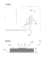
- a bowtie antenna 100 with a ground plane for its feed structure 105, 110 can be fabricated from a sheet of conductive material, prior to mounting on a wearable fabric.
- the antenna 100 as shown will be mounted on the inside of the wearable fabric and comprises a low-band bow-tie antenna 100 connected to the ground plane 110 of a transmission line feed via the ground plane 105 of a Marchand balun.
- the antenna and its feed structure share a continuous ground plane in that the ground plane of each is constructed from the same, continuous piece of material.
- balun is further discussed below with reference to Figures 5 and 6 .
- the antenna 100 is of known type, being a bow-tie dipole.
- the ground plane of the transmission line feed 110 is perforated and provides part of a 50 ohm microstrip line which is further described below with particular reference to Figures 2 to 4 .
- the microstrip line, and therefore the ground plane 110 is taken round a 90° bend to meet the ground plane 110 of the balun 105.
- Figure 1 also shows strips 115 joining the antenna 100 to the ground plane of the transmission line feed 110 and joining parts of the ground plane 105 of the Marchand balun but these strips 115 are only to aid positioning when attaching the antenna and feed structure to the wearable fabric and would be removed from the finished product.
- a transmission line feed 215 suitable for use in embodiments of the invention, which can be constructed using conductive fabrics, are:
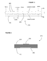
- the transmission line feed 215 of Figure 2 is provided by a conductor 200 having width "w” and a ground plane 210, on opposite sides of the wearable fabric 205 which has thickness "h".
- the nature of the wearable fabric 205 is not particularly critical. Embodiments of the transmission line feed 215 could be functional on at least most common clothing fabrics.
- the thickness "h" of the fabric 205 is not critical in the functioning of the transmission line feed 215 but an advantage of embodiments of the transmission line feed 215 is that they remain robust even when designed for fabrics 205 of no more than 1mm thickness. Indeed, they remain robust for use on clothes such as tee-shirts where the fabric 205 would commonly be no more than 0.5mm.
- the material of the transmission line feed 215 may be of any suitable conductive material and for experimental purposes might be for example copper tape.
- a suitable conductive material for use with wearable fabrics is Nora Dell Nickel-Copper-Silver plated nylon plain weave fabric, manufactured by Shieldex Trading Incorporated, with a quoted average resistivity of 0.005 ⁇ /sq.
- the antenna 100 and the ground plane 105, 110 of the balun and the transmission line feed 215 can be laser cut from this material.
- a working embodiment of the invention can be constructed using adhesive TESA ® tape (manufactured by TESA SE) applied to one side of the laser cut Nora Dell material. The backing is removed from the TESA tape and the design can be pressed on to the wearable fabric 205.
- adhesive TESA ® tape manufactured by TESA SE
- a transmission line 215 of this kind will be affected by the proximity of the ground plane 110 to the body in use, and will also lose a little power due to induced currents in the body. However, these effects can be kept relatively small if the period of the openings 300 is much smaller than the carrier wavelength in the wearable fabric 205, for instance by a factor of five or even ten or more.
- the width of the conductor can be kept in a range which is practical to use and for which the line will remain relatively undamaged due to flexing of the wearable fabric. In this way, lines with impedances of -50 ohms and below may be realised with conductor widths typically in the range 2-10mm.
- a cross section of the transmission line 215 shown in Figure 3 shows the structure as similar to that of the conventional microstrip transmission line on a cloth substrate shown in Figure 2 , but having a perforated ground plane 110
- the line 215 was 300mm long and terminated in a parallel pair of 100 ⁇ , surface-mounted resistors.
- the line conductor 200 was 3mm wide. Rectangular openings 300 having dimensions 8mm long x 4mm wide were made in the ground plane 110, spaced by 2mm conducting sections, reducing the capacitance per unit length by a factor of approximately 5. Because the capacitance was reduced, the velocity factor of the line 215 was close to 1.0.
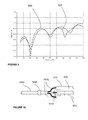
- the return loss of the terminated line 215 shown in Figure 3 was measured when the line 215 was isolated and when the grounded side of the line was placed against the body, producing two curves 505, 500 respectively.
- the capacitance introduced by the presence of the body was relatively small.
- This realisation of the feed line 215 with a punctured ground plane 110 is significantly easier to fabricate than one having dimensions as low as 0.8mm.
- the apertures 300 in the ground plane 110 are rectangular and periodic, providing a ladder-like structure. Neither of these characteristics is likely to be essential.
- the apertures 300 might instead be circular, of varying size and/or irregularly spaced. However, they are preferably at least as wide as the line conductor 200 so as to have maximum effect in reducing the amount of ground plane 110 under the conductor 200 per unit length.
- An important factor is the ratio of material present in the ground plane 110 under the conductor 200 to the openings. In a periodic structure, this might be seen as the duty ratio of the ground plane 110.
- this ratio of material could range widely, depending on the thickness and dielectric constant of the material. For any particular material there should be some ratio which gives an impedance of 50 ohms. The ratio would therefore have to be determined in practice in light of the material used.
- a suitable balun 600 to connect the transmission line 215 to the antenna 100 is of known type, being a planar Marchand balun based on a pair of Lange couplers 605A, 605B and 610A, 610B.
- Such a balun is described in the paper " Novel miniaturised wideband baluns for MIC and MMIC applications" by Nguyen and Smith, in Electronics Letters, Volume 29, No. 12, published on 10th June 1993 .
- the Marchand balun 600 consists of two parallel line couplers 605A, 605B and 610A, 610B, with one side of each coupler 605A, 610A connected to the ground plane 110 of the incoming transmission line 215.
- the other two lines 605B, 610B of the couplers are on the opposite side of the wearable fabric 205 (not shown in Figures 6 and 7 ) in use, being connected to the line conductor 200.
- the balun 600 also acts as a 4:1 impedance transformer, with an output of 200 ohms.
- the layout and dimensions of the Marchand balun 600 as described above are particularly convenient for direct coupling to a dipole antenna as well as to a transmission line 215 as described above with reference to Figures 2 to 4 .
- FIG 8 a cross section of the balun 600 shown in Figure 7 , using both sides of the wearable fabric 215, shows that overlapped coupled lines 605A, 605B and 610A, 610B are possible.
- the optimum coupling value for the couplers is 6.99dB when the balun 600 has a 4:1 ratio between the output and input impedances.
- a prototype balun 600 was constructed using copper tape as the coupled lines 605, 610 placed on both sides of a 0.2mm polyester substrate.
- the estimated dielectric constant of polyester film is approximately 3.2, similar to that of cotton fabric substrate 205, so that structures on the film have dimensions similar to those on the textile.
- the prototype balun 600 was 200mm long by 25mm wide, with 5mm wide tracks. To realise the correct coupling value, the tracks were separated by -0.2mm.
- the balun 600 was terminated in a 200 ohm resistor and connected to a 50 ohm flexible coaxial cable. The centre conductor of the coaxial cable was soldered to one of the inner lines and the outer was soldered to the point where the outer lines are connected to form a quarter-wave stub.
- the measured return loss of this balun 600 is shown in Figure 9 .
- the return loss was measured when the ground plane 605 of the balun 600 was isolated and when it was placed against the body, producing two curves 905, 900 respectively. (The effect of the body is variable and only one case is shown.) In isolation, the balun 600 has a reasonable return loss from 200-500MHz. The upper end of the frequency band is reduced by the proximity of the body.
- a bowtie antenna 100 fed with a Marchand balun 600 as described above was modelled. With the antenna 100 in vacuum, the real part of the complex impedance at the input to a nominal 50 ohm line oscillated around approximately 50 ohms across the 100-500 MHz band. The return loss indicated reasonable radiation efficiency from 100-500 MHz.
- a transmission line 215 will generally need to be connected to a radio in use. This can be done for example by using a length of coaxial cable 1000 connected to the TNC ("threaded Neill-Concelman") plug of the radio.
- the free end is held to the wearable fabric 205 (not shown in Figure 10 ) by using a clip or plastic tie 1005 such as Tywrap ® and the outer braid divided into two parts 1010 and attached to the ground plane 210 of the transmission line using a conductive epoxy resin such as silver-filled Araldite ® .
- the inner conductor 1015 is similarly attached to the line conductor 200 of the transmission line.
- Embodiments of the invention are suitable for use at radio frequencies, for example together with Multiband Inter/Intra Team Radios ("MBITRs").
- MBITRs Multiband Inter/Intra Team Radios
Landscapes
- Details Of Aerials (AREA)
Abstract
A feed structure for a wearable antenna incorporates a microstrip transmission line designed for mounting on opposite sides of a fabric. The transmission line has a perforated ground plane which reduces capacitance and offers an appropriate impedance, even when the fabric is thin, and allows the use of a relatively robust line conductor having a width of 3mm or 5mm or more. The ground plane can be extended to provide the ground plane of a balun and the material of that ground plane can in turn be extended to provide the wearable antenna.
Description
- The present invention relates to a feed structure for an antenna. Embodiments of the invention find particular application in flexible feed structures for radio antennas, such as those which can be incorporated into clothing.
- Wearable antennas have been developed for use in variety of communications applications. The construction of an antenna using flexible materials has been investigated and can give a relatively discreet result which does not hinder the wearer's movements.
- There are several challenges in developing a wearable antenna which can for example be incorporated into clothing. One of these is the feed for delivering communications signals to/from the antenna, these normally being at radio frequencies. The feed itself needs to deliver sufficient power while being relatively undetectable and also robust, for instance to withstand normal movement and handling of the clothing, and washing.
- A dipole antenna is a form of antenna known for use in a wearable construction but, in practice, it requires a balanced feed in order to prevent the feed itself from radiating as well as the antenna. If the feed radiates, it reduces the efficiency of the antenna, can distort the radiation/reception pattern and can interfere with other equipment. The output of a radio for use with a wearable communications antenna is unbalanced. It is known to use a transmission line plus a balun to convert the radio output to a balanced antenna feed.
- Other constraints with regard to an antenna feed suitable for wearable antennas are that it should be compatible with broadband operation and deliver an adequate signal power for use in the field, for example 5 Watts or more.
- According to a first aspect of the present invention, there is provided an antenna feed structure for use with a wearable antenna, the feed structure comprising a microstrip line having a line conductor and a ground plane for mounting on opposite sides of a flexible material, the ground plane having a series of apertures therein, at least partially facing the line conductor when mounted.
- Such a microstrip line might be connected to a balun to provide a balanced feed to a planar antenna.
- Typical, wearable cloth substrates, such as cotton, are often no more than 1 mm thick and can be no more than 0.5mm or 0.3mm. It has been found that, in a microstrip line of conventional design, having a line conductor and a continuous ground plane on opposite sides of a typical, wearable cloth substrate, the conductor has to be very narrow in order to achieve an impedance suitable for use with a communications radio. For example, if the radio has a 50 ohm input/output impedance and the cloth substrate is 0.3mm thick, the width of the line conductor has to be of the order of 0.8mm in order to match that impedance. Such narrow conductors are very difficult to realise and fragile in use.
- Embodiments of the invention allow a significantly wider conductor to be used to achieve the same impedance by reducing the capacitance of the microstrip line per unit length. A simple means of doing this is to remove sections of the ground plane below the line conductor, thereby reducing the amount of material in the ground plane per unit length.
- In use, the line conductor will be affected by the proximity of the ground plane to the body, and will also lose a fraction of the power by induced currents in the body. However, these effects can be kept relatively small as long as the spacing of the removed sections is kept small relative to the signal carrier wavelength. For example, it would be preferable to have five or more, or even ten or more, removed sections per carrier wavelength in the material. This effectively presents a reduced averaged capacitance in the transmission line and avoids problems with matching the line to an antenna.
- In embodiments of the invention, although not essential, the apertures in the ground plane might be periodic. For example, they might be provided by circular or rectangular openings providing a ladder-like structure. These openings are preferably at least as wide as the line conductor so as to have maximum effect in reducing the amount of ground plane per unit length. An important factor will therefore be the "duty ratio" of the periodic structure in the ground plane.
- According to a second aspect of the present invention, there is provided a wearable antenna assembly comprising a dipole antenna and an antenna feed structure, the assembly being carried at least partially on opposite sides of wearable fabric, and the antenna and feed structure having ground planes constructed from a shared, continuous piece of material. The wearable antenna assembly may comprise an antenna feed structure according to an embodiment of the invention in its first aspect, the feed structure being supported on opposite sides of flexible material having a thickness of not more than 1 mm.
- It has been found possible to construct an embodiment of the invention on materials no thicker than 0.5mm and even on cotton having a thickness of only 0.3mm. A conventional transmission line feed for an antenna would normally present considerable problems at these separations between the ground plane and the line conductor, particularly in terms of fragility, to achieve appropriate impedance. The perforated ground plane allows a wider line conductor to be used to achieve impedance in a convenient range, preferably around 50 ohms but optionally in the range from 35 ohms to 65 ohms, and this in turn means lower resistance and therefore lower loss.
- Rather than printing or otherwise providing the components of the transmission line directly onto a wearable material, it may be preferred to construct the components separately and then attach them to the wearable material. For example, the transmission line components might be constructed out of a metallised carrier such as a metallised fabric. A practical option is laser-cut, metallised nylon which offers quite high precision without adding thickness or stiffness to the wearable material.
- Embodiments of the invention allow a suitable antenna feed structure to be provided to communicate signals in a preferred frequency range of approximately 50-500MHz in spite of the tight requirements of wearable antennas in terms of detectability, robustness and electrical parameters.
- An antenna feed structure will now be described as an embodiment of the invention, by way of example only, with reference to the following figures in which:
-
Figure 1 shows a diagrammatic view from below of a bowtie antenna having a feed structure comprising an embodiment of the invention, during construction; -
Figure 2 shows a vertical cross section through a conventional microstrip feed line for an antenna; -
Figure 3 shows a diagrammatic view from above of the line conductor and ground plane of a microstrip feed line according to an embodiment of the invention; -
Figure 4 shows a cross section of the microstrip feed line ofFigure 3 , taken along the line A ― A and viewed in the direction indicated by the arrows; -
Figure 5 shows a graph of the measured return loss of a transmission line according toFigures 3 and 4 , 300mm long and terminated at a 50 ohm load; -
Figure 6 shows a diagrammatic plan view of the main elements of a planar Marchand balun; -
Figure 7 shows a diagrammatic plan view of a planar Marchand balun for use in the feed structure ofFigure 1 ; -
Figure 8 shows a cross section of the balun ofFigure 7 , taken along the line B ― B and viewed in the direction indicated by the arrows; -
Figure 9 shows a graph of the measured return loss of a balun according toFigures 7 and8 ; and -
Figure 10 shows a plan view of an arrangement for connecting the transmission line ofFigures 3 and 4 to a radio. - Referring to
Figure 1 , in practice, abowtie antenna 100 with a ground plane for itsfeed structure antenna 100 as shown will be mounted on the inside of the wearable fabric and comprises a low-band bow-tie antenna 100 connected to theground plane 110 of a transmission line feed via theground plane 105 of a Marchand balun. Thus in this embodiment the antenna and its feed structure share a continuous ground plane in that the ground plane of each is constructed from the same, continuous piece of material. - A suitable balun is further discussed below with reference to
Figures 5 and6 . - The
antenna 100 is of known type, being a bow-tie dipole. - The ground plane of the
transmission line feed 110 is perforated and provides part of a 50 ohm microstrip line which is further described below with particular reference toFigures 2 to 4 . To obtain vertical polarisation, the microstrip line, and therefore theground plane 110, is taken round a 90° bend to meet theground plane 110 of thebalun 105. -
Figure 1 also showsstrips 115 joining theantenna 100 to the ground plane of thetransmission line feed 110 and joining parts of theground plane 105 of the Marchand balun but thesestrips 115 are only to aid positioning when attaching the antenna and feed structure to the wearable fabric and would be removed from the finished product. - Referring to
Figure 2 , important aspects of atransmission line feed 215 suitable for use in embodiments of the invention, which can be constructed using conductive fabrics, are: - ● power handling of the conducting fabric when used as a transmission line
- ● effect on impedance due to coupling into the body, in use
- ● thickness achievable across typical wearable fabrics
- The
transmission line feed 215 ofFigure 2 is provided by aconductor 200 having width "w" and aground plane 210, on opposite sides of thewearable fabric 205 which has thickness "h". - The nature of the
wearable fabric 205 is not particularly critical. Embodiments of thetransmission line feed 215 could be functional on at least most common clothing fabrics. The thickness "h" of thefabric 205 is not critical in the functioning of thetransmission line feed 215 but an advantage of embodiments of thetransmission line feed 215 is that they remain robust even when designed forfabrics 205 of no more than 1mm thickness. Indeed, they remain robust for use on clothes such as tee-shirts where thefabric 205 would commonly be no more than 0.5mm. - The material of the
transmission line feed 215 may be of any suitable conductive material and for experimental purposes might be for example copper tape. However, a suitable conductive material for use with wearable fabrics is Nora Dell Nickel-Copper-Silver plated nylon plain weave fabric, manufactured by Shieldex Trading Incorporated, with a quoted average resistivity of 0.005 Ω/sq. Theantenna 100 and theground plane transmission line feed 215 can be laser cut from this material. - Although other attachment techniques might be desirable in practice, a working embodiment of the invention can be constructed using adhesive TESA® tape (manufactured by TESA SE) applied to one side of the laser cut Nora Dell material. The backing is removed from the TESA tape and the design can be pressed on to the
wearable fabric 205. - Referring to
Figure 3 , using a conventional microstrip transmission line on a cloth substrate such as thewearable fabric 205 described above, with thickness -0.3mm, would mean that the widths of the transmission lines would have to be inconveniently small. For example, a 50 ohm track on cotton would have to be roughly 0.8mm wide. Such athin conducting line 200 is difficult to realise using metallised fabric as a thin strip of material will have a higher effective resistivity and will be prone to fray. - Wider tracks are possible however if the effective capacitance per unit length can be reduced. In embodiments of the invention, sections of the
ground plane 110 below the conductingline 200 are removed to formopenings 300. Atransmission line 215 of this kind will be affected by the proximity of theground plane 110 to the body in use, and will also lose a little power due to induced currents in the body. However, these effects can be kept relatively small if the period of theopenings 300 is much smaller than the carrier wavelength in thewearable fabric 205, for instance by a factor of five or even ten or more. - Using this method, the width of the conductor can be kept in a range which is practical to use and for which the line will remain relatively undamaged due to flexing of the wearable fabric. In this way, lines with impedances of -50 ohms and below may be realised with conductor widths typically in the range 2-10mm.
- Referring to
Figure 4 , a cross section of thetransmission line 215 shown inFigure 3 , through one of theopenings 300, shows the structure as similar to that of the conventional microstrip transmission line on a cloth substrate shown inFigure 2 , but having aperforated ground plane 110 - Referring to
Figure 5 , copper tape and the cotton fabric described above were used to construct a prototype of thetransmission line 215 shown inFigure 3 , for testing purposes. Theline 215 was 300mm long and terminated in a parallel pair of 100Ω, surface-mounted resistors. Theline conductor 200 was 3mm wide.Rectangular openings 300 having dimensions 8mm long x 4mm wide were made in theground plane 110, spaced by 2mm conducting sections, reducing the capacitance per unit length by a factor of approximately 5. Because the capacitance was reduced, the velocity factor of theline 215 was close to 1.0. - The return loss of the terminated
line 215 shown inFigure 3 was measured when theline 215 was isolated and when the grounded side of the line was placed against the body, producing twocurves - This realisation of the
feed line 215 with a puncturedground plane 110 is significantly easier to fabricate than one having dimensions as low as 0.8mm. - As shown in
Figures 3 and 4 , theapertures 300 in theground plane 110 are rectangular and periodic, providing a ladder-like structure. Neither of these characteristics is likely to be essential. For example, theapertures 300 might instead be circular, of varying size and/or irregularly spaced. However, they are preferably at least as wide as theline conductor 200 so as to have maximum effect in reducing the amount ofground plane 110 under theconductor 200 per unit length. An important factor is the ratio of material present in theground plane 110 under theconductor 200 to the openings. In a periodic structure, this might be seen as the duty ratio of theground plane 110. However, this ratio of material could range widely, depending on the thickness and dielectric constant of the material. For any particular material there should be some ratio which gives an impedance of 50 ohms. The ratio would therefore have to be determined in practice in light of the material used. - Referring to
Figures 6 and 7 , in a completed feed assembly for thebowtie antenna 100 ofFigure 1 , asuitable balun 600 to connect thetransmission line 215 to theantenna 100 is of known type, being a planar Marchand balun based on a pair of Lange couplers 605A, 605B and 610A, 610B. Such a balun is described in the paper "Novel miniaturised wideband baluns for MIC and MMIC applications" by Nguyen and Smith, in Electronics Letters, Volume 29, No. 12, published on 10th June 1993. - The Marchand balun 600 consists of two
parallel line couplers coupler ground plane 110 of theincoming transmission line 215. The other twolines Figures 6 and 7 ) in use, being connected to theline conductor 200. Thebalun 600 also acts as a 4:1 impedance transformer, with an output of 200 ohms. - The layout and dimensions of the
Marchand balun 600 as described above are particularly convenient for direct coupling to a dipole antenna as well as to atransmission line 215 as described above with reference toFigures 2 to 4 . - Referring to
Figure 8 , a cross section of thebalun 600 shown inFigure 7 , using both sides of thewearable fabric 215, shows that overlapped coupledlines balun 600 has a 4:1 ratio between the output and input impedances. - A
prototype balun 600 was constructed using copper tape as the coupled lines 605, 610 placed on both sides of a 0.2mm polyester substrate. The estimated dielectric constant of polyester film is approximately 3.2, similar to that ofcotton fabric substrate 205, so that structures on the film have dimensions similar to those on the textile. Theprototype balun 600 was 200mm long by 25mm wide, with 5mm wide tracks. To realise the correct coupling value, the tracks were separated by -0.2mm. Thebalun 600 was terminated in a 200 ohm resistor and connected to a 50 ohm flexible coaxial cable. The centre conductor of the coaxial cable was soldered to one of the inner lines and the outer was soldered to the point where the outer lines are connected to form a quarter-wave stub. - The measured return loss of this
balun 600 is shown inFigure 9 . The return loss was measured when the ground plane 605 of thebalun 600 was isolated and when it was placed against the body, producing twocurves balun 600 has a reasonable return loss from 200-500MHz. The upper end of the frequency band is reduced by the proximity of the body. - A
bowtie antenna 100 fed with aMarchand balun 600 as described above was modelled. With theantenna 100 in vacuum, the real part of the complex impedance at the input to a nominal 50 ohm line oscillated around approximately 50 ohms across the 100-500 MHz band. The return loss indicated reasonable radiation efficiency from 100-500 MHz. - Referring to
Figure 10 , atransmission line 215 according to an embodiment of the invention will generally need to be connected to a radio in use. This can be done for example by using a length ofcoaxial cable 1000 connected to the TNC ("threaded Neill-Concelman") plug of the radio. The free end is held to the wearable fabric 205 (not shown inFigure 10 ) by using a clip orplastic tie 1005 such as Tywrap® and the outer braid divided into twoparts 1010 and attached to theground plane 210 of the transmission line using a conductive epoxy resin such as silver-filled Araldite®. Theinner conductor 1015 is similarly attached to theline conductor 200 of the transmission line. - Embodiments of the invention are suitable for use at radio frequencies, for example together with Multiband Inter/Intra Team Radios ("MBITRs").
Claims (15)
- An antenna feed structure for use with a wearable antenna, the feed structure comprising a microstrip transmission line having a line conductor and a ground plane for mounting on opposite sides of a flexible material, the ground plane having a series of apertures therein, at least partially facing the line conductor when the microstrip transmission line is mounted on the flexible material.
- An antenna feed structure according to Claim 1 wherein at least some of the apertures are at least as wide as the line conductor.
- An antenna feed structure according to Claim 2 wherein all of the apertures are at least as wide as the line conductor.
- An antenna feed structure according to any one of Claims 1 to 3 wherein the line conductor extends centrally with respect to the apertures when the microstrip transmission line is mounted on the flexible material.
- An antenna feed structure according to any one of the preceding claims wherein the distribution of the apertures has a periodicity along the length of the transmission line which is greater than the carrier wavelength of signals to be carried in use of the transmission line.
- An antenna feed structure according to any one of the preceding claims wherein the distribution of the apertures has a periodicity along the length of the transmission line which is at least four times that of the carrier wavelength of signals to be carried in use of the transmission line.
- An antenna feed structure according to any one of the preceding claims wherein the distribution of the apertures has a periodicity along the length of the transmission line which is at least ten times that of the carrier wavelength of signals to be carried in use of the transmission line.
- An antenna feed structure according to any one of the preceding claims wherein the dimensions of the apertures are such that they present at least half of the ground plane facing the line conductor when the microstrip transmission line is mounted on the flexible material.
- An antenna feed structure according to any one of the preceding claims wherein the dimensions of the apertures are such that they present at least sixty per cent of the ground plane facing the line conductor when the microstrip transmission line is mounted on the flexible material.
- An antenna feed structure according to any one of the preceding claims wherein the material of the ground plane of the transmission line is extended beyond the line conductor to provide a ground plane for a balun.
- An antenna feed structure according to Claim 5 wherein the material of the ground plane of the balun is extended to provide the antenna.
- An antenna feed structure according to any one of the preceding claims wherein the microstrip transmission line has an impedance, in use, in the range 35 to 65 ohms.
- An antenna feed structure according to any one of the preceding claims wherein the line conductor has a width in the range 2 mm to 10 mm.
- An antenna feed structure according to any one of the preceding claims wherein the microstrip transmission line is constructed out of metallised fabric.
- A wearable antenna assembly comprising an antenna feed structure according to any one of Claims 1 to 14.
Priority Applications (4)
| Application Number | Priority Date | Filing Date | Title |
|---|---|---|---|
| EP10275069A EP2403063A1 (en) | 2010-06-30 | 2010-06-30 | Antenna Feed Structure |
| EP11731039.1A EP2589106B1 (en) | 2010-06-30 | 2011-06-29 | Antenna feed structure |
| PCT/GB2011/000994 WO2012001367A1 (en) | 2010-06-30 | 2011-06-29 | Antenna feed structure |
| US13/702,348 US9118096B2 (en) | 2010-06-30 | 2011-06-29 | Wearable antenna having a microstrip feed line disposed on a flexible fabric and including periodic apertures in a ground plane |
Applications Claiming Priority (1)
| Application Number | Priority Date | Filing Date | Title |
|---|---|---|---|
| EP10275069A EP2403063A1 (en) | 2010-06-30 | 2010-06-30 | Antenna Feed Structure |
Publications (1)
| Publication Number | Publication Date |
|---|---|
| EP2403063A1 true EP2403063A1 (en) | 2012-01-04 |
Family
ID=42752366
Family Applications (1)
| Application Number | Title | Priority Date | Filing Date |
|---|---|---|---|
| EP10275069A Ceased EP2403063A1 (en) | 2010-06-30 | 2010-06-30 | Antenna Feed Structure |
Country Status (1)
| Country | Link |
|---|---|
| EP (1) | EP2403063A1 (en) |
Cited By (2)
| Publication number | Priority date | Publication date | Assignee | Title |
|---|---|---|---|---|
| US9281172B2 (en) | 2005-12-07 | 2016-03-08 | Micromass Uk Limited | Closed loop ion guide with pseudo-potential well |
| US20240266756A1 (en) * | 2021-07-29 | 2024-08-08 | Lg Electronics Inc. | Electronic device having antenna |
Citations (4)
| Publication number | Priority date | Publication date | Assignee | Title |
|---|---|---|---|---|
| WO1998016966A1 (en) * | 1996-10-11 | 1998-04-23 | Avnet, Inc. | Broad band dipole element and array |
| US20020084876A1 (en) * | 2000-12-29 | 2002-07-04 | Wright Mitchel E. | Slotted ground plane for controlling the impedance of high speed signals on a printed circuit board |
| US20060119525A1 (en) * | 2004-08-24 | 2006-06-08 | Nathan Cohen | Wideband antenna system for garments |
| WO2009030039A1 (en) * | 2007-09-04 | 2009-03-12 | Sierra Wireless, Inc. | Antenna configurations for compact device wireless communication |
-
2010
- 2010-06-30 EP EP10275069A patent/EP2403063A1/en not_active Ceased
Patent Citations (4)
| Publication number | Priority date | Publication date | Assignee | Title |
|---|---|---|---|---|
| WO1998016966A1 (en) * | 1996-10-11 | 1998-04-23 | Avnet, Inc. | Broad band dipole element and array |
| US20020084876A1 (en) * | 2000-12-29 | 2002-07-04 | Wright Mitchel E. | Slotted ground plane for controlling the impedance of high speed signals on a printed circuit board |
| US20060119525A1 (en) * | 2004-08-24 | 2006-06-08 | Nathan Cohen | Wideband antenna system for garments |
| WO2009030039A1 (en) * | 2007-09-04 | 2009-03-12 | Sierra Wireless, Inc. | Antenna configurations for compact device wireless communication |
Non-Patent Citations (1)
| Title |
|---|
| NGUYEN; SMITH: "Novel miniaturised wideband baluns for MIC and MMIC applications", ELECTRONICS LETTERS, vol. 29, no. 12, 10 June 1993 (1993-06-10) |
Cited By (3)
| Publication number | Priority date | Publication date | Assignee | Title |
|---|---|---|---|---|
| US9281172B2 (en) | 2005-12-07 | 2016-03-08 | Micromass Uk Limited | Closed loop ion guide with pseudo-potential well |
| US20240266756A1 (en) * | 2021-07-29 | 2024-08-08 | Lg Electronics Inc. | Electronic device having antenna |
| US12261369B2 (en) * | 2021-07-29 | 2025-03-25 | Lg Electronics Inc. | Electronic device having antenna |
Similar Documents
| Publication | Publication Date | Title |
|---|---|---|
| EP2589106B1 (en) | Antenna feed structure | |
| KR100955801B1 (en) | Multiband Internal Antenna | |
| EP2940795B1 (en) | Multiband antenna | |
| US7116274B2 (en) | Planar inverted F antenna | |
| CN106068580B (en) | Dual Band Printed Omnidirectional Antenna | |
| CN106299673B (en) | A kind of small sized wide-band circular polarized antenna | |
| US20050110680A1 (en) | Microstrip antenna | |
| KR20160144920A (en) | Dipole antenna with integrated balun | |
| JP2009194832A (en) | Wideband antenna, and wear or property employing the same | |
| CN101542841A (en) | Dual polarization wave antenna | |
| US20100277389A1 (en) | Compact circular polarized antenna | |
| KR102718243B1 (en) | Multi band antenna module | |
| US10992047B2 (en) | Compact folded dipole antenna with multiple frequency bands | |
| US9024840B2 (en) | Antenna structure | |
| EP2403062A1 (en) | Antenna structure | |
| CN204243180U (en) | A Circularly Polarized Antenna with Horizontal Omnidirectional Radiation | |
| US8912965B2 (en) | Substrate antenna | |
| Liu et al. | A patch array antenna for 60 GHz package applications | |
| CN105742792A (en) | Circular polarized antenna capable of realizing horizontal all-direction radiation | |
| CN211126059U (en) | Dual-band antenna and aircraft | |
| TW201218506A (en) | Antenna having planar conducting elements, one of which has a slot | |
| JP2001168632A (en) | Horn antenna and primary radiator | |
| CN115810896A (en) | Microstrip Antennas and Positioning Systems | |
| WO2021078200A1 (en) | Dual-frequency antenna and aerial vehicle | |
| CN112490640A (en) | Broadband electromagnetic dipole circularly polarized antenna |
Legal Events
| Date | Code | Title | Description |
|---|---|---|---|
| AK | Designated contracting states |
Kind code of ref document: A1 Designated state(s): AL AT BE BG CH CY CZ DE DK EE ES FI FR GB GR HR HU IE IS IT LI LT LU LV MC MK MT NL NO PL PT RO SE SI SK SM TR |
|
| AX | Request for extension of the european patent |
Extension state: BA ME RS |
|
| PUAI | Public reference made under article 153(3) epc to a published international application that has entered the european phase |
Free format text: ORIGINAL CODE: 0009012 |
|
| STAA | Information on the status of an ep patent application or granted ep patent |
Free format text: STATUS: THE APPLICATION HAS BEEN REFUSED |
|
| 18R | Application refused |
Effective date: 20120127 |