EP2403030A2 - Organic light emitting diode display - Google Patents
Organic light emitting diode display Download PDFInfo
- Publication number
- EP2403030A2 EP2403030A2 EP11171668A EP11171668A EP2403030A2 EP 2403030 A2 EP2403030 A2 EP 2403030A2 EP 11171668 A EP11171668 A EP 11171668A EP 11171668 A EP11171668 A EP 11171668A EP 2403030 A2 EP2403030 A2 EP 2403030A2
- Authority
- EP
- European Patent Office
- Prior art keywords
- light emitting
- layer
- emitting region
- organic
- emitting diode
- Prior art date
- Legal status (The legal status is an assumption and is not a legal conclusion. Google has not performed a legal analysis and makes no representation as to the accuracy of the status listed.)
- Ceased
Links
Images


Classifications
-
- H—ELECTRICITY
- H10—SEMICONDUCTOR DEVICES; ELECTRIC SOLID-STATE DEVICES NOT OTHERWISE PROVIDED FOR
- H10K—ORGANIC ELECTRIC SOLID-STATE DEVICES
- H10K59/00—Integrated devices, or assemblies of multiple devices, comprising at least one organic light-emitting element covered by group H10K50/00
- H10K59/30—Devices specially adapted for multicolour light emission
- H10K59/35—Devices specially adapted for multicolour light emission comprising red-green-blue [RGB] subpixels
-
- H—ELECTRICITY
- H10—SEMICONDUCTOR DEVICES; ELECTRIC SOLID-STATE DEVICES NOT OTHERWISE PROVIDED FOR
- H10K—ORGANIC ELECTRIC SOLID-STATE DEVICES
- H10K50/00—Organic light-emitting devices
- H10K50/80—Constructional details
- H10K50/805—Electrodes
- H10K50/82—Cathodes
- H10K50/828—Transparent cathodes, e.g. comprising thin metal layers
-
- H—ELECTRICITY
- H10—SEMICONDUCTOR DEVICES; ELECTRIC SOLID-STATE DEVICES NOT OTHERWISE PROVIDED FOR
- H10K—ORGANIC ELECTRIC SOLID-STATE DEVICES
- H10K50/00—Organic light-emitting devices
- H10K50/80—Constructional details
- H10K50/805—Electrodes
-
- H—ELECTRICITY
- H10—SEMICONDUCTOR DEVICES; ELECTRIC SOLID-STATE DEVICES NOT OTHERWISE PROVIDED FOR
- H10K—ORGANIC ELECTRIC SOLID-STATE DEVICES
- H10K50/00—Organic light-emitting devices
- H10K50/80—Constructional details
- H10K50/805—Electrodes
- H10K50/81—Anodes
- H10K50/816—Multilayers, e.g. transparent multilayers
-
- H—ELECTRICITY
- H10—SEMICONDUCTOR DEVICES; ELECTRIC SOLID-STATE DEVICES NOT OTHERWISE PROVIDED FOR
- H10K—ORGANIC ELECTRIC SOLID-STATE DEVICES
- H10K50/00—Organic light-emitting devices
- H10K50/80—Constructional details
- H10K50/85—Arrangements for extracting light from the devices
- H10K50/852—Arrangements for extracting light from the devices comprising a resonant cavity structure, e.g. Bragg reflector pair
-
- H—ELECTRICITY
- H10—SEMICONDUCTOR DEVICES; ELECTRIC SOLID-STATE DEVICES NOT OTHERWISE PROVIDED FOR
- H10K—ORGANIC ELECTRIC SOLID-STATE DEVICES
- H10K59/00—Integrated devices, or assemblies of multiple devices, comprising at least one organic light-emitting element covered by group H10K50/00
- H10K59/80—Constructional details
- H10K59/805—Electrodes
Definitions
- the described technology generally relates to an organic light emitting diode (OLED) display.
- OLED organic light emitting diode
- an electroluminescent device uses an electroluminescence (EL) phenomenon whereby light is generated when a predetermined electric field is applied to phosphor.
- EL devices are generally classified into inorganic or organic type according to the material used to form a light emitting layer. Since an organic EL device emits light across a broad colour spectrum and has desirable characteristics such as high luminance and low driving voltage, it has received considerable attention for commercial applications.
- a pixel area defined by a plurality of scan lines and a plurality of data lines formed in a direction substantially perpendicular thereto implements each of red, green, and blue sub-pixels, thereby making it possible to configure a matrix of pixels into a full-colour flat panel device.
- a first electrode layer having a predetermined pattern is formed on the upper portion of a substrate including a red pixel area, a green pixel area, and a blue pixel area in order to implement red (R), green (G), and blue (B), respectively.
- the organic layer including the light emitting layer is formed on the upper portion of the first electrode layer.
- the organic layer may include a hole injection layer (HIL), a hole transport layer (HTL), a hole blocking layer, an electron transport layer (ETL), and an electron injection layer (EIL) in addition to the light emitting layer.
- a second electrode layer is formed on the upper portion of the organic layer over the substrate.
- the organic layer may be formed by a deposition method, an ink jet method, a laser thermal induced method, or the like.
- One inventive aspect is an organic light emitting diode display capable of making substantially uniformly thick organic layers for blue, green and red light emitting regions, while implementing full colour.
- an organic light emitting diode display including: a plurality of pixels defined by a blue light emitting region, a green light emitting region, and a red light emitting region on a substrate and formed by stacking a lower electrode, an organic layer, and an upper electrode, wherein the blue and green light emitting regions are formed in a microcavity structure and the red light emitting region is formed in a non-microcavity structure.
- an organic light emitting diode display including: a substrate having a plurality of light emitting regions defined by a blue light emitting region, a green light emitting region, and a red light emitting region; a lower electrode formed in the blue and green light emitting regions, and formed by stacking a first transparent conductive layer, a semitransparent metal layer, and a second transparent conductive layer; and a lower electrode formed of a transparent conductive layer in the red light emitting region.
- OLED organic light emitting diode
- a plurality of pixels comprising a blue light emitting region, a green light emitting region, and a red light emitting region on a substrate and formed by stacking a lower electrode, an organic layer, and an upper electrode, wherein the lower electrode of the blue and green light emitting regions is formed of at least one transparent layer and at least one semitransparent layer and wherein the lower electrode of the red light emitting region is formed of only a transparent layer.
- the lower electrode of the red light emitting region is formed of one or more transparent conductive layers.
- the lower electrode of the blue and green light emitting regions is formed of a first transparent conductive layer, a semitransparent metal layer, and a second transparent conductive layer which are sequentially formed.
- the thickness of the first transparent conductive layer is from about 50 nm to about 150 nm and the thickness of the second transparent conductive layer is from about 10 nm to about 20 nm.
- the thickness of the semitransparent metal layer is from about 5 nm to about 20 nm. In the above display, the thickness of the organic layer is from about 50 nm to about 60 nm.
- the organic layers formed on the blue light emitting region, the green light emitting region, and the red light emitting region include a blue emission layer, a green emission layer, and a red emission layer, respectively.
- the organic layer further includes at least one of: a hole injection layer (HIL), a hole transport layer (HTL), a hole blocking layer and, an electron injection layer (EIL).
- HIL hole injection layer
- HTL hole transport layer
- EIL electron injection layer
- the thickness of the hole injection layer (HIL) and the hole transport layer (HTL) is from about 19 nm to about 36 nm.
- the thickness of the organic layer in the red light emitting region is substantially the same as the thickness of the red right emitting layer or is about 60 nm.
- the above display further comprises: a colour filter or a colour converting layer formed on the upper electrode of the red light emitting region.
- the above display further comprises: an encapsulation substrate bonded to the substrate and including the colour filter or a colour converting layer formed to correspond to the red light emitting region.
- OLED organic light emitting diode
- a substrate having a plurality of light emitting regions which comprise a blue light emitting region, a green light emitting region, and a red light emitting region; a first lower electrode formed in the blue and green light emitting regions, and formed by stacking a first transparent conductive layer, a semitransparent metal layer, and a second transparent conductive layer; and a second lower electrode formed in the red light emitting region and formed of only a transparent conductive layer.
- an organic layer and an upper electrode are further formed on the lower electrodes.
- the thickness of the first transparent conductive layer is from about 50 nm to about 150 nm and the thickness of the second transparent conductive layer is from about 10 nm to about 20 nm.
- the thickness of the semitransparent metal layer is from about 5 nm to about 20 nm.
- the thickness of the organic layer is from about 50 nm to about 60 nm.
- OLED organic light emitting diode
- a plurality of pixels each of which comprises blue, red and green sub-pixels configured to emit blue, red and green light, respectively; a first lower electrode formed in the blue and green sub-pixels, wherein the first lower electrode comprises at least one transparent layer and at least one semitransparent layer; and a second lower electrode formed in the red sub-pixel and formed of a transparent conductive layer, wherein the second lower electrode does not include a semitransparent layer.
- the first lower electrode comprises i) a first transparent conductive layer, ii) a semitransparent metal layer and iii) a second transparent conductive layer which are sequentially formed.
- the second lower electrode is formed of one or more transparent conductive layers.
- a first electrode having an ITO/Ag/ITO structure is used to transmit a portion of emitted light and resonate another portion of the emitted light.
- the thickness of the organic layer in the red area should be formed to be thicker than that of the organic layer in the blue and green areas in order to generate the desired degree of resonance. Therefore, the thickness of the organic layer formed in each light emitting region becomes non-uniform.
- an organic light emitting diode display according to an embodiment will be described more fully hereinafter with reference to the accompanying drawings.
- the disclosed embodiments mainly describe the case where a plurality of pixels defined by blue, green and red light emitting regions are formed on a substrate. Further, the disclosed embodiments describe, by way of example, an active matrix organic light emitting diode display; however, they may be applied to a passive matrix organic light emitting diode display.
- a buffer layer 210 is formed over a substrate 200 and an amorphous silicon layer is formed on the buffer layer 210 by, for example, a deposition method such as PECVD, LPCVD, or the like.
- the substrate 200 may be an insulating substrate such as glass, quartz, sapphire, etc., and the buffer layer 210 prevents the amorphous silicon layer from being polluted by impurities diffused from the substrate 200.
- the amorphous silicon layer may be crystallized by methods such as excimer laser annealing (ELA), sequential lateral solidification (SLS), metal induced crystallization (MIC) or metal induced lateral crystallization (MILC).
- ELA excimer laser annealing
- SLS sequential lateral solidification
- MIC metal induced crystallization
- MILC metal induced lateral crystallization
- the amorphous silicon layer may be patterned by a photolithography process to form a semiconductor layer 220 in a thin layer transistor area in a unit pixel.
- a gate insulating layer 230 is formed over the substrate 200 including the semiconductor layer 220.
- the gate insulating layer 230 may be formed at least partially of silicon oxide, silicon nitride or may be formed in a stacked structure thereof.
- the gate electrode 240 is formed to be partially overlapping with the semiconductor layer 220, and the semiconductor layer 220 area overlapping with the gate electrode 240 is defined as the channel area.
- the gate electrode 240 may be formed of a single layer of an aluminium alloy of aluminium (Al) or aluminium-neodymium (Al-Nd) or of a multi-layer in which aluminium alloy is stacked on chromium (Cr) or molybdenum (Mo) alloy.
- the interlayer insulating layer 250 may use a silicon nitride layer or a silicon oxide layer.
- a metal layer (not shown) is formed on an interlayer insulating layer 250 and is then patterned, thereby forming source/drain electrodes 260a and 260b.
- the source/drain electrodes 260a and 260b are electrically connected to the source area and the drain area of the semiconductor layer 220 through a contact hole formed by partially etching the gate insulating layer 230 and the interlayer insulating layer 250.
- the metal layer forms a single layer selected from a group of Mo, W, MoW, AlNd, Ti, Cu, Cu alloy, Al, Al alloy, Ag and Ag alloy, etc.
- the metal layer may be formed of one stacking structure selected from one group consisting of a two-layer structure of Mo, Cu, Al or Ag that is a low resistance material or a multilayer structure of two layers or more.
- the planarization layer 280 may be formed at least partially of polyimide, benzocyclobutene based resin, and acrylate.
- the protective layer 270 and the planarization layer 280 are partially etched to form a via hole that exposes any one of source/drain electrodes 260a and 260b and the lower electrode 290 formed on the planarization layer 280 is electrically connected to any one of the source/drain electrodes 260a and 260b exposed through a via hole.
- the lower electrode 290 is formed in a blue light emitting region (a), a green light emitting region (b), a red light emitting region (c), respectively, and the position in which the light emitting region is formed is not limited thereto.
- a pixel defining layer 295 having an opening is formed on the upper of the lower electrode 290 to expose a portion of the lower electrode 290 through the opening and to form the organic layer 300 on the lower electrode 290 that is opened.
- the pixel defining layer 295 may be formed at least partially of polyimide, benzocyclobutene series resin, spin-on glass (SOG), and acrylate.
- the upper electrode 310 is formed over the substrate 200 to complete the organic light emitting diode.
- the upper electrode 310 may be formed at least partially of Li, Ca, LiF/Ca, LiF/Al, Al, Mg and an alloy thereof.
- the lower electrode 290 formed in the blue light emitting region (a) is formed by sequentially stacking the first transparent conductive layer 290a, a semitransparent metal layer 290c, and the second transparent conductive layer 290b and the organic layer 300 is formed on the lower electrode 290.
- the lower electrode 290 of the blue light emitting region (a) may include at least one transparent conductive layer and at least one semitransparent metal layer. This applies to the lower electrode 290 formed in the green light emitting region (b).
- the first and second transparent conductive layers 290a and 290b may be formed at least partially of indium tin oxide (ITO), an indium zinc oxide (IZO), tin oxide (To), and zinc oxide (ZnO).
- the first transparent conductive layer 290a substantially serves as an anode and the second transparent conductive layer 290b serves to match work function, thereby completing the lower electrode 290.
- the first transparent conductive layer 290a has good light efficiency of blue, green, red within a thickness of about 50 nm to about 150 nm of blue, green, and red and thus, the first transparent conductive layer 290a is formed at the thickness of about 50 nm to about 150 nm.
- the second transparent conductive layer 290b is formed at about 10 nm or more to sufficiently perform a role of the anode and since it is considered together with the thickness of the organic layer, it may be formed at about 30 nm or less in order to maximize the microcavity (resonance) effect of light generated from the organic light emitting layer.
- the semitransparent metal layer 290c may be formed at least partially of Ag, Al, Ni, Pt and Pd. In one embodiment, the thickness of the semitransparent metal layer 290c is from about 5 nm to about 20 nm. This range may provide an optimum balance between light transmittance and the functionality as a metal electrode. However, the thickness of the semitransparent metal layer 290c may be less than about 5 nm or greater than about 20 nm.
- the organic layer 300 may further include at least one of the blue light emitting layer 303a, the hole injection layer 301 positioned between the blue light emitting layer 303a and the lower electrode 290 other than the blue light emitting layer 303a, the hole blocking layer 304 positioned on the hole transport layer 302 and the blue light emitting layer 303a and the electron injection layer 305.
- the organic layer 300 may be formed at the thickness of about 50 nm to about 60 nm in consideration of the light emitting luminance and the colour reproduction rate. Alternatively, the thickness of the organic layer 300 may be less than about 50 nm or greater than about 60 nm.
- the thickness of the hole injection layer 301 and the hole transport layer 302 between the lower electrode 290 and the blue light emitting layer 303a maximizes the luminance and the microcavity effect, such that they may be formed at a thickness of about 19 nm to about 36 nm in order to maximize the microcavity effect.
- the thickness of the layers 301 and 302 may be less than about 19 nm or greater than about 36 nm.
- the lower electrode 290 formed in the green light emitting region (b) is formed by sequentially stacking the first transparent conductive layer 290a, the semitransparent metal layer 290c and the second transparent conductive layer 290b and the organic layer 300 is formed on the lower electrode 290.
- the description for the layers 290a-290c and organic layer 300 of the blue light emitting region (a) applies to those of the green light emitting region (b), except that in FIG. 2B , the organic layer 300 includes a green light emitting layer 303b instead of the blue light emitting layer 303a.
- the lower electrode 290 formed in the red light emitting region (c) is formed of the transparent conductive layer and the organic layer 300 is formed on the lower electrode 290.
- the lower electrode 290 may be formed in a single layer or a multilayer structure of the transparent conductive layer.
- the transparent conductive layer may be formed at least partially of indium tin oxide (ITO), an indium zinc oxide (IZO), tin oxide (TO), and zinc oxide (ZnO) and serves as the anode of the lower electrode 290.
- the thickness of the lower electrode 290 is determined together with the thickness of the organic layer 300 in order to increase the light emitting luminance and the colour reproduction rate.
- the organic layer 300 includes the red light emitting layer 303c and may further include at least one of the hole injection layer 301 positioned between the lower electrode 290 and the red light emitting layer 303c, the hole blocking layer 304 positioned on the hole transport layer 302 and the red light emitting layer 303c and the electron injection layer 305.
- the organic layer 300 may be formed at the thickness of about 50 nm to about 60 nm in consideration of the light emitting luminance, the colour reproduction rate, the thickness of the organic layers of the blue light emitting region and the green light emitting region, etc.
- the red light emitting region can sufficiently satisfy the colour reproduction rate by including only the red light emitting layer and thus, may be formed at the thickness of the red light emitting layer to the thickness of about 60 nm, but is not limited thereto.
- the red light emitting layer is about 33.6 nm to about 35.6 nm, the light emitting efficiency and the colour reproduction rate is excellent.
- the lower electrode formed in the blue light emitting region and the green light emitting region has a structure of the first transparent conductive layer/semitransparent metal layer/second transparent conductive layer, but the lower electrode positioned in the red light emitting region is formed of the transparent conductive layer.
- a microcavity (resonance) structure is formed in the blue light emitting region and the green light emitting region, but a non-microcavity structure is formed in the red light emitting region.
- the red light emitting region does not include a microcavity/resonance structure.
- the thickness of the organic layer of the red light emitting region is thicker than the thickness of the organic layer of the blue light emitting region and the green light emitting region.
- the thickness of the organic layers of the blue light emitting region and the green light emitting region is uniform by controlling the thickness of the organic layer of the red light emitting region.
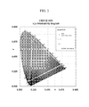
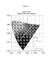
- FIGS. 3 and 4 are CIE-based colour coordinates for explaining a colour reproduction rate when the red light emitting region is formed in a non-microcavity structure, wherein FIG. 3 shows a colour coordinate system according to CIE 1931 colour space, also known as the CIE XYZ colour space and FIG. 4 shows a colour coordinate system according to CIE 1976 (L*, u*, v*) colour space, also known as CIELUV.
- Table 1 shows results obtained by comparing the colour coordinate, the colour reproduction area, and the colour reproduction rate with the NTSC when the red light emitting region is formed in the non-microcavity structure in the colour coordinate of FIG. 3 and the following Table 2 shows results obtained by comparing the colour coordinate, the colour reproduction rate, and the colour reproduction rate with the NTSC when the red light emitting region is formed in the non-microcavity structure in the colour coordinate of FIG. 4 .
- the colour reproduction area represents the colour representation range.
- the colour reproduction area is 0.159, which is higher than 0.158 that is a reference of NTSC (National Television System Committee) and the colour reproduction rate is 100.7%, which is relatively higher than the NTSC reference.
- NTSC National Television System Committee
- the colour representation area is 0.075, which is higher than 0.074 that is the NTSC reference and the colour reproduction rate is 101.4%, which is relatively higher than that of NTSC reference.
- the colour reproduction rate satisfies the NTSC reference.
- the colour filter or the colour converting layer may be implemented by applying the method for forming the generally used colour filter or colour converting layer in the current display device field, may be formed on the upper electrode 310 in the red light emitting region, and may be formed to correspond to the red light emitting region on an encapsulation substrate (not shown) bonded to the substrate 200 of FIG. 1 .
- the blue and green light emitting regions are formed in a microcavity structure and the red light emitting region is formed in a non-microcavity structure, such that the thickness of the organic layer of the red light emitting region is controlled to make the thickness of the blue light emitting region and the green light emitting region uniform, thereby making it possible to make the thickness of the organic layers of each light emitting region uniform while implementing the full colour.
Landscapes
- Physics & Mathematics (AREA)
- Optics & Photonics (AREA)
- Electroluminescent Light Sources (AREA)
- Devices For Indicating Variable Information By Combining Individual Elements (AREA)
Abstract
Description
- The described technology generally relates to an organic light emitting diode (OLED) display.
- Among flat panel displays, an electroluminescent device uses an electroluminescence (EL) phenomenon whereby light is generated when a predetermined electric field is applied to phosphor. EL devices are generally classified into inorganic or organic type according to the material used to form a light emitting layer. Since an organic EL device emits light across a broad colour spectrum and has desirable characteristics such as high luminance and low driving voltage, it has received considerable attention for commercial applications.
- In an organic light emitting diode (OLED), a pixel area defined by a plurality of scan lines and a plurality of data lines formed in a direction substantially perpendicular thereto implements each of red, green, and blue sub-pixels, thereby making it possible to configure a matrix of pixels into a full-colour flat panel device.
- In a typical OLED, a first electrode layer having a predetermined pattern is formed on the upper portion of a substrate including a red pixel area, a green pixel area, and a blue pixel area in order to implement red (R), green (G), and blue (B), respectively.
- The organic layer including the light emitting layer is formed on the upper portion of the first electrode layer. The organic layer may include a hole injection layer (HIL), a hole transport layer (HTL), a hole blocking layer, an electron transport layer (ETL), and an electron injection layer (EIL) in addition to the light emitting layer. A second electrode layer is formed on the upper portion of the organic layer over the substrate.
- In this case, the organic layer may be formed by a deposition method, an ink jet method, a laser thermal induced method, or the like.
- One inventive aspect is an organic light emitting diode display capable of making substantially uniformly thick organic layers for blue, green and red light emitting regions, while implementing full colour.
- Another aspect is an organic light emitting diode display including: a plurality of pixels defined by a blue light emitting region, a green light emitting region, and a red light emitting region on a substrate and formed by stacking a lower electrode, an organic layer, and an upper electrode, wherein the blue and green light emitting regions are formed in a microcavity structure and the red light emitting region is formed in a non-microcavity structure.
- Another aspect is an organic light emitting diode display including: a substrate having a plurality of light emitting regions defined by a blue light emitting region, a green light emitting region, and a red light emitting region; a lower electrode formed in the blue and green light emitting regions, and formed by stacking a first transparent conductive layer, a semitransparent metal layer, and a second transparent conductive layer; and a lower electrode formed of a transparent conductive layer in the red light emitting region. Another aspect is an organic light emitting diode (OLED) display comprising: a plurality of pixels comprising a blue light emitting region, a green light emitting region, and a red light emitting region on a substrate and formed by stacking a lower electrode, an organic layer, and an upper electrode, wherein the lower electrode of the blue and green light emitting regions is formed of at least one transparent layer and at least one semitransparent layer and wherein the lower electrode of the red light emitting region is formed of only a transparent layer.
- In the above display, the lower electrode of the red light emitting region is formed of one or more transparent conductive layers. In the above display, the lower electrode of the blue and green light emitting regions is formed of a first transparent conductive layer, a semitransparent metal layer, and a second transparent conductive layer which are sequentially formed. In the above display, the thickness of the first transparent conductive layer is from about 50 nm to about 150 nm and the thickness of the second transparent conductive layer is from about 10 nm to about 20 nm.
- In the above display, the thickness of the semitransparent metal layer is from about 5 nm to about 20 nm. In the above display, the thickness of the organic layer is from about 50 nm to about 60 nm. In the above display, the organic layers formed on the blue light emitting region, the green light emitting region, and the red light emitting region include a blue emission layer, a green emission layer, and a red emission layer, respectively. In the above display, the organic layer further includes at least one of: a hole injection layer (HIL), a hole transport layer (HTL), a hole blocking layer and, an electron injection layer (EIL). In the above display, the thickness of the hole injection layer (HIL) and the hole transport layer (HTL) is from about 19 nm to about 36 nm. In the above display, the thickness of the organic layer in the red light emitting region is substantially the same as the thickness of the red right emitting layer or is about 60 nm.
- The above display further comprises: a colour filter or a colour converting layer formed on the upper electrode of the red light emitting region. The above display further comprises: an encapsulation substrate bonded to the substrate and including the colour filter or a colour converting layer formed to correspond to the red light emitting region.
- Another aspect is an organic light emitting diode (OLED) display comprising: a substrate having a plurality of light emitting regions which comprise a blue light emitting region, a green light emitting region, and a red light emitting region; a first lower electrode formed in the blue and green light emitting regions, and formed by stacking a first transparent conductive layer, a semitransparent metal layer, and a second transparent conductive layer; and a second lower electrode formed in the red light emitting region and formed of only a transparent conductive layer.
- In the above display, an organic layer and an upper electrode are further formed on the lower electrodes. In the above display, the thickness of the first transparent conductive layer is from about 50 nm to about 150 nm and the thickness of the second transparent conductive layer is from about 10 nm to about 20 nm. In the above display, the thickness of the semitransparent metal layer is from about 5 nm to about 20 nm. In the above display, the thickness of the organic layer is from about 50 nm to about 60 nm.
- Another aspect is an organic light emitting diode (OLED) display comprising: a plurality of pixels each of which comprises blue, red and green sub-pixels configured to emit blue, red and green light, respectively; a first lower electrode formed in the blue and green sub-pixels, wherein the first lower electrode comprises at least one transparent layer and at least one semitransparent layer; and a second lower electrode formed in the red sub-pixel and formed of a transparent conductive layer, wherein the second lower electrode does not include a semitransparent layer.
- In the above display, the first lower electrode comprises i) a first transparent conductive layer, ii) a semitransparent metal layer and iii) a second transparent conductive layer which are sequentially formed. In the above display, the second lower electrode is formed of one or more transparent conductive layers.
- Embodiments of the invention will now be described by way of example with reference to the accompanying drawings, in which:
-
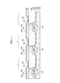
FIG. 1 is a cross-sectional view of an organic light emitting diode display according to an embodiment. -
FIG. 2A is a cross-sectional view showing in detail a structure of a lower electrode and an organic layer in a blue light emitting region. -
FIG. 2B is a cross-sectional view showing in detail a lower electrode and an organic layer in a green light emitting region. -
FIG. 2C is a cross-sectional view showing in detail a lower electrode and a structure of an organic layer in a red light emitting region. -
FIGS. 3 and4 are CIE-based colour coordinates for explaining a colour reproduction rate when the red light emitting region is formed in a non-microcavity structure. - Generally, in order to increase the colour reproduction rate, e.g., the proportion of colours that can be generated with respect to a colour gamut which humans can recognize, of an OLED display, a first electrode having an ITO/Ag/ITO structure is used to transmit a portion of emitted light and resonate another portion of the emitted light.
- In this case, since the red area emits light having a longer wavelength than blue and green areas, the thickness of the organic layer in the red area should be formed to be thicker than that of the organic layer in the blue and green areas in order to generate the desired degree of resonance. Therefore, the thickness of the organic layer formed in each light emitting region becomes non-uniform.
- Hereinafter, an organic light emitting diode display according to an embodiment will be described more fully hereinafter with reference to the accompanying drawings. The disclosed embodiments mainly describe the case where a plurality of pixels defined by blue, green and red light emitting regions are formed on a substrate. Further, the disclosed embodiments describe, by way of example, an active matrix organic light emitting diode display; however, they may be applied to a passive matrix organic light emitting diode display.
- Referring to
FIG. 1 , abuffer layer 210 is formed over asubstrate 200 and an amorphous silicon layer is formed on thebuffer layer 210 by, for example, a deposition method such as PECVD, LPCVD, or the like. In this case, thesubstrate 200 may be an insulating substrate such as glass, quartz, sapphire, etc., and thebuffer layer 210 prevents the amorphous silicon layer from being polluted by impurities diffused from thesubstrate 200. - The amorphous silicon layer may be crystallized by methods such as excimer laser annealing (ELA), sequential lateral solidification (SLS), metal induced crystallization (MIC) or metal induced lateral crystallization (MILC). The amorphous silicon layer may be patterned by a photolithography process to form a
semiconductor layer 220 in a thin layer transistor area in a unit pixel. - Thereafter, a
gate insulating layer 230 is formed over thesubstrate 200 including thesemiconductor layer 220. Thegate insulating layer 230 may be formed at least partially of silicon oxide, silicon nitride or may be formed in a stacked structure thereof. - Next, after a gate electrode material is applied to the upper portion of the
gate insulating layer 230, it is etched to form the patternedgate electrode 240. Thegate electrode 240 is formed to be partially overlapping with thesemiconductor layer 220, and thesemiconductor layer 220 area overlapping with thegate electrode 240 is defined as the channel area. - The
gate electrode 240 may be formed of a single layer of an aluminium alloy of aluminium (Al) or aluminium-neodymium (Al-Nd) or of a multi-layer in which aluminium alloy is stacked on chromium (Cr) or molybdenum (Mo) alloy. - Next, an interlayer insulating layer 250 is formed over the surface. The interlayer insulating layer 250 may use a silicon nitride layer or a silicon oxide layer.
- Next, a metal layer (not shown) is formed on an interlayer insulating layer 250 and is then patterned, thereby forming source/
drain electrodes drain electrodes semiconductor layer 220 through a contact hole formed by partially etching thegate insulating layer 230 and the interlayer insulating layer 250. - The metal layer forms a single layer selected from a group of Mo, W, MoW, AlNd, Ti, Cu, Cu alloy, Al, Al alloy, Ag and Ag alloy, etc. Alternatively, in order to reduce the wire resistance, the metal layer may be formed of one stacking structure selected from one group consisting of a two-layer structure of Mo, Cu, Al or Ag that is a low resistance material or a multilayer structure of two layers or more.
- Then, the silicon nitride layer, the silicon oxide layer or the stacking structure thereof are deposited over the surface at a predetermined thickness to form the
protective layer 270 and then aplanarization layer 280 is formed on theprotective layer 270. Theplanarization layer 280 may be formed at least partially of polyimide, benzocyclobutene based resin, and acrylate. - Thereafter, the
protective layer 270 and theplanarization layer 280 are partially etched to form a via hole that exposes any one of source/drain electrodes lower electrode 290 formed on theplanarization layer 280 is electrically connected to any one of the source/drain electrodes - The
lower electrode 290 is formed in a blue light emitting region (a), a green light emitting region (b), a red light emitting region (c), respectively, and the position in which the light emitting region is formed is not limited thereto. - A
pixel defining layer 295 having an opening is formed on the upper of thelower electrode 290 to expose a portion of thelower electrode 290 through the opening and to form theorganic layer 300 on thelower electrode 290 that is opened. - The
pixel defining layer 295 may be formed at least partially of polyimide, benzocyclobutene series resin, spin-on glass (SOG), and acrylate. - Then, the
upper electrode 310 is formed over thesubstrate 200 to complete the organic light emitting diode. Theupper electrode 310 may be formed at least partially of Li, Ca, LiF/Ca, LiF/Al, Al, Mg and an alloy thereof. - Referring to
FIG. 2A , thelower electrode 290 formed in the blue light emitting region (a) is formed by sequentially stacking the first transparentconductive layer 290a, asemitransparent metal layer 290c, and the second transparentconductive layer 290b and theorganic layer 300 is formed on thelower electrode 290. Thelower electrode 290 of the blue light emitting region (a) may include at least one transparent conductive layer and at least one semitransparent metal layer. This applies to thelower electrode 290 formed in the green light emitting region (b). The first and second transparentconductive layers conductive layer 290a substantially serves as an anode and the second transparentconductive layer 290b serves to match work function, thereby completing thelower electrode 290. - In one embodiment, the first transparent
conductive layer 290a has good light efficiency of blue, green, red within a thickness of about 50 nm to about 150 nm of blue, green, and red and thus, the first transparentconductive layer 290a is formed at the thickness of about 50 nm to about 150 nm. - In one embodiment, the second transparent
conductive layer 290b is formed at about 10 nm or more to sufficiently perform a role of the anode and since it is considered together with the thickness of the organic layer, it may be formed at about 30 nm or less in order to maximize the microcavity (resonance) effect of light generated from the organic light emitting layer. - The
semitransparent metal layer 290c may be formed at least partially of Ag, Al, Ni, Pt and Pd. In one embodiment, the thickness of thesemitransparent metal layer 290c is from about 5 nm to about 20 nm. This range may provide an optimum balance between light transmittance and the functionality as a metal electrode. However, the thickness of thesemitransparent metal layer 290c may be less than about 5 nm or greater than about 20 nm. - The
organic layer 300 may further include at least one of the bluelight emitting layer 303a, thehole injection layer 301 positioned between the bluelight emitting layer 303a and thelower electrode 290 other than the bluelight emitting layer 303a, thehole blocking layer 304 positioned on thehole transport layer 302 and the bluelight emitting layer 303a and theelectron injection layer 305. In this configuration, theorganic layer 300 may be formed at the thickness of about 50 nm to about 60 nm in consideration of the light emitting luminance and the colour reproduction rate. Alternatively, the thickness of theorganic layer 300 may be less than about 50 nm or greater than about 60 nm. - In this case, the thickness of the
hole injection layer 301 and thehole transport layer 302 between thelower electrode 290 and the bluelight emitting layer 303a maximizes the luminance and the microcavity effect, such that they may be formed at a thickness of about 19 nm to about 36 nm in order to maximize the microcavity effect. Again, the thickness of thelayers - Referring to
FIG. 2B , thelower electrode 290 formed in the green light emitting region (b) is formed by sequentially stacking the first transparentconductive layer 290a, thesemitransparent metal layer 290c and the second transparentconductive layer 290b and theorganic layer 300 is formed on thelower electrode 290. The description for thelayers 290a-290c andorganic layer 300 of the blue light emitting region (a) applies to those of the green light emitting region (b), except that inFIG. 2B , theorganic layer 300 includes a greenlight emitting layer 303b instead of the bluelight emitting layer 303a. - Referring to
FIG. 2C , thelower electrode 290 formed in the red light emitting region (c) is formed of the transparent conductive layer and theorganic layer 300 is formed on thelower electrode 290. Thelower electrode 290 may be formed in a single layer or a multilayer structure of the transparent conductive layer. The transparent conductive layer may be formed at least partially of indium tin oxide (ITO), an indium zinc oxide (IZO), tin oxide (TO), and zinc oxide (ZnO) and serves as the anode of thelower electrode 290. - The thickness of the
lower electrode 290 is determined together with the thickness of theorganic layer 300 in order to increase the light emitting luminance and the colour reproduction rate. - The
organic layer 300 includes the redlight emitting layer 303c and may further include at least one of thehole injection layer 301 positioned between thelower electrode 290 and the redlight emitting layer 303c, thehole blocking layer 304 positioned on thehole transport layer 302 and the redlight emitting layer 303c and theelectron injection layer 305. - In this case, the
organic layer 300 may be formed at the thickness of about 50 nm to about 60 nm in consideration of the light emitting luminance, the colour reproduction rate, the thickness of the organic layers of the blue light emitting region and the green light emitting region, etc. However, the red light emitting region can sufficiently satisfy the colour reproduction rate by including only the red light emitting layer and thus, may be formed at the thickness of the red light emitting layer to the thickness of about 60 nm, but is not limited thereto. However, when the red light emitting layer is about 33.6 nm to about 35.6 nm, the light emitting efficiency and the colour reproduction rate is excellent. - According to the above description with reference to
FIGS. 2A to 2C , the lower electrode formed in the blue light emitting region and the green light emitting region has a structure of the first transparent conductive layer/semitransparent metal layer/second transparent conductive layer, but the lower electrode positioned in the red light emitting region is formed of the transparent conductive layer. In other words, a microcavity (resonance) structure is formed in the blue light emitting region and the green light emitting region, but a non-microcavity structure is formed in the red light emitting region. In other words, the red light emitting region does not include a microcavity/resonance structure. - According to a conventional device (not necessarily prior art), in order to form the microcavity structure, the thickness of the organic layer of the red light emitting region is thicker than the thickness of the organic layer of the blue light emitting region and the green light emitting region. In one embodiment, when the red light emitting region forms the non-microcavity structure, the thickness of the organic layers of the blue light emitting region and the green light emitting region is uniform by controlling the thickness of the organic layer of the red light emitting region.
-
FIGS. 3 and4 are CIE-based colour coordinates for explaining a colour reproduction rate when the red light emitting region is formed in a non-microcavity structure, whereinFIG. 3 shows a colour coordinate system according toCIE 1931 colour space, also known as the CIE XYZ colour space andFIG. 4 shows a colour coordinate system according to CIE 1976 (L*, u*, v*) colour space, also known as CIELUV. - The following Table 1 shows results obtained by comparing the colour coordinate, the colour reproduction area, and the colour reproduction rate with the NTSC when the red light emitting region is formed in the non-microcavity structure in the colour coordinate of
FIG. 3 and the following Table 2 shows results obtained by comparing the colour coordinate, the colour reproduction rate, and the colour reproduction rate with the NTSC when the red light emitting region is formed in the non-microcavity structure in the colour coordinate ofFIG. 4 .(Table 1) colour coordinate (x, y) Colour reproduction area Colour reproduction rate blue green red Colour reproduction area Colour reproduction rate Comparative Example (0.140,0.080) (0.210, 0.710) (0.670, 0.330) 0.158 100% embodiment (0.144, 0.077) (0.210, 0.717) (0.668, 0.329) 0.159 100.7% (Table 2) colour coordinate (u', v') Colour reproduction area Colour reproduction rate blue green red Colour reproduction area Colour reproduction rate Comparative Example (0.152, 0.196) (0.076, 0.576) (0.477, 0.528) 0.074 100% embodiment (0.159,0.190) (0.075, 0.577) (0.476, 0.528) 0.075 101.4% - In Tables 1 and 2, the colour reproduction area represents the colour representation range. The higher the number, the wider the colour representation range becomes and the colour reproduction rate relatively represents the colour reproduction rate of the embodiment based on the NTSC reference of 100%.
- Referring to
FIG. 3 and Table 1, when the red light emitting region is formed in the non-microcavity structure, the colour reproduction area is 0.159, which is higher than 0.158 that is a reference of NTSC (National Television System Committee) and the colour reproduction rate is 100.7%, which is relatively higher than the NTSC reference. - In addition, referring to
FIG. 4 and Table 2, when the red light emitting region has the non-microcavity structure, it can be appreciated that the colour representation area is 0.075, which is higher than 0.074 that is the NTSC reference and the colour reproduction rate is 101.4%, which is relatively higher than that of NTSC reference. - Therefore, as in the above embodiment, even though the red light emitting region has the non-microcavity structure, it can be appreciated that the colour reproduction rate satisfies the NTSC reference.
- Meanwhile, although not shown in
FIG. 1 , in order to increase the colour reproduction rate of the red light emitting region, it is possible to form the colour filter or the colour converting layer in the red light emitting region. - The colour filter or the colour converting layer may be implemented by applying the method for forming the generally used colour filter or colour converting layer in the current display device field, may be formed on the
upper electrode 310 in the red light emitting region, and may be formed to correspond to the red light emitting region on an encapsulation substrate (not shown) bonded to thesubstrate 200 ofFIG. 1 . - According to at least one of the disclosed embodiments, the blue and green light emitting regions are formed in a microcavity structure and the red light emitting region is formed in a non-microcavity structure, such that the thickness of the organic layer of the red light emitting region is controlled to make the thickness of the blue light emitting region and the green light emitting region uniform, thereby making it possible to make the thickness of the organic layers of each light emitting region uniform while implementing the full colour.
- It is to be understood that the disclosed embodiments are not considered limiting and cover various modifications and equivalent arrangements included within the scope of the appended claims.
Claims (13)
- An organic light emitting diode (OLED) display comprising:a plurality of pixels comprising a blue light emitting region, a green light emitting region, and a red light emitting region on a substrate and formed by stacking a lower electrode, an organic layer, and an upper electrode, wherein the blue and green light emitting regions are formed to have a microcavity structure and wherein the red light emitting region is formed to have a non-microcavity structure.
- The organic light emitting diode display of claim 1, wherein:the lower electrode of the blue and green light emitting regions is formed of at least one transparent layer and at least one semitransparent layer; andwherein the lower electrode of the red light emitting region is formed of only a transparent layer.
- The organic light emitting diode display of claim 1, wherein the lower electrode of the red light emitting region is formed of one or more transparent conductive layers.
- The organic light emitting diode display of claim 1, 2 or 3, wherein the lower electrode of the blue and green light emitting regions is formed of a first transparent conductive layer, a semitransparent metal layer, and a second transparent conductive layer which are sequentially formed.
- The organic light emitting diode display of claim 4, wherein the thickness of the first transparent conductive layer is from about 50 nm to about 150 nm and the thickness of the second transparent conductive layer is from about 10 nm to about 20 nm.
- The organic light emitting diode display of claim 4, wherein the thickness of the semitransparent metal layer is from about 5 nm to about 20 nm.
- The organic light emitting diode display of any one of the preceding claims, wherein the thickness of the organic layer is from about 50 nm to about 60 nm.
- The organic light emitting diode display of any one of the preceding claims, wherein the organic layers formed on the blue light emitting region, the green light emitting region, and the red light emitting region include a blue emission layer, a green emission layer, and a red emission layer, respectively.
- The organic light emitting diode display of claim 8, wherein the organic layer further includes at least one of a hole injection layer (HIL), a hole transport layer (HTL), a hole blocking layer and an electron injection layer (EIL).
- The organic light emitting diode display of claim 9, wherein the thickness of the hole injection layer (HIL) and the hole transport layer (HTL) is from about 19 nm to about 36 nm.
- The organic light emitting diode display of claim 8, 9 or 10, wherein the thickness of the organic layer in the red light emitting region is substantially the same as the thickness of the red right emitting layer or is about 60 nm.
- The organic light emitting diode display of any one of the preceding claims, further comprising a colour filter or a colour converting layer formed on the upper electrode of the red light emitting region.
- The organic light emitting diode display of any one of claims 1 to 11, further comprising an encapsulation substrate bonded to the substrate and including a colour filter or a colour converting layer formed to correspond to the red light emitting region.
Applications Claiming Priority (1)
| Application Number | Priority Date | Filing Date | Title |
|---|---|---|---|
| KR1020100062880A KR101689336B1 (en) | 2010-06-30 | 2010-06-30 | Organic Light Emitting Diode Display |
Publications (2)
| Publication Number | Publication Date |
|---|---|
| EP2403030A2 true EP2403030A2 (en) | 2012-01-04 |
| EP2403030A3 EP2403030A3 (en) | 2012-04-11 |
Family
ID=44588218
Family Applications (1)
| Application Number | Title | Priority Date | Filing Date |
|---|---|---|---|
| EP11171668A Ceased EP2403030A3 (en) | 2010-06-30 | 2011-06-28 | Organic light emitting diode display |
Country Status (5)
| Country | Link |
|---|---|
| US (1) | US8471276B2 (en) |
| EP (1) | EP2403030A3 (en) |
| JP (1) | JP5755948B2 (en) |
| KR (1) | KR101689336B1 (en) |
| CN (1) | CN102315243B (en) |
Cited By (1)
| Publication number | Priority date | Publication date | Assignee | Title |
|---|---|---|---|---|
| CN114566533A (en) * | 2018-05-09 | 2022-05-31 | 京东方科技集团股份有限公司 | Display panel, manufacturing method thereof and display device |
Families Citing this family (28)
| Publication number | Priority date | Publication date | Assignee | Title |
|---|---|---|---|---|
| US8944018B2 (en) | 2010-07-14 | 2015-02-03 | Ford Global Technologies, Llc | Cooling strategy for engine head with integrated exhaust manifold |
| CN202404339U (en) * | 2012-01-12 | 2012-08-29 | 京东方科技集团股份有限公司 | Array substrate and display device comprising same |
| KR102019063B1 (en) * | 2012-11-12 | 2019-09-06 | 엘지디스플레이 주식회사 | Organic Light Emitting Device |
| KR102046157B1 (en) * | 2012-12-21 | 2019-12-03 | 삼성디스플레이 주식회사 | Organic light emitting diode display and manufacturing method thereof |
| CN103050506A (en) * | 2012-12-28 | 2013-04-17 | 南京中电熊猫液晶显示科技有限公司 | OLED (organic light-emitting diode) display |
| TWI500144B (en) * | 2012-12-31 | 2015-09-11 | Lg Display Co Ltd | Organic light emitting display device and method of manufacturing same |
| US9590017B2 (en) | 2013-01-18 | 2017-03-07 | Universal Display Corporation | High resolution low power consumption OLED display with extended lifetime |
| US10304906B2 (en) | 2013-01-18 | 2019-05-28 | Universal Display Corporation | High resolution low power consumption OLED display with extended lifetime |
| US10243023B2 (en) | 2013-01-18 | 2019-03-26 | Universal Display Corporation | Top emission AMOLED displays using two emissive layers |
| US10580832B2 (en) | 2013-01-18 | 2020-03-03 | Universal Display Corporation | High resolution low power consumption OLED display with extended lifetime |
| US10229956B2 (en) * | 2013-01-18 | 2019-03-12 | Universal Display Corporation | High resolution low power consumption OLED display with extended lifetime |
| KR102131963B1 (en) * | 2013-10-15 | 2020-07-09 | 삼성디스플레이 주식회사 | Organic light-emitting display apparatus |
| US9627649B2 (en) * | 2013-11-26 | 2017-04-18 | Lg Display Co., Ltd. | Organic light emitting display device |
| CN103996694B (en) | 2014-04-25 | 2015-06-10 | 京东方科技集团股份有限公司 | OLED display and preparation method thereof |
| US10700134B2 (en) | 2014-05-27 | 2020-06-30 | Universal Display Corporation | Low power consumption OLED display |
| CN104201187B (en) * | 2014-08-18 | 2017-07-04 | 京东方科技集团股份有限公司 | A kind of OLED display |
| KR102322083B1 (en) | 2015-07-28 | 2021-11-04 | 삼성디스플레이 주식회사 | Organic light emitting diode display and manufacturing method thereof |
| CN105789258B (en) * | 2016-03-24 | 2019-06-11 | 深圳市华星光电技术有限公司 | A kind of OLED display panel and 3D 3 d display device |
| CN106601775B (en) * | 2016-12-19 | 2019-07-02 | 武汉华星光电技术有限公司 | OLED display device and manufacturing method thereof |
| JP6924589B2 (en) * | 2017-03-03 | 2021-08-25 | パイオニア株式会社 | Manufacturing method of light emitting device and light emitting device |
| CN107104129B (en) * | 2017-05-19 | 2021-01-26 | 京东方科技集团股份有限公司 | OLED device manufacturing method, OLED device and display panel |
| CN107134539B (en) * | 2017-07-05 | 2019-07-05 | 固安翌光科技有限公司 | A kind of highly reliable OLED device and preparation method thereof for lighting screen body |
| CN107170905B (en) * | 2017-07-05 | 2019-03-26 | 固安翌光科技有限公司 | A kind of highly reliable passive organic electroluminescent device and preparation method thereof |
| KR102433315B1 (en) * | 2017-12-27 | 2022-08-16 | 삼성전자주식회사 | Ultrasonic transducers embedded organic light emitting diodes panel and display device inculding the same |
| US11114499B2 (en) * | 2018-01-02 | 2021-09-07 | Seoul Viosys Co., Ltd. | Display device having light emitting stacked structure |
| US10797112B2 (en) | 2018-07-25 | 2020-10-06 | Universal Display Corporation | Energy efficient OLED TV |
| KR102668520B1 (en) * | 2018-12-31 | 2024-05-22 | 엘지디스플레이 주식회사 | Transparent display device |
| CN109461386B (en) * | 2019-01-04 | 2024-09-10 | 京东方科技集团股份有限公司 | Display device |
Family Cites Families (15)
| Publication number | Priority date | Publication date | Assignee | Title |
|---|---|---|---|---|
| JP4431958B2 (en) * | 2001-06-01 | 2010-03-17 | セイコーエプソン株式会社 | Color filter and electro-optical device |
| US6911772B2 (en) | 2002-06-12 | 2005-06-28 | Eastman Kodak Company | Oled display having color filters for improving contrast |
| US6861800B2 (en) | 2003-02-18 | 2005-03-01 | Eastman Kodak Company | Tuned microcavity color OLED display |
| JP2005044778A (en) * | 2003-07-19 | 2005-02-17 | Samsung Sdi Co Ltd | Electroluminescent device |
| CN100541857C (en) * | 2003-10-13 | 2009-09-16 | 铼宝科技股份有限公司 | Planar light-emitting element and method for manufacturing the same |
| JP4475942B2 (en) | 2003-12-26 | 2010-06-09 | 三洋電機株式会社 | Display device and manufacturing method thereof |
| US7129634B2 (en) * | 2004-04-07 | 2006-10-31 | Eastman Kodak Company | Color OLED with added color gamut pixels |
| JP2007103349A (en) * | 2005-09-08 | 2007-04-19 | Seiko Epson Corp | Film pattern forming method, organic EL device manufacturing method, color filter substrate manufacturing method, liquid crystal display device manufacturing method |
| JP2007207460A (en) * | 2006-01-31 | 2007-08-16 | Seiko Epson Corp | ORGANIC EL DEVICE, ELECTRONIC DEVICE, AND METHOD FOR MANUFACTURING ORGANIC EL DEVICE |
| JP2007335185A (en) * | 2006-06-14 | 2007-12-27 | Canon Inc | Organic EL element array |
| KR101212224B1 (en) | 2007-01-02 | 2012-12-13 | 삼성디스플레이 주식회사 | Organic Light Emitting Display Device |
| JP2008226718A (en) * | 2007-03-14 | 2008-09-25 | Fuji Electric Holdings Co Ltd | Organic EL device |
| JP5008486B2 (en) * | 2007-07-19 | 2012-08-22 | キヤノン株式会社 | Display device |
| US7825581B2 (en) * | 2008-02-12 | 2010-11-02 | Samsung Electronics Co., Ltd. | Organic light emitting diode display and method for manufacturing the same |
| KR101582937B1 (en) * | 2008-12-02 | 2016-01-08 | 삼성디스플레이 주식회사 | Organic light emitting diode display and method for manufacturing the same |
-
2010
- 2010-06-30 KR KR1020100062880A patent/KR101689336B1/en active Active
-
2011
- 2011-06-20 JP JP2011136608A patent/JP5755948B2/en active Active
- 2011-06-28 EP EP11171668A patent/EP2403030A3/en not_active Ceased
- 2011-06-29 US US13/172,746 patent/US8471276B2/en active Active
- 2011-06-29 CN CN201110187697.4A patent/CN102315243B/en active Active
Non-Patent Citations (1)
| Title |
|---|
| None |
Cited By (1)
| Publication number | Priority date | Publication date | Assignee | Title |
|---|---|---|---|---|
| CN114566533A (en) * | 2018-05-09 | 2022-05-31 | 京东方科技集团股份有限公司 | Display panel, manufacturing method thereof and display device |
Also Published As
| Publication number | Publication date |
|---|---|
| JP2012015107A (en) | 2012-01-19 |
| CN102315243B (en) | 2016-04-27 |
| US8471276B2 (en) | 2013-06-25 |
| EP2403030A3 (en) | 2012-04-11 |
| JP5755948B2 (en) | 2015-07-29 |
| US20120001207A1 (en) | 2012-01-05 |
| CN102315243A (en) | 2012-01-11 |
| KR20120002142A (en) | 2012-01-05 |
| KR101689336B1 (en) | 2016-12-26 |
Similar Documents
| Publication | Publication Date | Title |
|---|---|---|
| EP2403030A2 (en) | Organic light emitting diode display | |
| KR102500276B1 (en) | Organic light emitting display apparatus and the fabrication method thereof | |
| US12402505B2 (en) | Organic light-emitting display apparatus | |
| US10446613B2 (en) | Method of manufacturing an organic light emitting diode display having an auxiliary member in contact with an upper surface of an auxiliary electrode | |
| KR102577525B1 (en) | Display device | |
| US9349987B2 (en) | Method of manufacturing OLED display apparatus | |
| JP6254218B2 (en) | Organic light emitting display | |
| US8872206B2 (en) | Organic light emitting display device and method of manufacturing the same | |
| US9246123B2 (en) | Organic light-emitting display device and method of manufacturing the same | |
| US20170125748A1 (en) | Method of manufacturing organic light emitting display apparatus | |
| KR102316679B1 (en) | ORGANIC LIGHT EMITTING DISPLAY DEVICE and manufacturing method for the same | |
| US20110204369A1 (en) | Organic Light-Emitting Display Device | |
| EP2270866B1 (en) | Organic light emitting diode display device and method of fabricating the same | |
| US9595694B2 (en) | Thin film transistor substrate, organic light-emitting apparatus including the same, method of manufacturing the thin film transistor substrate, and method of manufacturing the organic light-emitting apparatus | |
| CN114725180A (en) | Electroluminescent display device | |
| CN103280539A (en) | Structure of organic light emitting diode, method of manufacturing same and display panel | |
| US20130193456A1 (en) | Organic light emitting diode display | |
| KR20150060200A (en) | Organic Light Emitting Display DEVICE | |
| KR102598743B1 (en) | Organic light emitting display device and method for fabricating the same | |
| KR100943184B1 (en) | Flat panel display device | |
| KR100563065B1 (en) | Electroluminescent display device and manufacturing method thereof | |
| KR100813841B1 (en) | Organic light emitting display device | |
| KR20250046770A (en) | Method of manufaturing thin film and method of manufacturing electroluminiscent display using the same | |
| KR100810630B1 (en) | Organic electroluminescent device and manufacturing method thereof | |
| KR20070111061A (en) | White organic electroluminescent display and manufacturing method |
Legal Events
| Date | Code | Title | Description |
|---|---|---|---|
| AK | Designated contracting states |
Kind code of ref document: A2 Designated state(s): AL AT BE BG CH CY CZ DE DK EE ES FI FR GB GR HR HU IE IS IT LI LT LU LV MC MK MT NL NO PL PT RO RS SE SI SK SM TR |
|
| AX | Request for extension of the european patent |
Extension state: BA ME |
|
| PUAI | Public reference made under article 153(3) epc to a published international application that has entered the european phase |
Free format text: ORIGINAL CODE: 0009012 |
|
| PUAL | Search report despatched |
Free format text: ORIGINAL CODE: 0009013 |
|
| AK | Designated contracting states |
Kind code of ref document: A3 Designated state(s): AL AT BE BG CH CY CZ DE DK EE ES FI FR GB GR HR HU IE IS IT LI LT LU LV MC MK MT NL NO PL PT RO RS SE SI SK SM TR |
|
| AX | Request for extension of the european patent |
Extension state: BA ME |
|
| RIC1 | Information provided on ipc code assigned before grant |
Ipc: H01L 51/52 20060101AFI20120302BHEP |
|
| RAP1 | Party data changed (applicant data changed or rights of an application transferred) |
Owner name: SAMSUNG DISPLAY CO., LTD. |
|
| 17P | Request for examination filed |
Effective date: 20121011 |
|
| 17Q | First examination report despatched |
Effective date: 20130523 |
|
| STAA | Information on the status of an ep patent application or granted ep patent |
Free format text: STATUS: THE APPLICATION HAS BEEN REFUSED |
|
| 18R | Application refused |
Effective date: 20140605 |