EP2401819B1 - Reducing switching noise - Google Patents
Reducing switching noise Download PDFInfo
- Publication number
- EP2401819B1 EP2401819B1 EP10707855.2A EP10707855A EP2401819B1 EP 2401819 B1 EP2401819 B1 EP 2401819B1 EP 10707855 A EP10707855 A EP 10707855A EP 2401819 B1 EP2401819 B1 EP 2401819B1
- Authority
- EP
- European Patent Office
- Prior art keywords
- signal
- gain
- level
- receiver
- noise
- Prior art date
- Legal status (The legal status is an assumption and is not a legal conclusion. Google has not performed a legal analysis and makes no representation as to the accuracy of the status listed.)
- Not-in-force
Links
- 238000004891 communication Methods 0.000 claims description 77
- 238000000034 method Methods 0.000 claims description 28
- 230000001629 suppression Effects 0.000 claims description 26
- 230000001052 transient effect Effects 0.000 claims description 12
- 230000008859 change Effects 0.000 claims description 7
- 238000010586 diagram Methods 0.000 description 8
- 238000001228 spectrum Methods 0.000 description 6
- 230000008901 benefit Effects 0.000 description 4
- 238000004590 computer program Methods 0.000 description 4
- 230000001360 synchronised effect Effects 0.000 description 3
- 238000005516 engineering process Methods 0.000 description 2
- 230000006870 function Effects 0.000 description 2
- 230000008569 process Effects 0.000 description 2
- 239000000969 carrier Substances 0.000 description 1
- 230000006835 compression Effects 0.000 description 1
- 238000007906 compression Methods 0.000 description 1
- 230000001934 delay Effects 0.000 description 1
- 230000003111 delayed effect Effects 0.000 description 1
- 230000007774 longterm Effects 0.000 description 1
- 230000007246 mechanism Effects 0.000 description 1
- 230000004044 response Effects 0.000 description 1
- 238000004088 simulation Methods 0.000 description 1
- 230000001960 triggered effect Effects 0.000 description 1
Images






Classifications
-
- H—ELECTRICITY
- H04—ELECTRIC COMMUNICATION TECHNIQUE
- H04B—TRANSMISSION
- H04B1/00—Details of transmission systems, not covered by a single one of groups H04B3/00 - H04B13/00; Details of transmission systems not characterised by the medium used for transmission
- H04B1/06—Receivers
- H04B1/10—Means associated with receiver for limiting or suppressing noise or interference
- H04B1/109—Means associated with receiver for limiting or suppressing noise or interference by improving strong signal performance of the receiver when strong unwanted signals are present at the receiver input
Definitions
- This invention relates generally to a method and a communication node. More particularly this invention relates to a method and communication node for reducing noise in a communication system utilizing an automatic gain control.
- FIG 4 is a block diagram illustrating an example of an AGC receiver architecture.
- An input signal x(n) is received via the antenna 401, which goes through a receiver antenna filter h 0 (n) 402.
- An attenuator 403 adjusts the input signal and waits for a discontinuity to propagate.
- the adjusted signal proceeds through a band pass filter h 1 (n) 404, and then through a dynamic range limited device 405. Examples of dynamic range limited devices 405 are described above in relation to figures 1 , 2 , and 3 above.
- the signal is processed through an anti alias filter h 2 (n) 406, before it is treated in a wideband power meter 407, where the wideband signal level is measured.
- the measured signal level is controlled by a controller 408 to determine if the signal is acceptable with regards to a threshold and/or range. If the signal is not acceptable, it is transmitted back to the attenuator 403. If the signal is acceptable, it is transmitted to a compensator 409, where the controlled signal together with the signal from the anti alias filter h 2 (n) 406 is processed. The compensator 409 changes the signal gain based on the controlled range. The compensated signal is transmitted through the channel filter h 3 (n), and the output signal y(n) is processed in a demodulator 411 to extract the original information bearing signal from the processed signal y(n).
- Tuning or switching the gain at any processing stage, during the receipt of a continuous signal may add discontinuity to the received signal.
- the discontinuous signal is processed in the subsequent stages, depending on the processing algorithms of these stages, the discontinuity may add noise to the signal and also widen the spectrum of the received signal.
- the problem is increasing when a small wanted signal is received at the same time as a large interferer is received at a frequency which is close to the wanted signal frequency. In this case, the spectrum widening of the large unwanted signal may add a significant amount of noise and interference to the wanted signal. Such a noise pulse and distortion may cause estimation error in the demodulation process and ruin the interpreted symbol.
- the objective is achieved by a method in a first communication node for reducing noise in a communication system utilizing an automatic gain control.
- the first communication node receives a signal from a second communication node. Then, it is determined if a gain level in the received signal is changed. The signal gain is changed. The next step is to determine if an inband interferer is present before transient noise in the signal is suppressed.
- the objective is achieved by a receiver in a first communication node for reducing switching noise in a communication system utilizing an automatic gain control.
- the receiver comprises a receiving unit configured to receive a signal from a second communication node.
- the receiver further comprises a determining unit which is configured to determine if a gain level in the received signal is changed.
- the determining unit is further configured to determine if an inband interferer is present.
- the receiver comprises a changing unit configured to change the signal gain.
- the receiver comprises a suppression unit which is configured to suppress transient noise in the signal.
- the objective is achieved by a communication system for reducing switching noise utilizing an automatic gain control.
- the system comprises a first communication node comprising an antenna configured to receive a signal from a second communication node.
- the system further comprises a receiver which is configured to suppress transient noise.
- the system also comprises a demodulator configured to demodulate the signal.
- system comprises a memory configured to store the demodulated signal.
- the system also comprises a transmitter which is configured to transmit the demodulated signal.
- the signal quality of the communication system is improved.
- the device reduces the probability for the demodulator of detecting erroneous symbols due to AGC switching noise and attenuator - compensator mismatch.
- Another advantage of the present solution is that the signal treated in the demodulation process has no estimation errors which give a correct interpretation of the signal.
- the present solution is related to a receiver with automatic gain control which continuously adjusts the receiver gain, moving the input signal into the dynamic range.
- the device waits for the discontinuity to propagate, first to a compensator unit and a channel filter, then to a suppression unit, where it suppresses the switching noise by exchanging the noise pulse in the signal with zeroes. The suppression only is applied if the wanted signal exceeds a threshold level.
- FIG. 5 is a schematic block diagram illustrating embodiments of a communication network 500.
- the network may use technologies such as e.g. LTE, UMTS or GSM etc.
- the network 500 comprises at least one first communication node 501 and at least one second communication node 503.
- the first communication node 501 may be e.g. a base station, eNodeB, etc.
- the second communication node 503 may be any suitable communication device or computational device with communication capabilities, for instance but not limited to user equipment, mobile phone, smart phone, personal digital assistant (PDA), laptop, MP3 player, portable DVD player or similar media content devices, digital camera, or even stationary devices such as a PC.
- PDA personal digital assistant
- the first communication node 501 and the second communication node 503 communicates with each other using any suitable kind of wired (not shown) or wireless communication link 505.
- the communication link 505 may use any suitable protocol depending on type and level of layer, e.g. as indicated by the OSI model, as understood by the person skilled in the art.
- the first communication node 501 may be connected to a core network 507 providing e.g. internet services to the second communication node 503.
- the network 500 is configured with cabling, routers, switches, and other network building elements (not shown) as understood by the skilled person, for instance as used for building an Ethernet or WAN network.
- FIG. 6 is a block diagram illustrating the present solution for extending the AGC receiver with a synchronized noise suppression device.
- the units 601 - 610 corresponds to the units 401 - 410 in figure 4 , and will therefore not be described again in detail with reference to figure 6 .
- the Automatic Gain Control (AGC) receiver illustrated in figure 6 operates by redistributing gain around the dynamic range limited device 605 to keep the signal within an operating range.
- the controller unit 608 monitors the wideband power level, P Wideband measured by the wideband power meter 607, and automatically adjusts the receiver gain through the attenuator 603. During these adjustments, a discontinuity may be generated in the signal.
- the discontinuity may be distorted in frequency, phase and amplitude by a mismatch between attenuation and compensation.
- the present solution extends the AGC by adding a device to synchronize, through delays, a signal suppression that zeros the signal for part of, or the whole of, the noise burst. This is illustrated in Figure 9 where noise is suppressed during a part of the noise burst
- the device also measures the power level within the channel bandwidth, P Inband , 612 to determine if the attenuator 603 is triggered by the wanted signal or by the interferer.
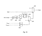
- Figure 10 show an example how the synchronized noise suppressor and control may be realized.
- the delay elements z -d0 1001 and z -d1 1002 and XOR logic 1003 control the start, d0, and duration, d1, of the suppression by toggling a register 1004.
- the comparator 1005 chooses, by comparing the inband signal, P i nband , and the threshold, P threshold , if suppression shall be used with MUX 1006. Suppression is applied using MUX 1007.
- the first communication node 501 receives a signal from the second communication node 503 over the communication link 505.
- the receiver may be a wideband receiver.
- the signal may be received continuously or when requested by the first communication node 501.
- a wideband signal level of the received signal is measured.
- the wideband signal level is measured by using the wideband power meter 607.
- a range of the measured wideband signal level is evaluated by the controller 608. If the wideband signal level is within the range (true), it returns to step 1102. If the wideband signal level is outside the range (false), the method proceeds to step 1104.
- a signal gain in an analogue domain is changed based on the evaluated range.
- the suppression control signal is delayed for a time equal to the propagation delay of the filter h 3 (n) 610.
- the signal gain is restored in a digital domain.
- An inband signal level in the restored signal gain is measured.
- the level is measured by the inband power meter 612 placed after the channel filter h 3 (n) 610.
- the inband signal level is measured with respect to a threshold level, P Threshold .
- the threshold level is set to match the intersection point between the two bit error rate plots shown in Figure 12.
- Figure 12 gives example of threshold level for inband (channel bandwidth) power. These bit error rate plots may be based upon simulations or statistical data. If the level exceeds the threshold (true), the method proceeds to step 1108 where the transient noise in the restored signal is suppressed. If the inband signal level does not exceed the threshold (false), the method proceeds to the start, step 1101.
- the threshold, P Threshold may be a constant value or a range, and may be based on for instance bit error rate.
- the transient noise in the restored signal is suppressed, i.e. the noise is zeroed.
- the synchronization is done by delaying the suppressed signal for a time corresponding to the duration of the suppressed signal.
- the suppression is turned off. After the suppression is turned off, the method may go back to the start to receive a new signal.
- the suppression is disabled when the threshold is exceeded, giving the best performance regarding e.g. bit error rate.
- the suppression device shall, when enabled, output a signal corresponding to zero value according in the signal representation. When disabled it shall output the input signal unmodified.
- FIG. 13 is a flowchart describing the present method in the first communication node 501 for reducing noise in a communication system 500 utilizing automatic gain control.
- the first communication node 501 may be a base station and the second communication node 503 may be a user equipment.
- the method comprises the steps to be performed by the application in the first communication node 501 and which steps may be performed in any suitable order:
- the first communication node 501 receives a signal from a second communication node 503.
- the first communication node 501 determined if a signal gain level is changed.
- the first communication node 501 may measure a wideband signal level of the received signal.
- the first communication node 501 may evaluate the measured wideband signal level.
- the signal gain is changed.
- the first communication node 501 may change the signal gain in an analogue domain.
- the first communication node may restore the signal gain to a digital domain.
- the first communication node 501 determines if an inband interferer is present.
- the first communication node 501 may measure an inband signal level in the restored signal gain.
- the first communication node 501 suppresses transient noise in the signal.
- the first communication node 501 may compare the inband signal level with a threshold level.
- the comparing may be based on bit error rate.
- the first communication node 501 may delay the signal in time.
- the time may be in correspondence with the duration of the suppressed noise.
- the first communication node 501 may disable the suppression.
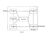
- the system 500 comprises receiver 1400 in a first communication node as shown in Figure 14 .
- the receiver 1400 comprises a receiving unit 1401 configured to receive a signal 1407 from a second communication node 503.
- the receiver 1400 also comprises a determining unit 1402 configured to determine if a gain level is changed.
- the determining unit 1402 is further configured to determine if an inband interferer is present. Further, the determining unit 1402 may be configured to measure a wideband signal level of the received signal, and to evaluate the measured wideband signal level. The determining unit 1402 may be further configured to measure an inband signal level in the restored signal gain.
- the receiver 1400 further comprises a changing unit 1403 which is configured to change the signal gain.
- the changing unit 1403 may be further configured to change the signal gain in an analogue domain.
- the receiver 1400 may comprise a restoring unit 1405 which may be configured to restore the signal gain to a digital domain.
- the receiver 1400 comprises a suppression unit 1404 configured to suppress transient noise in the signal.
- the suppression unit 1404 may be further configured to compare the inband signal level with a threshold level.
- the suppression unit 1404 may even further be configured to delay the signal in time. The time may be in correspondence with the duration of the suppressed noise.
- the suppression unit 1404 may also be configured to disable the suppression.
- the system 500 comprises a first communication node 501.
- the first communication node 501 comprising an antenna configured to receive a signal from a second communication node 503 and the receiver 1400 which configured to suppress transient noise.
- the first communication node 501 further comprises a demodulator configured to demodulate the signal, a memory configured to store the demodulated signal, and a transmitter configured to transmit the demodulated signal.
- the wireless communication system may be for instance based on Long Term Evolution (LTE) or Universal Mobile Telecommunications System (UMTS).
- the present mechanism for reducing switching noise in a wireless communication system 500 may be implemented through one or more processors, such as a processor 1406 in the receiver 1400 depicted in Figure 14 , together with computer program code for performing the functions of the present solution.
- the processor may be for example a Digital Signal Processor (DSP), Application Specific Integrated Circuit (ASIC) processor, Field-programmable gate array (FPGA) processor or micro processor.
- DSP Digital Signal Processor
- ASIC Application Specific Integrated Circuit
- FPGA Field-programmable gate array
- the program code mentioned above may also be provided as a computer program product, for instance in the form of a data carrier carrying computer program code for performing the present solution when being loaded into the first communication node 1400.
- One such carrier may be in the form of a CD ROM disc. It is however feasible with other data carriers such as a memory stick.
- the computer program code may furthermore be provided as pure program code on a server and downloaded to the receiver 1400 comprised in the first communication node 501.
Landscapes
- Engineering & Computer Science (AREA)
- Computer Networks & Wireless Communication (AREA)
- Signal Processing (AREA)
- Noise Elimination (AREA)
- Circuits Of Receivers In General (AREA)
Description
- This invention relates generally to a method and a communication node. More particularly this invention relates to a method and communication node for reducing noise in a communication system utilizing an automatic gain control.
- For receivers in radio communication systems, it is important to control the dynamic range of the signals at each processing stage in the receiver. High performance receiver designs utilize Automatic Gain Control (AGC) to tune the gain distribution, so the total received signal does not saturate at any stage in the receiver chain. Examples of devices that impact on the dynamic range are nonlinear amplifiers, limiting amplifiers, and Analogue-to-Digital (A/D)-Digital-to-Analogue (D/A) converters etc.
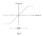
Figure 1 illustrates an example of a nonlinear amplifier. The characteristics seen in the figure are caused by noise floor and gain compression.Figure 2 illustrates an example of a limiting amplifier where the characteristics seen are caused by limited output.Figure 3 illustrates the dynamic range limited device characteristic of an A/D-D/A Converter. -
Figure 4 is a block diagram illustrating an example of an AGC receiver architecture. An input signal x(n) is received via theantenna 401, which goes through a receiver antenna filter h0(n) 402. Anattenuator 403 adjusts the input signal and waits for a discontinuity to propagate. The adjusted signal proceeds through a band pass filter h1(n) 404, and then through a dynamic rangelimited device 405. Examples of dynamic rangelimited devices 405 are described above in relation tofigures 1 ,2 , and3 above. The signal is processed through an anti alias filter h2(n) 406, before it is treated in awideband power meter 407, where the wideband signal level is measured. The measured signal level is controlled by acontroller 408 to determine if the signal is acceptable with regards to a threshold and/or range. If the signal is not acceptable, it is transmitted back to theattenuator 403. If the signal is acceptable, it is transmitted to acompensator 409, where the controlled signal together with the signal from the anti alias filter h2(n) 406 is processed. Thecompensator 409 changes the signal gain based on the controlled range. The compensated signal is transmitted through the channel filter h3(n), and the output signal y(n) is processed in ademodulator 411 to extract the original information bearing signal from the processed signal y(n). - Tuning or switching the gain at any processing stage, during the receipt of a continuous signal, may add discontinuity to the received signal. When the discontinuous signal is processed in the subsequent stages, depending on the processing algorithms of these stages, the discontinuity may add noise to the signal and also widen the spectrum of the received signal. The problem is increasing when a small wanted signal is received at the same time as a large interferer is received at a frequency which is close to the wanted signal frequency. In this case, the spectrum widening of the large unwanted signal may add a significant amount of noise and interference to the wanted signal. Such a noise pulse and distortion may cause estimation error in the demodulation process and ruin the interpreted symbol.
- Document
US 2008/0279393 discloses a method in a communication node for suppressing noise in a communication system using automatic gain control. - It is thus an object of the present invention to provide improved signal quality in a communication system. The present invention is defined by the features of
independent claims 1 and 8. - According to a first aspect of the present solution, the objective is achieved by a method in a first communication node for reducing noise in a communication system utilizing an automatic gain control. At first, the first communication node receives a signal from a second communication node. Then, it is determined if a gain level in the received signal is changed. The signal gain is changed. The next step is to determine if an inband interferer is present before transient noise in the signal is suppressed.
- According to a second aspect of the present solution, the objective is achieved by a receiver in a first communication node for reducing switching noise in a communication system utilizing an automatic gain control. The receiver comprises a receiving unit configured to receive a signal from a second communication node.
- The receiver further comprises a determining unit which is configured to determine if a gain level in the received signal is changed. The determining unit is further configured to determine if an inband interferer is present.
- The receiver comprises a changing unit configured to change the signal gain.
- Further, the receiver comprises a suppression unit which is configured to suppress transient noise in the signal.
- According to a third aspect of the present solution, the objective is achieved by a communication system for reducing switching noise utilizing an automatic gain control. The system comprises a first communication node comprising an antenna configured to receive a signal from a second communication node.
- The system further comprises a receiver which is configured to suppress transient noise.
- The system also comprises a demodulator configured to demodulate the signal.
- Further, the system comprises a memory configured to store the demodulated signal.
- The system also comprises a transmitter which is configured to transmit the demodulated signal.
- Thanks to suppression of the switching noise by exchanging the noise pulse in the signal with zeroes, the signal quality of the communication system is improved.
- The present technology affords many advantages, for which a non-exhaustive list of examples follows:
- The device reduces the probability for the demodulator of detecting erroneous symbols due to AGC switching noise and attenuator - compensator mismatch.
- Another advantage of the present solution is that the signal treated in the demodulation process has no estimation errors which give a correct interpretation of the signal.
- The present invention is not limited to the features and advantages mentioned above. A person skilled in the art will recognize additional features and advantages upon reading the following detailed description.
- The invention will now be further described in more detail in the following detailed description by reference to the appended drawings illustrating embodiments of the invention and in which:
- Fig. 1
- is a graph illustrating characteristics of an example of a dynamic range limited device.
- Fig. 2
- is a graph illustrating characteristics of an example of a dynamic range limited device.
- Fig. 3
- is a graph illustrating characteristics of an example of a dynamic range limited device.
- Fig. 4
- is a block diagram illustrating an example of an AGC receiver architecture.
- Fig. 5
- is a schematic block diagram illustrating embodiments of a communication network.
- Fig. 6
- is a schematic block diagram illustrating embodiments of an AGC receiver architecture.
- Fig. 7
- is a graph illustrating examples of signal spectra.
- Fig. 8
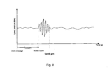
- is a graph illustrating noise burst after AGC switching.
- Fig. 9
- is a graph illustrating suppression of noise.
- Fig. 10
- is a block diagram illustrating embodiments of a synchronized noise suppressor.
- Fig. 11
- is a flowchart depicting embodiments of a method in a communications network.
- Fig. 12
- is a graph illustrating examples of threshold level for inband power.
- Fig. 13
- is a flowchart depicting embodiments of a method in a communications network.
- Fig. 14
- is a schematic block diagram illustrating embodiments of a receiver.
- The drawings are not necessarily to scale, emphasize is instead being placed upon illustrating the principle of the invention.
- The present solution is related to a receiver with automatic gain control which continuously adjusts the receiver gain, moving the input signal into the dynamic range. When an adjustment in an attenuator unit occurs, the device waits for the discontinuity to propagate, first to a compensator unit and a channel filter, then to a suppression unit, where it suppresses the switching noise by exchanging the noise pulse in the signal with zeroes. The suppression only is applied if the wanted signal exceeds a threshold level.
-
Figure 5 is a schematic block diagram illustrating embodiments of acommunication network 500. The network may use technologies such as e.g. LTE, UMTS or GSM etc. Thenetwork 500 comprises at least onefirst communication node 501 and at least onesecond communication node 503. Thefirst communication node 501 may be e.g. a base station, eNodeB, etc. Thesecond communication node 503 may be any suitable communication device or computational device with communication capabilities, for instance but not limited to user equipment, mobile phone, smart phone, personal digital assistant (PDA), laptop, MP3 player, portable DVD player or similar media content devices, digital camera, or even stationary devices such as a PC. Thefirst communication node 501 and thesecond communication node 503 communicates with each other using any suitable kind of wired (not shown) orwireless communication link 505. Thecommunication link 505 may use any suitable protocol depending on type and level of layer, e.g. as indicated by the OSI model, as understood by the person skilled in the art. - The
first communication node 501 may be connected to acore network 507 providing e.g. internet services to thesecond communication node 503. - It should be appreciated that the
network 500 is configured with cabling, routers, switches, and other network building elements (not shown) as understood by the skilled person, for instance as used for building an Ethernet or WAN network. -
Figure 6 is a block diagram illustrating the present solution for extending the AGC receiver with a synchronized noise suppression device. The units 601 - 610 corresponds to the units 401 - 410 infigure 4 , and will therefore not be described again in detail with reference tofigure 6 . The Automatic Gain Control (AGC) receiver illustrated infigure 6 operates by redistributing gain around the dynamic rangelimited device 605 to keep the signal within an operating range. Thecontroller unit 608 monitors the wideband power level, PWideband measured by thewideband power meter 607, and automatically adjusts the receiver gain through theattenuator 603. During these adjustments, a discontinuity may be generated in the signal. The discontinuity may be distorted in frequency, phase and amplitude by a mismatch between attenuation and compensation. If there is an interferer present it may get widened in spectrum by the discontinuity, generating a noise pulse into the wanted signal. This is illustrated inFigure 7 which shows examples of the signal spectra. When a discontinuity occurs, the interferer signal may be widened and leak into the wanted signal spectrum. - This burst caused by the discontinuity and noise may get widened in time due to the impulse response of the signal processing filters represented by the filters h1(n), h2(n) and h3(n) in
Figure 4 and6 . Even though the compensator adjusts according to theattenuator 603, the distortion has already been added to the wanted signal. This is illustrated inFigure 8 showing noise burst after AGC switching. - The present solution extends the AGC by adding a device to synchronize, through delays, a signal suppression that zeros the signal for part of, or the whole of, the noise burst. This is illustrated in
Figure 9 where noise is suppressed during a part of the noise burst - The device also measures the power level within the channel bandwidth, PInband, 612 to determine if the
attenuator 603 is triggered by the wanted signal or by the interferer.Figure 10 show an example how the synchronized noise suppressor and control may be realized. Thedelay elements z -d0 1001 andz -d1 1002 andXOR logic 1003 control the start, d0, and duration, d1, of the suppression by toggling aregister 1004. Thecomparator 1005 chooses, by comparing the inband signal, Pinband , and the threshold, Pthreshold , if suppression shall be used withMUX 1006. Suppression is applied usingMUX 1007. - The present solution method for reducing noise in a wireless communication system according to some embodiments will now be described with reference to flowchart depicted in
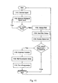
Figure 11 , with reference toFigure 5 illustrating embodiments of a communication network,Figure 6 illustrating embodiments of an AGC receiver architecture andFigure 12 illustrating example of threshold levels. The method comprises the following steps, which steps may as well be carried out in another suitable order than described below: - The
first communication node 501 receives a signal from thesecond communication node 503 over thecommunication link 505. The receiver may be a wideband receiver. The signal may be received continuously or when requested by thefirst communication node 501. - A wideband signal level of the received signal is measured. The wideband signal level is measured by using the
wideband power meter 607. - A range of the measured wideband signal level is evaluated by the
controller 608. If the wideband signal level is within the range (true), it returns to step 1102. If the wideband signal level is outside the range (false), the method proceeds to step 1104. - A signal gain in an analogue domain is changed based on the evaluated range.
- When a change in AGC is initiated in steps 1101 -1105, the suppression control signal is delayed for a time equal to the propagation delay of the filter h3(n) 610.
- The signal gain is restored in a digital domain.
- An inband signal level in the restored signal gain is measured. The level is measured by the
inband power meter 612 placed after the channel filter h3(n) 610. - The inband signal level is measured with respect to a threshold level, PThreshold. The threshold level is set to match the intersection point between the two bit error rate plots shown in
Figure 12. Figure 12 gives example of threshold level for inband (channel bandwidth) power. These bit error rate plots may be based upon simulations or statistical data. If the level exceeds the threshold (true), the method proceeds to step 1108 where the transient noise in the restored signal is suppressed. If the inband signal level does not exceed the threshold (false), the method proceeds to the start,step 1101. The threshold, PThreshold, may be a constant value or a range, and may be based on for instance bit error rate. - The transient noise in the restored signal is suppressed, i.e. the noise is zeroed.
- The synchronization is done by delaying the suppressed signal for a time corresponding to the duration of the suppressed signal.
- The suppression is turned off. After the suppression is turned off, the method may go back to the start to receive a new signal.
- The suppression is disabled when the threshold is exceeded, giving the best performance regarding e.g. bit error rate.
- The suppression device shall, when enabled, output a signal corresponding to zero value according in the signal representation. When disabled it shall output the input signal unmodified.
- The method described above will now be described seen from the perspective of the
first communication node 501.Figure 13 is a flowchart describing the present method in thefirst communication node 501 for reducing noise in acommunication system 500 utilizing automatic gain control. Thefirst communication node 501 may be a base station and thesecond communication node 503 may be a user equipment. The method comprises the steps to be performed by the application in thefirst communication node 501 and which steps may be performed in any suitable order: - The
first communication node 501 receives a signal from asecond communication node 503. - The
first communication node 501 determined if a signal gain level is changed. - This is an optional step to be performed as a substep of
step 1302. Thefirst communication node 501 may measure a wideband signal level of the received signal. - This is an optional step to be performed as a substep of
step 1302. Thefirst communication node 501 may evaluate the measured wideband signal level. - The signal gain is changed.
- This is an optional step to be performed as a substep of
step 1303. Thefirst communication node 501 may change the signal gain in an analogue domain. - This is an optional step. The first communication node may restore the signal gain to a digital domain.
- The
first communication node 501 determines if an inband interferer is present. - This is an optional step to be performed as a substep of
step 1305. Thefirst communication node 501 may measure an inband signal level in the restored signal gain. - The
first communication node 501 suppresses transient noise in the signal. - This is an optional step to be performed as a substep of
step 1306. Thefirst communication node 501 may compare the inband signal level with a threshold level. - The comparing may be based on bit error rate.
- This is an optional step to be performed as a substep of
step 1306. Thefirst communication node 501 may delay the signal in time. The time may be in correspondence with the duration of the suppressed noise. - This is an optional step to be performed as a substep of
step 1306. Thefirst communication node 501 may disable the suppression. - To perform the method steps shown in
figure 13 for reducing noise in acommunication system 500 utilizing an automatic gain control. Thesystem 500 comprisesreceiver 1400 in a first communication node as shown inFigure 14 . - The
receiver 1400 comprises areceiving unit 1401 configured to receive asignal 1407 from asecond communication node 503. - The
receiver 1400 also comprises a determiningunit 1402 configured to determine if a gain level is changed. The determiningunit 1402 is further configured to determine if an inband interferer is present. Further, the determiningunit 1402 may be configured to measure a wideband signal level of the received signal, and to evaluate the measured wideband signal level. The determiningunit 1402 may be further configured to measure an inband signal level in the restored signal gain. - The
receiver 1400 further comprises a changingunit 1403 which is configured to change the signal gain. The changingunit 1403 may be further configured to change the signal gain in an analogue domain. - The
receiver 1400 may comprise a restoringunit 1405 which may be configured to restore the signal gain to a digital domain. - The
receiver 1400 comprises asuppression unit 1404 configured to suppress transient noise in the signal. Thesuppression unit 1404 may be further configured to compare the inband signal level with a threshold level. Thesuppression unit 1404 may even further be configured to delay the signal in time. The time may be in correspondence with the duration of the suppressed noise. Thesuppression unit 1404 may also be configured to disable the suppression. - The method and
receiver 1400 described above will now be described in the perspective of acommunication system 500 for reducing noise utilizing an automatic gain control. Thesystem 500 comprises afirst communication node 501. Thefirst communication node 501 comprising an antenna configured to receive a signal from asecond communication node 503 and thereceiver 1400 which configured to suppress transient noise. Thefirst communication node 501 further comprises a demodulator configured to demodulate the signal, a memory configured to store the demodulated signal, and a transmitter configured to transmit the demodulated signal. The wireless communication system may be for instance based on Long Term Evolution (LTE) or Universal Mobile Telecommunications System (UMTS). - The present mechanism for reducing switching noise in a
wireless communication system 500 may be implemented through one or more processors, such as aprocessor 1406 in thereceiver 1400 depicted inFigure 14 , together with computer program code for performing the functions of the present solution. The processor may be for example a Digital Signal Processor (DSP), Application Specific Integrated Circuit (ASIC) processor, Field-programmable gate array (FPGA) processor or micro processor. The program code mentioned above may also be provided as a computer program product, for instance in the form of a data carrier carrying computer program code for performing the present solution when being loaded into thefirst communication node 1400. One such carrier may be in the form of a CD ROM disc. It is however feasible with other data carriers such as a memory stick. The computer program code may furthermore be provided as pure program code on a server and downloaded to thereceiver 1400 comprised in thefirst communication node 501. - It should be noted that the word "comprising" does not exclude the presence of other elements or steps than those listed and the words "a" or "an" preceding an element do not exclude the presence of a plurality of such elements. The invention can at least in part be implemented in either software or hardware. It should further be noted that any reference signs do not limit the scope of the claims, and that several "means", "devices", and "units" may be represented by the same item of hardware.
- The above mentioned and described embodiments are only given as examples and should not be limiting to the present invention. Other solutions, uses, objectives, and functions within the scope of the invention as claimed in the below described patent claims should be apparent for the person skilled in the art.
Claims (11)
- A method in a first communication node (501) for suppressing noise in a communication system (500) utilizing an automatic gain control,
the method comprises the steps of:receiving (1101, 1301) a signal from a second communication node (503); anddetermining (1102, 1302) if a gain level of the received signal is changed; andwherein the step of determining (1302) if a gain level is changed further comprises:measuring (1102, 1302a) a wideband signal level of the received signal; andevaluating (1103, 1302b) if the measured wideband signal level is outside a range;and wherein the method further comprises the steps of:changing (1104, 1303) the signal gain if the evaluated signal level is outside the range;determining (1107, 1305) if an inband interferer is present; suppressing (1108, 1306), using a suppression unit, transient noise in the signal if the inband interferer is present; anddisabling (1110, 1306c) the suppressing. - The method according to claim 1, wherein the step of changing (1303) the signal gain further comprising:changing (1104, 1303a) the signal gain in an analogue domain;and wherein the method further comprises the step of:restoring (1106,1304) the signal gain to a digital domain.
- The method according to claim 2, wherein the step of determining (1305) a present of an inband interferer further comprises
measuring (1107, 1305a) an inband signal level in the restored signal gain. - The method according to claim 3, wherein the step of suppressing (1306) transient noise comprises:comparing (1107, 1306a) the inband signal level with a threshold level.
- The method according to claim 4,
wherein the comparing is based on bit error rate. - The method according to any of the claims 1 - 5, wherein the step of suppressing (1306) transient noise comprises:delaying (1306b) the signal in time, wherein the time is in correspondence with a duration of the suppressed noise.
- A receiver (1400) in a first communication node (501) for suppressing noise in a communication system utilizing an automatic gain control,
the receiver comprises- a receiving unit (1401) configured to receive a signal (1407) from a second communication node (503);- a determining unit (1402) configured todetermine if a gain level in the received signal is changed;measure a wideband signal level of the received signal; and to evaluate if the measured wideband signal is outside a range;- a changing unit (1403) configured to change the signal gain if the evaluated signal level is outside the range;the determining unit (1402) is further configured to determine if an inband interferer is present; and- a suppression unit (1404) configured to suppress transient noise in the signal if the inband interferer is present and to disable the suppression. - The receiver (1400) according to claim 7, wherein the changing unit (1403) is further configured to change the signal gain in an analogue domain;
and wherein the receiver (1400) further comprises
a restoring unit (1405) configured to restore the signal gain to a digital domain. - The receiver (1400) according to claim 8, wherein the determining unit (1402) is further configured to measure an inband signal level in the restored signal gain.
- The receiver (1400) according to claim 9, wherein the suppression unit (1404) is further configured to
compare the inband signal level with a threshold level. - The receiver (1400) according to any of the claims 7 - 10, wherein the suppression unit (1404) is further configured to
delay the signal in time, wherein the time is in correspondence with the duration of the suppressed noise.
Applications Claiming Priority (2)
| Application Number | Priority Date | Filing Date | Title |
|---|---|---|---|
| US15567109P | 2009-02-26 | 2009-02-26 | |
| PCT/EP2010/052191 WO2010097359A1 (en) | 2009-02-26 | 2010-02-22 | Reducing switching noise |
Publications (2)
| Publication Number | Publication Date |
|---|---|
| EP2401819A1 EP2401819A1 (en) | 2012-01-04 |
| EP2401819B1 true EP2401819B1 (en) | 2014-04-09 |
Family
ID=42126517
Family Applications (1)
| Application Number | Title | Priority Date | Filing Date |
|---|---|---|---|
| EP10707855.2A Not-in-force EP2401819B1 (en) | 2009-02-26 | 2010-02-22 | Reducing switching noise |
Country Status (3)
| Country | Link |
|---|---|
| US (1) | US8582700B2 (en) |
| EP (1) | EP2401819B1 (en) |
| WO (1) | WO2010097359A1 (en) |
Families Citing this family (1)
| Publication number | Priority date | Publication date | Assignee | Title |
|---|---|---|---|---|
| US8744022B2 (en) | 2009-12-18 | 2014-06-03 | Telefonaktiebolaget Lm Ericsson (Publ) | Glitch mitigation in a radio receiver |
Family Cites Families (11)
| Publication number | Priority date | Publication date | Assignee | Title |
|---|---|---|---|---|
| US7120410B2 (en) | 2001-09-28 | 2006-10-10 | Broadcom Corporation | LNA gain adjustment in an RF receiver to compensate for intermodulation interference |
| GB2381415B (en) * | 2001-10-24 | 2003-12-10 | Motorola Inc | Receiver circuit for use in radio communications and communications unit including such a circuit |
| US7299021B2 (en) * | 2001-12-28 | 2007-11-20 | Nokia Corporation | Method and apparatus for scaling the dynamic range of a receiver for continuously optimizing performance versus power consumption |
| JP2005286787A (en) * | 2004-03-30 | 2005-10-13 | Sanyo Electric Co Ltd | Noise eliminating circuit |
| EP1605587A1 (en) * | 2004-06-07 | 2005-12-14 | Infineon Technologies AG | A receiver comprised in a radio communication system |
| EP1638211A1 (en) * | 2004-09-16 | 2006-03-22 | Dibcom | Impulse noise correction |
| CN101129022B (en) * | 2005-02-25 | 2011-04-13 | 株式会社Ntt都科摩 | Receivers and Transmitters for Networks with Decentralized Media Access Control |
| US7440737B2 (en) | 2005-08-30 | 2008-10-21 | Freescale Semiconductor, Inc. | Noise blanker control |
| US8542638B2 (en) * | 2006-04-20 | 2013-09-24 | Microchip Technology Incorporated | System and method for interference identification and frequency allocation |
| US8295371B2 (en) * | 2006-07-14 | 2012-10-23 | Qualcomm Incorporated | Multi-carrier receiver for wireless communication |
| US20090016471A1 (en) * | 2007-07-10 | 2009-01-15 | Ravikiran Rajagopal | Impulse Noise Detection and Mitigation In Receivers |
-
2010
- 2010-02-22 EP EP10707855.2A patent/EP2401819B1/en not_active Not-in-force
- 2010-02-22 WO PCT/EP2010/052191 patent/WO2010097359A1/en not_active Ceased
- 2010-02-22 US US13/202,847 patent/US8582700B2/en not_active Expired - Fee Related
Also Published As
| Publication number | Publication date |
|---|---|
| EP2401819A1 (en) | 2012-01-04 |
| US20110305305A1 (en) | 2011-12-15 |
| US8582700B2 (en) | 2013-11-12 |
| WO2010097359A1 (en) | 2010-09-02 |
Similar Documents
| Publication | Publication Date | Title |
|---|---|---|
| JP5613829B2 (en) | Base station calibration | |
| TWI527410B (en) | Automatic gain control circuit and receiver and wireless device comprising the same | |
| CN106416089B (en) | A device, equipment and method related to a transceiver | |
| CA2232754A1 (en) | Gain control method and receiver | |
| WO2007126369A2 (en) | Adjacent channel interference suppression using beamforming | |
| US9544862B2 (en) | Method and device for performing automatic gain control | |
| EP2426878B1 (en) | Bias removal of radio link quality estimates | |
| JPH04160844A (en) | Demodulator | |
| US6768441B2 (en) | Methods of receiving communications signals including a plurality of digital filters having different bandwidths and related receivers | |
| WO2002056511A1 (en) | Suppression of periodic interference in a communications system | |
| KR19990063772A (en) | Method and apparatus for reducing distortion effect in determining signal availability | |
| US8582700B2 (en) | Reducing switching noise | |
| CN101682341B (en) | Increasing sensitivity of radio receiver | |
| JP7593418B2 (en) | Communication channel estimation method, wireless communication system, transmitting device, and receiving device | |
| EP4441929A1 (en) | Reduction of interference caused by downlink aggressors | |
| CN101645724A (en) | Method, device and mobile terminal for optimizing decoding performance | |
| KR101482737B1 (en) | Method of detecting Sync-signal in TDD system and Apparatus there-of | |
| JP5206290B2 (en) | Mobile communication receiver | |
| JP2011082904A (en) | Serial receiving circuit, serial receiving device, radio base station, mobile communication device, and interference compensation method | |
| US10917130B1 (en) | Signal receiving apparatus and method having anti-RFI mechanism | |
| US20140355654A1 (en) | Radio Receiver for Detecting an Additive White Gaussian Noise Channel | |
| KR100360775B1 (en) | Base station in cdma communication system for wide band comprising phase equalizer bank and method of compensating phase therein | |
| KR101015716B1 (en) | Receiving device and signal receiving method of mobile terminal in mobile communication system | |
| KR20240125445A (en) | Autonomous determination of discontinuous transmit opportunities by ethernet based radios | |
| WO2012068500A1 (en) | Single path detection and equalizer optimization |
Legal Events
| Date | Code | Title | Description |
|---|---|---|---|
| PUAI | Public reference made under article 153(3) epc to a published international application that has entered the european phase |
Free format text: ORIGINAL CODE: 0009012 |
|
| 17P | Request for examination filed |
Effective date: 20110825 |
|
| AK | Designated contracting states |
Kind code of ref document: A1 Designated state(s): AT BE BG CH CY CZ DE DK EE ES FI FR GB GR HR HU IE IS IT LI LT LU LV MC MK MT NL NO PL PT RO SE SI SK SM TR |
|
| DAX | Request for extension of the european patent (deleted) | ||
| GRAP | Despatch of communication of intention to grant a patent |
Free format text: ORIGINAL CODE: EPIDOSNIGR1 |
|
| INTG | Intention to grant announced |
Effective date: 20131014 |
|
| GRAS | Grant fee paid |
Free format text: ORIGINAL CODE: EPIDOSNIGR3 |
|
| GRAA | (expected) grant |
Free format text: ORIGINAL CODE: 0009210 |
|
| AK | Designated contracting states |
Kind code of ref document: B1 Designated state(s): AT BE BG CH CY CZ DE DK EE ES FI FR GB GR HR HU IE IS IT LI LT LU LV MC MK MT NL NO PL PT RO SE SI SK SM TR |
|
| REG | Reference to a national code |
Ref country code: GB Ref legal event code: FG4D |
|
| REG | Reference to a national code |
Ref country code: CH Ref legal event code: EP Ref country code: AT Ref legal event code: REF Ref document number: 661819 Country of ref document: AT Kind code of ref document: T Effective date: 20140415 |
|
| REG | Reference to a national code |
Ref country code: IE Ref legal event code: FG4D |
|
| REG | Reference to a national code |
Ref country code: DE Ref legal event code: R096 Ref document number: 602010014998 Country of ref document: DE Effective date: 20140522 |
|
| RAP2 | Party data changed (patent owner data changed or rights of a patent transferred) |
Owner name: OPTIS WIRELESS TECHNOLOGY, LLC |
|
| REG | Reference to a national code |
Ref country code: DE Ref legal event code: R081 Ref document number: 602010014998 Country of ref document: DE Owner name: OPTIS WIRELESS TECHNOLOGY, LLC, PLANO, US Free format text: FORMER OWNER: TELEFONAKTIEBOLAGET L M ERICSSON (PUBL), STOCKHOLM, SE Effective date: 20140618 Ref country code: DE Ref legal event code: R082 Ref document number: 602010014998 Country of ref document: DE Representative=s name: HOFFMANN - EITLE, DE Effective date: 20140618 Ref country code: DE Ref legal event code: R082 Ref document number: 602010014998 Country of ref document: DE Representative=s name: GRUENECKER, KINKELDEY, STOCKMAIR & SCHWANHAEUS, DE Effective date: 20140618 Ref country code: DE Ref legal event code: R082 Ref document number: 602010014998 Country of ref document: DE Representative=s name: GRUENECKER PATENT- UND RECHTSANWAELTE PARTG MB, DE Effective date: 20140618 |
|
| REG | Reference to a national code |
Ref country code: AT Ref legal event code: MK05 Ref document number: 661819 Country of ref document: AT Kind code of ref document: T Effective date: 20140409 |
|
| REG | Reference to a national code |
Ref country code: NL Ref legal event code: VDEP Effective date: 20140409 |
|
| REG | Reference to a national code |
Ref country code: LT Ref legal event code: MG4D |
|
| PG25 | Lapsed in a contracting state [announced via postgrant information from national office to epo] |
Ref country code: NL Free format text: LAPSE BECAUSE OF FAILURE TO SUBMIT A TRANSLATION OF THE DESCRIPTION OR TO PAY THE FEE WITHIN THE PRESCRIBED TIME-LIMIT Effective date: 20140409 Ref country code: FI Free format text: LAPSE BECAUSE OF FAILURE TO SUBMIT A TRANSLATION OF THE DESCRIPTION OR TO PAY THE FEE WITHIN THE PRESCRIBED TIME-LIMIT Effective date: 20140409 Ref country code: GR Free format text: LAPSE BECAUSE OF FAILURE TO SUBMIT A TRANSLATION OF THE DESCRIPTION OR TO PAY THE FEE WITHIN THE PRESCRIBED TIME-LIMIT Effective date: 20140710 Ref country code: BG Free format text: LAPSE BECAUSE OF FAILURE TO SUBMIT A TRANSLATION OF THE DESCRIPTION OR TO PAY THE FEE WITHIN THE PRESCRIBED TIME-LIMIT Effective date: 20140709 Ref country code: LT Free format text: LAPSE BECAUSE OF FAILURE TO SUBMIT A TRANSLATION OF THE DESCRIPTION OR TO PAY THE FEE WITHIN THE PRESCRIBED TIME-LIMIT Effective date: 20140409 Ref country code: IS Free format text: LAPSE BECAUSE OF FAILURE TO SUBMIT A TRANSLATION OF THE DESCRIPTION OR TO PAY THE FEE WITHIN THE PRESCRIBED TIME-LIMIT Effective date: 20140809 Ref country code: NO Free format text: LAPSE BECAUSE OF FAILURE TO SUBMIT A TRANSLATION OF THE DESCRIPTION OR TO PAY THE FEE WITHIN THE PRESCRIBED TIME-LIMIT Effective date: 20140709 |
|
| REG | Reference to a national code |
Ref country code: DE Ref legal event code: R082 Ref document number: 602010014998 Country of ref document: DE Representative=s name: GRUENECKER PATENT- UND RECHTSANWAELTE PARTG MB, DE Ref country code: DE Ref legal event code: R082 Ref document number: 602010014998 Country of ref document: DE Representative=s name: GRUENECKER, KINKELDEY, STOCKMAIR & SCHWANHAEUS, DE |
|
| PG25 | Lapsed in a contracting state [announced via postgrant information from national office to epo] |
Ref country code: HR Free format text: LAPSE BECAUSE OF FAILURE TO SUBMIT A TRANSLATION OF THE DESCRIPTION OR TO PAY THE FEE WITHIN THE PRESCRIBED TIME-LIMIT Effective date: 20140409 Ref country code: SE Free format text: LAPSE BECAUSE OF FAILURE TO SUBMIT A TRANSLATION OF THE DESCRIPTION OR TO PAY THE FEE WITHIN THE PRESCRIBED TIME-LIMIT Effective date: 20140409 Ref country code: AT Free format text: LAPSE BECAUSE OF FAILURE TO SUBMIT A TRANSLATION OF THE DESCRIPTION OR TO PAY THE FEE WITHIN THE PRESCRIBED TIME-LIMIT Effective date: 20140409 Ref country code: PL Free format text: LAPSE BECAUSE OF FAILURE TO SUBMIT A TRANSLATION OF THE DESCRIPTION OR TO PAY THE FEE WITHIN THE PRESCRIBED TIME-LIMIT Effective date: 20140409 Ref country code: ES Free format text: LAPSE BECAUSE OF FAILURE TO SUBMIT A TRANSLATION OF THE DESCRIPTION OR TO PAY THE FEE WITHIN THE PRESCRIBED TIME-LIMIT Effective date: 20140409 Ref country code: LV Free format text: LAPSE BECAUSE OF FAILURE TO SUBMIT A TRANSLATION OF THE DESCRIPTION OR TO PAY THE FEE WITHIN THE PRESCRIBED TIME-LIMIT Effective date: 20140409 |
|
| PG25 | Lapsed in a contracting state [announced via postgrant information from national office to epo] |
Ref country code: PT Free format text: LAPSE BECAUSE OF FAILURE TO SUBMIT A TRANSLATION OF THE DESCRIPTION OR TO PAY THE FEE WITHIN THE PRESCRIBED TIME-LIMIT Effective date: 20140811 |
|
| REG | Reference to a national code |
Ref country code: DE Ref legal event code: R097 Ref document number: 602010014998 Country of ref document: DE |
|
| PG25 | Lapsed in a contracting state [announced via postgrant information from national office to epo] |
Ref country code: RO Free format text: LAPSE BECAUSE OF FAILURE TO SUBMIT A TRANSLATION OF THE DESCRIPTION OR TO PAY THE FEE WITHIN THE PRESCRIBED TIME-LIMIT Effective date: 20140409 Ref country code: EE Free format text: LAPSE BECAUSE OF FAILURE TO SUBMIT A TRANSLATION OF THE DESCRIPTION OR TO PAY THE FEE WITHIN THE PRESCRIBED TIME-LIMIT Effective date: 20140409 Ref country code: DK Free format text: LAPSE BECAUSE OF FAILURE TO SUBMIT A TRANSLATION OF THE DESCRIPTION OR TO PAY THE FEE WITHIN THE PRESCRIBED TIME-LIMIT Effective date: 20140409 Ref country code: SK Free format text: LAPSE BECAUSE OF FAILURE TO SUBMIT A TRANSLATION OF THE DESCRIPTION OR TO PAY THE FEE WITHIN THE PRESCRIBED TIME-LIMIT Effective date: 20140409 Ref country code: CZ Free format text: LAPSE BECAUSE OF FAILURE TO SUBMIT A TRANSLATION OF THE DESCRIPTION OR TO PAY THE FEE WITHIN THE PRESCRIBED TIME-LIMIT Effective date: 20140409 Ref country code: BE Free format text: LAPSE BECAUSE OF FAILURE TO SUBMIT A TRANSLATION OF THE DESCRIPTION OR TO PAY THE FEE WITHIN THE PRESCRIBED TIME-LIMIT Effective date: 20140409 |
|
| PLBE | No opposition filed within time limit |
Free format text: ORIGINAL CODE: 0009261 |
|
| STAA | Information on the status of an ep patent application or granted ep patent |
Free format text: STATUS: NO OPPOSITION FILED WITHIN TIME LIMIT |
|
| 26N | No opposition filed |
Effective date: 20150112 |
|
| PG25 | Lapsed in a contracting state [announced via postgrant information from national office to epo] |
Ref country code: IT Free format text: LAPSE BECAUSE OF FAILURE TO SUBMIT A TRANSLATION OF THE DESCRIPTION OR TO PAY THE FEE WITHIN THE PRESCRIBED TIME-LIMIT Effective date: 20140409 |
|
| REG | Reference to a national code |
Ref country code: DE Ref legal event code: R097 Ref document number: 602010014998 Country of ref document: DE Effective date: 20150112 |
|
| REG | Reference to a national code |
Ref country code: GB Ref legal event code: 732E Free format text: REGISTERED BETWEEN 20150528 AND 20150603 |
|
| PG25 | Lapsed in a contracting state [announced via postgrant information from national office to epo] |
Ref country code: SI Free format text: LAPSE BECAUSE OF FAILURE TO SUBMIT A TRANSLATION OF THE DESCRIPTION OR TO PAY THE FEE WITHIN THE PRESCRIBED TIME-LIMIT Effective date: 20140409 |
|
| PG25 | Lapsed in a contracting state [announced via postgrant information from national office to epo] |
Ref country code: LU Free format text: LAPSE BECAUSE OF FAILURE TO SUBMIT A TRANSLATION OF THE DESCRIPTION OR TO PAY THE FEE WITHIN THE PRESCRIBED TIME-LIMIT Effective date: 20150222 |
|
| REG | Reference to a national code |
Ref country code: CH Ref legal event code: PL |
|
| PG25 | Lapsed in a contracting state [announced via postgrant information from national office to epo] |
Ref country code: LI Free format text: LAPSE BECAUSE OF NON-PAYMENT OF DUE FEES Effective date: 20150228 Ref country code: MC Free format text: LAPSE BECAUSE OF FAILURE TO SUBMIT A TRANSLATION OF THE DESCRIPTION OR TO PAY THE FEE WITHIN THE PRESCRIBED TIME-LIMIT Effective date: 20140409 Ref country code: CH Free format text: LAPSE BECAUSE OF NON-PAYMENT OF DUE FEES Effective date: 20150228 |
|
| REG | Reference to a national code |
Ref country code: IE Ref legal event code: MM4A |
|
| PG25 | Lapsed in a contracting state [announced via postgrant information from national office to epo] |
Ref country code: IE Free format text: LAPSE BECAUSE OF NON-PAYMENT OF DUE FEES Effective date: 20150222 |
|
| REG | Reference to a national code |
Ref country code: FR Ref legal event code: PLFP Year of fee payment: 7 |
|
| PG25 | Lapsed in a contracting state [announced via postgrant information from national office to epo] |
Ref country code: MT Free format text: LAPSE BECAUSE OF FAILURE TO SUBMIT A TRANSLATION OF THE DESCRIPTION OR TO PAY THE FEE WITHIN THE PRESCRIBED TIME-LIMIT Effective date: 20140409 |
|
| REG | Reference to a national code |
Ref country code: FR Ref legal event code: PLFP Year of fee payment: 8 |
|
| PGFP | Annual fee paid to national office [announced via postgrant information from national office to epo] |
Ref country code: DE Payment date: 20170119 Year of fee payment: 8 Ref country code: FR Payment date: 20170124 Year of fee payment: 8 |
|
| PG25 | Lapsed in a contracting state [announced via postgrant information from national office to epo] |
Ref country code: HU Free format text: LAPSE BECAUSE OF FAILURE TO SUBMIT A TRANSLATION OF THE DESCRIPTION OR TO PAY THE FEE WITHIN THE PRESCRIBED TIME-LIMIT; INVALID AB INITIO Effective date: 20100222 Ref country code: SM Free format text: LAPSE BECAUSE OF FAILURE TO SUBMIT A TRANSLATION OF THE DESCRIPTION OR TO PAY THE FEE WITHIN THE PRESCRIBED TIME-LIMIT Effective date: 20140409 |
|
| PGFP | Annual fee paid to national office [announced via postgrant information from national office to epo] |
Ref country code: GB Payment date: 20170124 Year of fee payment: 8 |
|
| PG25 | Lapsed in a contracting state [announced via postgrant information from national office to epo] |
Ref country code: CY Free format text: LAPSE BECAUSE OF FAILURE TO SUBMIT A TRANSLATION OF THE DESCRIPTION OR TO PAY THE FEE WITHIN THE PRESCRIBED TIME-LIMIT Effective date: 20140409 |
|
| PG25 | Lapsed in a contracting state [announced via postgrant information from national office to epo] |
Ref country code: TR Free format text: LAPSE BECAUSE OF FAILURE TO SUBMIT A TRANSLATION OF THE DESCRIPTION OR TO PAY THE FEE WITHIN THE PRESCRIBED TIME-LIMIT Effective date: 20140409 |
|
| PG25 | Lapsed in a contracting state [announced via postgrant information from national office to epo] |
Ref country code: MK Free format text: LAPSE BECAUSE OF FAILURE TO SUBMIT A TRANSLATION OF THE DESCRIPTION OR TO PAY THE FEE WITHIN THE PRESCRIBED TIME-LIMIT Effective date: 20140409 |
|
| REG | Reference to a national code |
Ref country code: DE Ref legal event code: R119 Ref document number: 602010014998 Country of ref document: DE |
|
| GBPC | Gb: european patent ceased through non-payment of renewal fee |
Effective date: 20180222 |
|
| REG | Reference to a national code |
Ref country code: FR Ref legal event code: ST Effective date: 20181031 |
|
| PG25 | Lapsed in a contracting state [announced via postgrant information from national office to epo] |
Ref country code: DE Free format text: LAPSE BECAUSE OF NON-PAYMENT OF DUE FEES Effective date: 20180901 |
|
| PG25 | Lapsed in a contracting state [announced via postgrant information from national office to epo] |
Ref country code: FR Free format text: LAPSE BECAUSE OF NON-PAYMENT OF DUE FEES Effective date: 20180228 Ref country code: GB Free format text: LAPSE BECAUSE OF NON-PAYMENT OF DUE FEES Effective date: 20180222 |