EP2401680B1 - Verfahren zur verwaltung von flashspeichern mit gemischten speichertypen - Google Patents
Verfahren zur verwaltung von flashspeichern mit gemischten speichertypen Download PDFInfo
- Publication number
- EP2401680B1 EP2401680B1 EP09776141.5A EP09776141A EP2401680B1 EP 2401680 B1 EP2401680 B1 EP 2401680B1 EP 09776141 A EP09776141 A EP 09776141A EP 2401680 B1 EP2401680 B1 EP 2401680B1
- Authority
- EP
- European Patent Office
- Prior art keywords
- block
- region
- wear
- blocks
- counter
- Prior art date
- Legal status (The legal status is an assumption and is not a legal conclusion. Google has not performed a legal analysis and makes no representation as to the accuracy of the status listed.)
- Not-in-force
Links
Images


Classifications
-
- G—PHYSICS
- G06—COMPUTING OR CALCULATING; COUNTING
- G06F—ELECTRIC DIGITAL DATA PROCESSING
- G06F12/00—Accessing, addressing or allocating within memory systems or architectures
- G06F12/02—Addressing or allocation; Relocation
- G06F12/0223—User address space allocation, e.g. contiguous or non contiguous base addressing
- G06F12/023—Free address space management
- G06F12/0238—Memory management in non-volatile memory, e.g. resistive RAM or ferroelectric memory
- G06F12/0246—Memory management in non-volatile memory, e.g. resistive RAM or ferroelectric memory in block erasable memory, e.g. flash memory
-
- G—PHYSICS
- G06—COMPUTING OR CALCULATING; COUNTING
- G06F—ELECTRIC DIGITAL DATA PROCESSING
- G06F2212/00—Indexing scheme relating to accessing, addressing or allocation within memory systems or architectures
- G06F2212/10—Providing a specific technical effect
- G06F2212/1032—Reliability improvement, data loss prevention, degraded operation etc
- G06F2212/1036—Life time enhancement
-
- G—PHYSICS
- G06—COMPUTING OR CALCULATING; COUNTING
- G06F—ELECTRIC DIGITAL DATA PROCESSING
- G06F2212/00—Indexing scheme relating to accessing, addressing or allocation within memory systems or architectures
- G06F2212/72—Details relating to flash memory management
- G06F2212/7208—Multiple device management, e.g. distributing data over multiple flash devices
-
- G—PHYSICS
- G06—COMPUTING OR CALCULATING; COUNTING
- G06F—ELECTRIC DIGITAL DATA PROCESSING
- G06F2212/00—Indexing scheme relating to accessing, addressing or allocation within memory systems or architectures
- G06F2212/72—Details relating to flash memory management
- G06F2212/7211—Wear leveling
-
- G—PHYSICS
- G11—INFORMATION STORAGE
- G11C—STATIC STORES
- G11C16/00—Erasable programmable read-only memories
- G11C16/02—Erasable programmable read-only memories electrically programmable
- G11C16/06—Auxiliary circuits, e.g. for writing into memory
- G11C16/34—Determination of programming status, e.g. threshold voltage, overprogramming or underprogramming, retention
- G11C16/349—Arrangements for evaluating degradation, retention or wearout, e.g. by counting erase cycles
-
- G—PHYSICS
- G11—INFORMATION STORAGE
- G11C—STATIC STORES
- G11C2211/00—Indexing scheme relating to digital stores characterized by the use of particular electric or magnetic storage elements; Storage elements therefor
- G11C2211/56—Indexing scheme relating to G11C11/56 and sub-groups for features not covered by these groups
- G11C2211/564—Miscellaneous aspects
- G11C2211/5641—Multilevel memory having cells with different number of storage levels
Definitions
- the invention relates to a method for managing a memory with a plurality of flash chips, which are divided into a plurality of separately erasable physical blocks and these blocks have a limited maximum deletion frequency, and the blocks of the memory are addressed via logical block addresses, which via an address table in physical Block addresses are implemented, and in each block a deletion counter is carried.
- the flash chips use two different types.
- the single-level cell chips SLC offer a high number of possible write / erase cycles, but are relatively expensive.
- the multi-level cell chips MLC are much cheaper, but offer only a significantly lower number of possible write / erase cycles.
- the flash chips are organized into a variety of real blocks that can be deleted separately.
- the blocks are addressed by the computer system via logical block addresses.
- Flash memory uses wear-leveling techniques to achieve even distribution of the necessary write / erase cycles across all blocks, maximizing memory life.
- an implementation of logical block addresses in physical block addresses is made via an address table and this assignment changed according to the deletion frequency of the blocks.
- the memory system includes a memory controller with firmware in which the method is performed. All memory flash chips are connected to and managed by the controller.
- the memory according to the invention is divided into two areas, of which the first area is equipped with the single-level cell chips SLC, while the second area contains the multi-level cell chips MLC.
- the size of the second region is a multiple of the first region, but all size ratios are possible.
- the sizes of the separately erasable real blocks may be different in the two flash types.
- the firmware forms physical blocks which have a fixed size and can consist of different numbers of real blocks in the two areas.
- a physical block address of a memory block is assigned to each logical block address.
- the parent computer system uses the logical block addresses completely randomly.
- the method provides in a start-up phase that, if a physical address in the second area is addressed via the logical block address, this logical block address is now assigned a physical block address of a free memory block from the first area in the address table. This fills the first area in the starting phase.
- Each block is assigned a clear counter that increments on each write / erase cycle becomes. If no free block is left in the first area and another write is to be executed, a block with the lowest value of the delete counter in the first area is searched for and copied into the second area. The physical block addresses to the associated logical block addresses of these blocks in the address table are swapped. The block in the first area is deleted and described with the new data.
- the memory management will go to normal operation. With a wear-leveling process, the areas of the memory are equally stressed according to their permissible frequency of erasure and the maximum life span of all flash chips of the entire memory is utilized.
- a wear level threshold is defined for the areas, which is higher in the first area and lower in the second area. Furthermore, a wear-level-class counter is carried for each block. The clear counter is incremented to see if its value has reached the wear level threshold for that block. If so, the wear level class counter is incremented and the clear counter returned to the 0 value. In the search for a new buffer block for rewriting a block, one block is selected in the same area of the memory which has a low value of its Wear Level Class counter. In this way, a uniform deletion frequency of the blocks within a range is achieved.
- a block within the first range has a low value of its wear-level-class counter, or a block within the second range has a high value of its wear-level-class counter, its content may be in the other Be moved area. This is determined by a down threshold indicating the highest current value of the wear level class counts in the second range and an up threshold indicating the lowest current value of the wear level class counts in the first range. Now, if there is a value below the down threshold on an increase in the wear level class counter in the first range, a buffer block in the second range is searched. Likewise, if the wear level class counter in the second range is increased above the up threshold, a buffer block in the first range is searched for. In this way, a frequency of erasing the blocks within the entire memory oriented to the characteristics of the types of flash chips used is achieved. The lifetime of all flash chips of the entire memory is used to the maximum.
- the remaining reliability of the flash chips is also checked.
- an error correction word is formed and stored in the block, and a parity word is formed and stored about the content of the block.
- a parity word is formed and stored about the content of the block.
- the reservation will be dealt with as soon as the block is closed.
- the data that are currently stored with correctable multi-bit errors are then copied into another block, which is least deleted, and thus subjected to a refresh.
- read errors are avoided, which are environment-dependent and data-dependent.
- maximum permissible deletions of the memory are predetermined for the first and the second area of the block. If, for an increase of a Wear-Level-Class counter, its current value reaches the given maximum value, a value of Warning message issued. This can be evaluated by the computer system using known methods.
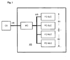
- Fig. 1 the memory system MS is shown with the memory controller MC, which is connected via a host bus HB to the controlling computer system CS.
- the flash chips FC which form the data memory.
- FC-SLC SLC chips FC-SLC associated with the first area B1
- FC-MLC MLC chips FC-MLC with the second area.
- the SLC chips FC-SLC have a much higher maximum extinguishing capability compared to the MLC chips FC-MLC.
- Fig. 2 the address table AT and the flash memory FS are shown with the two areas B1 and B2.
- the predetermined by the computer system logical block address LBA is converted into an associated physical block address PBA.
- the logical block address LBA serves as an index in the address table AT.
- the flash memory FS consists of 500 blocks with the physical block addresses PBA from 0 to 499.
- the first area B1 contains 100 blocks of the type SLC and the second area B2 contains 400 blocks of the type MLC.
- each area buffer blocks BB1, BB2 are provided for the write operations.
- the logical block address 50 initially points to the block 150 in the MLC area, while the logical block address 250 is assigned to the block 70 in the SLC area.
- a write to the logical block address 50 a block is now searched in the SLC area, which has a low value of Has a deletion counter. This is the block 70 associated with the logical block address 250.
- the physical block addresses of the addresses in the address table AT are exchanged. Now, the logical block address 50 points to the block 70 in the SLC area and the logical block address 250 to the block 150.
- Fig. 3 shows the structure of a physical block PB. It is divided into the sectors S1 to Sm, which respectively contain the payload area UD, a parity word CRC and the error correction word ECC.
- the block management table containing the clear counter EC and the wear level class WLC.
- the wear level class WLC can also be formed from the upper part of the clearing counter EC.
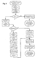
- Fig. 4 is the wear-leveling method of the memory shown.
- the logical block address LBA (X) points to the physical PBA (X) in the SLC area.
- a buffer block A is searched for and deleted.
- the deletion counter EC is increased. If the erase counter of A does not exceed the wear level threshold T1, block A is used as the buffer block and the logical block address (X) is assigned to block A. If the delete counter of A now exceeds the threshold T1 for the increase of the WearLevel class, this is increased and the clear counter is reset.
- a further block B in the SLC area is sought, namely the one with the smallest deletion counter.
- the logical block address LBA (A) is assigned to the block B and this is used as a buffer block.
- the logical block address LBA (X) is assigned to block B.
- the logical block address LBA (A) is assigned to the block B and this is used as a buffer block.
- the logical block address LBA (X) is now also assigned to block B.
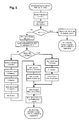
- Fig. 5 there is a write request for the logical block address LBA (X) in the SLC area.
- a buffer block A is sought, this cleared and increased its clear counter EC. If the erase counter of A does not exceed the wear level threshold T1, block A is used as the buffer block and the logical block address (X) is assigned to block A.
- the contents of the block B are copied to the deleted block A, and block B is deleted.
- the logical block address LBA (A) is assigned to the block B and this is used as a buffer block.
- the logical block address LBA (X) is assigned to block B.
- a free buffer block C is searched in the MLC flash chips with a low wear-level class.
- the content of block C is copied to A and then block C is deleted.
- the content of block B is copied to C and block B is deleted.
- the logical block address LBA (B) is assigned to the block C and the logical block address LBA (C) to the deleted block A.
- the logical block address LBA (A) is assigned to the block B and this is used as a buffer block.
- the logical block address LBA (X) is now also assigned to block B.
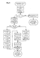
- Fig. 6 is the same wear-leveling method as in Fig. 5 with a shift of a block C from the MLC area into the SLC area. There is a write request for a block in the MLC area. If the buffer block B from the MLC area has a wear level class greater than the threshold ATBu for the shift from the MLC area to the SLC area, its content is shifted to the SLC area. The process steps, applied only to the other area, are otherwise the same as for Fig. 5 described.
- Fig. 7 is shown how a near reaching the maximum lifetime of the storage system is detected and output as a warning message.
- the wear level class WLC is increased, it is checked in which area the block is located. If it is in the SLC report, the wear level class WLC is compared with an SLC threshold T3. If the value is higher than the threshold T3, a warning message is issued. This can be done about the well-known in hard drives SMART method.
- the wear level class WLC is compared with an MLC threshold T4. If the value is higher than the threshold T4, a warning message is also issued.
Landscapes
- Engineering & Computer Science (AREA)
- Theoretical Computer Science (AREA)
- Physics & Mathematics (AREA)
- General Engineering & Computer Science (AREA)
- General Physics & Mathematics (AREA)
- Techniques For Improving Reliability Of Storages (AREA)
- Memory System (AREA)
- Read Only Memory (AREA)
Description
- Die Erfindung betrifft ein Verfahren zur Verwaltung eines Speichers mit mehreren Flashchips, die in eine Vielzahl von separat löschbaren physikalischen Blöcken gegliedert sind und diese Blöcke eine begrenzte maximale Löschhäufigkeit besitzen, und die Blöcke des Speichers über logische Blockadressen adressiert werden, die über eine Adresstabelle in physikalische Blockadressen umgesetzt werden, und in jedem Block ein Löschzähler mitgeführt wird.
- Speichersysteme, die aus Flashchips aufgebaut sind, insbesondere sogenannte Solid State Disks, gewinnen immer mehr an Bedeutung und es besteht die Notwendigkeit, solche preiswert anbieten zu können.
- Bei den Flashchips werden zwei unterschiedliche Typen verwendet. Die Single-Level-Cell-Chips SLC bieten eine hohe Anzahl von möglichen Schreib/Löschzyklen, sind aber relativ teuer. Die Multi-Level-Cell-Chips MLC sind wesentlich preiswerter, bieten aber nur eine deutlich geringere Anzahl von möglichen Schreib/Löschzyklen.
- Die Flashchips sind in eine Vielzahl von realen Blöcken organisiert, die separat gelöscht werden können. Die Blöcke werden vom Computersystem über logische Blockadressen adressiert.
- Beim Einsatz eines Speichers in einem Computersystem werden einige Daten häufig geändert, während andere Daten, wie etwa Applikationsprogramme, nur sehr selten überschrieben werden. Es ist nun wünschenswert, die selten geänderten Daten in den preiswerten Flashchips zu speichern und die teuren Flashchips nur für die häufig geänderten Daten vorzuhalten.
- In Flashspeichern werden Wear-Leveling-Verfahren eingesetzt, um eine gleichmäßige Verteilung der notwendigen Schreib/Löschzyklen auf alle Blöcke zu erreichen und somit die Lebensdauer des Speichers zu maximieren.
- Dazu wird über eine Adresstabelle eine Umsetzung von logischen Blockadressen in physikalische Blockadressen vorgenommen und diese Zuordnung entsprechend der Löschhäufigkeit der Blöcke verändert.
- In der Patentanmeldung
US2008/0209112A1 ist ein Speichersystem mit SLC- und MLC-Speicherchips beschrieben, bei dem vorrangig die SLC-Speicherchips genutzt werden. Wenn alle SLC-Speicherchips beschrieben sind, wird ein wenig genutzter SLC-Speicherblock in den MLC-Bereich kopiert, gelöscht und für neue Daten genutzt. Ein weitergehendes Wear-Leveling-Verfahren wird nicht genutzt. - Es ist die Aufgabe der Erfindung, ein Verfahren zu offenbaren, das es erlaubt, in einem Speicher zwei Typen von Flashchips mit unterschiedlich maximal möglichen Schreib/Löschzyklen zu kombinieren und dabei eine maximale Lebensdauer des Speichers zu erreichen.
- Diese Aufgabe wird durch die Merkmale des Anspruchs 1 gelöst. Vorteilhafte Ausgestaltungen des Verfahrens sind in den Unteransprüchen beschrieben.
- Das Speichersystem enthält einen Speichercontroller mit einer Firmware, in der das Verfahren durchgeführt wird. Alle Flashchips des Speichers sind an den Controller angeschlossen und werden von diesem verwaltet. Der Speicher ist erfindungsgemäß in zwei Bereiche geteilt, wovon der erste Bereich mit den Single-Level-Cell-Chips SLC ausgestattet ist, während der zweite Bereich die Multi-Level-Cell-Chips MLC enthält. Typischerweise beträgt die Größe des zweiten Bereiches ein Vielfaches des ersten Bereiches, es sind aber alle Größenverhältnisse möglich. Die Größen der separat löschbaren realen Blöcke können in den beiden Flashtypen unterschiedlich sein. Um das Verfahren in beiden Bereichen auf die gleiche Weise durchführen zu können, werden von der Firmware physikalische Blöcke gebildet, die eine feste Größe besitzen und in den beiden Bereichen aus unterschiedlich vielen realen Blöcken bestehen können.
- In der Adressumsetzungstabelle ist zu jeder logischen Blockadresse eine physikalische Blockadresse eines Speicherblockes zugeordnet. Das übergeordnete Computersystem benutzt die logischen Blockadressen vollständig wahlfrei.
- Das Verfahren sieht in einer Startphase vor, dass, wenn über die logische Blockadresse eine physikalische Adresse im zweiten Bereich angesprochen wird, dieser logischen Blockadresse nun in der Adresstabelle eine physikalische Blockadresse eines freien Speicherblocks aus dem ersten Bereich zugeordnet wird. Damit füllt sich der erste Bereich in der Startphase.
- Jedem Block ist ein Löschzähler zugeordnet, der bei jedem Schreib/Löschzyklus erhöht wird. Wenn nun im ersten Bereich kein freier Block mehr vorhanden ist und ein weiterer Schreibvorgang auszuführen ist, wird ein Block mit dem niedrigsten Wert des Löschzählers im ersten Bereich gesucht und dieser in den zweiten Bereich kopiert. Die physikalischen Blockadressen zu den zugeordneten logischen Blockadressen dieser Blöcke in der Adresstabelle werden getauscht. Der Block im ersten Bereich wird gelöscht und mit den neuen Daten beschrieben.
- Wenn alle Blöcke des ersten oder zweiten Bereiches gefüllt sind, wird in den NormalBetrieb der Speicherverwaltung übergegangen. Mit einem Wear-Leveling-Verfahren werden die Bereiche des Speichers entsprechend ihrer zulässigen Löschhäufigkeit gleichmäßig beansprucht und die Lebensdauer aller Flashchips des gesamten Speichers wird maximal ausgenutzt.
- Für das Wear-Leveling-Verfahren werden in beiden Bereichen gelöschte Pufferblöcke vorgehalten, in die neue Daten für bereits beschriebene Blöcke eingeschrieben werden. Nach dem vollständigen Beschreiben des Pufferblockes wird seine physikalische Adresse anstelle des bisher adressierten physikalischen Blockes zu der benutzten logischen Blockadresse in die Adresstabelle eingetragen und der letztere gelöscht. Dabei wird dann sein Löschzähler erhöht.
- Für die Bereiche wird jeweils eine Wear-Level-Schwelle definiert, die im ersten Bereich höher liegt und im zweiten Bereich niedriger liegt. Weiterhin wird für jeden Block ein Wear-Level-Class-Zähler mitgeführt. Der Löschzähler wird bei seiner Erhöhung daraufhin überprüft, ob sein Wert die für diesen Block gültige Wear-Level-Schwelle erreicht hat. Ist dies der Fall, wird der Wear-Level-Class-Zähler erhöht und der Löschzähler auf den Wert 0 zurückgestellt. Bei der Suche nach einem neuen Pufferblock für das erneute Beschreiben eines Blockes wird in dem gleichen Bereich des Speichers ein solcher Block gewählt, der einen niedrigen Wert seines Wear-Level-Class-Zählers aufweist. Auf diese Weise wird eine gleichmäßige Löschhäufigkeit der Blöcke innerhalb eines Bereiches erreicht.
- Falls ein Block innerhalb des ersten Bereiches einen niedrigen Wert seines Wear-Level-Class-Zählers aufweist oder ein Block innerhalb des zweiten Bereiches einen hohen Wert seines Wear-Level-Class-Zählers aufweist, kann sein Inhalt in den jeweils anderen Bereich verschoben werden. Dazu werden eine Abwärtsschwelle, die den höchsten aktuellen Wert der Wear-Level-Class-Zähler im zweiten Bereich angibt, und eine Aufwärtsschwelle, die den niedrigsten aktuellen Wert der Wear-Level-Class-Zähler im ersten Bereich angibt, bestimmt. Wenn nun bei einer Erhöhung des Wear-Level-Class-Zählers im ersten Bereich ein Wert unterhalb der Abwärtsschwelle vorliegt, wird ein Pufferblock im zweiten Bereich gesucht. Ebenso wird bei einer Erhöhung des Wear-Level-Class-Zählers im zweiten Bereich ein Wert oberhalb der Aufwärtsschwelle erreicht, wird ein Pufferblock im ersten Bereich gesucht. Auf diese Weise wird eine an die Charakteristik der verwendeten Typen von Flashchips orientierte Löschhäufigkeit der Blöcke innerhalb des gesamten Speichers erreicht. Die Lebensdauer aller Flashchips des gesamten Speichers wird maximal ausgenutzt.
- In dem beschriebenen Verfahren wird auch die verbliebene Zuverlässigkeit der Flashchips überprüft. Dazu wird beim Schreiben von Daten über die Daten ein Fehlerkorrekturwort gebildet und mit in dem Block abgespeichert wird, sowie über den Inhalt des Blockes ein Paritätswort gebildet und abgespeichert. Wenn nun einer oder mehrere Fehler beim Lesen der Daten erkannt werden, werden diese mittels des Fehlerkorrekturwortes korrigiert und mittels des Paritätswortes noch einmal überprüft. Wenn nun die Fehleranzahl in der Nähe der Fehlerkorrekturmöglichkeiten des Speichersystems (z.B. vier oder mehr Bitfehler bei einer Korrekturfähigkeit des Speichers von 6 Bitfehlern) liegt, ist dies ein Zeichen für die nachlassende Zuverlässigkeit des Speichers und es wird eine ,außerordentliche' Wearlevelprozedur auf dem Block durchgeführt bzw. der Block wird für eine solche Wearlevelprozedur vorgemerkt, falls der Block gerade zum Schreiben geöffnet ist. Die Vormerkung wird abgehandelt, sobald der Block geschlossen wird. Dabei werden dann die Daten, die aktuell mit korrigierbaren Mehrbitfehlern abgespeichert sind, in einen anderen, noch am seltensten gelöschten Block umkopiert und somit einem Refresh unterzogen. Damit werden insbesondere solche Lesefehler vermieden, die umgebungs- und datenabhängig sind.
- Weiterhin sind für den ersten und den zweiten Bereich des Blockes maximal zulässige Löschungen des Speichers vorgegeben. Erreicht nun bei einer Erhöhung eines Wear-Level-Class-Zählers deren aktueller Wert den vorgegebenen Maximal-Wert wird eine Warnmeldung ausgegeben. Diese kann von dem Computersystem mit bekannten Verfahren ausgewertet werden.
- Ausführungsformen der Erfindung sind in den Figuren beispielhaft beschrieben.
-
Fig. 1 zeigt ein Blockdiagramm eines Flashspeichersystems. -
Fig. 2 zeigt die Adresszuordnung zu den Bereichen im Flashspeicher. -
Fig. 3 zeigt den Aufbau eines physikalischen Blockes. -
Fig. 4 zeigt das Wear-Levelling im Speicher. -
Fig. 5 zeigt das Wear-Levelling mit Verschiebung eines Blockes in den MLC-Bereich. -
Fig. 6 zeigt das Wear-Levelling mit Verschiebung eines Blockes in den SLC-Bereich. -
Fig. 7 zeigt die Ausgabe einer Warnmeldung beim nahen Erreichen der maximalen Lebensdauer. - In
Fig. 1 ist das Speichersystem MS mit dem Speichercontroller MC gezeigt, der über einen Hostbus HB mit dem steuernden Computersystem CS verbunden ist. An dem Speichercontroller MC sind über den Speicherbus MB die Flashchips FC, die den Datenspeicher bilden. Es sind zwei Typen von Flashchips FC vorhanden, wobei die SLC-Chips FC-SLC dem ersten Bereich B1 und die MLC-Chips FC-MLC dem zweiten Bereich zugeordnet sind. Die SLC-Chips FC-SLC weisen gegenüber den MLC-Chips FC-MLC eine wesentlich höhere maximale Löschmöglichkeit auf. - In
Fig. 2 ist die Adresstabelle AT und der Flashspeicher FS mit den beiden Bereichen B1 und B2 dargestellt. Die vom Computersystem vorgegebene logische Blockadresse LBA wird in eine zugehörige physikalische Blockadresse PBA umgesetzt. Dabei dient die logische Blockadresse LBA als Index in die Adresstabelle AT. - In dem hier gezeigten Beispiel besteht der Flashspeicher FS aus 500 Blöcken mit den physikalischen Blockadressen PBA von 0 bis 499. Dabei enthält der erste Bereich B1 100 Blöcke vom Typ SLC und der zweite Bereich B2 400 Blöcke vom Typ MLC. In jedem Bereich sind für die Schreiboperationen Pufferblöcke BB1, BB2 vorgesehen.
- In dem hier gezeigten Beispiel weist die logische Blockadresse 50 zunächst auf den Block 150 im MLC-Bereich, während der logischen Blockadresse 250 der Block 70 im SLC-Bereich zugeordnet ist. Bei einem Schreibvorgang auf die logische Blockadresse 50 wird nun ein Block im SLC-Bereich gesucht, der einen niedrigen Wert des Löschzählers besitzt. Dies sei der Block 70, der der logischen Blockadresse 250 zugeordnet ist. Damit nun der Schreibvorgang in den SLC-Bereich hinein erfolgt, werden die physikalischen Blockadressen der in der Adresstabelle AT getauscht. Nun zeigt die logische Blockadresse 50 auf den Block 70 im SLC-Bereich und die logische Blockadresse 250 auf den Block 150.
-
Fig. 3 zeigt den Aufbau eines physikalischen Blockes PB. Er ist in die Sektoren S1 bis Sm gegliedert, die jeweils den Nutzdatenbereich UD, ein Paritätswort CRC und das Fehlerkorrekturwort ECC enthalten. Daneben gibt es für jeden physikalischen Block PB einen Eintrag in der Blockmanagementtabelle, der den Löschzähler EC und die Angabe der Wear-Level-Class WLC enthält. Die Wear-Level-Class WLC kann auch aus dem oberen Teil des Löschzählers EC gebildet sein. - In
Fig. 4 ist das Wear-Leveling-Verfahren des Speichers dargestellt. Bei einem Schreibauftrag für den logischen Block X weist die logische Blockadresse LBA (X) auf die physikalische PBA (X) im SLC-Bereich. Dort wird ein Pufferblock A gesucht und dieser gelöscht. Dabei wird der Löschzähler EC erhöht. Wenn der Löschzähler von A die Schwelle T1 für die Erhöhung der WearLevel-Class nicht überschreitet, wird Block A als Pufferblock genutzt und die logische Blockadresse (X) dem Block A zugeordnet. Wenn der Löschzähler von A nun die Schwelle T1 für die Erhöhung der WearLevel-Class überschreitet, wird diese erhöht und der Löschzähler zurückgesetzt. Es wird ein weiterer Block B im SLC- Bereich gesucht, und zwar derjenige mit dem kleinsten Löschzähler. - In der Startphase wird nun der Inhalt von B in den gerade gelöschten Block A kopiert und B gelöscht. Ohne Beschränkung der Allgemeinheit darf hier vorausgesetzt werden, dass dieses Löschen hier nicht zur Erhöhung der Wear-Level-Class führt.
- Die logische Blockadresse LBA (A) wird dem Block B zugeordnet und dieser als Pufferblock genutzt. Am Ende des Schreibvorganges ist die logische Blockadresse LBA (X) dem Block B zugeordnet.
- In der Startphase werden alle SLC-Flashchips beschrieben. Nach der Startphase wird bei der Erhöhung der Wear-Level-Class ein freier Pufferblock C in den MLC-Flashchips mit einem niedrigen Wert der Wear-level-Class gesucht. Dieser Block C wird gelöscht, der Inhalt des Blockes B hineinkopiert und die logische Blockadresse LBA (B) dem Block C zugeordnet. Die logische Blockadresse LBA (C) wird dem gelöschten Block A zugeordnet. Der Block B wird nun auch gelöscht.
- Die logische Blockadresse LBA (A) wird dem Block B zugeordnet und dieser als Pufferblock genutzt. Am Ende des Schreibvorganges ist nun auch die logische Blockadresse LBA (X) dem Block B zugeordnet.
- In
Fig. 5 und6 sind die Wear-Level-Verfahren mit einer Verschiebung des zu schreibenden Blockes in den jeweils anderen Bereich dargestellt. Der Beginn des Schreibvorgangs entspricht dem Verfahren gemäßFig. 4 . - In
Fig. 5 liegt ein Schreibauftrag für die logische Blockadresse LBA (X) im SLC-Bereich vor. Dort wird ein Bufferblock A gesucht, dieser gelöscht und sein Löschzähler EC erhöht. Wenn der Löschzähler von A die Schwelle T1 für die Erhöhung der WearLevel-Class nicht überschreitet, wird Block A als Pufferblock genutzt und die logische Blockadresse (X) dem Block A zugeordnet. - Wenn der Löschzähler von A nun die Schwelle T1 für die Erhöhung der WearLevel-Class überschreitet, wird diese erhöht und der Löschzähler zurückgesetzt. Es wird ein weiterer Block B im SLC- Bereich gesucht.
- Nun wird überprüft, ob die Wear-Level-Class des Blockes B kleiner ist als eine vorgegebene Schwelle ATBd, die eine Verschiebung von Blöcken aus dem SLC-Bereich in den MLC-Bereich bewirkt.
- Wenn diese Schwelle nicht unterschritten ist, wird der Inhalt des Blocks B in den gelöschten Block A kopiert, und Block B gelöscht. Die logische Blockadresse LBA (A) wird dem Block B zugeordnet und dieser als Pufferblock genutzt. Am Ende des Schreibvorganges ist die logische Blockadresse LBA (X) dem Block B zugeordnet.
- Wenn die Schwelle ATBd unterschritten ist, wird ein freier Pufferblock C in den MLC-Flashchips mit einem niedrigen Wert der Wear-level-Class gesucht. Der Inhalt des Blockes C wird nach A kopiert und dann Block C gelöscht. Der Inhalt des Blockes B wird nach C kopiert und Block B gelöscht. Die logische Blockadresse LBA (B) wird dem Block C und die logische Blockadresse LBA (C) dem gelöschten Block A zugeordnet.
- Die logische Blockadresse LBA (A) wird dem Block B zugeordnet und dieser als Pufferblock genutzt. Am Ende des Schreibvorganges ist nun auch die logische Blockadresse LBA (X) dem Block B zugeordnet.
- In
Fig. 6 ist das gleiche Wear-Leveling-Verfahren wie inFig. 5 mit einer Verschiebung eines Blockes C aus dem MLC-Bereich in den SLC-Bereich dargestellt. Es liegt ein Schreibauftrag für einen Block im MLC-Bereich vor. Wenn der Pufferblock B aus dem MLC-Bereich eine Wear-Level-Class größer als die Schwelle ATBu für die Verschiebung aus dem MLC-Bereich in den SLC-Bereich besitzt, wird sein Inhalt in den SLC-Bereich verschoben. Die Verfahrensschritte, nur angewendet auf den anderen Bereich, sind ansonsten die gleichen wie fürFig. 5 beschrieben. - In
Fig. 7 ist dargestellt, wie ein nahes Erreichen der maximalen Lebensdauer des Speichersystems erkannt und als Warnmeldung ausgegeben wird. - Wenn beim Löschen eines Blockes X die Wear-Level-Class WLC erhöht wird, wird überprüft, in welchem Bereich sich der Block befindet. Befindet er sich im SLC-Berich wird die Wear-Level-Class WLC mit einer SLC-Schwelle T3 verglichen. Ist der Wert höher als die Schwelle T3 wird eine Warnmeldung ausgegeben. Dies kann etwa etwa nach dem bei Festplatten bekannten SMART-Verfahren erfolgen.
- Befindet sich der Block X im MLC-Berich wird die Wear-Level-Class WLC mit einer MLC-Schwelle T4 verglichen. Ist der Wert höher als die Schwelle T4 wird ebenso eine Warnmeldung ausgegeben.
- Somit kann auf einfache Weise das nahe Erreichen der maximalen Lebensdauer des Speichersystems vom Anwender bemerkt werden.
-
- A, B, C, X
- Physikalische Blöcke
- AT
- Adresstabelle
- ATBu,
- Schwelle für Bereichswechsel in den SLC-Bereich
- ATBd
- Schwelle für Bereichswechsel in den MLC-Bereich
- B1
- erster Bereich
- B2
- zweiter Bereich
- BB1
- Pufferblöcke im ersten Bereich
- BB2
- Pufferblöcke im zweiten Bereich
- BEF
- Löschhäufigkeit des Blockes
- CRC
- Paritätswort
- CS
- Computersystem
- EC
- Löschzähler
- ECC
- Fehlerkorrekturwort
- FC
- Flashchip
- FS
- Flashspeicher
- HB
- Hostbus
- LBA
- Logische Blockadresse
- MB
- Speicherbus
- MC
- Speichercontroller
- MLC
- Multi-Level-Cell-Speicher
- MS
- Speichersystem
- m
- Anzahl Sektoren
- n
- Anzahl logische Blockadressen
- PB
- Physikalischer Block
- PBA
- Physikalische Blockadresse
- SLC
- Single-Level-Cell-Speicher
- Sl, Sm
- Sektoren im Block
- T1...T4
- Schwellen für Löschzähler
- UD
- Nutzdaten
- WLC
- Wear-Level-Class
Claims (11)
- Verfahren zur Verwaltung eines Flashspeichers mit mehreren Flashchips, die in eine Vielzahl von separat löschbaren physikalischen Blöcken gegliedert sind und diese Blöcke eine begrenzte maximale Löschhäufigkeit besitzen, und die Blöcke des Speichers über logische Blockadressen (LBA) adressiert werden, die über eine Adresstabelle (AT) in physikalische Blockadressen umgesetzt werden, und in jedem Block ein Löschzähler mitgeführt wird, in dem die Anzahl der Löschungen des Blockes gezählt wird, wobei
in dem Flashspeicher (FS) zwei Bereiche mit unterschiedlichen Typen von Flashchips vorhanden sind, wobei der erste Bereich (B1) Single-Level-Flashchips mit einer sehr großen maximalen Löschhäufigkeit enthält und der zweite Bereich (B2) Multi-Level-Flashchips mit einer niedrigeren maximalen Löschhäufigkeit enthält, und dass- beim Beschreiben des Speichers die Adressumsetzung der logischen Adressen in physikalische Adressen zunächst so erfolgt, dass alle Blöcke des ersten Bereiches (B1) beschrieben werden,- wenn alle Blöcke des ersten Bereiches beschrieben sind und ein weiterer Schreibvorgang auszuführen ist, der Block in dem ersten Bereich (B1) mit dem niedrigsten Löschzähler in einen unbeschriebenen Block im zweiten Bereich kopiert wird,- in der Adresstabelle (AT) die physikalischen Blockadressen zu den zugeordneten logischen Blockadressen (LBA) dieser Blöcke getauscht werden,- der Block im ersten Bereich gelöscht wird, und- dieser Block mit den neuen Daten beschrieben wird, dadurch gekennzeichnet, dassfür jeden Bereich eine Wear-Level-Schwelle (T1, T2) definiert wird und zu jedem Block ein Wear-Level-Class-Zähler (WLC) geführt wird, der bei einem Erreichen der für diesen Block gültigen Wear-Level-Schwelle des Löschzählers (EC) erhöht wird und der Löschzähler auf 0 gesetzt wird. - Verfahren nach Anspruch 1, dadurch gekennzeichnet, dass
in beiden Bereichen gelöschte Pufferblöcke (BB1, BB2) vorgehalten werden, in die neue Daten für bereits beschriebene Blöcke eingeschrieben werden. - Verfahren nach Anspruch 2, dadurch gekennzeichnet, dass
nach dem Schreiben von neuen Daten eines Blockes in einen Pufferblock die physikalische Adresse dieses Blockes zu der logischen Blockadresse in die Adresstabelle (AT) eingetragen wird, der bisherige Block gelöscht wird und sein Löschzähler (EC) erhöht wird. - Verfahren nach Anspruch 1, dadurch gekennzeichnet, dass
bei einer Suche nach einem Pufferblock nach einem gelöschten Block mit einem niedrigen Wert des Wear-Level-Class-Zählers in dem gleichen Bereich des Speichers gesucht wird. - Verfahren nach Anspruch 1, dadurch gekennzeichnet, dass
für den Übergang vom ersten Bereich in den zweiten Bereich eine Abwärtsschwelle (ATBu) und für den Übergang vom zweiten Bereich zum ersten Bereich eine Aufwärtsschwelle (ATBd) definiert ist. - Verfahren nach Anspruch 5, dadurch gekennzeichnet, dass
für den ersten Bereich die Abwärtsschwelle (ATBd) der höchste aktuelle Wert der Wear-Level-Class-Zähler (WLC) im zweiten Bereich ermittelt wird, und dass für den zweiten Bereich die Aufwärtsschwelle (ATBu) der niedrigste aktuelle Wert der Wear-Level-Class-Zähler im ersten Bereich ermittelt wird. - Verfahren nach Anspruch 5, dadurch gekennzeichnet, dass
bei einer Erhöhung des Wear-Level-Class-Zählers (WLC) im ersten Bereich ein Unterschreiten der Abwärtsschwelle (ATBd) überprüft wird und falls diese unterschritten ist, ein Pufferblock im zweiten Bereich genutzt wird. - Verfahren nach Anspruch 5, dadurch gekennzeichnet, dass
bei einer Erhöhung des Wear-Level-Class-Zählers (WLC) im zweiten Bereich ein Überschreiten der Aufwärtsschwelle (ATBu) überprüft wird und falls diese überschritten wird, ein Pufferblock im ersten Bereich genutzt wird. - Verfahren nach Anspruch 1, dadurch gekennzeichnet, dass
beim Schreiben von Daten über die Daten ein Fehlerkorrekturwort (ECC) gebildet und mit in dem Block abgespeichert wird, sowie über den Inhalt des Blockes eine Paritätswort (CRC) gebildet und abgespeichert wird. - Verfahren nach Anspruch 9, dadurch gekennzeichnet, dass
bei einem Auftreten mehrerer Fehler beim Lesen aus einem Block unmittelbar eine Wearlevelprozedur für diesen Block durchgeführt wird. - Verfahren nach Anspruch 1, dadurch gekennzeichnet, dass
für den ersten und den zweiten Bereich die jeweils maximal zulässigen Löschungen von Blöcken vorgegeben sind und bei einer Erhöhung der Wear-Level-Class-Zähler deren aktueller Wert mit den vorgegebenen Werten (T3, T4) verglichen wird und bei einem Erreichen der maximal zulässigen Löschungen eine Warnmeldung ausgegeben wird.
Applications Claiming Priority (1)
| Application Number | Priority Date | Filing Date | Title |
|---|---|---|---|
| PCT/DE2009/075011 WO2010097065A1 (de) | 2009-02-26 | 2009-02-26 | Verfahren zur verwaltung von flashspeichern mit gemischten speichertypen |
Publications (2)
| Publication Number | Publication Date |
|---|---|
| EP2401680A1 EP2401680A1 (de) | 2012-01-04 |
| EP2401680B1 true EP2401680B1 (de) | 2013-11-06 |
Family
ID=41100719
Family Applications (1)
| Application Number | Title | Priority Date | Filing Date |
|---|---|---|---|
| EP09776141.5A Not-in-force EP2401680B1 (de) | 2009-02-26 | 2009-02-26 | Verfahren zur verwaltung von flashspeichern mit gemischten speichertypen |
Country Status (3)
| Country | Link |
|---|---|
| US (1) | US8706998B2 (de) |
| EP (1) | EP2401680B1 (de) |
| WO (1) | WO2010097065A1 (de) |
Cited By (1)
| Publication number | Priority date | Publication date | Assignee | Title |
|---|---|---|---|---|
| DE102014101185A1 (de) | 2014-01-31 | 2015-08-06 | Hyperstone Gmbh | Verfahren zur Verwaltung von Flash-Speichern mit gemischten Speichertypen unter Verwendung einer fein-granulierten Zuordnung logischer auf physikalische Speicheradressen |
Families Citing this family (14)
| Publication number | Priority date | Publication date | Assignee | Title |
|---|---|---|---|---|
| CN101751446A (zh) * | 2008-12-17 | 2010-06-23 | 深圳富泰宏精密工业有限公司 | 快闪存储器文件管理系统及方法 |
| KR20100107089A (ko) * | 2009-03-25 | 2010-10-05 | 삼성전자주식회사 | 저장 장치 및 이를 포함하는 데이터 저장 시스템 |
| GB2490991B (en) * | 2011-05-19 | 2017-08-30 | Ibm | Wear leveling |
| US9158621B2 (en) * | 2011-08-29 | 2015-10-13 | Sandisk Technologies Inc. | System and method of copying data |
| US9208070B2 (en) | 2011-12-20 | 2015-12-08 | Sandisk Technologies Inc. | Wear leveling of multiple memory devices |
| US9262336B2 (en) | 2011-12-23 | 2016-02-16 | Intel Corporation | Page miss handler including wear leveling logic |
| WO2013095641A1 (en) * | 2011-12-23 | 2013-06-27 | Intel Corporation | Sub-block based wear leveling |
| US9117533B2 (en) | 2013-03-13 | 2015-08-25 | Sandisk Technologies Inc. | Tracking erase operations to regions of non-volatile memory |
| US9153331B2 (en) | 2013-03-13 | 2015-10-06 | Sandisk Technologies Inc. | Tracking cell erase counts of non-volatile memory |
| US10042750B2 (en) | 2013-03-15 | 2018-08-07 | Micron Technology, Inc. | Apparatuses and methods for adaptive control of memory using an adaptive memory controller with a memory management hypervisor |
| US9477546B2 (en) * | 2013-06-21 | 2016-10-25 | Marvell World Trade Ltd. | Methods and apparatus for optimizing lifespan of a storage device |
| TWI653632B (zh) * | 2017-09-29 | 2019-03-11 | 群聯電子股份有限公司 | 記憶體管理方法、記憶體控制電路單元及記憶體儲存裝置 |
| CN109669620B (zh) * | 2017-10-13 | 2021-11-30 | 群联电子股份有限公司 | 存储器管理方法、存储器控制电路单元及存储器储存装置 |
| US10860219B2 (en) | 2018-10-05 | 2020-12-08 | Micron Technology, Inc. | Performing hybrid wear leveling operations based on a sub-total write counter |
Family Cites Families (5)
| Publication number | Priority date | Publication date | Assignee | Title |
|---|---|---|---|---|
| US7660941B2 (en) * | 2003-09-10 | 2010-02-09 | Super Talent Electronics, Inc. | Two-level RAM lookup table for block and page allocation and wear-leveling in limited-write flash-memories |
| US8078794B2 (en) * | 2000-01-06 | 2011-12-13 | Super Talent Electronics, Inc. | Hybrid SSD using a combination of SLC and MLC flash memory arrays |
| US7953931B2 (en) | 1999-08-04 | 2011-05-31 | Super Talent Electronics, Inc. | High endurance non-volatile memory devices |
| US7752382B2 (en) * | 2005-09-09 | 2010-07-06 | Sandisk Il Ltd | Flash memory storage system and method |
| US20080140918A1 (en) * | 2006-12-11 | 2008-06-12 | Pantas Sutardja | Hybrid non-volatile solid state memory system |
-
2009
- 2009-02-26 US US13/202,332 patent/US8706998B2/en not_active Expired - Fee Related
- 2009-02-26 WO PCT/DE2009/075011 patent/WO2010097065A1/de not_active Ceased
- 2009-02-26 EP EP09776141.5A patent/EP2401680B1/de not_active Not-in-force
Cited By (1)
| Publication number | Priority date | Publication date | Assignee | Title |
|---|---|---|---|---|
| DE102014101185A1 (de) | 2014-01-31 | 2015-08-06 | Hyperstone Gmbh | Verfahren zur Verwaltung von Flash-Speichern mit gemischten Speichertypen unter Verwendung einer fein-granulierten Zuordnung logischer auf physikalische Speicheradressen |
Also Published As
| Publication number | Publication date |
|---|---|
| US20110302359A1 (en) | 2011-12-08 |
| US8706998B2 (en) | 2014-04-22 |
| WO2010097065A1 (de) | 2010-09-02 |
| EP2401680A1 (de) | 2012-01-04 |
Similar Documents
| Publication | Publication Date | Title |
|---|---|---|
| WO2010097065A1 (de) | Verfahren zur verwaltung von flashspeichern mit gemischten speichertypen | |
| DE102020107659A1 (de) | Zonenbildung für gezonte namensräume | |
| DE112020002792B4 (de) | Verschleissorientierte blockmodusumwandlung in nichtflüchtigen speichern | |
| DE112020000139T5 (de) | Nicht sequentiell in zonen aufgeteilte namensräume | |
| DE102017120840B4 (de) | Verfahren und Vorrichtung zur Detektion und Handhabung von Lesestörungen | |
| DE69227499T2 (de) | Einen Flashspeicher verwendendes Speichergerät | |
| DE69431795T2 (de) | Massenspeicherarchitektur mit flash-speicher | |
| DE69414556T2 (de) | Schnell loeschbare datei | |
| DE69612752T2 (de) | Speicheranordnung | |
| DE602004011097T2 (de) | Flash-speicherdatenkorrektur- und scrub-techniken | |
| DE102008057219B4 (de) | Verfahren zum Betreiben eines Solid-State-Speichersystems, Solid-State-Speichersystem und Computersystem | |
| DE102008003944B4 (de) | Speichersystem und Programmierverfahren für ein Speichersystem | |
| DE60319407T2 (de) | Verfolgen der am häufigsten gelöschten blöcke eines nichtflüchtigen speichersystems | |
| DE102019123709A1 (de) | Verwendung verschachtelter schreibvorgänge zur trennung von die-ebenen | |
| DE102006005877A1 (de) | Adresszuordnungstabelle und Verfahren zum Erzeugen einer Adresszuordnungstabelle | |
| DE112020005695B4 (de) | Speichercontroller für solid-state-speichereinheiten | |
| DE112008001151B4 (de) | Mehrbitprogrammiervorrichtung und Verfahren zum Mehrbitprogrammieren | |
| DE102014101185A1 (de) | Verfahren zur Verwaltung von Flash-Speichern mit gemischten Speichertypen unter Verwendung einer fein-granulierten Zuordnung logischer auf physikalische Speicheradressen | |
| DE102012208141B4 (de) | Ausgleich nachlassender Funktionsfähigkeit | |
| DE102007016460A1 (de) | Nichtflüchtiges Speicherbauelement, nichtflüchtiges Speichersystem und Leseverfahren für ein nichtflüchtiges Speicherbauelement | |
| DE112008002553T5 (de) | Einsatz eines MLC-Flash als SLC durch Schreiben von Dummy-Daten | |
| DE112022004121T5 (de) | Superblockzuordnung über supervorrichtung in zns-ssd | |
| DE112022000468T5 (de) | Unterschiedliche schreibpriorisierung in zns-vorrichtungen | |
| EP2215636B1 (de) | VERFAHREN ZUR GLEICHMÄßIGEN NUTZUNG MEHRERER FLASHSPEICHERCHIPS | |
| DE112022000546T5 (de) | Schnelle speicherbereinigung in ssds mit gezonten namensräumen |
Legal Events
| Date | Code | Title | Description |
|---|---|---|---|
| PUAI | Public reference made under article 153(3) epc to a published international application that has entered the european phase |
Free format text: ORIGINAL CODE: 0009012 |
|
| 17P | Request for examination filed |
Effective date: 20110727 |
|
| AK | Designated contracting states |
Kind code of ref document: A1 Designated state(s): AT BE BG CH CY CZ DE DK EE ES FI FR GB GR HR HU IE IS IT LI LT LU LV MC MK MT NL NO PL PT RO SE SI SK TR |
|
| DAX | Request for extension of the european patent (deleted) | ||
| GRAP | Despatch of communication of intention to grant a patent |
Free format text: ORIGINAL CODE: EPIDOSNIGR1 |
|
| INTG | Intention to grant announced |
Effective date: 20130813 |
|
| GRAS | Grant fee paid |
Free format text: ORIGINAL CODE: EPIDOSNIGR3 |
|
| GRAA | (expected) grant |
Free format text: ORIGINAL CODE: 0009210 |
|
| AK | Designated contracting states |
Kind code of ref document: B1 Designated state(s): AT BE BG CH CY CZ DE DK EE ES FI FR GB GR HR HU IE IS IT LI LT LU LV MC MK MT NL NO PL PT RO SE SI SK TR |
|
| REG | Reference to a national code |
Ref country code: GB Ref legal event code: FG4D Free format text: NOT ENGLISH |
|
| REG | Reference to a national code |
Ref country code: CH Ref legal event code: EP |
|
| REG | Reference to a national code |
Ref country code: AT Ref legal event code: REF Ref document number: 639884 Country of ref document: AT Kind code of ref document: T Effective date: 20131215 |
|
| REG | Reference to a national code |
Ref country code: IE Ref legal event code: FG4D Free format text: LANGUAGE OF EP DOCUMENT: GERMAN |
|
| REG | Reference to a national code |
Ref country code: DE Ref legal event code: R096 Ref document number: 502009008300 Country of ref document: DE Effective date: 20140102 |
|
| REG | Reference to a national code |
Ref country code: NL Ref legal event code: VDEP Effective date: 20131106 |
|
| REG | Reference to a national code |
Ref country code: LT Ref legal event code: MG4D |
|
| PG25 | Lapsed in a contracting state [announced via postgrant information from national office to epo] |
Ref country code: LT Free format text: LAPSE BECAUSE OF FAILURE TO SUBMIT A TRANSLATION OF THE DESCRIPTION OR TO PAY THE FEE WITHIN THE PRESCRIBED TIME-LIMIT Effective date: 20131106 Ref country code: IS Free format text: LAPSE BECAUSE OF FAILURE TO SUBMIT A TRANSLATION OF THE DESCRIPTION OR TO PAY THE FEE WITHIN THE PRESCRIBED TIME-LIMIT Effective date: 20140306 Ref country code: HR Free format text: LAPSE BECAUSE OF FAILURE TO SUBMIT A TRANSLATION OF THE DESCRIPTION OR TO PAY THE FEE WITHIN THE PRESCRIBED TIME-LIMIT Effective date: 20131106 Ref country code: NO Free format text: LAPSE BECAUSE OF FAILURE TO SUBMIT A TRANSLATION OF THE DESCRIPTION OR TO PAY THE FEE WITHIN THE PRESCRIBED TIME-LIMIT Effective date: 20140206 Ref country code: FI Free format text: LAPSE BECAUSE OF FAILURE TO SUBMIT A TRANSLATION OF THE DESCRIPTION OR TO PAY THE FEE WITHIN THE PRESCRIBED TIME-LIMIT Effective date: 20131106 Ref country code: SE Free format text: LAPSE BECAUSE OF FAILURE TO SUBMIT A TRANSLATION OF THE DESCRIPTION OR TO PAY THE FEE WITHIN THE PRESCRIBED TIME-LIMIT Effective date: 20131106 Ref country code: NL Free format text: LAPSE BECAUSE OF FAILURE TO SUBMIT A TRANSLATION OF THE DESCRIPTION OR TO PAY THE FEE WITHIN THE PRESCRIBED TIME-LIMIT Effective date: 20131106 |
|
| PG25 | Lapsed in a contracting state [announced via postgrant information from national office to epo] |
Ref country code: LV Free format text: LAPSE BECAUSE OF FAILURE TO SUBMIT A TRANSLATION OF THE DESCRIPTION OR TO PAY THE FEE WITHIN THE PRESCRIBED TIME-LIMIT Effective date: 20131106 Ref country code: ES Free format text: LAPSE BECAUSE OF FAILURE TO SUBMIT A TRANSLATION OF THE DESCRIPTION OR TO PAY THE FEE WITHIN THE PRESCRIBED TIME-LIMIT Effective date: 20131106 |
|
| PG25 | Lapsed in a contracting state [announced via postgrant information from national office to epo] |
Ref country code: PT Free format text: LAPSE BECAUSE OF FAILURE TO SUBMIT A TRANSLATION OF THE DESCRIPTION OR TO PAY THE FEE WITHIN THE PRESCRIBED TIME-LIMIT Effective date: 20140306 |
|
| PG25 | Lapsed in a contracting state [announced via postgrant information from national office to epo] |
Ref country code: EE Free format text: LAPSE BECAUSE OF FAILURE TO SUBMIT A TRANSLATION OF THE DESCRIPTION OR TO PAY THE FEE WITHIN THE PRESCRIBED TIME-LIMIT Effective date: 20131106 |
|
| REG | Reference to a national code |
Ref country code: DE Ref legal event code: R097 Ref document number: 502009008300 Country of ref document: DE |
|
| PG25 | Lapsed in a contracting state [announced via postgrant information from national office to epo] |
Ref country code: RO Free format text: LAPSE BECAUSE OF FAILURE TO SUBMIT A TRANSLATION OF THE DESCRIPTION OR TO PAY THE FEE WITHIN THE PRESCRIBED TIME-LIMIT Effective date: 20131106 Ref country code: IT Free format text: LAPSE BECAUSE OF FAILURE TO SUBMIT A TRANSLATION OF THE DESCRIPTION OR TO PAY THE FEE WITHIN THE PRESCRIBED TIME-LIMIT Effective date: 20131106 Ref country code: SK Free format text: LAPSE BECAUSE OF FAILURE TO SUBMIT A TRANSLATION OF THE DESCRIPTION OR TO PAY THE FEE WITHIN THE PRESCRIBED TIME-LIMIT Effective date: 20131106 Ref country code: CZ Free format text: LAPSE BECAUSE OF FAILURE TO SUBMIT A TRANSLATION OF THE DESCRIPTION OR TO PAY THE FEE WITHIN THE PRESCRIBED TIME-LIMIT Effective date: 20131106 Ref country code: PL Free format text: LAPSE BECAUSE OF FAILURE TO SUBMIT A TRANSLATION OF THE DESCRIPTION OR TO PAY THE FEE WITHIN THE PRESCRIBED TIME-LIMIT Effective date: 20131106 |
|
| BERE | Be: lapsed |
Owner name: HYPERSTONE G.M.B.H. Effective date: 20140228 |
|
| PLBE | No opposition filed within time limit |
Free format text: ORIGINAL CODE: 0009261 |
|
| STAA | Information on the status of an ep patent application or granted ep patent |
Free format text: STATUS: NO OPPOSITION FILED WITHIN TIME LIMIT |
|
| PG25 | Lapsed in a contracting state [announced via postgrant information from national office to epo] |
Ref country code: LU Free format text: LAPSE BECAUSE OF FAILURE TO SUBMIT A TRANSLATION OF THE DESCRIPTION OR TO PAY THE FEE WITHIN THE PRESCRIBED TIME-LIMIT Effective date: 20140226 Ref country code: DK Free format text: LAPSE BECAUSE OF FAILURE TO SUBMIT A TRANSLATION OF THE DESCRIPTION OR TO PAY THE FEE WITHIN THE PRESCRIBED TIME-LIMIT Effective date: 20131106 Ref country code: MC Free format text: LAPSE BECAUSE OF FAILURE TO SUBMIT A TRANSLATION OF THE DESCRIPTION OR TO PAY THE FEE WITHIN THE PRESCRIBED TIME-LIMIT Effective date: 20131106 |
|
| REG | Reference to a national code |
Ref country code: CH Ref legal event code: PL |
|
| 26N | No opposition filed |
Effective date: 20140807 |
|
| GBPC | Gb: european patent ceased through non-payment of renewal fee |
Effective date: 20140226 |
|
| PG25 | Lapsed in a contracting state [announced via postgrant information from national office to epo] |
Ref country code: LI Free format text: LAPSE BECAUSE OF NON-PAYMENT OF DUE FEES Effective date: 20140228 Ref country code: CH Free format text: LAPSE BECAUSE OF NON-PAYMENT OF DUE FEES Effective date: 20140228 |
|
| REG | Reference to a national code |
Ref country code: DE Ref legal event code: R097 Ref document number: 502009008300 Country of ref document: DE Effective date: 20140807 |
|
| REG | Reference to a national code |
Ref country code: FR Ref legal event code: ST Effective date: 20141031 |
|
| REG | Reference to a national code |
Ref country code: IE Ref legal event code: MM4A |
|
| PG25 | Lapsed in a contracting state [announced via postgrant information from national office to epo] |
Ref country code: GB Free format text: LAPSE BECAUSE OF NON-PAYMENT OF DUE FEES Effective date: 20140226 Ref country code: BE Free format text: LAPSE BECAUSE OF NON-PAYMENT OF DUE FEES Effective date: 20140228 Ref country code: IE Free format text: LAPSE BECAUSE OF NON-PAYMENT OF DUE FEES Effective date: 20140226 Ref country code: FR Free format text: LAPSE BECAUSE OF NON-PAYMENT OF DUE FEES Effective date: 20140228 |
|
| PG25 | Lapsed in a contracting state [announced via postgrant information from national office to epo] |
Ref country code: SI Free format text: LAPSE BECAUSE OF FAILURE TO SUBMIT A TRANSLATION OF THE DESCRIPTION OR TO PAY THE FEE WITHIN THE PRESCRIBED TIME-LIMIT Effective date: 20131106 |
|
| REG | Reference to a national code |
Ref country code: AT Ref legal event code: MM01 Ref document number: 639884 Country of ref document: AT Kind code of ref document: T Effective date: 20140226 |
|
| PG25 | Lapsed in a contracting state [announced via postgrant information from national office to epo] |
Ref country code: AT Free format text: LAPSE BECAUSE OF NON-PAYMENT OF DUE FEES Effective date: 20140226 |
|
| REG | Reference to a national code |
Ref country code: DE Ref legal event code: R082 Ref document number: 502009008300 Country of ref document: DE |
|
| PG25 | Lapsed in a contracting state [announced via postgrant information from national office to epo] |
Ref country code: MT Free format text: LAPSE BECAUSE OF FAILURE TO SUBMIT A TRANSLATION OF THE DESCRIPTION OR TO PAY THE FEE WITHIN THE PRESCRIBED TIME-LIMIT Effective date: 20131106 |
|
| PG25 | Lapsed in a contracting state [announced via postgrant information from national office to epo] |
Ref country code: BG Free format text: LAPSE BECAUSE OF FAILURE TO SUBMIT A TRANSLATION OF THE DESCRIPTION OR TO PAY THE FEE WITHIN THE PRESCRIBED TIME-LIMIT Effective date: 20131106 |
|
| PG25 | Lapsed in a contracting state [announced via postgrant information from national office to epo] |
Ref country code: GR Free format text: LAPSE BECAUSE OF FAILURE TO SUBMIT A TRANSLATION OF THE DESCRIPTION OR TO PAY THE FEE WITHIN THE PRESCRIBED TIME-LIMIT Effective date: 20140207 Ref country code: CY Free format text: LAPSE BECAUSE OF FAILURE TO SUBMIT A TRANSLATION OF THE DESCRIPTION OR TO PAY THE FEE WITHIN THE PRESCRIBED TIME-LIMIT Effective date: 20131106 |
|
| PG25 | Lapsed in a contracting state [announced via postgrant information from national office to epo] |
Ref country code: TR Free format text: LAPSE BECAUSE OF FAILURE TO SUBMIT A TRANSLATION OF THE DESCRIPTION OR TO PAY THE FEE WITHIN THE PRESCRIBED TIME-LIMIT Effective date: 20131106 Ref country code: HU Free format text: LAPSE BECAUSE OF FAILURE TO SUBMIT A TRANSLATION OF THE DESCRIPTION OR TO PAY THE FEE WITHIN THE PRESCRIBED TIME-LIMIT; INVALID AB INITIO Effective date: 20090226 |
|
| PG25 | Lapsed in a contracting state [announced via postgrant information from national office to epo] |
Ref country code: MK Free format text: LAPSE BECAUSE OF FAILURE TO SUBMIT A TRANSLATION OF THE DESCRIPTION OR TO PAY THE FEE WITHIN THE PRESCRIBED TIME-LIMIT Effective date: 20131106 |
|
| PGFP | Annual fee paid to national office [announced via postgrant information from national office to epo] |
Ref country code: DE Payment date: 20230216 Year of fee payment: 15 |
|
| REG | Reference to a national code |
Ref country code: DE Ref legal event code: R119 Ref document number: 502009008300 Country of ref document: DE |
|
| PG25 | Lapsed in a contracting state [announced via postgrant information from national office to epo] |
Ref country code: DE Free format text: LAPSE BECAUSE OF NON-PAYMENT OF DUE FEES Effective date: 20240903 |
|
| PG25 | Lapsed in a contracting state [announced via postgrant information from national office to epo] |
Ref country code: DE Free format text: LAPSE BECAUSE OF NON-PAYMENT OF DUE FEES Effective date: 20240903 |