EP2395663A1 - Multi-hysteresis voltage controlled current source system - Google Patents
Multi-hysteresis voltage controlled current source system Download PDFInfo
- Publication number
- EP2395663A1 EP2395663A1 EP10738326A EP10738326A EP2395663A1 EP 2395663 A1 EP2395663 A1 EP 2395663A1 EP 10738326 A EP10738326 A EP 10738326A EP 10738326 A EP10738326 A EP 10738326A EP 2395663 A1 EP2395663 A1 EP 2395663A1
- Authority
- EP
- European Patent Office
- Prior art keywords
- hysteresis
- voltage controlled
- current source
- controlled current
- circuits
- Prior art date
- Legal status (The legal status is an assumption and is not a legal conclusion. Google has not performed a legal analysis and makes no representation as to the accuracy of the status listed.)
- Granted
Links
Images









Classifications
-
- H—ELECTRICITY
- H03—ELECTRONIC CIRCUITRY
- H03K—PULSE TECHNIQUE
- H03K3/00—Circuits for generating electric pulses; Monostable, bistable or multistable circuits
- H03K3/02—Generators characterised by the type of circuit or by the means used for producing pulses
- H03K3/353—Generators characterised by the type of circuit or by the means used for producing pulses by the use, as active elements, of field-effect transistors with internal or external positive feedback
- H03K3/356—Bistable circuits
- H03K3/3565—Bistables with hysteresis, e.g. Schmitt trigger
Definitions
- the present invention relates to a multi-hysteresis voltage controlled current source (VCCS) system.
- VCCS voltage controlled current source
- Non-Patent Documents 2-11 the chaos, generating circuits musing hysteresis Elements have been proposed (see Non-Patent Documents 2-11 below). These circuits use the piecewise lineal single-hysteresis elements as non-linear elements, and a variety of interesting chaotic attractors have been reported. Moreover, in order to make the chaotic attractors more diverse, the method has been proposed wherein the single-hysteresis elements are replaced by multi-hysteresis elements that can obtain multivalued outputs (see Non-Patent Document 12-14 below). In this method, grid-scroll chaotic attractors or the like can be observed. The shapes of such complex chaotic attractors defend on the multi-hysteresis characteristics two be used.
- the systems having a variety of multi-hysteresis characteristics are indispensable to create various information processing features.
- the multi-hysteresis system proposed in the above-mentioned Non-Patent Documents 12-14 only presents the characteristic where the single-hysteresis characteristic are combined in series.
- such a multi-hysteresis characteristic is constituted by connecting a plurality of voltage controlled voltage source circuits (VCVS Circuits) having the single-hysteresis characteristics. Since inputs and outputs of this type of VCVS circuits are both voltages, connecting a plurality of circuits requires an adder, resulting in the increase in scale of the circuits.
- VCVS Circuits voltage controlled voltage source circuits
- the present invention is directed to provide a multi-hysteresis voltage controlled current sources system having a variety of multi-hysteresis characteristics.
- the present invention provides the following:
- the multi-hysteresis voltage controlled current source system according to [1] or [2] above, wherein the single-hysteresis voltage controlled current source circuits connected in parallel include a combination of a circuit having the normal hysteresis characteristic and a circuit having the inverse hysteresis characteristic.
- the multi-hysteresis voltage controlled current source system according to [1] or [2] above, wherein the single-hysteresis voltage controlled current source circuits connected in parallel include an operational transconductance amplifier (OTA) and a latch circuits.
- OTA operational transconductance amplifier
- a multi-hysteresis voltage controlled current source system of the present invention enables a multi-hysteresis VCCS circuit to be constituted easily by combining a plurality of single-hysteresis VCCS circuits in parallel of which the input is voltage and the output is current.
- the single-hysteresis VCCS circuits as a component of the multi-hysteresis VCCS circuit can be set up its characteristics independently from each other, so that changing the characteristics allows a variety of multi-hysteresis VCCS characteristics to be realized easily.
- a multi-hysteresis voltage controlled current source system is constituted by connecting single-hysteresis voltage controlled current source circuits as fundamental components in parallel, so that a plurality of discrete values of current can be output based on the single-hysteresis voltage controlled current source circuits.
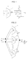
- Fig. 1 shows an illustrative diagram of a single-hysteresis voltage controlled current source element, therein Fig. 1 (a) shows a circuits symbol of a fundamental single-hysteresis element for combining a multi-hysteresis characteristic, and Fig. 1(b) shows its input and output characteristics.
- This single-hysteresis element 1 is a voltage controlled current source (VCCS) circuit of which an output current i out for a differential-input voltage v id presents the hysteresis characteristic as shown in Fig. 1 (b) .
- VCCS voltage controlled current source
- I U the output saturation current defined as an output when the differential-input voltage v id is lower than a threshold voltage E R of the hysteresis
- I D the output saturation current when the differential-input voltage v id is higher than a threshold voltage E L
- E L ⁇ E R .
- Fig. 2 shows a configuration of a multi-hysteresis voltage controlled current source system illustrating an embodiment of the present invention.
- N single-hysteresis VCCS circuits 2 1 to 2 N (N is an arbitrary positive integer) can be connected easily in parallel as shown in Fin. 2.
- an overall output current i mh can be represented by the following equation (2).
- the threshold voltages of the k-th single-hysteresis characteristics H k are denoted as E R k and E L k (E R k > E L k ).
- the saturation output current value defined by V id ⁇ E R k is denoted as I U k
- the saturation output current value defined by v id ⁇ E L k is denoted as I D k
- a binary variable b k is introduced, which is "1" if the output of the k-th single-hysteresis VCCS circuit is the saturation, output current value I U k , or otherwise "0".
- n and p are indexes, and 1 ⁇ n ⁇ N and 1 ⁇ p ⁇ H.
- the output state of the single-hysteresis characteristic contained in the multi-hysteresis characteristic is represented by the integer m described as:
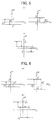
- Figs. 4-6 show first to third examples of the multi-hysteresis characteristics obtained by combining two single-hysteresis VCCS circuits.
- the relationship between the constituent two single-hysteresis VCCS circuits can be generally classified into three types: (i) one with a nested structure of the hysteresis intervals (E L 2 ⁇ E L 1 ⁇ E R 1 ⁇ E R 2 , Fig. 4 ); (ii) one with a non-overlapped structure of the hysteresis intervals (E L 1 ⁇ E R 1 ⁇ E L 2 ⁇ E R 2 , Fig. 5 ); and (iii) one with a partial-overlapped structure of the hysteresis; intervals (E L 1 ⁇ (E L 2 ⁇ (E R 1 ⁇ E R 2 , Fig. 6 )
- the total number of switching points SW of an output current value in the combined multi-hysteresis characteristics is, if all the thresholds voltages have different, values, given by:
- N is an arbitrary positive integer
- the single-hysteresis VCCS circuits constituting the multi-hysteresis VCCS system can be, as shown in Fig. 7 , made to have the characteristic that is inverse of Fig. 1(b) , i.e. I U k ⁇ I D k .
- Figs. 8-10 show first to third examples of the multi-hysteresis characteristic obtained by combining two single-hysteresis VCCS circuits having the inverse characteristic as mentioned above and the normal characteristic, respectively.
- the relationship between the respective single-hysteresis VCCS circuits constituting the multi-hysteresis VCCS system can be generally classified into three types: (i) one with a nested structure of the hysteresis intervals (E L 2 ⁇ E L 1 ⁇ E R 1 ⁇ E R 2 , Fig. 8 ); (ii) one with a non-overlapped structure of the hysteresis intervals (E L 1 ⁇ E R 1 ⁇ E L 2 ⁇ E R 2 , Fig.
- Fig. 11-15 show first to fifth examples where two single-hysteresis VCCS circuits having the hysteresis characteristics in the nested structure as shown in Fig. 4 are connected with each other, that are also connected with another single-hysteresis VCCS circuit.
- Fig. 11 shows the case where the hysteresis characteristics of three single-hysteresis VCCS circuits have the nested stricture (E L 3 ⁇ E L 2 ⁇ E L 1 ⁇ E R 1 ⁇ E R 2 ⁇ E R 3 ); Fig.
- VCCS circuit (E L 2 ⁇ E L 3 ⁇ E L 1 ⁇ E R 1 ⁇ E R 2 ⁇ E R 3 ); Fig.
- FIG. 13 shows the case where the left threshold of the hysteresis characteristic of the third single-hysteresis VCCS circuit is present inside of the threshold of the hysteresis characteristic of the first single-hysteresis VCCS circuit (E L 2 ⁇ E L 1 ⁇ E L 3 ⁇ E R 1 ⁇ E R 2 ⁇ E R 3 ); Fig.
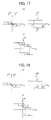
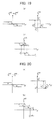
- Figs. 16-20 show sixth to tenth examples where two single-hysteresis VCCS circuits having the hysteresis intervals of the hysteresis characteristics in the non-overlapped structure as shown in Fig. 5 are connected with each other, that are also connected with another single-hysteresis VCCS circuit.
- Fig. 16 shows the case where both the left and right thresholds of the third single-hysteresis VCCS circuit are present outside of the thresholds of the hysteresis characteristics of the other two single-hysteresis VCCS circuits, respectively (E L 3 ⁇ E L 1 ⁇ E R 1 ⁇ E L 2 ⁇ E R 2 ⁇ E R 3 ); Fig.
- Figs. 5(b) and 20(b) are equivalent to the multi-hysteresis characteristics used in the above-mentioned Non-Patent Documents 12, 13, and 14, that can also be realized more easily by means of the multi-hysteresis VCCS circuit of the present invention,
- Figs. 21-25 show eleventh to fifteenth examples of the multi-hysteresis characteristic obtained by connecting two single-hysteresis VCCS circuits having the hysteresis intervals in the partial-overlapped structure as shown, in Fig. 6 , that are also connected, with another single-hysteresis VCCS circuit.
- Fig. 21-25 show eleventh to fifteenth examples of the multi-hysteresis characteristic obtained by connecting two single-hysteresis VCCS circuits having the hysteresis intervals in the partial-overlapped structure as shown, in Fig. 6 , that are also connected, with another single-hysteresis VCCS circuit.
- FIG. 22 shows the case where the left threshold of the hysteresis characteristic of the third single-hysteresis VCCS circuit is present between the left thresholds of the hysteresis characteristic of the first and second single-hysteresis VCCS circuits (E L 1 ⁇ E L 3 ⁇ E L 2 ⁇ E R 1 ⁇ E R 2 ⁇ E R 3 ); Fig.
- FIG. 23 shows the case where the left threshold of the hysteresis characteristic of the third single-hysteresis VCCS circuit is present within the overlapped hysteresis intervals of the hysteresis characteristics of the other two single-hysteresis VCCS circuits (E L 1 ⁇ E L 2 ⁇ E L 3 ⁇ E R 1 ⁇ E R 2 ⁇ E R 3 ); Fig.
- FIG. 24 shows the case where the left threshold of the hysteresis characteristic of the third single-hysteresis VCCS circuits is present within the overlapped hysteresis intervals of the hysteresis characteristics of the other two single-hysteresis VCCS circuits, while the right threshold of the hysteresis characteristic of the third single-hysteresis VCCS circuit is present between the right thresholds of the hysteresis characteristic of the first and second single-hysteresis VCCS circuits (E L 1 ⁇ E L 2 ⁇ E L 3 ⁇ E R 1 ⁇ E R 3 ⁇ E R 2 ); and Fig.
- Figs, 26-30 show first to fifth examples of the multi-hysteresis characteristic where two circuits having the hysteresis interval in the nested structure as shown in Fig. 8 are also connected with another single-hysteresis VCCS circuits.
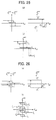
- Fig. 26 shows the case where the hysteresis characteristics of three single-hysteresis VCCS circuit have the nested structure (E L 3 ⁇ E L 2 ⁇ E L 1 ⁇ E R 1 ⁇ E R 2 ⁇ E R 3 ); Fig.
- FIG. 27 shows the case where the left thresholds of the hysteresis characteristics of the third single-hysteresis VCCS circuit is present between the left thresholds of the hysteresis characteristics of the first and second single-hysteresis VCCS circuits (E L 2 ⁇ E L 3 ⁇ E L 1 ⁇ E R 1 ⁇ E R 2 ⁇ E R 3 ); Fig.
- FIG. 29 shows the case where the left threshold of the hysteresis characteristic of the third single-hysteresis VCCS circuits is present inside of the left thresholds of the hysteresis characteristics of the other two single-hysteresis VCCS circuits, while the right threshold of the hysteresis characteristic of the third single-hysteresis VCCS circuit is present between the right thresholds of the hysteresis characteristics of the first and second single-hysteresis VCCS circuits (E L 2 ⁇ E L 1 ⁇ E L 3 ⁇ E R 1 ⁇ E R 3 ⁇ E R 2 ); and Fig.
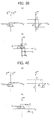
- Figs. 31-35 show sixth to tenth examples of the multi-hysteresis characteristic where two single-hysteresis VCCS circuits having the single-hysteresis characteristics inverse with each other with the non-overlapped hysteresis interval as shown in Fig. 9 are connected in parallel, that are also connected with another single-hysteresis VCCS circuits.
- Fig. 31-35 show sixth to tenth examples of the multi-hysteresis characteristic where two single-hysteresis VCCS circuits having the single-hysteresis characteristics inverse with each other with the non-overlapped hysteresis interval as shown in Fig. 9 are connected in parallel, that are also connected with another single-hysteresis VCCS circuits.
- Fig, 34 shows the case where the left threshold of the hysteresis characteristic of the third single-hysteresis VCCS circuit is present within the hysteresis interval of the hysteresis characteristics of the second single-hysteresis VCCS circuit (E L 1 ⁇ E R 1 ⁇ E L 2 ⁇ E L 3 ⁇ E R 2 ⁇ E R 3 );
- Fig, 34 shows the case where the left threshold of the hysteresis characteristics of the third single-hysteresis VCCS circuit is present within the hysteresis interval of the hysteresis characteristics of the first single-hysteresis VCCS circuit, while the right threshold of the hysteresis characteristic of the third single-hysteresis VCCS circuit is present within the hysteresis interval of the hysteresis characteristic of the second single-hysteresis VCCS circuit (E L 1 ⁇ E L
- Figs. 36-40 show eleventh to fifteenth examples of the characteristic where two single-hysteresis VCCS circuits having the hysteresis characteristics in the partial-.overlapped stricture was shown in Fig. 10 are connected, that are also connected with another single-hysteresis VCCS circuit.
- Fig. 36-40 show eleventh to fifteenth examples of the characteristic where two single-hysteresis VCCS circuits having the hysteresis characteristics in the partial-.overlapped stricture was shown in Fig. 10 are connected, that are also connected with another single-hysteresis VCCS circuit.
- FIG. 37 shows the case where the left threshold of the hysteresis characteristic of the third single-hysteresis VCCS circuit is present between the left thresholds of the hysteresis characteristics of the first and second single-hysteresis VCCS circuits E L 1 ⁇ E L 3 ⁇ E L 2 ⁇ E R 1 ⁇ E R 2 ⁇ E R 3 ); Fig.
- Fig, 39 shows the case where the left threshold of the hysteresis characteristic of the third single-hysteresis VCCS circuit is present within the overlapped hysteresis intervals of the hysteresis characteristics of the other two single-hysteresis VCCS circuits, while the right threshold of the hysteresis characteristic of the third single-hysteresis VCCS circuit is present between the right thresholds of the hysteresis characteristics of the first and second single-hysteresis VCCS circuits (E L 1 ⁇
- the multi-hysteresis VCCS system of the present invention is constituted by a plurality of single-hysteresis VCCS circuits connected in parallel.
- Fig. 41 shows an implementation of the single-hysteresis circuit with a fully-differential configuration serving as the fundamental components (see Non-Patent Documents 15, 16, and 17 above proposed by the present inventors).
- This circuit is mainly constituted by an operational transconductance amplifier (OTA) and a latch circuit.
- OTA operational transconductance amplifier
- M 19 The output voltage of the OTA (M 7 to M 19 ) serve as the input voltage of the latch circuits (M 1 to M 6 ).
- the latch circuit is constituted by a differential pair (M1, M 2 ), current sources (M 5 , M 6 ), and a pair of crosscoupled MOSFETs (M 3 , M 4 ).
- M1, M 2 the current that flows to the MOSFET M 2 increases, so that the drain, voltage of the MOSFET M 2 , i.e. the source voltage of the MOSFET M 4 , drops.
- the drain voltage of the MOSFET M 4 i.e. the gate voltage of the MOSFET M 3
- the current flowing to the MOSFET M 3 decreases and the drain voltage of the MOSFET M 3 , i.e.
- the gate voltage of the MOSFET M 4 rises. Thereby, the drain current of the MOSFET M 4 , increases further and the drain voltage of the MOSFET M 4 , i.e. the gate voltage of the MOSFET M 3 , drops further. This generates the positive feedback so that the steep falling characteristic of the drain voltage of the MOSFET M 4 is obtained. Then, while the current that flows to the MOSFET M 2 tries to decrease as the gate voltage of the MOSFET M 2 drops, the gate of the MOSFET M 4 is kept at a high potential because of the positive feedback and thus the current to the MOSFET M 2 cannot decreases rabidly. As a result, the drain voltage of the MOSFET M 2 , i.e.
- the source voltage of the MOSFET M 4 rises and the gate-source voltage of the MOSFET M 4 decreases.
- the gate-source voltage of the MOSFET M 4 decreases to a curtain value
- the drain voltage of the MOSFET M 4 rises and the MOSFET M 3 is suddenly turned ON while the MOSFET M 4 , is turned OFF because of the positive feedback. In this manner, the steep rising characteristic of the drain voltage of the MOSFET M 4 can be obtained.
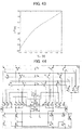
- Fig. 42 shows V id -i 0 + characteristics obtained from the SPICE simulation using the fully-differential single-hysteresis VCCS circuit shown in Fig. 41 where the external control voltages V he are set to 1.2 V, 1.24 V, and 1.29 V, respectively.
- Table 1 shows the sizes of each transistor in Fig. 41 used in this simulation.
- the multi-hysteresis system can be realized buy connecting a plurality of the fully-differential single-hysteresis VCCS circuits described above in parallel.
- Fig. 44 shows an example of the multi-hysteresis system incorporating three fully-differential single-hysteresis VCCS circuits.
- triangular symbol (h 1 , h 2 , h 3 ) represent core circuit portions forked of transistors, MOSFETs M 1 to M 9 , in Fig. 41 .
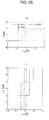
- Fig. 45 shows result of the SPICE simulation for the multi-hysteresis VCCS system shown in Fig. 44
- Table 2 shows the sizes of the transistors used in this simulation.
- FIG. 45(a) shows superimposed input and output characteristics of three single-hysteresis VCCS circuits having different threshold voltages contained in the circuits in Fig. 44 .
- Fig. 45 (b) shows the multi-hysteresis characteristic which was realized by combining these circuits.
- Figs. 46(a), (b), and (c) show the characteristics of the fully-differential multi-hysteresis VCCS system obtained from the SPICE stimulations where the relationship among the thresholds were similar to those of the characteristics shown in Figs. 12(b) , 13(b), and 14(b) , respectively.
- Table 3 shows the external control voltages used in these simulations.
- the characteristics were measured by keeping V in - terminals of the single-hysteresis VCCS circuits (h 1 to h 3 ) at the voltages V w1 to V w3 , respectively, and changing a common voltage.
- the multi-hysteresis voltage controlled current sources system providing the multi-hysteresis VCCS characteristic can be realized by connecting the single-hysteresis VCCS circuits in parallel.
- the circuit examples for realizing the multi-hysteresis VCCS characteristics and the SPICE simulation result of the circuits there has been provided the circuit examples for realizing the multi-hysteresis VCCS characteristics and the SPICE simulation result of the circuits.
- the diverse multi-hysteresis VCCS characteristics can be realized easily by the multi-hysteresis voltage controlled current source system of the present invention.
- the characteristics of the single-hysteresis VCCS circuits constituting the multi-hysteresis voltage controlled current source circuits can be set asp independently from each other, the shape of the combined multi-hysteresis characteristic can be controlled easily using the external voltages which control the characteristics of the respective single-hysteresis VCCS circuits, As such, the number of stages or the shapes of the hysteresis characteristics, as well as the multi-hysteresis characteristics including the thresholds and the saturation current values, can be controlled even during the operation of the circuit, allowing more diverse operations.
- the multi-hysteresis voltage controlled current source system of the present invention is applicable to the realization of multi-hysteresis chaotic oscillators presenting very complex attractors or the constitution of large-scaled and complex hybrid dynamical systems, as well as the implementation of multivalued logic function circuits or multivalued memory circuits and multi-hysteresis neutral networks utilizing multivalued statuses.
Landscapes
- Manipulation Of Pulses (AREA)
- Amplifiers (AREA)
Abstract
Description
- The present invention relates to a multi-hysteresis voltage controlled current source (VCCS) system.
- In resent years, active researchers have been conducted on the "hybrid dynamical system" that contains the continuous variable and the discrete variable ire the system. Although the exiting computer systems are constituted as a discrete system based on the binary-logic variables, the pretence or the hybrid dynamical systems equivalent to the Tuning machines has been proved mathematically (see Non-Patent
Document 1 blow) Thugs, there is a possibility that the computing systems different from the existing digital computers can be constituted using the hybrid dynamical systems. Moreover, when the hybrid dynamical system presents very complex phenomena such has chaos, the dynamic and complex information processing methods are also conceivably by representing the attractors of the continuos variable with discrete values. - On the other hard, the chaos, generating circuits musing hysteresis Elements have been proposed (see Non-Patent Documents 2-11 below). These circuits use the piecewise lineal single-hysteresis elements as non-linear elements, and a variety of interesting chaotic attractors have been reported. Moreover, in order to make the chaotic attractors more diverse, the method has been proposed wherein the single-hysteresis elements are replaced by multi-hysteresis elements that can obtain multivalued outputs (see Non-Patent Document 12-14 below). In this method, grid-scroll chaotic attractors or the like can be observed. The shapes of such complex chaotic attractors defend on the multi-hysteresis characteristics two be used.
-
- Non-Patent Document 1: Michael S. Branicky, "Universal computation and other capabilities of hybrid and continuous dynamical system", Theoretical Computer Science, vol. 138, pp. 67-100, 1995
- Non-Patent Documents 2: R. W. Newcomb and S. Sathyan, "An RC op amp chaos generator", IEEE Trans. on Circuits and Systems, Part I, Fundam. Theory Appl., vol. 30, no. 1, pp. 54-56, 1983
- Non-Patent Document 3: R. W. Newcomb and N. El-Leithy, to binary hysteresis chaos generator", in Proc. of 1984 IEEE Int'l Symp. on Circuits and Systems, pp. 856-859, 1984
- Non-Patent. Document 4: Toshimichi Saito, "On a hysteresis chaos generator", in Proc. of 1985 IEEE Int'l Symp. on Circuits and Systems, pp. 847-849, 1985
- Non-Patent Documents 5: Takashi Suzuki and Toshimichi Saito, "On fundamental bifurcations from a hysteresis hyperchaos generator", IEEE Trans. on Circuits and Systems, Part I, Fundam. Theory Appl., vol. 41, no. 12, pp. 876-884, 1994
- Non-Patent Document 6: Toshimichi Saito and Shinji Nakagawa, "chaos from a hysteresis and switched circuit", Phil. Trans. R. Soc. Lend. A, vol. 353, no. 1701, pp. 47-57, 1995
- Non-Patent Document 7 : Toshimichi Saito and Kunihiko Mitsubori, "Control of chaos from a piecewise liner hysteresis circuits", IEEE Trans. on Circuits and Systems, Part I, Fundam. Theory Appl., vol. 42, no. 3, pp. 168-172, 1995
- Non-Patent Document 8: J. E. Varrientos and E. Sanchez-Sinencio, "A 4-D chaotic oscillator based on a differential hysteresis comparator", IEEE Trans. on Circuits and Systems, Part I, Fundam. Theory Appl. vol. 45, no. 1, pp. 3-10, 1998
- Non-Patent Document 9: A. S. Elwakil and M. P. Kennedy, "Chaotic Oscillators derived from Saito's double-screw hysteresis oscillator", IEICE Trans. Fundamental, vol. E82-A, no. 9, pp. 1769-1775, 1999
- Non-Patent Document 10: Masaki Kataoka and Toshimichi Saito, "A 2-sport VCCS chaotic oscillator and quad screw attractor", IEEE trans. on Circuits and System, Part I, Fundam. Theory Appl., vol. 48, no. 2, pp. 221-225, 2001 Non-Patent Document 11: F. Bizzarri, D. Stellardo, and M. Storace, "Bifurcation analysis and its experimental validation for a hysteresis circuit oscillator", IEEE Trans. on Circuits and System, Part I, Regular paupers, vol. 53, no. 7, pp. 517-521, 2006
- Non-Patent Document 12: Fengling Han, Xinghuo Yu, Yuye Wang, Yong Feng, and Guanrong Chen, "n-scroll chaotic oscillators by second-order systems and double-hysteresis blocks", Electronics Letters, vol. 39, no. 23, pp. 1636-1637, 2003
- Non-Patent Document 13: Fengling Ham, Xinghuo Yu, and Jiankun Hu, "A new way of generating grid-scroll chaos and its application to biometric authentication", in Proc. of IEEE 2005 Industrial Electronics Society, 31st Annul Conference, pp. 61-66, 2005
- Non-patent Document 14: Fengling Han, Xinghao Yu, Yong Feng, and Tiankun Hu, "On multiscroll chaotic attractors in hysteresis-based piecewise-linear systems", IEEE Trans. on Circuits and Systems, Part II, Express Briefs, vol. 54, no. 11, pp. 1004-1008, 2007
- Non-Patent Document 15: Takuya Hamada, Yoshihiko Horio, and Kazuyuki Aihara, "An IC implementation of a hysteresis two-port VCCS chaotic oscillator", in Proc. of European Conf. on Circuits Theory and Design, pp. 926-929, 2007
- Non-Patent Document 16: Takuya Hamada, Yoshihiko Horio, and Kazuyuki Aihara, "Experimental observations from an integrated hysteresis two-port VCCS chaotic oscillator", in Proc. IEEE Int'l Work-shop on Nonlinear Dynamics of Electronic Systems, pp. 237-240, 2007
- Non-Patent Document 17: Takuya Hamada, Yoshihiko Horio, and Kazuyuki Aihara, "A Fully-Differential Hysteresis Two-Port VCCS Chaotic Oscillator", IEICE Technical Report, NLP2007-180, pp. 79-84, 2008
- The systems having a variety of multi-hysteresis characteristics are indispensable to create various information processing features. However, the multi-hysteresis system proposed in the above-mentioned Non-Patent Documents 12-14 only presents the characteristic where the single-hysteresis characteristic are combined in series. In addition, such a multi-hysteresis characteristic is constituted by connecting a plurality of voltage controlled voltage source circuits (VCVS Circuits) having the single-hysteresis characteristics. Since inputs and outputs of this type of VCVS circuits are both voltages, connecting a plurality of circuits requires an adder, resulting in the increase in scale of the circuits.
- In view of the circumstances described above, the present invention is directed to provide a multi-hysteresis voltage controlled current sources system having a variety of multi-hysteresis characteristics.
- In order to achieve the object described above, the present invention provides the following:
- [1] A multi-hysteresis voltage controlled current source systems constituted by connecting single-hysteresis voltage controlled current source circuits as fundamental components on parallel, and applying a differential input voltages to the single-hysteresis voltage controlled current source circuits, so that a plurality of discrete values of current can be output based on the single-hysteresis voltage controlled current source circuits.
- [2] The multi-hysteresis voltage controlled current source system according to [1] above, wherein characteristics of the single-hysteresis voltage controlled current source circuits are enabled to be set independently from each other, so that changing the characteristics allows a variety of -hysteresis VCCS characteristics to be obtained.
- [3] The multi-hysteresis voltage controlled current source systems according to [1] or [2] above, wherein N single-hysteresis voltage controlled current sources circuits (N is an arbitrary positive integer) are connected tin parallel.
- [4] The multi-hysteresis voltage controlled current source system according to [1] or [2] above, wherein the single-hysteresis voltage controlled current sources circuits connected in parallel include only a combination of circuits having a normal hysteresis characteristic.
- [5] The multi-hysteresis voltages controlled current source system according to [1] or [2] above, wherein the single-hysteresis voltage controlled current source circuits connected in parallel include only a combination of circuits having an inverse hysteresis characteristic.
- [6] The multi-hysteresis voltage controlled current source system according to [1] or [2] above, wherein the single-hysteresis voltage controlled current source circuits connected in parallel include a combination of a circuit having the normal hysteresis characteristic and a circuit having the inverse hysteresis characteristic.
- [7] The multi-hysteresis voltage controlled current source system according to [6] above, wherein the single-hysteresis voltage controlled current source circuits connected in parallel include a combination of two circuits each having the normal hysteresis characteristic and the inverse hysteresis characteristic.
- [8] The multi-hysteresis voltage controlled current source system according to [4], [5], or [6] above, wherein three single-hysteresis voltage controlled current source circuits are connected in parallel.
- [9] The multi-hysteresis voltage controlled current source system according to [1] or [2] above, wherein the single-hysteresis voltage controlled current source circuits connected in parallel include an operational transconductance amplifier (OTA) and a latch circuits.
- [10] The multi-hysteresis voltage controlled current source system according to [9] above, wherein a range of threshold voltages is changed by controlling external control voltage (Vhe) of the latch circuit.
- [11] The multi-hysteresis voltage controlled current source system according to [1] or [2] above, wherein the single-hysteresis voltage controlled current source circuit connected in parallel incorporate three fully-differential single-hysteresis voltage controlled current source circuits.
- A multi-hysteresis voltage controlled current source system of the present invention enables a multi-hysteresis VCCS circuit to be constituted easily by combining a plurality of single-hysteresis VCCS circuits in parallel of which the input is voltage and the output is current.
- Moreover, the single-hysteresis VCCS circuits as a component of the multi-hysteresis VCCS circuit can be set up its characteristics independently from each other, so that changing the characteristics allows a variety of multi-hysteresis VCCS characteristics to be realized easily.
-
-
Fig. 1 shows an illustrative diagram of a single-hysteresis voltage controlled current source element; -
Fig. 2 shows a configuration of a multi-hysteresis voltage controlled current source system illustrating an embodiment of the present invention; -
Fig. 3 shows the circuit symbol of a multi-hysteresis voltage controlled current element illustrating an embodiment of the present invention; -
Fig. 4 shows a first example of a multi-hysteresis characteristic constituted by connecting two single-hysteresis VCCS circuits in parallel; -
Fig. 5 shows a second example of the multi-hysteresis characteristic constituted by connecting two single-hysteresis VCCS circuits in parallel; -
Fig. 6 shows a third example of the multi-hysteresis characteristic constituted by connecting two single-hysteresis VCCS circuits in parallel; -
Fig. 7 shows a characteristic of the inverse single-hysteresis VCCS; -
Fig. 8 shows a first example of the multi-hysteresis characteristics constituted by connecting the single-hysteresis VCCS circuits in parallel, of which one having a normal hysteresis; and one having an inverse hysteresis; - Pig. 9 shows a second example of the multi-hysteresis characteristic constituted by connecting the single-hysteresis VCCS circuits in parallel, of which one having the normal hysteresis and one having the inverse hysteresis;
-
Fig. 10 shows a third example of the multi-hysteresis characteristics constituted by connecting the single-hysteresis VCCS circuits in parallel, of which one having the normal hysteresis and one having the inverse hysteresis; -
Fig 11 shows a first example of the multi-hysteresis characteristic constituted by connecting three single-hysteresis VCCS circuits in parallel; -
Fig. 12 shows a second example of the multi-hysteresis characteristic constituted by connecting three single-hysteresis VCCS circuits in parallel; -
Fig. 13 shows a third example of the multi-hysteresis characteristic constituted by connecting three single-hysteresis VCCS circuits in parallel; -
Fig. 14 shows a fourth example of the multi-hysteresis characteristic constituted by connecting three single-hysteresis VCCS circuits in parallel; -
Fig. 15 shows a fifth example of the multi-hysteresis characteristic constituted by connecting three single-hysteresis VCCS circuits in parallel; -
Fig. 16 shows a sixth example of the multi-hysteresis characteristic constituted by connecting three single-hysteresis VCCS circuits in parallel; -
Fig. 17 shows a seventh example of the multi-hysteresis characteristics constituted by connecting three single-hysteresis VCCS circuits in parallel; -
Fig. 18 shows an eighth example of the multi-hysteresis characteristics constituted by connecting three single-hysteresis VCCS circuits in parallel; -
Fig. 19 shows a ninth example of the multi-hystereses characteristic constituted by connecting three single-hysteresis VCCS circuits in parallel; -
Fig. 20 shows a tenth example of the multi-hysteresis characteristic constituted by connecting three single-hysteresis VCCS circuits in parallel; -
Fig. 21 shows an eleventh example of the multi-hysteresis characteristic constituted by connecting three single-hysteresis VCCS circuits in parallel; -
Fig. 22 shows a twelfth example of the multi-hysteresis characteristic constituted by connecting three single-hysteresis VCCS circuits in parallel; -
Fig. 23 shows a thirteenth example of the multi-hysteresis characteristic constituted by connecting three single-hysteresis VCCS circuits in parallel; -
Fig. 24 shows a fourteenth example of the multi-hysteresis characteristics constituted by connecting three single-hysteresis VCCS circuits in parallel; -
Fig. 25 shows a fifteenth example of the multi-hysteresis characteristics constituted by connecting three single-hysteresis VCCS circuit in parallel; -
Fig. 26 shows a first example or the multi-hysteresis characteristic constituted by connecting three single-hysteresis VCCS circuits in parallel, that include the inverse hysteresis; -
Fig. 27 shows a second example or the multi-hysteresis characteristic constituted by connecting three single-hysteresis VCCS circuits in parallel, that include the inverse hysteresis; -
Fig. 28 shows a third example of the multi-hysteresis characteristic constituted by connecting three single-hysteresis VCCS circuits in parallel, that include the inverse hysteresis; -
Fig. 29 shows a fourth example of the multi-hysteresis characteristic constituted by connecting three single-hysteresis VCCS circuits in parallel, that include the inverse hysteresis; -
Fig. 30 shows a fifth example of the multi-hysteresis characteristic constituted by connecting three single-hysteresis VCCS circuits in parallel, that include the inverse hysteresis; -
Fig. 31 shows a sixth example of the multi-hysteresis characteristic constituted by connecting three single-hysteresis VCCS circuits if parallel, that include the inverse hysteresis; -
Fig. 32 shows a seventh example of the multi-hysteresis characteristic constitutes by connecting three single-hysteresis VCCS circuits in parallel, that include the inverse hysteresis; -
Fig. 33 shows an eighth example of the multi-hysteresis characteristic constituted by connecting three single-hysteresis VCCS circuits in parallel, that include the inverse hysteresis; -
Fig. 34 shows a ninth example of the multi-hysteresis characteristic constituted by connecting three single-hysteresis VCCS circuits in parallel, that include the inverse hysteresis; -
Fig. 35 shows a tenth example of the multi-hysteresis characteristic constituted by connecting three single-hysteresis VCCS circuits in parallel, that include the inverse hysteresis; -
Fig. 36 shows an eleventh example of the multi-hysteresis characteristic constituted by connecting three single-hysteresis VCCS circuit in parallel, that include the inverse hysteresis; -
Fig. 37 shows a twelfth example of the multi-hysteresis characteristic constituted by connecting three single-hysteresis VCCS circuit in parallel, that include the inverse hysteresis; -
Fig. 38 shows a thirteenth example of the multi-hysteresis characteristic constituted by connecting three single-hysteresis VCCS circuits in parallel, that include the inverse hysteresis; -
Fig. 39 shows a fourteenth example of the multi-hysteresis characteristic constituted by connecting three single-hysteresis VCCS circuits in parallel, that include the inverse hysteresis; -
Fig. 40 shows a fifteenth example of the multi-hysteresis characteristic constituted by connecting three single-hysteresis VCCS circuits in parallel, that include the inverse hysteresis; -
Fig. 41 shows a circuits diagram of a fully-differential single-hysteresis VCCS; -
Fig. 42 shows a characteristic of the fully-differential single-hysteresis VCCS circuit when its external control voltage Vhe is changed; -
Fig. 43 shows a change in threshold voltage ER for the external control voltage Vhe; -
Fig. 44 shows a configuration of a fully-differential multi-hysteresis VCCS system (N = 3); -
Fig. 45 shows a Vid-i0 + characteristic of the fully-differential multi-hysteresis VCCS system; and -
Fig. 46 shows a characteristic of the fully-differential multi-hysteresis VCCS system obtained from the SPICE simulation. - A multi-hysteresis voltage controlled current source system according to the present invention is constituted by connecting single-hysteresis voltage controlled current source circuits as fundamental components in parallel, so that a plurality of discrete values of current can be output based on the single-hysteresis voltage controlled current source circuits.
- Hereinafter, embodiments of the present invention will be described in detail.
- A method of realizing a multi-hysteresis VCCS characteristic of the present invention will be described.
-
Fig. 1 shows an illustrative diagram of a single-hysteresis voltage controlled current source element, thereinFig. 1 (a) shows a circuits symbol of a fundamental single-hysteresis element for combining a multi-hysteresis characteristic, andFig. 1(b) shows its input and output characteristics. - This single-
hysteresis element 1 is a voltage controlled current source (VCCS) circuit of which an output current iout for a differential-input voltage vid presents the hysteresis characteristic as shown inFig. 1 (b) . Among two saturation currents shown inFig. 1(b) , the output saturation current defined as an output when the differential-input voltage vid is lower than a threshold voltage ER of the hysteresis is denoted as IU, and the output saturation current when the differential-input voltage vid is higher than a threshold voltage EL is denoted as ID Here, note that EL < ER. When the differential-input voltage vid reaches ER while the output current iout is IU, the output current iout is twitched to ID. Similarly, when the differential-input voltage vid reaches EL while the output current iout is ID, the output current iout is switched to IU. therefore, a vid-iout characteristic of this circuit is described by the following equation (1). -

-
Fig. 2 shows a configuration of a multi-hysteresis voltage controlled current source system illustrating an embodiment of the present invention. - Since the above-described single-hysteresis VCCS circuit is a current output type, N single-
hysteresis VCCS circuits 21 to 2N (N is an arbitrary positive integer) can be connected easily in parallel as shown in Fin. 2. In this regard, an overall output current imh can be represented by the following equation (2). -

Fig. 2 , if each single-hysteresis characteristic Hk(vid) has a different, threshold values, the overall output current imh has the multi-output hysteresis characteristic of multivalued outputs, i.e. the multi-hysteresis characteristic. Such an element of which the overall output current imh for the differential-input voltage vid has the multi-hysteresis characteristic is represented by the symbol shown inFig. 3 hereinbelow. - Here, the threshold voltages of the k-th single-hysteresis characteristics Hk(Vid) are denoted as ER k and EL k (ER k > EL k). In addition, the saturation output current value defined by Vid ≤ ER k is denoted as IU k, and the saturation output current value defined by vid ≥ EL k is denoted as ID k Moreover, as described in the following equation (3), a binary variable bk is introduced, which is "1" if the output of the k-th single-hysteresis VCCS circuit is the saturation, output current value IU k, or otherwise "0".
-

-

bk represents the inversion of bk. Moreover,

- On the other hand, the output state of the single-hysteresis characteristic contained in the multi-hysteresis characteristic is represented by the integer m described as:
-

- As the most simplified configuration examples of the multi-hysteresis VCCS system of the present invention,
Figs. 4-6 show first to third examples of the multi-hysteresis characteristics obtained by combining two single-hysteresis VCCS circuits. - As shown in these figures, the relationship between the constituent two single-hysteresis VCCS circuits can be generally classified into three types: (i) one with a nested structure of the hysteresis intervals (EL 2 ≤ EL 1 < ER 1 ≤ ER 2,
Fig. 4 ); (ii) one with a non-overlapped structure of the hysteresis intervals (EL 1 < ER 1 ≤ EL 2 < ER 2,Fig. 5 ); and (iii) one with a partial-overlapped structure of the hysteresis; intervals (EL 1 ≤ (EL 2 < (ER 1 ≤ ER 2,Fig. 6 ) - In general, when the hysteresis intervals of N single-hysteresis VCCS circuits (N is an arbitrary positive integer) constitutes the nested structure with each other [(i)], the total number of switching points SW of an output current value in the combined multi-hysteresis characteristics is, if all the thresholds voltages have different, values, given by:
-

Fig. 4(b) , there are six output switching points. - On the other hand, when the hysteresis intervals of the constituent single-hysteresis characteristics do not overlap at all [(ii)] or only some of them overlap [(iii)], the total number of the switching points SW of the output current value in the multi-hysteresis characteristic combined by N single-hysteresis VCCS circuits (N is an arbitrary positive integer) is, if all the threshold voltage have different values, given by: SM = 2N ...(7) For example, in the cases of
Figs. 5(b) and 6(b) , there are for output switching points, respectively. - Here, the single-hysteresis VCCS circuits constituting the multi-hysteresis VCCS system can be, as shown in
Fig. 7 , made to have the characteristic that is inverse ofFig. 1(b) , i.e. IU k < ID k.Figs. 8-10 show first to third examples of the multi-hysteresis characteristic obtained by combining two single-hysteresis VCCS circuits having the inverse characteristic as mentioned above and the normal characteristic, respectively. - Again in this case, the relationship between the respective single-hysteresis VCCS circuits constituting the multi-hysteresis VCCS system can be generally classified into three types: (i) one with a nested structure of the hysteresis intervals (EL 2 ≤ EL 1 < ER 1 ≤ ER 2,
Fig. 8 ); (ii) one with a non-overlapped structure of the hysteresis intervals (EL 1 < ER 1 ≤ EL 2 < ER 2,Fig. 9 ); and (iii) one with a partial-overlapped structure of the hysteresis intervals (EL 1 ≤ EL 2 < ER 1 ≤ ER 2,Fig. 10 ). When the hysteresis intervals constitute the nested structure with each other [(i)], the total number of the switching points SW of the output saturation current of the multi-hysteresis characteristic is given by the equation (6) above, and in other cases [(ii), (iii)], it is given by the equation (7) above. - Next, the examples of the multi-hysteresis characteristics in the case where three single-hysteresis VCCS circuits are connected in parallel will be described.
- First,
Fig. 11-15 show first to fifth examples where two single-hysteresis VCCS circuits having the hysteresis characteristics in the nested structure as shown inFig. 4 are connected with each other, that are also connected with another single-hysteresis VCCS circuit.Fig. 11 shows the case where the hysteresis characteristics of three single-hysteresis VCCS circuits have the nested stricture (EL 3 ≤ EL 2 ≤ EL 1 < ER 1 ≤ ER 2 ≤ ER 3);Fig. 12 shows the case where the left threshold of the hysteresis characteristic of the third single-hysteresis VCCS circuit is present between the left thresholds of the hysteresis characteristic of the first and second single-hysteresis. VCCS circuit (EL 2 ≤ EL 3 ≤ EL 1 < ER 1 ≤ ER 2 ≤ ER 3);Fig. 13 shows the case where the left threshold of the hysteresis characteristic of the third single-hysteresis VCCS circuit is present inside of the threshold of the hysteresis characteristic of the first single-hysteresis VCCS circuit (EL 2 ≤ EL 1 ≤ EL 3 < ER 1 ≤ ER 2 ≤ ER 3);Fig. 14 shows the case where the left threshold of the hysteresis characteristic of the third single-hysteresis VCCS circuit is present inside of the threshold of the hysteresis characteristics of the second single-hysteresis VCCS circuit, while the right threshold of the hysteresis characteristic of the third single-hysteresis VCCS circuit is present between the right thresholds of the hysteresis characteristics of the first and second single-hysteresis VCCS circuits (EL 2 ≤ EL 1 ≤ EL 3 < ER 1 ≤ ER 3 ≤ ER 2); andFig. 15 shows the case where the hysteresis interval of the hysteresis characteristic of the third single-hysteresis VCCS circuit does not overlap with the hysteresis characteristic of the other single-hysteresis VCCS circuits (EL 2 ≤ EL 1 < ER 1 ≤ ER 2 ≤ EL 3 < ER 3). - Moreover,
Figs. 16-20 show sixth to tenth examples where two single-hysteresis VCCS circuits having the hysteresis intervals of the hysteresis characteristics in the non-overlapped structure as shown inFig. 5 are connected with each other, that are also connected with another single-hysteresis VCCS circuit.Fig. 16 shows the case where both the left and right thresholds of the third single-hysteresis VCCS circuit are present outside of the thresholds of the hysteresis characteristics of the other two single-hysteresis VCCS circuits, respectively (EL 3 ≤ EL 1 < ER 1 ≤ EL 2 < ER 2 ≤ ER 3);Fig. 17 shows the case where the left threshold of the hysteresis; characteristic of the third single-hysteresis VCCS circuits is present within the hysteresis interval of the hysteresis characteristic of the first single-hysteresis VCCS circuit (EL 1 ≤ EL 3 < ER 1 ≤ EL 2 < ER 2 ≤ ER 3);Fig. 18 shows the case where the left thresholds of the hysteresis characteristic of the third single-hysteresis VCCS circuit is present within the hysteresis intervals of the hysteresis characteristic of the second single-hysteresis VCCS circuit (EL 1 < ER 1 < EL 2 ≤ EL 3 < ER 2 ≤ ER 3);Fig. 19 shows the case where the left threshold of the hysteresis characteristic of the third single-hysteresis VCCS circuit is present within the hysteresis interval of the hysteresis characteristic of the first single-hysteresis VCCS circuit, while the right threshold is present within the hysteresis interval of the hysteresis characteristic of the second single-hysteresis VCCS circuit (EL 1 ≤ EL 3 < ER 1 < EL 2 ≤ ER 3 < ER 2); andFig. 20 shows the case where the hysteresis interval of the hysteresis characteristic of the third single-hysteresis VCCS circuit does not overlap with the hysteresis intervals of the hysteresis characteristics of the other two single-hysteresis VCCS circuits (EL 1 < ER 1 ≤ RL 2 < ER 2 ≤ EL 3 < ER 3). - Among those described above, the characteristics in
Figs. 5(b) and20(b) are equivalent to the multi-hysteresis characteristics used in the above-mentionedNon-Patent Documents - Furthermore,
Figs. 21-25 show eleventh to fifteenth examples of the multi-hysteresis characteristic obtained by connecting two single-hysteresis VCCS circuits having the hysteresis intervals in the partial-overlapped structure as shown, inFig. 6 , that are also connected, with another single-hysteresis VCCS circuit.Fig. 21 shows the case where both the left and right thresholds of the hysteresis characteristic of the third single-hysteresis VCCS circuit are present outside of the thresholds of the hysteresis characteristic of the other two single-hysteresis VCCS circuits, respectively (EL 3 ≤ EL 1 ≤ EL 2 < ER 1 ≤ ER 2 ≤ ER 3);Fig. 22 shows the case where the left threshold of the hysteresis characteristic of the third single-hysteresis VCCS circuit is present between the left thresholds of the hysteresis characteristic of the first and second single-hysteresis VCCS circuits (EL 1 ≤ EL 3 ≤ EL 2 < ER 1 ≤ ER 2 ≤ ER 3);Fig. 23 shows the case where the left threshold of the hysteresis characteristic of the third single-hysteresis VCCS circuit is present within the overlapped hysteresis intervals of the hysteresis characteristics of the other two single-hysteresis VCCS circuits (EL 1 ≤ EL 2 ≤ EL 3 < ER 1 ≤ ER 2 ≤ ER 3);Fig. 24 shows the case where the left threshold of the hysteresis characteristic of the third single-hysteresis VCCS circuits is present within the overlapped hysteresis intervals of the hysteresis characteristics of the other two single-hysteresis VCCS circuits, while the right threshold of the hysteresis characteristic of the third single-hysteresis VCCS circuit is present between the right thresholds of the hysteresis characteristic of the first and second single-hysteresis VCCS circuits (EL 1 ≤ EL 2 ≤ EL 3 < ER 1 ≤ ER 3 ≤ ER 2); andFig. 25 shows the case where the hysteresis interval of the hysteresis; characteristic of the third single-hysteresis VCCS circuits does not overlap with the hysteresis intervals of the hysteresis characteristics of the other two single-hysteresis VCCS circuits (EL 1 ≤ EL 2 < ER 1 ≤ ER 2 ≤ EL 3 < ER 3). - Newt, an example will be described where two single-hysteresis VCCS circuits having inverse characteristic with each other are connected, that are further connected with a third single-hysteresis VCCS circuit.
- First,
Figs, 26-30 show first to fifth examples of the multi-hysteresis characteristic where two circuits having the hysteresis interval in the nested structure as shown inFig. 8 are also connected with another single-hysteresis VCCS circuits.Fig. 26 shows the case where the hysteresis characteristics of three single-hysteresis VCCS circuit have the nested structure (EL 3 ≤ EL 2 ≤ EL 1 < ER 1 ≤ ER 2 ≤ ER 3);Fig. 27 shows the case where the left thresholds of the hysteresis characteristics of the third single-hysteresis VCCS circuit is present between the left thresholds of the hysteresis characteristics of the first and second single-hysteresis VCCS circuits (EL 2 ≤ EL 3 ≤ EL 1 < ER 1 ≤ ER 2 ≤ ER 3);Fig. 28 shows the case where the left threshold of the hysteresis characteristic of the third single-hysteresis VCCS circuits is present inside of the left thresholds of the hysteresis characteristic of the first and second single-hysteresis VCCS circuit (EL 2 ≤ EL 1 ≤ EL 3 < ER 1 ≤ ER 2 ≤ ER 3);Fig. 29 shows the case where the left threshold of the hysteresis characteristic of the third single-hysteresis VCCS circuits is present inside of the left thresholds of the hysteresis characteristics of the other two single-hysteresis VCCS circuits, while the right threshold of the hysteresis characteristic of the third single-hysteresis VCCS circuit is present between the right thresholds of the hysteresis characteristics of the first and second single-hysteresis VCCS circuits (EL 2 ≤ EL 1 ≤ EL 3 < ER 1 ≤ ER 3 ≤ ER 2); andFig. 30 shows the case where the hysteresis intervals of the hysteresis characteristics of the third single-hysteresis VCCS circuit does not overlap with the hysteresis interval of the hysteresis characteristics of the other two single-hysteresis VCCS circuits (EL 2 ≤ EL 2 < ER 1 ≤ ER 2 ≤ EL 3 < ER 3). - Moreover,
Figs. 31-35 show sixth to tenth examples of the multi-hysteresis characteristic where two single-hysteresis VCCS circuits having the single-hysteresis characteristics inverse with each other with the non-overlapped hysteresis interval as shown inFig. 9 are connected in parallel, that are also connected with another single-hysteresis VCCS circuits.Fig. 31 shows the case where both the left and right thresholds of the hysteresis characteristic of the third single-hysteresis VCCS circuit are present outside of the thresholds of the hysteresis characteristics of the other two single-hysteresis VCCS circuits, respectively (EL 3 ≤ EL 1 < ER 1 ≤ EL 2 ≤ ER 2 ≤ ER 3);Fig. 32 shows the case where the left threshold of the hysteresis characteristics of the third single-hysteresis VCCS circuit is present within the hysteresis interval of the hysteresis characteristic of the first single-hysteresis VCCS circuit (EL 1 ≤ EL 3 < ER 1 ≤ EL 2 < ER 2 ≤ ER 3);Fig. 33 shows the case where the left threshold of the hysteresis characteristic of the third single-hysteresis VCCS circuit is present within the hysteresis interval of the hysteresis characteristics of the second single-hysteresis VCCS circuit (EL 1 < ER 1 ≤ EL 2 ≤ EL 3 < ER 2 ≤ ER 3);Fig, 34 shows the case where the left threshold of the hysteresis characteristics of the third single-hysteresis VCCS circuit is present within the hysteresis interval of the hysteresis characteristics of the first single-hysteresis VCCS circuit, while the right threshold of the hysteresis characteristic of the third single-hysteresis VCCS circuit is present within the hysteresis interval of the hysteresis characteristic of the second single-hysteresis VCCS circuit (EL 1 ≤ EL 3 < ER 1 ≤ EL 2 ≤ ER 3 < ER 2); andFig. 35 shows the case where the hysteresis interval of the hysteresis characteristic of the third single-hysteresis VCCS circuit does not overlap with the hysteresis intervals of the hysteresis characteristic of the other two single-hysteresis VCCS circuits (EL 1 < ER 1 ≤ EL 2 < ER 2 ≤ EL 3 < ER 3. - In addition,
Figs. 36-40 show eleventh to fifteenth examples of the characteristic where two single-hysteresis VCCS circuits having the hysteresis characteristics in the partial-.overlapped stricture was shown inFig. 10 are connected, that are also connected with another single-hysteresis VCCS circuit.Fig. 36 shows the case where both the left and right thresholds of the hysteresis characteristic of the third single-hysteresis VCCS circuit are present outside of the thresholds of the hysteresis characteristics of the other two single-hysteresis VCCS circuits, respectively (EL 3 ≤ EL 1 ≤ EL 2 < ER 1 ≤ ER 2 < ER 3);Fig. 37 shows the case where the left threshold of the hysteresis characteristic of the third single-hysteresis VCCS circuit is present between the left thresholds of the hysteresis characteristics of the first and second single-hysteresis VCCS circuits EL 1 ≤ EL 3 ≤ EL 2 < ER 1 ≤ ER 2 < ER 3);Fig. 38 shows the case where the left threshold of the hysteresis characteristic of the third single-hysteresis VCCS circuit is present within the overlapped hysteresis intervals of the hysteresis characteristic of the other two single-hysteresis VCCS circuits (EL 1 ≤ EL 2 ≤ EL 3 < ER 1 ≤ ER 2 < ER 3);Fig, 39 shows the case where the left threshold of the hysteresis characteristic of the third single-hysteresis VCCS circuit is present within the overlapped hysteresis intervals of the hysteresis characteristics of the other two single-hysteresis VCCS circuits, while the right threshold of the hysteresis characteristic of the third single-hysteresis VCCS circuit is present between the right thresholds of the hysteresis characteristics of the first and second single-hysteresis VCCS circuits (EL 1 ≤ EL 2 ≤ EL 3 < ER 1 ≤ ER 3 < ER 2); andFig. 40 shows the case where the hysteresis interval of the hysteresis characteristic of the third single-hysteresis VCCS circuit does not overlap with the hysteresis intervals of the hysteresis characteristics of the other two single-hysteresis VCCS circuits (EL 1 ≤ EL 2 < ER 1 ≤ ER 2 ≤ EL 3 < ER 3). - As described above, very complex and various multi-hysteresis characteristics can be realized by combining three single-hysteresis VCCS circuits. Therefore, in general, a great variety of multi-hysteresis characteristics can be realized easily by combining N single-hysteresis VCCS circuits (N is an arbitrary positive integer) using the method of the present invention. Since the characteristics of each single-hysteresis VCCS circuit constituting the circuits can be set up independently, they can be changed even after the multi-hysteresis circuit is constituted.
- Next, the implementation of the multi-hysteresis circuit will be described.
- As described above, the multi-hysteresis VCCS system of the present invention is constituted by a plurality of single-hysteresis VCCS circuits connected in parallel. First,
Fig. 41 shows an implementation of the single-hysteresis circuit with a fully-differential configuration serving as the fundamental components (seeNon-Patent Documents -
Fig. 42 shows Vid-i0 + characteristics obtained from the SPICE simulation using the fully-differential single-hysteresis VCCS circuit shown inFig. 41 where the external control voltages Vhe are set to 1.2 V, 1.24 V, and 1.29 V, respectively. Table 1 shows the sizes of each transistor inFig. 41 used in this simulation. -
[Table 1] Elements W/L Elements W/L M1,2 1.2µm/2µm M3,4 4µm/1µm M5,6 13µm/1µm M7,9 0.5µm/1µm M8 4.4µm/2µm M10,11 1µm/2µm M12,14,15,17 1.1µm/2µm M13,16 1.05µm/2µm M18,19 0.8µm/2µm M20,23 21.6µm/2µm M21,22 10.8µm/2µm M28,31 3.2µm/2µm M29,30 1.6µm/2µm M32,35 7.2µm/2µm M33,34 3.6µm/2µm M36,37,38 5.4µm/1µm M39 1µm/3.5µm Fig. 43 shows a change in the threshold voltage ER for the external control voltage Vhe. - The multi-hysteresis system can be realized buy connecting a plurality of the fully-differential single-hysteresis VCCS circuits described above in parallel.
Fig. 44 shows an example of the multi-hysteresis system incorporating three fully-differential single-hysteresis VCCS circuits. InFig. 44 , triangular symbol (h1, h2, h3) represent core circuit portions forked of transistors, MOSFETs M1 to M9, inFig. 41 . -
Fig. 45 shows result of the SPICE simulation for the multi-hysteresis VCCS system shown inFig. 44 , and Table 2 shows the sizes of the transistors used in this simulation. -
[Table 2] Elements W/L Elements M/L M1,2,3,4,5,6 1.6um/1µm M7,8,9,10,11,12 1.6µm/1µm M13,14,15 10.8µm/2µm M16,17,18 10.8µm/2µm M19,20,21 21.6µm/2µm M22,23,24 21,6µm/2µm M25,27 1.6µm/1µm M26,28 3.6µm/2µm M29,31 3.2µm/1µm M30,32 7.2µm/2µm M33,34,36 5.4µm/2µm M35 1µm/3.5µm Fig. 45(a) shows superimposed input and output characteristics of three single-hysteresis VCCS circuits having different threshold voltages contained in the circuits inFig. 44 .Fig. 45 (b) shows the multi-hysteresis characteristic which was realized by combining these circuits. -
Figs. 46(a), (b), and (c) show the characteristics of the fully-differential multi-hysteresis VCCS system obtained from the SPICE stimulations where the relationship among the thresholds were similar to those of the characteristics shown inFigs. 12(b) ,13(b), and 14(b) , respectively. Table 3 shows the external control voltages used in these simulations. -
[Table 3]Control Voltages Control Voltages Fig. 46(a) Fig. 46(b) Fig. 46(c) Vhe1 1.20V 1.20V 1.20V Vhe2 1.24V 1.24V 1.24V Vhe3 1.29V 1.29V 1.18V Vref1 -1.25V -1.25V -1.25V Vref2 -1.25V -1.25V -1.25V Vref3 -1.25V -1.25V -1.25V Vhi1 1.40V 1.40V 1.40V Vhi2 -1.25V -1.25V -1.25V Vhi3 1.29V 1.29V 1.29V Vw1 0.00V 0.00V 0.00V Vw2 0.00V 0.00V 0.00V Vw3 0.28V 0.28V 0.60V - In this manner, according to the present invention, the multi-hysteresis voltage controlled current sources system providing the multi-hysteresis VCCS characteristic can be realized by connecting the single-hysteresis VCCS circuits in parallel. Moreover, in order to verify the validity of the present invention, there has been provided the circuit examples for realizing the multi-hysteresis VCCS characteristics and the SPICE simulation result of the circuits. The diverse multi-hysteresis VCCS characteristics can be realized easily by the multi-hysteresis voltage controlled current source system of the present invention. In addiction, since the characteristics of the single-hysteresis VCCS circuits constituting the multi-hysteresis voltage controlled current source circuits can be set asp independently from each other, the shape of the combined multi-hysteresis characteristic can be controlled easily using the external voltages which control the characteristics of the respective single-hysteresis VCCS circuits, As such, the number of stages or the shapes of the hysteresis characteristics, as well as the multi-hysteresis characteristics including the thresholds and the saturation current values, can be controlled even during the operation of the circuit, allowing more diverse operations.
- It is expected that such diverse multi-hysteresis VCCS characteristics can be applied to the realization of multi-hysteresis chaotic oscillatory presenting very complex attractors or the constitution of large-scaled and complex hybrid dynamical systems, as well as the implementation of multivalued logic function circuits or multivalued memory circuits and multi-hysteresis neural networks utilizing multivalued states.
- The present invention should not be limited to the embodiments described above, and a number of variation are possible on the basis of the sprit of the present invention. These variations should not be excluded from the scope of the present invention.
- The multi-hysteresis voltage controlled current source system of the present invention is applicable to the realization of multi-hysteresis chaotic oscillators presenting very complex attractors or the constitution of large-scaled and complex hybrid dynamical systems, as well as the implementation of multivalued logic function circuits or multivalued memory circuits and multi-hysteresis neutral networks utilizing multivalued statuses.
Claims (11)
- A multi-hysteresis voltage controlled current source system constituted by connecting single-hysteresis voltage controlled current source circuits as fundamental components in parallel, and applying a differential input voltage to the single-hysteresis voltage controller current source circuits, so that a plurality of discrete values of current can be output based on the single-hysteresis voltage controlled current source circuits.
- The multi-hysteresis voltage controlled current source system according to claim 1, wherein characteristics or the single-hysteresis voltage controlled current source circuits are enabled to be set independently from each other, so that changing the characteristic allows a variety of multi-hysteresis VCCS characteristics to be obtained.
- The multi-hysteresis voltage controlled current source system according to claim 1 or 2, wherein N single-hysteresis voltage controlled current source circuits (N is an arbitrary positive integer) are connected in parallel.
- The multi-hysteresis voltage controlled current source system according to claim 1 or 2, wherein the single-hysteresis voltage controlled current source circuits connected in parallel include only a combination of circuits having a normal hysteresis characteristic.
- The multi-hysteresis voltage controlled current sources system according to claim 1 or 2, wherein the single-hysteresis voltage controlled current source circuits connected in parallel include only a combination of circuits having an inverse hysteresis characteristic.
- The multi-hysteresis voltage controlled current source systems according to claim 1 or 2, wherein the single-hysteresis voltage controlled current source circuits connected in parallel, include a combination of a circuit having the normal hysteresis characteristic and a circuits having the inverse hysteresis characteristic,
- The multi-hysteresis voltage controlled current source system according to claim 6, wherein the single-hysteresis voltage controlled current source circuits connected in parallel include a combination of two circuits each having the normal hysteresis characteristic and the inverse hysteresis characteristic.
- The multi-hysteresis voltage controlled current source systems according to claim 4, 5, or 6, wherein three single-hysteresis voltage controlled current source circuits are connected in parallel.
- The multi-hysteresis voltage controlled current source system according to claim 1 or 2, wherein the single-hysteresis voltage controlled current source circuits connected in parallel, include an operational transconductance amplifier (rota) and a latch circuit.
- The multi-hysteresis voltage controlled current source system according to claim 9, wherein a range of threshold voltages is changed by controlling external control voltage (Vhe) of the latch circuit.
- The multi-hystsresis voltage controlled current sources system according to claim 1 of 2, wherein the single-hysteresis voltage controlled current source circuits connected in parallel incorporate three fully-differential single-hysteresis voltage controlled current source circuits.
Applications Claiming Priority (2)
| Application Number | Priority Date | Filing Date | Title |
|---|---|---|---|
| JP2009025790 | 2009-02-06 | ||
| PCT/JP2010/000571 WO2010089983A1 (en) | 2009-02-06 | 2010-02-01 | Multi-hysteresis voltage controlled current source system |
Publications (3)
| Publication Number | Publication Date |
|---|---|
| EP2395663A1 true EP2395663A1 (en) | 2011-12-14 |
| EP2395663A4 EP2395663A4 (en) | 2013-10-09 |
| EP2395663B1 EP2395663B1 (en) | 2014-06-04 |
Family
ID=42541894
Family Applications (1)
| Application Number | Title | Priority Date | Filing Date |
|---|---|---|---|
| EP10738326.7A Not-in-force EP2395663B1 (en) | 2009-02-06 | 2010-02-01 | Multi-hysteresis voltage controlled current source system |
Country Status (4)
| Country | Link |
|---|---|
| US (1) | US8648584B2 (en) |
| EP (1) | EP2395663B1 (en) |
| JP (1) | JP5158818B2 (en) |
| WO (1) | WO2010089983A1 (en) |
Families Citing this family (1)
| Publication number | Priority date | Publication date | Assignee | Title |
|---|---|---|---|---|
| US11218138B1 (en) * | 2021-04-15 | 2022-01-04 | Pixart Imaging (Penang) Sdn. Bhd. | Multi-interval sensing circuit and sensing method having multi-hysteresis |
Family Cites Families (6)
| Publication number | Priority date | Publication date | Assignee | Title |
|---|---|---|---|---|
| JPS59212031A (en) * | 1983-05-18 | 1984-11-30 | Nec Corp | Four-level input decision circuit |
| US5039888A (en) * | 1989-11-14 | 1991-08-13 | Harris Corporation | Method and circuit arrangement for providing programmable hysteresis to a differential comparator |
| JPH0669769A (en) * | 1992-08-20 | 1994-03-11 | Nec Corp | Comparator |
| US5446409A (en) * | 1992-11-30 | 1995-08-29 | Sony Corporation | Cross coupled symmetrical current source unit |
| JP3547524B2 (en) * | 1995-05-11 | 2004-07-28 | サムスン エレクトロニクス カンパニー,リミテッド | Current clamp circuit |
| US6087873A (en) * | 1998-07-21 | 2000-07-11 | Motorola, Inc. | Precision hysteresis circuit |
-
2010
- 2010-02-01 EP EP10738326.7A patent/EP2395663B1/en not_active Not-in-force
- 2010-02-01 US US13/147,521 patent/US8648584B2/en not_active Expired - Fee Related
- 2010-02-01 WO PCT/JP2010/000571 patent/WO2010089983A1/en not_active Ceased
- 2010-02-01 JP JP2010549384A patent/JP5158818B2/en not_active Expired - Fee Related
Also Published As
| Publication number | Publication date |
|---|---|
| US20110285376A1 (en) | 2011-11-24 |
| EP2395663B1 (en) | 2014-06-04 |
| WO2010089983A1 (en) | 2010-08-12 |
| EP2395663A4 (en) | 2013-10-09 |
| US8648584B2 (en) | 2014-02-11 |
| JPWO2010089983A1 (en) | 2012-08-09 |
| JP5158818B2 (en) | 2013-03-06 |
Similar Documents
| Publication | Publication Date | Title |
|---|---|---|
| Lai et al. | A unified framework for generating 4-D discrete memristive hyperchaotic maps with complex dynamics and application to encryption | |
| Ananda et al. | A MOS-DTMOS implementation of floating memristor emulator for high-frequency applications | |
| Venkatesh et al. | Design and implementation of dynamic logic gates and RS flip-flop using quasiperiodically driven Murali-Lakshmanan-Chua circuit | |
| Srinivasan et al. | Duffing–van der Pol oscillator type dynamics in Murali–Lakshmanan–Chua (MLC) circuit | |
| EP2395663B1 (en) | Multi-hysteresis voltage controlled current source system | |
| Sadia et al. | Robust chaos with novel 4-transistor maps | |
| EP2775618A1 (en) | Reconfigurable multivibrator element based on chaos control | |
| EP2413501B1 (en) | Multi-screw chaotic oscillator circuit | |
| Pisarchik et al. | Homoclinic orbits in a piecewise linear Rössler-like circuit | |
| Kingston et al. | Mixed-mode oscillations in memristor emulator based Liénard system | |
| US20050012526A1 (en) | Differental inverter circuit | |
| Shukla et al. | Computing with coupled relaxation oscillators | |
| Stević | ON THE RECURSIVE SEQUENCE $ x_ {n+ 1}=\dfrac {\alpha+\beta x_ {nk}}{f (x_n,..., x_ {n-k+ 1})} $ | |
| Fouda et al. | Power dissipation of memristor-based relaxation oscillators | |
| Cardarilli et al. | Very efficient VLSI implementation of CNN with discrete templates | |
| Murali et al. | Noise-aided invertible logic from coupled nonlinear systems | |
| Basford et al. | The impact of analog computational error on an analog boolean satisfiability solver | |
| CN101313467A (en) | Voltage Controlled Oscillator Circuit | |
| Hasan et al. | Evaluation, optimization, and enhancement of chaos based reconfigurable logic design | |
| JP2006067497A (en) | Signal control circuit and device equipped with the same | |
| Zaslavski | Uniform convergence to global attractors for discrete disperse dynamical systems | |
| Yosefi et al. | Design of a new CMOS controllable mixed-signal current mode fuzzy logic controller (FLC) chip | |
| EL ALAOUI et al. | Weakly coherent property in amalgamated algebra along an ideal | |
| US10886901B1 (en) | Low supply voltage ring oscillator and method thereof | |
| Mahmoud et al. | CMOS current feedback op amp-based chaos generators using novel active nonlinear voltage controlled resistors with odd symmetrical characteristics |
Legal Events
| Date | Code | Title | Description |
|---|---|---|---|
| PUAI | Public reference made under article 153(3) epc to a published international application that has entered the european phase |
Free format text: ORIGINAL CODE: 0009012 |
|
| 17P | Request for examination filed |
Effective date: 20110802 |
|
| AK | Designated contracting states |
Kind code of ref document: A1 Designated state(s): AT BE BG CH CY CZ DE DK EE ES FI FR GB GR HR HU IE IS IT LI LT LU LV MC MK MT NL NO PL PT RO SE SI SK SM TR |
|
| DAX | Request for extension of the european patent (deleted) | ||
| A4 | Supplementary search report drawn up and despatched |
Effective date: 20130905 |
|
| RIC1 | Information provided on ipc code assigned before grant |
Ipc: H03K 3/3565 20060101ALI20130830BHEP Ipc: H03K 5/08 20060101AFI20130830BHEP Ipc: H03K 3/353 20060101ALI20130830BHEP Ipc: H03K 5/00 20060101ALI20130830BHEP |
|
| GRAP | Despatch of communication of intention to grant a patent |
Free format text: ORIGINAL CODE: EPIDOSNIGR1 |
|
| RIC1 | Information provided on ipc code assigned before grant |
Ipc: H03K 3/3565 20060101ALI20140212BHEP Ipc: H03K 5/00 20060101ALI20140212BHEP Ipc: H03K 5/08 20060101AFI20140212BHEP Ipc: H03K 3/353 20060101ALI20140212BHEP |
|
| INTG | Intention to grant announced |
Effective date: 20140314 |
|
| GRAS | Grant fee paid |
Free format text: ORIGINAL CODE: EPIDOSNIGR3 |
|
| GRAA | (expected) grant |
Free format text: ORIGINAL CODE: 0009210 |
|
| AK | Designated contracting states |
Kind code of ref document: B1 Designated state(s): AT BE BG CH CY CZ DE DK EE ES FI FR GB GR HR HU IE IS IT LI LT LU LV MC MK MT NL NO PL PT RO SE SI SK SM TR |
|
| REG | Reference to a national code |
Ref country code: GB Ref legal event code: FG4D |
|
| REG | Reference to a national code |
Ref country code: CH Ref legal event code: EP |
|
| REG | Reference to a national code |
Ref country code: AT Ref legal event code: REF Ref document number: 671583 Country of ref document: AT Kind code of ref document: T Effective date: 20140615 |
|
| REG | Reference to a national code |
Ref country code: IE Ref legal event code: FG4D |
|
| REG | Reference to a national code |
Ref country code: DE Ref legal event code: R096 Ref document number: 602010016455 Country of ref document: DE Effective date: 20140717 |
|
| REG | Reference to a national code |
Ref country code: AT Ref legal event code: MK05 Ref document number: 671583 Country of ref document: AT Kind code of ref document: T Effective date: 20140604 |
|
| REG | Reference to a national code |
Ref country code: NL Ref legal event code: VDEP Effective date: 20140604 |
|
| PG25 | Lapsed in a contracting state [announced via postgrant information from national office to epo] |
Ref country code: NO Free format text: LAPSE BECAUSE OF FAILURE TO SUBMIT A TRANSLATION OF THE DESCRIPTION OR TO PAY THE FEE WITHIN THE PRESCRIBED TIME-LIMIT Effective date: 20140904 Ref country code: FI Free format text: LAPSE BECAUSE OF FAILURE TO SUBMIT A TRANSLATION OF THE DESCRIPTION OR TO PAY THE FEE WITHIN THE PRESCRIBED TIME-LIMIT Effective date: 20140604 Ref country code: CY Free format text: LAPSE BECAUSE OF FAILURE TO SUBMIT A TRANSLATION OF THE DESCRIPTION OR TO PAY THE FEE WITHIN THE PRESCRIBED TIME-LIMIT Effective date: 20140604 Ref country code: LT Free format text: LAPSE BECAUSE OF FAILURE TO SUBMIT A TRANSLATION OF THE DESCRIPTION OR TO PAY THE FEE WITHIN THE PRESCRIBED TIME-LIMIT Effective date: 20140604 Ref country code: GR Free format text: LAPSE BECAUSE OF FAILURE TO SUBMIT A TRANSLATION OF THE DESCRIPTION OR TO PAY THE FEE WITHIN THE PRESCRIBED TIME-LIMIT Effective date: 20140905 |
|
| REG | Reference to a national code |
Ref country code: LT Ref legal event code: MG4D |
|
| PG25 | Lapsed in a contracting state [announced via postgrant information from national office to epo] |
Ref country code: HR Free format text: LAPSE BECAUSE OF FAILURE TO SUBMIT A TRANSLATION OF THE DESCRIPTION OR TO PAY THE FEE WITHIN THE PRESCRIBED TIME-LIMIT Effective date: 20140604 Ref country code: LV Free format text: LAPSE BECAUSE OF FAILURE TO SUBMIT A TRANSLATION OF THE DESCRIPTION OR TO PAY THE FEE WITHIN THE PRESCRIBED TIME-LIMIT Effective date: 20140604 Ref country code: SE Free format text: LAPSE BECAUSE OF FAILURE TO SUBMIT A TRANSLATION OF THE DESCRIPTION OR TO PAY THE FEE WITHIN THE PRESCRIBED TIME-LIMIT Effective date: 20140604 Ref country code: AT Free format text: LAPSE BECAUSE OF FAILURE TO SUBMIT A TRANSLATION OF THE DESCRIPTION OR TO PAY THE FEE WITHIN THE PRESCRIBED TIME-LIMIT Effective date: 20140604 |
|
| PG25 | Lapsed in a contracting state [announced via postgrant information from national office to epo] |
Ref country code: PT Free format text: LAPSE BECAUSE OF FAILURE TO SUBMIT A TRANSLATION OF THE DESCRIPTION OR TO PAY THE FEE WITHIN THE PRESCRIBED TIME-LIMIT Effective date: 20141006 Ref country code: EE Free format text: LAPSE BECAUSE OF FAILURE TO SUBMIT A TRANSLATION OF THE DESCRIPTION OR TO PAY THE FEE WITHIN THE PRESCRIBED TIME-LIMIT Effective date: 20140604 Ref country code: ES Free format text: LAPSE BECAUSE OF FAILURE TO SUBMIT A TRANSLATION OF THE DESCRIPTION OR TO PAY THE FEE WITHIN THE PRESCRIBED TIME-LIMIT Effective date: 20140604 Ref country code: SK Free format text: LAPSE BECAUSE OF FAILURE TO SUBMIT A TRANSLATION OF THE DESCRIPTION OR TO PAY THE FEE WITHIN THE PRESCRIBED TIME-LIMIT Effective date: 20140604 Ref country code: CZ Free format text: LAPSE BECAUSE OF FAILURE TO SUBMIT A TRANSLATION OF THE DESCRIPTION OR TO PAY THE FEE WITHIN THE PRESCRIBED TIME-LIMIT Effective date: 20140604 Ref country code: RO Free format text: LAPSE BECAUSE OF FAILURE TO SUBMIT A TRANSLATION OF THE DESCRIPTION OR TO PAY THE FEE WITHIN THE PRESCRIBED TIME-LIMIT Effective date: 20140604 |
|
| PG25 | Lapsed in a contracting state [announced via postgrant information from national office to epo] |
Ref country code: IS Free format text: LAPSE BECAUSE OF FAILURE TO SUBMIT A TRANSLATION OF THE DESCRIPTION OR TO PAY THE FEE WITHIN THE PRESCRIBED TIME-LIMIT Effective date: 20141004 Ref country code: NL Free format text: LAPSE BECAUSE OF FAILURE TO SUBMIT A TRANSLATION OF THE DESCRIPTION OR TO PAY THE FEE WITHIN THE PRESCRIBED TIME-LIMIT Effective date: 20140604 Ref country code: PL Free format text: LAPSE BECAUSE OF FAILURE TO SUBMIT A TRANSLATION OF THE DESCRIPTION OR TO PAY THE FEE WITHIN THE PRESCRIBED TIME-LIMIT Effective date: 20140604 |
|
| REG | Reference to a national code |
Ref country code: DE Ref legal event code: R097 Ref document number: 602010016455 Country of ref document: DE |
|
| PLBE | No opposition filed within time limit |
Free format text: ORIGINAL CODE: 0009261 |
|
| STAA | Information on the status of an ep patent application or granted ep patent |
Free format text: STATUS: NO OPPOSITION FILED WITHIN TIME LIMIT |
|
| PG25 | Lapsed in a contracting state [announced via postgrant information from national office to epo] |
Ref country code: DK Free format text: LAPSE BECAUSE OF FAILURE TO SUBMIT A TRANSLATION OF THE DESCRIPTION OR TO PAY THE FEE WITHIN THE PRESCRIBED TIME-LIMIT Effective date: 20140604 Ref country code: IT Free format text: LAPSE BECAUSE OF FAILURE TO SUBMIT A TRANSLATION OF THE DESCRIPTION OR TO PAY THE FEE WITHIN THE PRESCRIBED TIME-LIMIT Effective date: 20140604 |
|
| 26N | No opposition filed |
Effective date: 20150305 |
|
| REG | Reference to a national code |
Ref country code: DE Ref legal event code: R097 Ref document number: 602010016455 Country of ref document: DE Effective date: 20150305 |
|
| PG25 | Lapsed in a contracting state [announced via postgrant information from national office to epo] |
Ref country code: BE Free format text: LAPSE BECAUSE OF FAILURE TO SUBMIT A TRANSLATION OF THE DESCRIPTION OR TO PAY THE FEE WITHIN THE PRESCRIBED TIME-LIMIT Effective date: 20140604 |
|
| PG25 | Lapsed in a contracting state [announced via postgrant information from national office to epo] |
Ref country code: SI Free format text: LAPSE BECAUSE OF FAILURE TO SUBMIT A TRANSLATION OF THE DESCRIPTION OR TO PAY THE FEE WITHIN THE PRESCRIBED TIME-LIMIT Effective date: 20140604 |
|
| PG25 | Lapsed in a contracting state [announced via postgrant information from national office to epo] |
Ref country code: LU Free format text: LAPSE BECAUSE OF FAILURE TO SUBMIT A TRANSLATION OF THE DESCRIPTION OR TO PAY THE FEE WITHIN THE PRESCRIBED TIME-LIMIT Effective date: 20150201 |
|
| REG | Reference to a national code |
Ref country code: CH Ref legal event code: PL |
|
| PG25 | Lapsed in a contracting state [announced via postgrant information from national office to epo] |
Ref country code: MC Free format text: LAPSE BECAUSE OF FAILURE TO SUBMIT A TRANSLATION OF THE DESCRIPTION OR TO PAY THE FEE WITHIN THE PRESCRIBED TIME-LIMIT Effective date: 20140604 Ref country code: LI Free format text: LAPSE BECAUSE OF NON-PAYMENT OF DUE FEES Effective date: 20150228 Ref country code: CH Free format text: LAPSE BECAUSE OF NON-PAYMENT OF DUE FEES Effective date: 20150228 |
|
| REG | Reference to a national code |
Ref country code: IE Ref legal event code: MM4A |
|
| REG | Reference to a national code |
Ref country code: FR Ref legal event code: PLFP Year of fee payment: 7 |
|
| PG25 | Lapsed in a contracting state [announced via postgrant information from national office to epo] |
Ref country code: IE Free format text: LAPSE BECAUSE OF NON-PAYMENT OF DUE FEES Effective date: 20150201 |
|
| PG25 | Lapsed in a contracting state [announced via postgrant information from national office to epo] |
Ref country code: MT Free format text: LAPSE BECAUSE OF FAILURE TO SUBMIT A TRANSLATION OF THE DESCRIPTION OR TO PAY THE FEE WITHIN THE PRESCRIBED TIME-LIMIT Effective date: 20140604 |
|
| REG | Reference to a national code |
Ref country code: FR Ref legal event code: PLFP Year of fee payment: 8 |
|
| PG25 | Lapsed in a contracting state [announced via postgrant information from national office to epo] |
Ref country code: SM Free format text: LAPSE BECAUSE OF FAILURE TO SUBMIT A TRANSLATION OF THE DESCRIPTION OR TO PAY THE FEE WITHIN THE PRESCRIBED TIME-LIMIT Effective date: 20140604 Ref country code: BG Free format text: LAPSE BECAUSE OF FAILURE TO SUBMIT A TRANSLATION OF THE DESCRIPTION OR TO PAY THE FEE WITHIN THE PRESCRIBED TIME-LIMIT Effective date: 20140604 Ref country code: HU Free format text: LAPSE BECAUSE OF FAILURE TO SUBMIT A TRANSLATION OF THE DESCRIPTION OR TO PAY THE FEE WITHIN THE PRESCRIBED TIME-LIMIT; INVALID AB INITIO Effective date: 20100201 |
|
| PG25 | Lapsed in a contracting state [announced via postgrant information from national office to epo] |
Ref country code: TR Free format text: LAPSE BECAUSE OF FAILURE TO SUBMIT A TRANSLATION OF THE DESCRIPTION OR TO PAY THE FEE WITHIN THE PRESCRIBED TIME-LIMIT Effective date: 20140604 |
|
| REG | Reference to a national code |
Ref country code: FR Ref legal event code: PLFP Year of fee payment: 9 |
|
| PG25 | Lapsed in a contracting state [announced via postgrant information from national office to epo] |
Ref country code: MK Free format text: LAPSE BECAUSE OF FAILURE TO SUBMIT A TRANSLATION OF THE DESCRIPTION OR TO PAY THE FEE WITHIN THE PRESCRIBED TIME-LIMIT Effective date: 20140604 |
|
| PGFP | Annual fee paid to national office [announced via postgrant information from national office to epo] |
Ref country code: DE Payment date: 20190219 Year of fee payment: 10 Ref country code: GB Payment date: 20190218 Year of fee payment: 10 |
|
| PGFP | Annual fee paid to national office [announced via postgrant information from national office to epo] |
Ref country code: FR Payment date: 20190220 Year of fee payment: 10 |
|
| REG | Reference to a national code |
Ref country code: DE Ref legal event code: R119 Ref document number: 602010016455 Country of ref document: DE |
|
| GBPC | Gb: european patent ceased through non-payment of renewal fee |
Effective date: 20200201 |
|
| PG25 | Lapsed in a contracting state [announced via postgrant information from national office to epo] |
Ref country code: FR Free format text: LAPSE BECAUSE OF NON-PAYMENT OF DUE FEES Effective date: 20200229 Ref country code: DE Free format text: LAPSE BECAUSE OF NON-PAYMENT OF DUE FEES Effective date: 20200901 Ref country code: GB Free format text: LAPSE BECAUSE OF NON-PAYMENT OF DUE FEES Effective date: 20200201 |