EP2395642A2 - Switching mode power supply and power supply method using the same - Google Patents
Switching mode power supply and power supply method using the same Download PDFInfo
- Publication number
- EP2395642A2 EP2395642A2 EP20110168518 EP11168518A EP2395642A2 EP 2395642 A2 EP2395642 A2 EP 2395642A2 EP 20110168518 EP20110168518 EP 20110168518 EP 11168518 A EP11168518 A EP 11168518A EP 2395642 A2 EP2395642 A2 EP 2395642A2
- Authority
- EP
- European Patent Office
- Prior art keywords
- power
- smps
- unit
- switching
- power supply
- Prior art date
- Legal status (The legal status is an assumption and is not a legal conclusion. Google has not performed a legal analysis and makes no representation as to the accuracy of the status listed.)
- Granted
Links
Images



Classifications
-
- G—PHYSICS
- G06—COMPUTING OR CALCULATING; COUNTING
- G06F—ELECTRIC DIGITAL DATA PROCESSING
- G06F1/00—Details not covered by groups G06F3/00 - G06F13/00 and G06F21/00
- G06F1/26—Power supply means, e.g. regulation thereof
- G06F1/32—Means for saving power
- G06F1/3203—Power management, i.e. event-based initiation of a power-saving mode
-
- H—ELECTRICITY
- H02—GENERATION; CONVERSION OR DISTRIBUTION OF ELECTRIC POWER
- H02M—APPARATUS FOR CONVERSION BETWEEN AC AND AC, BETWEEN AC AND DC, OR BETWEEN DC AND DC, AND FOR USE WITH MAINS OR SIMILAR POWER SUPPLY SYSTEMS; CONVERSION OF DC OR AC INPUT POWER INTO SURGE OUTPUT POWER; CONTROL OR REGULATION THEREOF
- H02M3/00—Conversion of DC power input into DC power output
- H02M3/22—Conversion of DC power input into DC power output with intermediate conversion into AC
- H02M3/24—Conversion of DC power input into DC power output with intermediate conversion into AC by static converters
- H02M3/28—Conversion of DC power input into DC power output with intermediate conversion into AC by static converters using discharge tubes with control electrode or semiconductor devices with control electrode to produce the intermediate AC
- H02M3/325—Conversion of DC power input into DC power output with intermediate conversion into AC by static converters using discharge tubes with control electrode or semiconductor devices with control electrode to produce the intermediate AC using devices of a triode or a transistor type requiring continuous application of a control signal
- H02M3/335—Conversion of DC power input into DC power output with intermediate conversion into AC by static converters using discharge tubes with control electrode or semiconductor devices with control electrode to produce the intermediate AC using devices of a triode or a transistor type requiring continuous application of a control signal using semiconductor devices only
- H02M3/33507—Conversion of DC power input into DC power output with intermediate conversion into AC by static converters using discharge tubes with control electrode or semiconductor devices with control electrode to produce the intermediate AC using devices of a triode or a transistor type requiring continuous application of a control signal using semiconductor devices only with automatic control of the output voltage or current, e.g. flyback converters
-
- G—PHYSICS
- G06—COMPUTING OR CALCULATING; COUNTING
- G06F—ELECTRIC DIGITAL DATA PROCESSING
- G06F1/00—Details not covered by groups G06F3/00 - G06F13/00 and G06F21/00
- G06F1/26—Power supply means, e.g. regulation thereof
- G06F1/30—Means for acting in the event of power-supply failure or interruption, e.g. power-supply fluctuations
-
- G—PHYSICS
- G06—COMPUTING OR CALCULATING; COUNTING
- G06F—ELECTRIC DIGITAL DATA PROCESSING
- G06F1/00—Details not covered by groups G06F3/00 - G06F13/00 and G06F21/00
- G06F1/26—Power supply means, e.g. regulation thereof
- G06F1/32—Means for saving power
- G06F1/3203—Power management, i.e. event-based initiation of a power-saving mode
- G06F1/3234—Power saving characterised by the action undertaken
- G06F1/325—Power saving in peripheral device
- G06F1/3284—Power saving in printer
-
- H—ELECTRICITY
- H02—GENERATION; CONVERSION OR DISTRIBUTION OF ELECTRIC POWER
- H02M—APPARATUS FOR CONVERSION BETWEEN AC AND AC, BETWEEN AC AND DC, OR BETWEEN DC AND DC, AND FOR USE WITH MAINS OR SIMILAR POWER SUPPLY SYSTEMS; CONVERSION OF DC OR AC INPUT POWER INTO SURGE OUTPUT POWER; CONTROL OR REGULATION THEREOF
- H02M1/00—Details of apparatus for conversion
- H02M1/0003—Details of control, feedback or regulation circuits
- H02M1/0032—Control circuits allowing low power mode operation, e.g. in standby mode
-
- H—ELECTRICITY
- H02—GENERATION; CONVERSION OR DISTRIBUTION OF ELECTRIC POWER
- H02M—APPARATUS FOR CONVERSION BETWEEN AC AND AC, BETWEEN AC AND DC, OR BETWEEN DC AND DC, AND FOR USE WITH MAINS OR SIMILAR POWER SUPPLY SYSTEMS; CONVERSION OF DC OR AC INPUT POWER INTO SURGE OUTPUT POWER; CONTROL OR REGULATION THEREOF
- H02M7/00—Conversion of AC power input into DC power output; Conversion of DC power input into AC power output
- H02M7/02—Conversion of AC power input into DC power output without possibility of reversal
- H02M7/04—Conversion of AC power input into DC power output without possibility of reversal by static converters
- H02M7/12—Conversion of AC power input into DC power output without possibility of reversal by static converters using discharge tubes with control electrode or semiconductor devices with control electrode
- H02M7/21—Conversion of AC power input into DC power output without possibility of reversal by static converters using discharge tubes with control electrode or semiconductor devices with control electrode using devices of a triode or transistor type requiring continuous application of a control signal
- H02M7/217—Conversion of AC power input into DC power output without possibility of reversal by static converters using discharge tubes with control electrode or semiconductor devices with control electrode using devices of a triode or transistor type requiring continuous application of a control signal using semiconductor devices only
-
- Y—GENERAL TAGGING OF NEW TECHNOLOGICAL DEVELOPMENTS; GENERAL TAGGING OF CROSS-SECTIONAL TECHNOLOGIES SPANNING OVER SEVERAL SECTIONS OF THE IPC; TECHNICAL SUBJECTS COVERED BY FORMER USPC CROSS-REFERENCE ART COLLECTIONS [XRACs] AND DIGESTS
- Y02—TECHNOLOGIES OR APPLICATIONS FOR MITIGATION OR ADAPTATION AGAINST CLIMATE CHANGE
- Y02B—CLIMATE CHANGE MITIGATION TECHNOLOGIES RELATED TO BUILDINGS, e.g. HOUSING, HOUSE APPLIANCES OR RELATED END-USER APPLICATIONS
- Y02B70/00—Technologies for an efficient end-user side electric power management and consumption
- Y02B70/10—Technologies improving the efficiency by using switched-mode power supplies [SMPS], i.e. efficient power electronics conversion e.g. power factor correction or reduction of losses in power supplies or efficient standby modes
Definitions
- the present general inventive concept relates to a switching mode power supply (SMPS) and a power supply method using the SMPS.
- SMPS switching mode power supply
- a switching mode power supply may be used as an apparatus for supplying power to electronic products.
- the SMPS converts input alternating current (AC) voltages and outputs static voltages to operate electronic products.
- AC alternating current
- Electronic products need to guarantee partial functionality while in the power saving mode, and thus the SMPS does not entirely stop operating.
- Regulations for standby power of electronic products have been recently strengthened in order to reduce amounts of carbon dioxide globally, and thus a method of reducing power consumption of a SMPS in a power saving mode is needed.
- the present general inventive concept provides a power supply method using a switching mode power supply (SMPS) in a power saving mode and a SMPS to perform the method.
- SMPS switching mode power supply
- the present general inventive concept also provides a computer readable recording medium storing a program to execute the method.
- an image forming apparatus including a switching mode power supply (SMPS) including at least two transformers, the SMPS including: a rectifier to rectify an alternating current (AC) voltage; a first switching unit to switch the voltage rectified by the rectifier using a first transformer from among the at least two transformers so as to convert the rectified voltage into a first output voltage of the SMPS; a first switching control unit to control the first switching unit; and a power blocking unit to block power supply to a startup voltage terminal and a power voltage terminal of the first switching control unit in a power saving mode.
- SMPS switching mode power supply
- AC alternating current
- a power supply method using a switching mode power supply including at least two transformers, the method including: blocking power supply to a startup voltage terminal and a power voltage terminal of a switching control unit to control switching of a voltage input to a first transformer from among the at least two transformers in a power saving mode; and outputting an output voltage to operate a main control module of an apparatus including the SMPS in the power saving mode using a second transformer from among the at least two transformers.
- SMPS switching mode power supply
- a computer readable recording medium storing a program to execute a method.
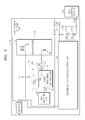
- FIG. 1 is a block diagram of an apparatus including a switching mode power supply (SMPS) according to an embodiment of the present general inventive concept;
- SMPS switching mode power supply
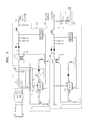
- FIG. 2 is a circuit diagram of a power blocking unit of FIG. 1 according to an embodiment of the present general inventive concept
- FIG. 3 is a circuit diagram of the SMPS of FIG. 1 according to an embodiment of the present general inventive concept
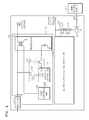
- FIG. 4 is a circuit diagram of a power blocking unit of FIG. 1 according to another embodiment of the present general inventive concept
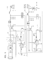
- FIG. 5 is a circuit diagram of the SMPS of FIG. 1 according to another embodiment of the present general inventive concept
- FIG. 6 is a block diagram of an apparatus including an auxiliary power unit and a SMPS according to another embodiment of the present general inventive concept
- FIG. 7 is a block diagram of an image forming apparatus including a SMPS according to an embodiment of the present general inventive concept
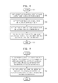
- FIG. 8 is a flowchart illustrating a method of supplying power using a switching mode power supply to supply power to an apparatus operable in an operation mode and a power savings mode;
- FIG. 9 is a flowchart illustrating a power supply method using a SMPS including two or more transformers according to an embodiment of the present general inventive concept.
- FIG. 1 is a block diagram of an apparatus 200 including a switching mode power supply (SMPS) 100 according to an exemplary embodiment of the present general inventive concept.
- the apparatus 200 is operable in an operation mode to perform one or more operations, and a power saving mode to reduce power consumption after the apparatus 200 does not perform an operation after a predetermined time period.
- the operations of the apparatus include, but are not limited to, scanning, printing, displaying, faxing, emailing, etc..
- the SMPS 100 includes a rectifier 110, a first output voltage unit 112, and a second output voltage unit 160.
- the first output voltage unit 112 includes a first switching unit 120, a first transformer 130, a first switching control unit 140 and a power blocking unit 150.
- the second output voltage unit 160 includes a second switching unit 161, a second transformer 162, and a second switching control unit 163.
- the apparatus 200 including the SMPS 100 may further include a main control module 210 that may control and/or determine various operations of the apparatus 200.
- the SMPS 100 and the apparatus 200 shown in FIG. 1 include elements relating to the present embodiment. Thus, it is obvious to one of ordinary skill in the art that the SMPS 100 and the apparatus 200 may further include general-purpose elements other than the elements shown in FIG. 1 .
- the apparatus 200 may include an image forming device, an image scanning device, a multi-function peripheral (MFP), a PC, a monitor, a facsimile, a TV, and the like. Further, the apparatus 200 is not limited thereto, and may be any apparatuses including the SMPS 100.
- MFP multi-function peripheral
- the main control module 210 may include a controller to operate the apparatus 200.
- the main control module 210 may include a microcomputer (MICOM) in electrical communication with the apparatus 200.
- MICOM microcomputer
- the description relating to the main control module 210 will be described in the power blocking unit 150 below.
- the SMPS 100 may include at least two transformers.
- the rectifier 110 rectifies an alternating current (AC) voltage.
- the rectifier 110 rectifies an applied AC voltage and outputs a direct current (DC) voltage.
- the DC voltage may, for example, be a high DC voltage having a voltage level greater than the applied AC voltage.
- the rectifier 110 may include a rectification element to rectify AC power and a planarization element to planarize the rectified power.
- the rectification element includes, but is not limited to, a bridge circuit constructed of diodes, and the planarization element may include, but is not limited to, a capacitor.
- the first switching unit 120 switches the voltage rectified by the rectifier 110 using the first transformer 130 so as to convert the rectified voltage into a first output voltage of the SMPS 100.
- the first output voltage may be, for example, a low DC voltage so as to operate a module other than the main control module 210 of the apparatus 200 including the SMPS 100.
- a low DC voltage corresponding to the first output voltage may include, but is not limited to, approximately 24 volts.
- the first transformer 130 transfers electrical energy from a circuit to another circuit according to an induction function of a coil.
- the first transformer 130 may transfer electrical energy applied to a first coil to second and third coils according to an operation of the first switching unit 120.
- the first coil of the first transformer 130 receives the voltage switched by the first switching unit 120 and transfers the switched voltage to the second and third coils.
- the first switching control unit 140 controls outputs a switching signal to control operation of the first switching unit 120. Accordingly, the first switching unit 120 generates the first output voltage in response to the switching control signal output from the first switching control unit 140.
- the first switching control unit 140 may include a power voltage terminal 141, a startup voltage terminal 142, , and a driving terminal 143. Accordingly, the first switching control unit 140 outputs a control signal from the driving terminal 143 to control the first switching unit 120.
- the first switching control unit 140 may include, but is not limited to, a pulse-width modulation (PWM) integrated circuit (IC).
- PWM pulse-width modulation
- the power blocking unit 150 blocks power supply to the startup terminal and the power voltage terminal of the first switching control unit 140 in the power saving mode.
- the main control module 210 when the apparatus 200 including the SMPS 100 is in the power saving mode, the main control module 210 outputs a signal indicating that the apparatus 200 is in the power saving mode.
- the power blocking unit 150 blocks power supply to the startup terminal 142 and the power voltage terminal 141 of the first switching control unit 140, by using the signal indicating that the apparatus 200 is in the power saving mode output from the main control module 210. Accordingly, when power to the startup terminal 142 and the power voltage terminal 141 is blocked, operation of the first switching unit 120 is halted, and output of the first output voltage is no longer generated.
- the power blocking unit 150 may include one, or more disconnection units 151, 152 to disconnect the startup terminal 142 and the power voltage terminal 141 1 from receiving power.
- the disconnection units 151, 152 may include, but are not limited to, at least one of a switch, transformer, relay, and photo coupler so as to block power supply to the startup terminal and the power voltage terminal of the first switching control unit 140, and may include any switching element to transfer a signal between electrically insulated circuits.
- the power blocking unit 150 may be in electrical communication with the first switching control unit 140 via one or more disconnection units 151,152 coupled to each of the startup terminal 142 and the power voltage terminal 141, as described in greater detail below.
- the disconnection units 151, 152 may disconnect the startup and power voltage terminals 142, 141 from receiving power. As a result, the signal output from the driving terminal 143 is halted, and the first output voltage is no longer generated.
- the detailed operation of the power blocking unit 150 is described in more detail below with reference to FIG. 2 .
- an SMPS 100 of at least one embodiment blocks power supply to the startup terminal 142 and the power voltage terminal 141 of the first switching control unit 140 in the power saving mode, thereby dramatically reducing standby power in the power saving mode.
- a conventional SMPS blocks a power voltage being supplied to a first switching control unit.
- a first switching unit does not operate, and the first switching control unit does not normally operate.
- the first switching control unit of the conventional SMPS compares the power voltage with a threshold voltage, when the power voltage of the first switching control unit is below the threshold voltage, the first switching control unit absorbs a startup current through a startup resistor connected to a startup terminal. Since the conventional SMPS blocks power supply to a power voltage terminal of the first switching control unit, although the first switching control unit does not continue operating even though the first switching control unit starts-up due to the startup current, a conduction loss occurs in the startup resistor.
- the power blocking unit 150 of the at least one exemplary embodiment of the present general inventive concept blocks the power supply to the startup terminal and the power voltage terminal of the first switching control unit 140 in the power saving mode, thereby preventing the conduction loss that occurs in the conventional SMPS.
- the conventional SMPS described above requires a comparator to compare the power voltage of the first switching control unit with a threshold voltage, a microcomputer unit to supply input power to the comparator, a transistor to block power supply to the first switching control unit, and the like, in order to reduce the standby power in the power saving mode, which causes an increase in the unit cost of the conventional SMPS.
- the SMPS 100 reduces the standby power in the power saving mode by using the power blocking unit 150, thereby preventing the unit cost of the SMPS 100 from increasing.
- the second output voltage unit 160 outputs a second output voltage of the SMPS 100 during the power saving mode using the second transformer 163. Accordingly, the second output voltage output by the second output voltage unit 160 may be used to operate the main control module 210 of the apparatus 200 including the SMPS 100.
- the power blocking unit 150 of the SMPS 100 blocks the power supply to the startup terminal and the power voltage terminal of the first switching control unit 140, although the first output voltage of the SM PS 100 is not output, the second output voltage output from the second output voltage unit 160 may still operate the main control module 210 of the apparatus 200.
- auxiliary power unit a battery, or the like may be used instead of the second output voltage unit 160 in order to guarantee the operation of the main control module 210 of the apparatus 200 according to conditions of use.
- the auxiliary power unit used to guarantee the operation of the main control module 210 of the apparatus 200 will be described in more detail with reference to FIG. 6 described further below.
- the second output voltage unit 160 includes the second switching unit 161, the second transformer 162, and the second switching control unit 163.
- the second switching unit 161 switches the voltage rectified by the rectifier 110 using the second transformer 162 so as to convert the rectified voltage into the second output voltage of the SMPS 100.
- the second output voltage may be, for example, a low DC voltage so as to operate the main control module 210 of the apparatus 200 including the SMPS 100.
- a low DC voltage corresponding to the second output voltage may be, but is not limited to, approximately 5 volts and approximately 3.3 volts.
- the second transformer 162 transfers electrical energy from a first circuit to a second circuit according to an induction characteristic of a coil included in the second transformer 162.
- the second transformer 162 may transfer electrical energy applied to a first coil to second and third coils according to an operation of the second switching unit 161.
- the second switching control unit 163 controls the second switching unit 161.
- the second switching control unit 163 may include a power voltage terminal 141, a start-up voltage terminal 142, , and a driving terminal 143. Accordingly, the second switching control unit 162 controls the second switching unit 161 by using a signal output from the driving terminal 143.
- the second switching control unit 163 may include, but is not limited to, a PWM integrated circuit (IC).
- IC PWM integrated circuit
- the SMPS 100 guarantees the operation of the main control module 210 using the second output voltage unit 160.
- the power blocking unit 150 blocks power supply to the startup terminal and the power voltage terminal of the first switching control unit 140, and thus the switching operation of the first switching unit 120 stops, thereby reducing standby power in the power saving mode.
- FIG. 2 is a circuit diagram of the power blocking unit 150 of FIG. 1 according to an exemplary embodiment of the present general inventive concept.
- the first switching control unit 140 includes a power voltage terminal 141, a startup voltage terminal 142, and a driving terminal 143.
- the power blocking unit 150 includes a first light receiving unit 151 and a second light receiving unit 152.
- the first and second light receiving units 151, 152 respond to respectively first and second light emitting units 221, 222, as discussed in greater detail below.
- a light emitting module 220 includes a first light emitting unit 221 and a second light emitting unit 222.
- the first light emitting unit 221 controls the first light receiving unit 151.
- the second light emitting unit 222 controls the second light receiving unit 152.
- the light emitting module 220 may include, but is not limited to, a photo coupler, that includes the light receiving units 151, 152 and the light emitting units 221, 222.
- the light receiving units 151, 152 and the light emitting units 221, 222 are electrically insulated from each other.
- the light emitting units 221, 222 do not emit light, and thus the light receiving units 151, 152 are electrically insulated from each other, and are opened, thereby disconnecting the power voltage terminal 141 and the startup voltage terminal 142.
- the light emitting units 221, 222 When current flows to the light emitting units 221, 222, the light emitting units emit light 221, 222, and thus the light receiving units 151, 152 are shorted.
- the light receiving units being opened means that the light receiving units are powered off.
- the light receiving units being shorted means that the light receiving units are powered on. Operation of a photo coupler is obvious to one of ordinary skill in the art, and thus a detailed description thereof will not be given here.
- the first light receiving unit 151 may block power supply to the power voltage terminal 141 of the first switching control unit 140.
- the second light receiving unit 152 may block power supply to the startup voltage terminal 142 of the first switching control unit 140.
- the first light emitting unit 221 may block power supply to the power voltage terminal 141 of the first switching control unit 140 by using the first light receiving unit 151.
- the second light emitting unit 222 may block power supply to the startup voltage terminal 142 of the first switching control unit 140 by using the second light receiving unit 152.
- the main control module 210 when the apparatus 200 is not in the power saving mode (hereinafter, referred to as an operation mode), the main control module 210 applies a first signal to a power saving signal pin 225, and, when the apparatus 200 is in the power saving mode, the main control module 210 applies a second signal to the power saving signal pin 225.
- the first signal may be a low power signal
- the second signal may be a high power signal.
- the power saving signal pin 225 is connected to the SMPS 100, and may be included in the apparatus 200 including the SMPS 100, but is not limited thereto, and may be included in the SMPS 100.
- the main control module 210 applies the first signal to the power saving signal pin 225. If the first signal is applied to the power saving signal pin 225, current flows to the first light emitting unit 221 and the second light emitting unit 222. Thus, when the first light emitting unit 221 and the second light emitting unit 222 emit light, the first light receiving unit 151 and the second light receiving unit 152 are shorted. Accordingly, in at least one exemplary embodiment, when the apparatus 200 is in the operation mode, the SMPS 100 may output both the first output voltage and the second output voltage.
- the main control module 210 applies the second signal to the power saving signal pin 225. If the second signal is applied to the power saving signal pin 225, current does not flow to the first light emitting unit 221 and the second light emitting unit 222. Thus, when the first light emitting unit 221 and the second light emitting unit 222 do not emit light, the first light receiving unit 151 and the second light receiving unit 152 are opened. Thus, when the apparatus 200 is in the power saving mode, the power blocking unit 150 blocks power supply to the power voltage terminal 141 and the startup voltage terminal 142 of the first switching control unit 140. Accordingly, in at least one exemplary embodiment, the SMPS 100 halts the operation of the first switching control unit 140 and outputs only the second output voltage during the power saving mode.
- the SMPS 100 shown in FIG. 2 is merely an exemplary embodiment and the present general inventive concept is not limited thereto.
- the power saving signal pin 225 is included in the SMPS 100 in at least one exemplary embodiment for descriptive convenience, the present general inventive concept is not limited thereto.
- a photo coupler may be used as the power blocking unit 150 in the present embodiment, the present general inventive concept is not limited thereto. It is obvious to one of ordinary skill in the art that at least one of a transformer, a switch, and/or a relay may be used as the power blocking unit 150 as described above.
- FIG. 3 is a circuit diagram of the SMPS 100 according to an exemplary embodiment of the present general inventive concept.
- the operation principle of a circuit shown in FIG. 3 is obvious to one of ordinary skill in the art with reference to FIGS. 1 and 2 , and thus a detailed description thereof will not be repeated here.
- the SMPS 100 blocks power supply to the power voltage terminal and the startup voltage terminal of the first switching control unit 140 so that the operations of the first switching unit 120 and the first switching control unit 140 are halted, thereby reducing standby power loss.
- an SMPS 100 blocks power supply to the power voltage terminal and the startup voltage terminal of the first switching control unit 140, resulting in a reduction of power consumption to approximately 0.13 Watt during the power saving mode.
- FIG. 4 is a circuit diagram of the power blocking unit 150 of FIG. 1 according to another exemplary embodiment of the present general inventive concept. Referring to FIG. 4 , FIGS. 2 and 4 are the same except that a transistor 230 is further included in the power blocking unit 150, and thus redundant descriptions will not be repeated here.
- the power blocking unit 150 of at least one exemplary embodiment includes light receiving units 151 and 152 of a photo coupler that are controlled by the main control module 210.
- the main control module 210 when the apparatus 200 is in the power saving mode, the main control module 210 outputs a signal indicating that the apparatus 200 is in the power saving mode.
- the output signal is input to the transistor 230 through the power saving signal pin 225.
- the transistor 230 switches a signal input to the light emitting module 220 by using the signal indicating that the apparatus 200 is in the power saving mode output from the main control module 210.
- the power saving signal pin 225 and the transistor 230 of at least one exemplary embodiment may be included in the apparatus 200 including the SMPS 100, but is not limited thereto, and may be included in the SMPS 100.
- the main control module 210 applies a first signal to the power saving signal pin 225. If the first signal is applied to the power saving signal pin 225, the transistor 230 is powered on, and thus current flows to the first light emitting unit 221 and the second light emitting unit 222. Thus, when the first light emitting unit 221 and the second light emitting unit 222 emit light, the first light receiving unit 151 and the second light receiving unit 152 are shorted. Accordingly at least one exemplary embodiment provides that, when the apparatus 200 is in the operation mode, the SMPS 100 outputs both the first output voltage and the second output voltage.
- the main control module 210 applies a second signal to the power saving signal pin 225. If the second signal is applied to the power saving signal pin 225, the transistor 230 is powered off, and thus, current does not flow to the first light emitting unit 221 and the second light emitting unit 222.
- the first signal applied to the power saving pin 225 may be a high signal
- the second signal may be a low signal having a signal level being lower than the high signal.
- the power blocking unit 150 blocks power supply to the power voltage terminal and the startup voltage terminal of the first switching control unit 140.
- at least one exemplary embodiment of the present general inventive concept provides a SMPS 100 that halts operation of the first switching control unit 140 and outputs only the second output voltage in the power saving mode.
- the apparatus 200 including the SMPS 100 further includes the transistor 230, thereby reducing current consumption and implementing a stable operation.
- FIG. 5 is a circuit diagram of the SMPS 100 according to another exemplary embodiment of the present general inventive concept. Referring to FIG. 5 , FIGS. 3 through 5 are the same except that the first switching control unit 140 does not include a startup voltage terminal, and thus redundant descriptions will not be repeated here.
- the first switching control unit 140 of the SMPS 100 of at least one exemplary embodiment does not include a startup voltage terminal 142.
- the power voltage terminal 141 of the first switching control unit 140 is connected to a power voltage terminal 1631 of the second switching control unit 163.
- Power is supplied to a startup voltage terminal 1632 of the second switching control unit 163 so that the second switching control unit 163 can operate, and thus power can be supplied to the power voltage terminal 141 of the first switching control unit 140 connected to the power voltage terminal 1631 of the second switching control unit 163.
- the power blocking unit 150 blocks power supply to the power voltage terminal 141 of the first switching control unit 140 in the power saving mode.
- the power blocking unit 150 is a photo coupler, for example, the power blocking unit 150 may include the first light receiving unit 151 of the photo coupler that blocks power supply to the power voltage terminal 141 of the first switching control unit 140.
- the light emitting module 220 may include the first light emitting unit 221 that controls the first light receiving unit 151.
- the power blocking unit 150 blocks power supply to the power voltage terminal 141 of the first switching control unit 140 during the power saving mode, thereby reducing power consumption.
- FIG. 6 is a block diagram of an apparatus including an auxiliary power unit 240 and a SMPS 100 according to another exemplary embodiment of the present general inventive concept. Referring to FIG. 6 , FIGS. 3 through 6 are the same except that the apparatus further includes the auxiliary power unit 240 and an auxiliary power blocking unit 170 and does not include the second output voltage unit 160, and thus redundant descriptions will not be repeated here.
- the first switching unit 120 converts a voltage rectified by the rectifier 110 into a first output voltage, a second output voltage, and a charge voltage using the first transformer 130.
- the first output voltage may be used to operate a control module other than the main control module 210 of the apparatus 200, and the second output voltage may be used to operate the main control module 210 of the apparatus 200.
- the charging voltage may be used to charge the auxiliary power unit 240.
- the auxiliary power unit 240 may be charged by the charging voltage converted in the first transformer 130 under the control of the first switching unit 120.
- the auxiliary power unit 240 of at least one exemplary embodiment may include, but is not limited to, a battery and a capacitor.
- the auxiliary power blocking unit 170 electrically separates the auxiliary power unit 240 from the SMPS 100 in a power saving mode.
- the auxiliary power blocking unit 170 of at least one exemplary embodiment includes, but is not limited to, a transistor 171 and a p-type metal oxide semiconductor field effect transistor (PMOSFET) 172.
- PMOSFET p-type metal oxide semiconductor field effect transistor
- the main control module 210 applies a first signal to a first power saving signal pin 159 and the second power saving signal pin 225.
- the auxiliary power unit 240 is connected to the SMPS 100.
- the SMPS 100 If the first signal is applied to the second power saving signal pin 225, the transistor 171 is powered on, and the first light receiving unit 151 and the second light receiving unit 152 are powered on. Thus, when the apparatus 200 is in the operation mode, the SMPS 100 outputs the first output voltage and the charging voltage. Accordingly, the auxiliary power unit 240 may be charged by the charging voltage output by the SMPS 100.
- the main control module 210 applies a second signal to the first power saving signal pin 159 and the second power saving signal pin 225.
- the auxiliary power blocking unit 170 electrically separates the auxiliary power unit 240 from the SMPS 100.
- the auxiliary power unit 240 may be electrically separated, i.e., disconnected, from the SMPS 100.
- the first signal output by the main control module 220 may be a high signal
- the second signal may be a low signal having a voltage level being lower than the high signal.
- the power blocking unit 150 blocks power supply to the power voltage terminal and the startup voltage terminal of the first switching control unit 140.
- the operation of the first switching control unit 140 is stopped during the power saving mode, so that the SMPS 100 does not output the first output voltage and the second output voltage, whereas the operation of the SMPS 100 can be guaranteed in the power saving mode by the previously charged auxiliary power unit 240.
- FIG. 7 is a block diagram of an image forming apparatus 700 including the SMPS 100 according to an exemplary embodiment of the present general inventive concept.
- the image forming apparatus 700 includes the SMPS 100, the main control module 210, a communication interface unit 710, a user interface unit 720, a storage unit 730, an image forming unit 740, a fax unit 750, and a transmission function performing unit 760.
- the SMPS 100 includes a first voltage output unit 112 having a first transformer 130, and a second output voltage unit 160 having a second transformer 162.
- the first voltage output unit 112 receives an input voltage to generate a first output voltage through the first transformer 130 in an operation mode.
- the operation mode is switched to a power saving mode, the first voltage output unit stops generating the first output voltage through the first transformer 130.
- the second voltage output unit 160 receives the first input voltage, and outputs a second output voltage through a second transformer 162 in both the operation mode and in the power saving mode.
- the communication interface unit 710 may transmit and/or receive data to and/or from an external apparatus over a network.
- the communication interface unit 710 of at least one exemplary embodiment includes, but is not limited to, a modem used to transmit and receive data via fax, a network module used to access the network, a universal serial bus (USB) host module used to form a data movement channel with a portable storage medium, and the like according to functions of the image forming apparatus 700.
- the external apparatus may be connected to the image forming apparatus 700 over a wired or wireless network.
- the external apparatus may include, but is not limited to a computer system, a mobile terminal, a power digital assistant (PDA), a server, or the like.
- PDA power digital assistant
- the user interface unit 720 may obtain an input signal from a user, and may also display information to the user.
- the user interface unit 720 includes all input and output devices such as a display panel, a mouse, a keyboard, a touch screen, a monitor, and a speaker disposed in the image forming apparatus 700.
- the storage unit 730 stores data including, but not limited to, printing data, scan data, and the like, which may be generated during the operation of the image forming apparatus 700.
- the image forming unit 740 forms an image of printing data that is to be printed.
- the fax unit 750 transmits and receives fax data that is to be faxed.
- the transmission function performing unit 760 transmits a document that is to be transmitted to the external apparatus such as the server, the portable storage medium, the computer system, or the like.
- the image forming apparatus 700 of at lest one exemplary embodiment may be an example of the apparatus 200.
- the main control module 210 outputs a signal indicating that the image forming apparatus 700 is in the power saving mode and/or a power blocking signal in response to determining the image forming apparatus 700 has entered the power saving mode.
- the SMPS 100 blocks power supply to a startup terminal and a power voltage terminal of a switching control unit that controls switching of a voltage that is input to a transformer of the SMPS 100 by using the signal indicating that the image forming apparatus 700 is in the power saving mode and/or the power blocking signal.
- FIG. 8 is a flowchart illustrating a method of supplying power using a switching mode power supply to supply power to an apparatus operable in an operation mode and a power savings mode.
- the method begins at operation 800, and proceeds to operation 802 where a first voltage output unit outputs a first output voltage from during the operation mode.
- a power saving mode is detected, and a power blocking signal is output n response to detecting the power savings mode.
- output of the first output voltage generated by the first voltage output unit is halted in response to the power blocking signal.
- a second output voltage from a second voltage output unit is output, while output of the first output voltage is halted during the power saving mode, and the method ends at operation 810.
- At least one exemplary embodiment of Applicant's teachings provides that, although the first output voltage of the SMPS 100 is halted, i.e. not output, when an apparatus 200 is in the power saving mode, the second output voltage output from the second output voltage unit 160 may be utilized to operate various devices, including but not limited to, a main control module 210 of the apparatus 200.
- FIG. 9 is a flowchart illustrating a power supply method using the SMPS 100 including two or more transformers according to an exemplary embodiment of the present general inventive concept.
- the power supply method includes operations that are time serially processed in the SMPS 100, the apparatus 200 and the image forming apparatus 700 shown in FIGS. 1 through 7 .
- the description of the SMPS 100, the apparatus 200 and the image forming apparatus 700 shown in FIGS. 1 through 7 may be applied to the power supply method of FIG. 9 .
- the power blocking unit 150 of the SMPS 100 blocks power supply to a startup voltage terminal and a power voltage terminal of the first switching control unit 140 that controls switching of a voltage input to the first transformer 130.
- the second output voltage unit 160 outputs an output voltage to operate the main control module 210 of the apparatus 200 including the SMPS 100 using the second transformer 162.
- the SMPS 100 of at least one exemplary embodiment can reduce power consumption in a power saving mode.
- the present general inventive concept can also be implemented as computer-readable code on a computer-readable recording medium.
- the computer-readable recording medium is any data storage device that can store data which can be thereafter read by a computer system. Examples of the computer-readable recording medium include read-only memory (ROM), random-access memory (RAM), CD-ROMs, magnetic tapes, floppy disks, optical data storage devices, etc.
- the power consumption of a SMPS 100 can be reduced during a power saving mode. Furthermore, the number of elements used included with the SMPS 100 is reduced, thereby reducing manufacturing costs of the SMPS 100.
Landscapes
- Engineering & Computer Science (AREA)
- Theoretical Computer Science (AREA)
- Power Engineering (AREA)
- Physics & Mathematics (AREA)
- General Engineering & Computer Science (AREA)
- General Physics & Mathematics (AREA)
- Dc-Dc Converters (AREA)
- Direct Current Feeding And Distribution (AREA)
Abstract
Description
- This application claims priority under 35 U.S.C. §119(a) from Korean Patent Application No.
10-2010-0053029, filed on June 4, 2010 - The present general inventive concept relates to a switching mode power supply (SMPS) and a power supply method using the SMPS.
- A switching mode power supply (SMPS) may be used as an apparatus for supplying power to electronic products. The SMPS converts input alternating current (AC) voltages and outputs static voltages to operate electronic products. When electronic products stand by for a predetermined period of time, electronic products enter a power saving mode. Electronic products need to guarantee partial functionality while in the power saving mode, and thus the SMPS does not entirely stop operating. Regulations for standby power of electronic products have been recently strengthened in order to reduce amounts of carbon dioxide globally, and thus a method of reducing power consumption of a SMPS in a power saving mode is needed.
- The present general inventive concept provides a power supply method using a switching mode power supply (SMPS) in a power saving mode and a SMPS to perform the method.
- Additional features and utilities of the present general inventive concept will be set forth in part in the description which follows and, in part, will be obvious from the description, or may be learned by practice of the present general inventive concept.
- The present general inventive concept also provides a computer readable recording medium storing a program to execute the method.
- According to feature of the present general inventive concept, there is provided an image forming apparatus including a switching mode power supply (SMPS) including at least two transformers, the SMPS including: a rectifier to rectify an alternating current (AC) voltage; a first switching unit to switch the voltage rectified by the rectifier using a first transformer from among the at least two transformers so as to convert the rectified voltage into a first output voltage of the SMPS; a first switching control unit to control the first switching unit; and a power blocking unit to block power supply to a startup voltage terminal and a power voltage terminal of the first switching control unit in a power saving mode.
- According to another feature of the present general inventive concept, there is provided a power supply method using a switching mode power supply (SMPS) including at least two transformers, the method including: blocking power supply to a startup voltage terminal and a power voltage terminal of a switching control unit to control switching of a voltage input to a first transformer from among the at least two transformers in a power saving mode; and outputting an output voltage to operate a main control module of an apparatus including the SMPS in the power saving mode using a second transformer from among the at least two transformers.
- According to another feature of the present general inventive concept, there is provided a computer readable recording medium storing a program to execute a method.
- The above and other features and advantages of the present general inventive concept will become more apparent by describing in detail exemplary embodiments thereof with reference to the attached drawings in which:
-
FIG. 1 is a block diagram of an apparatus including a switching mode power supply (SMPS) according to an embodiment of the present general inventive concept; -
FIG. 2 is a circuit diagram of a power blocking unit ofFIG. 1 according to an embodiment of the present general inventive concept; -
FIG. 3 is a circuit diagram of the SMPS ofFIG. 1 according to an embodiment of the present general inventive concept; -
FIG. 4 is a circuit diagram of a power blocking unit ofFIG. 1 according to another embodiment of the present general inventive concept; -
FIG. 5 is a circuit diagram of the SMPS ofFIG. 1 according to another embodiment of the present general inventive concept; -
FIG. 6 is a block diagram of an apparatus including an auxiliary power unit and a SMPS according to another embodiment of the present general inventive concept; -
FIG. 7 is a block diagram of an image forming apparatus including a SMPS according to an embodiment of the present general inventive concept; -
FIG. 8 is a flowchart illustrating a method of supplying power using a switching mode power supply to supply power to an apparatus operable in an operation mode and a power savings mode; and -
FIG. 9 is a flowchart illustrating a power supply method using a SMPS including two or more transformers according to an embodiment of the present general inventive concept. - Reference will now be made in detail to exemplary embodiments of the present general inventive concept, examples of which are illustrated in the accompanying drawings, wherein like reference numerals refer to the like elements throughout. The exemplary embodiments are described below in order to explain the present general inventive concept by referring to the figures.
-
FIG. 1 is a block diagram of anapparatus 200 including a switching mode power supply (SMPS) 100 according to an exemplary embodiment of the present general inventive concept. Theapparatus 200 is operable in an operation mode to perform one or more operations, and a power saving mode to reduce power consumption after theapparatus 200 does not perform an operation after a predetermined time period. The operations of the apparatus include, but are not limited to, scanning, printing, displaying, faxing, emailing, etc.. Referring toFIG. 1 , theSMPS 100 includes arectifier 110, a firstoutput voltage unit 112, and a secondoutput voltage unit 160. The firstoutput voltage unit 112 includes afirst switching unit 120, afirst transformer 130, a firstswitching control unit 140 and apower blocking unit 150. The secondoutput voltage unit 160 includes asecond switching unit 161, asecond transformer 162, and a secondswitching control unit 163. Theapparatus 200 including the SMPS 100 may further include amain control module 210 that may control and/or determine various operations of theapparatus 200. - The SMPS 100 and the
apparatus 200 shown inFIG. 1 include elements relating to the present embodiment. Thus, it is obvious to one of ordinary skill in the art that theSMPS 100 and theapparatus 200 may further include general-purpose elements other than the elements shown inFIG. 1 . - The
apparatus 200 may include an image forming device, an image scanning device, a multi-function peripheral (MFP), a PC, a monitor, a facsimile, a TV, and the like. Further, theapparatus 200 is not limited thereto, and may be any apparatuses including theSMPS 100. - The
main control module 210 may include a controller to operate theapparatus 200. Themain control module 210 may include a microcomputer (MICOM) in electrical communication with theapparatus 200. The description relating to themain control module 210 will be described in thepower blocking unit 150 below. - The SMPS 100 according to an exemplary embodiment of the present general inventive concept may include at least two transformers.
- The
rectifier 110 rectifies an alternating current (AC) voltage. In more detail, therectifier 110 rectifies an applied AC voltage and outputs a direct current (DC) voltage. The DC voltage may, for example, be a high DC voltage having a voltage level greater than the applied AC voltage. - For example, the
rectifier 110 may include a rectification element to rectify AC power and a planarization element to planarize the rectified power. The rectification element includes, but is not limited to, a bridge circuit constructed of diodes, and the planarization element may include, but is not limited to, a capacitor. - The
first switching unit 120 switches the voltage rectified by therectifier 110 using thefirst transformer 130 so as to convert the rectified voltage into a first output voltage of theSMPS 100. The first output voltage may be, for example, a low DC voltage so as to operate a module other than themain control module 210 of theapparatus 200 including theSMPS 100. In at least one exemplary embodiment, a low DC voltage corresponding to the first output voltage may include, but is not limited to, approximately 24 volts. - The first transformer 130 transfers electrical energy from a circuit to another circuit according to an induction function of a coil. For example, the
first transformer 130 may transfer electrical energy applied to a first coil to second and third coils according to an operation of thefirst switching unit 120. Thus, the first coil of thefirst transformer 130 receives the voltage switched by thefirst switching unit 120 and transfers the switched voltage to the second and third coils. - The first
switching control unit 140 controls outputs a switching signal to control operation of thefirst switching unit 120. Accordingly, thefirst switching unit 120 generates the first output voltage in response to the switching control signal output from the firstswitching control unit 140. The firstswitching control unit 140 may include apower voltage terminal 141, astartup voltage terminal 142, , and adriving terminal 143. Accordingly, the firstswitching control unit 140 outputs a control signal from thedriving terminal 143 to control thefirst switching unit 120. - For example, the first
switching control unit 140 may include, but is not limited to, a pulse-width modulation (PWM) integrated circuit (IC). - The
power blocking unit 150 blocks power supply to the startup terminal and the power voltage terminal of the firstswitching control unit 140 in the power saving mode. - For example, when the
apparatus 200 including theSMPS 100 is in the power saving mode, themain control module 210 outputs a signal indicating that theapparatus 200 is in the power saving mode. Thepower blocking unit 150 blocks power supply to thestartup terminal 142 and thepower voltage terminal 141 of the firstswitching control unit 140, by using the signal indicating that theapparatus 200 is in the power saving mode output from themain control module 210. Accordingly, when power to thestartup terminal 142 and thepower voltage terminal 141 is blocked, operation of thefirst switching unit 120 is halted, and output of the first output voltage is no longer generated. - The
power blocking unit 150 may include one, ormore disconnection units startup terminal 142 and thepower voltage terminal 141 1 from receiving power. Thedisconnection units switching control unit 140, and may include any switching element to transfer a signal between electrically insulated circuits. For example, thepower blocking unit 150 may be in electrical communication with the firstswitching control unit 140 via one or more disconnection units 151,152 coupled to each of thestartup terminal 142 and thepower voltage terminal 141, as described in greater detail below. Accordingly, thedisconnection units power voltage terminals terminal 143 is halted, and the first output voltage is no longer generated. The detailed operation of thepower blocking unit 150 is described in more detail below with reference toFIG. 2 . - As discussed above, an
SMPS 100 of at least one embodiment blocks power supply to thestartup terminal 142 and thepower voltage terminal 141 of the firstswitching control unit 140 in the power saving mode, thereby dramatically reducing standby power in the power saving mode. - A conventional SMPS blocks a power voltage being supplied to a first switching control unit. In the conventional case, a first switching unit does not operate, and the first switching control unit does not normally operate. Further, the first switching control unit of the conventional SMPS compares the power voltage with a threshold voltage, when the power voltage of the first switching control unit is below the threshold voltage, the first switching control unit absorbs a startup current through a startup resistor connected to a startup terminal. Since the conventional SMPS blocks power supply to a power voltage terminal of the first switching control unit, although the first switching control unit does not continue operating even though the first switching control unit starts-up due to the startup current, a conduction loss occurs in the startup resistor.
- Unlike the conventional SMPS, the
power blocking unit 150 of the at least one exemplary embodiment of the present general inventive concept blocks the power supply to the startup terminal and the power voltage terminal of the firstswitching control unit 140 in the power saving mode, thereby preventing the conduction loss that occurs in the conventional SMPS. - Further, the conventional SMPS described above requires a comparator to compare the power voltage of the first switching control unit with a threshold voltage, a microcomputer unit to supply input power to the comparator, a transistor to block power supply to the first switching control unit, and the like, in order to reduce the standby power in the power saving mode, which causes an increase in the unit cost of the conventional SMPS.
- However, the
SMPS 100 according to at least one exemplary embodiment of the present general inventive concept reduces the standby power in the power saving mode by using thepower blocking unit 150, thereby preventing the unit cost of theSMPS 100 from increasing. - Referring again to
FIG. 1 , the secondoutput voltage unit 160 outputs a second output voltage of theSMPS 100 during the power saving mode using thesecond transformer 163. Accordingly, the second output voltage output by the secondoutput voltage unit 160 may be used to operate themain control module 210 of theapparatus 200 including theSMPS 100. - Thus, when the
apparatus 200 is in the power saving mode, since thepower blocking unit 150 of theSMPS 100 blocks the power supply to the startup terminal and the power voltage terminal of the firstswitching control unit 140, although the first output voltage of theSM PS 100 is not output, the second output voltage output from the secondoutput voltage unit 160 may still operate themain control module 210 of theapparatus 200. - However, it will be understood by one of ordinary skill in the art that an auxiliary power unit, a battery, or the like may be used instead of the second
output voltage unit 160 in order to guarantee the operation of themain control module 210 of theapparatus 200 according to conditions of use. The auxiliary power unit used to guarantee the operation of themain control module 210 of theapparatus 200 will be described in more detail with reference toFIG. 6 described further below. - The second
output voltage unit 160 includes thesecond switching unit 161, thesecond transformer 162, and the secondswitching control unit 163. - The
second switching unit 161 switches the voltage rectified by therectifier 110 using thesecond transformer 162 so as to convert the rectified voltage into the second output voltage of theSMPS 100. The second output voltage may be, for example, a low DC voltage so as to operate themain control module 210 of theapparatus 200 including theSMPS 100. In at least one exemplary embodiment of the present general inventive concept, a low DC voltage corresponding to the second output voltage may be, but is not limited to, approximately 5 volts and approximately 3.3 volts. - The
second transformer 162 transfers electrical energy from a first circuit to a second circuit according to an induction characteristic of a coil included in thesecond transformer 162. For example, thesecond transformer 162 may transfer electrical energy applied to a first coil to second and third coils according to an operation of thesecond switching unit 161. - The second
switching control unit 163 controls thesecond switching unit 161. The secondswitching control unit 163 may include apower voltage terminal 141, a start-upvoltage terminal 142, , and a drivingterminal 143. Accordingly, the secondswitching control unit 162 controls thesecond switching unit 161 by using a signal output from the drivingterminal 143. - For example, the second
switching control unit 163 may include, but is not limited to, a PWM integrated circuit (IC). - Therefore, when the
apparatus 200 is in the power saving mode, theSMPS 100 guarantees the operation of themain control module 210 using the secondoutput voltage unit 160. Thepower blocking unit 150 blocks power supply to the startup terminal and the power voltage terminal of the firstswitching control unit 140, and thus the switching operation of thefirst switching unit 120 stops, thereby reducing standby power in the power saving mode. -
FIG. 2 is a circuit diagram of thepower blocking unit 150 ofFIG. 1 according to an exemplary embodiment of the present general inventive concept. Referring toFIG. 2 , the firstswitching control unit 140 includes apower voltage terminal 141, astartup voltage terminal 142, and a drivingterminal 143. Thepower blocking unit 150 includes a firstlight receiving unit 151 and a secondlight receiving unit 152. The first and secondlight receiving units light emitting units - A
light emitting module 220 includes a firstlight emitting unit 221 and a secondlight emitting unit 222. The firstlight emitting unit 221 controls the firstlight receiving unit 151. The secondlight emitting unit 222 controls the secondlight receiving unit 152. Further, thelight emitting module 220 may include, but is not limited to, a photo coupler, that includes thelight receiving units light emitting units - The
light receiving units light emitting units light emitting units light emitting units light receiving units power voltage terminal 141 and thestartup voltage terminal 142. When current flows to thelight emitting units light receiving units - The first
light receiving unit 151 may block power supply to thepower voltage terminal 141 of the firstswitching control unit 140. The secondlight receiving unit 152 may block power supply to thestartup voltage terminal 142 of the firstswitching control unit 140. The firstlight emitting unit 221 may block power supply to thepower voltage terminal 141 of the firstswitching control unit 140 by using the firstlight receiving unit 151. The secondlight emitting unit 222 may block power supply to thestartup voltage terminal 142 of the firstswitching control unit 140 by using the secondlight receiving unit 152. - With respect to the
light emitting module 220, when theapparatus 200 is not in the power saving mode (hereinafter, referred to as an operation mode), themain control module 210 applies a first signal to a power savingsignal pin 225, and, when theapparatus 200 is in the power saving mode, themain control module 210 applies a second signal to the power savingsignal pin 225. For example, the first signal may be a low power signal, and the second signal may be a high power signal. The powersaving signal pin 225 is connected to theSMPS 100, and may be included in theapparatus 200 including theSMPS 100, but is not limited thereto, and may be included in theSMPS 100. - When the
apparatus 200 is in the operation mode, for example, themain control module 210 applies the first signal to the power savingsignal pin 225. If the first signal is applied to the power savingsignal pin 225, current flows to the firstlight emitting unit 221 and the secondlight emitting unit 222. Thus, when the firstlight emitting unit 221 and the secondlight emitting unit 222 emit light, the firstlight receiving unit 151 and the secondlight receiving unit 152 are shorted. Accordingly, in at least one exemplary embodiment, when theapparatus 200 is in the operation mode, theSMPS 100 may output both the first output voltage and the second output voltage. - When the
apparatus 200 is in the power saving mode, for example, themain control module 210 applies the second signal to the power savingsignal pin 225. If the second signal is applied to the power savingsignal pin 225, current does not flow to the firstlight emitting unit 221 and the secondlight emitting unit 222. Thus, when the firstlight emitting unit 221 and the secondlight emitting unit 222 do not emit light, the firstlight receiving unit 151 and the secondlight receiving unit 152 are opened. Thus, when theapparatus 200 is in the power saving mode, thepower blocking unit 150 blocks power supply to thepower voltage terminal 141 and thestartup voltage terminal 142 of the firstswitching control unit 140. Accordingly, in at least one exemplary embodiment, theSMPS 100 halts the operation of the firstswitching control unit 140 and outputs only the second output voltage during the power saving mode. - The
SMPS 100 shown inFIG. 2 is merely an exemplary embodiment and the present general inventive concept is not limited thereto. Although the power savingsignal pin 225 is included in theSMPS 100 in at least one exemplary embodiment for descriptive convenience, the present general inventive concept is not limited thereto. - Although a photo coupler may be used as the
power blocking unit 150 in the present embodiment, the present general inventive concept is not limited thereto. It is obvious to one of ordinary skill in the art that at least one of a transformer, a switch, and/or a relay may be used as thepower blocking unit 150 as described above. -
FIG. 3 is a circuit diagram of theSMPS 100 according to an exemplary embodiment of the present general inventive concept. The operation principle of a circuit shown inFIG. 3 is obvious to one of ordinary skill in the art with reference toFIGS. 1 and2 , and thus a detailed description thereof will not be repeated here. - With reference to a conventional SMPS, when an
output end 300 that outputs a first output voltage in a power saving mode is insulated, thefirst switching unit 120 and the firstswitching control unit 140 normally operate, which causes standby power loss. - However, the
SMPS 100 according to exemplary embodiments of the present general inventive concept blocks power supply to the power voltage terminal and the startup voltage terminal of the firstswitching control unit 140 so that the operations of thefirst switching unit 120 and the firstswitching control unit 140 are halted, thereby reducing standby power loss. For example, anSMPS 100 according to at least one exemplary embodiment blocks power supply to the power voltage terminal and the startup voltage terminal of the firstswitching control unit 140, resulting in a reduction of power consumption to approximately 0.13 Watt during the power saving mode. -
FIG. 4 is a circuit diagram of thepower blocking unit 150 ofFIG. 1 according to another exemplary embodiment of the present general inventive concept. Referring toFIG. 4 ,FIGS. 2 and4 are the same except that atransistor 230 is further included in thepower blocking unit 150, and thus redundant descriptions will not be repeated here. - The
power blocking unit 150 of at least one exemplary embodiment includeslight receiving units main control module 210. - For example, when the
apparatus 200 is in the power saving mode, themain control module 210 outputs a signal indicating that theapparatus 200 is in the power saving mode. The output signal is input to thetransistor 230 through the power savingsignal pin 225. - The
transistor 230 switches a signal input to thelight emitting module 220 by using the signal indicating that theapparatus 200 is in the power saving mode output from themain control module 210. The powersaving signal pin 225 and thetransistor 230 of at least one exemplary embodiment may be included in theapparatus 200 including theSMPS 100, but is not limited thereto, and may be included in theSMPS 100. - When the
apparatus 200 is in the operation mode, for example, themain control module 210 applies a first signal to the power savingsignal pin 225. If the first signal is applied to the power savingsignal pin 225, thetransistor 230 is powered on, and thus current flows to the firstlight emitting unit 221 and the secondlight emitting unit 222. Thus, when the firstlight emitting unit 221 and the secondlight emitting unit 222 emit light, the firstlight receiving unit 151 and the secondlight receiving unit 152 are shorted. Accordingly at least one exemplary embodiment provides that, when theapparatus 200 is in the operation mode, theSMPS 100 outputs both the first output voltage and the second output voltage. - When the
apparatus 200 is in the power saving mode, for example, themain control module 210 applies a second signal to the power savingsignal pin 225. If the second signal is applied to the power savingsignal pin 225, thetransistor 230 is powered off, and thus, current does not flow to the firstlight emitting unit 221 and the secondlight emitting unit 222. It can be appreciated that, for example, the first signal applied to thepower saving pin 225 may be a high signal, and the second signal may be a low signal having a signal level being lower than the high signal. Thus, when the firstlight emitting unit 221 and the secondlight emitting unit 222 do not emit light, the firstlight receiving unit 151 and the secondlight receiving unit 152 are opened (powered off). Accordingly, when theapparatus 200 is in the power saving mode, thepower blocking unit 150 blocks power supply to the power voltage terminal and the startup voltage terminal of the firstswitching control unit 140. As a result, at least one exemplary embodiment of the present general inventive concept provides aSMPS 100 that halts operation of the firstswitching control unit 140 and outputs only the second output voltage in the power saving mode. - Therefore, the
apparatus 200 including theSMPS 100 further includes thetransistor 230, thereby reducing current consumption and implementing a stable operation. -
FIG. 5 is a circuit diagram of theSMPS 100 according to another exemplary embodiment of the present general inventive concept. Referring toFIG. 5 ,FIGS. 3 through 5 are the same except that the firstswitching control unit 140 does not include a startup voltage terminal, and thus redundant descriptions will not be repeated here. - The first
switching control unit 140 of theSMPS 100 of at least one exemplary embodiment does not include astartup voltage terminal 142. Thus, to operate the firstswitching control unit 140, thepower voltage terminal 141 of the firstswitching control unit 140 is connected to apower voltage terminal 1631 of the secondswitching control unit 163. Power is supplied to astartup voltage terminal 1632 of the secondswitching control unit 163 so that the secondswitching control unit 163 can operate, and thus power can be supplied to thepower voltage terminal 141 of the firstswitching control unit 140 connected to thepower voltage terminal 1631 of the secondswitching control unit 163. - If the first
switching control unit 140 does not include astartup voltage terminal 142, thepower blocking unit 150 blocks power supply to thepower voltage terminal 141 of the firstswitching control unit 140 in the power saving mode. If thepower blocking unit 150 is a photo coupler, for example, thepower blocking unit 150 may include the firstlight receiving unit 151 of the photo coupler that blocks power supply to thepower voltage terminal 141 of the firstswitching control unit 140. Thelight emitting module 220 may include the firstlight emitting unit 221 that controls the firstlight receiving unit 151. - Thus, when the switching
control unit 140 does not include astartup voltage terminal 142, thepower blocking unit 150 blocks power supply to thepower voltage terminal 141 of the firstswitching control unit 140 during the power saving mode, thereby reducing power consumption. -
FIG. 6 is a block diagram of an apparatus including anauxiliary power unit 240 and aSMPS 100 according to another exemplary embodiment of the present general inventive concept. Referring toFIG. 6 ,FIGS. 3 through 6 are the same except that the apparatus further includes theauxiliary power unit 240 and an auxiliarypower blocking unit 170 and does not include the secondoutput voltage unit 160, and thus redundant descriptions will not be repeated here. - Referring to
FIG. 6 , thefirst switching unit 120 converts a voltage rectified by therectifier 110 into a first output voltage, a second output voltage, and a charge voltage using thefirst transformer 130. The first output voltage may be used to operate a control module other than themain control module 210 of theapparatus 200, and the second output voltage may be used to operate themain control module 210 of theapparatus 200. The charging voltage may be used to charge theauxiliary power unit 240. - The
auxiliary power unit 240 may be charged by the charging voltage converted in thefirst transformer 130 under the control of thefirst switching unit 120. Theauxiliary power unit 240 of at least one exemplary embodiment may include, but is not limited to, a battery and a capacitor. - The auxiliary
power blocking unit 170 electrically separates theauxiliary power unit 240 from theSMPS 100 in a power saving mode. The auxiliarypower blocking unit 170 of at least one exemplary embodiment includes, but is not limited to, a transistor 171 and a p-type metal oxide semiconductor field effect transistor (PMOSFET) 172. - When the
apparatus 200 is in an operation mode, for example, themain control module 210 applies a first signal to a first power savingsignal pin 159 and the second power savingsignal pin 225. - If the first signal is applied to the first power saving
signal pin 159, the transistor 171 is powered on, and thePMOSFET 172 is shorted. Thus, when theapparatus 200 is in the operation mode, theauxiliary power unit 240 is connected to theSMPS 100. - If the first signal is applied to the second power saving
signal pin 225, the transistor 171 is powered on, and the firstlight receiving unit 151 and the secondlight receiving unit 152 are powered on. Thus, when theapparatus 200 is in the operation mode, theSMPS 100 outputs the first output voltage and the charging voltage. Accordingly, theauxiliary power unit 240 may be charged by the charging voltage output by theSMPS 100. - When the
apparatus 200 is in the power saving mode, for example, themain control module 210 applies a second signal to the first power savingsignal pin 159 and the second power savingsignal pin 225. - When the
apparatus 200 is in the power saving mode, the auxiliarypower blocking unit 170 electrically separates theauxiliary power unit 240 from theSMPS 100. For example, if the second signal is applied to the first power savingsignal pin 159, the transistor 171 is powered off, and thePMOSFET 172 is opened. Thus, when theapparatus 200 is in the power saving mode, theauxiliary power unit 240 may be electrically separated, i.e., disconnected, from theSMPS 100. As mentioned above, it can be appreciated that, for example, the first signal output by themain control module 220 may be a high signal, and the second signal may be a low signal having a voltage level being lower than the high signal. - If the second signal is applied to the second power saving
signal pin 225, thetransistor 230 is powered off, so that current does not flow to the firstlight emitting unit 221 and the secondlight emitting unit 222, and thus the firstlight receiving unit 151 and the secondlight receiving unit 152 are opened (powered off). Thus, when theapparatus 200 is in the power saving mode, thepower blocking unit 150 blocks power supply to the power voltage terminal and the startup voltage terminal of the firstswitching control unit 140. - Therefore, the operation of the first
switching control unit 140 is stopped during the power saving mode, so that theSMPS 100 does not output the first output voltage and the second output voltage, whereas the operation of theSMPS 100 can be guaranteed in the power saving mode by the previously chargedauxiliary power unit 240. -
FIG. 7 is a block diagram of animage forming apparatus 700 including theSMPS 100 according to an exemplary embodiment of the present general inventive concept. Referring toFIG. 7 , theimage forming apparatus 700 includes theSMPS 100, themain control module 210, acommunication interface unit 710, auser interface unit 720, astorage unit 730, animage forming unit 740, afax unit 750, and a transmissionfunction performing unit 760. - The
SMPS 100 includes a firstvoltage output unit 112 having afirst transformer 130, and a secondoutput voltage unit 160 having asecond transformer 162. The firstvoltage output unit 112 receives an input voltage to generate a first output voltage through thefirst transformer 130 in an operation mode. When the operation mode is switched to a power saving mode, the first voltage output unit stops generating the first output voltage through thefirst transformer 130. The secondvoltage output unit 160 receives the first input voltage, and outputs a second output voltage through asecond transformer 162 in both the operation mode and in the power saving mode. - The
communication interface unit 710 may transmit and/or receive data to and/or from an external apparatus over a network. Thecommunication interface unit 710 of at least one exemplary embodiment includes, but is not limited to, a modem used to transmit and receive data via fax, a network module used to access the network, a universal serial bus (USB) host module used to form a data movement channel with a portable storage medium, and the like according to functions of theimage forming apparatus 700. The external apparatus may be connected to theimage forming apparatus 700 over a wired or wireless network. The external apparatus may include, but is not limited to a computer system, a mobile terminal, a power digital assistant (PDA), a server, or the like. - The
user interface unit 720 may obtain an input signal from a user, and may also display information to the user. For example, theuser interface unit 720 includes all input and output devices such as a display panel, a mouse, a keyboard, a touch screen, a monitor, and a speaker disposed in theimage forming apparatus 700. - The
storage unit 730 stores data including, but not limited to, printing data, scan data, and the like, which may be generated during the operation of theimage forming apparatus 700. Theimage forming unit 740 forms an image of printing data that is to be printed. Thefax unit 750 transmits and receives fax data that is to be faxed. The transmissionfunction performing unit 760 transmits a document that is to be transmitted to the external apparatus such as the server, the portable storage medium, the computer system, or the like. - The
image forming apparatus 700 of at lest one exemplary embodiment may be an example of theapparatus 200. Thus, if theimage forming apparatus 700 is not used for a predetermined period of time and enters a power saving mode, themain control module 210 outputs a signal indicating that theimage forming apparatus 700 is in the power saving mode and/or a power blocking signal in response to determining theimage forming apparatus 700 has entered the power saving mode. Accordingly, theSMPS 100 blocks power supply to a startup terminal and a power voltage terminal of a switching control unit that controls switching of a voltage that is input to a transformer of theSMPS 100 by using the signal indicating that theimage forming apparatus 700 is in the power saving mode and/or the power blocking signal. - Therefore, standby power consumption of the
image forming apparatus 700 can be reduced during the power saving mode. -
FIG. 8 is a flowchart illustrating a method of supplying power using a switching mode power supply to supply power to an apparatus operable in an operation mode and a power savings mode. The method begins atoperation 800, and proceeds tooperation 802 where a first voltage output unit outputs a first output voltage from during the operation mode. Atoperation 804, a power saving mode is detected, and a power blocking signal is output n response to detecting the power savings mode. Atoperation 806, output of the first output voltage generated by the first voltage output unit is halted in response to the power blocking signal. Atoperation 808, a second output voltage from a second voltage output unit is output, while output of the first output voltage is halted during the power saving mode, and the method ends atoperation 810. Accordingly, at least one exemplary embodiment of Applicant's teachings provides that, although the first output voltage of theSMPS 100 is halted, i.e. not output, when anapparatus 200 is in the power saving mode, the second output voltage output from the secondoutput voltage unit 160 may be utilized to operate various devices, including but not limited to, amain control module 210 of theapparatus 200. -
FIG. 9 is a flowchart illustrating a power supply method using theSMPS 100 including two or more transformers according to an exemplary embodiment of the present general inventive concept. Referring toFIG. 9 , the power supply method includes operations that are time serially processed in theSMPS 100, theapparatus 200 and theimage forming apparatus 700 shown inFIGS. 1 through 7 . Thus, although not described here, the description of theSMPS 100, theapparatus 200 and theimage forming apparatus 700 shown inFIGS. 1 through 7 may be applied to the power supply method ofFIG. 9 . - In
operation 901, thepower blocking unit 150 of theSMPS 100 blocks power supply to a startup voltage terminal and a power voltage terminal of the firstswitching control unit 140 that controls switching of a voltage input to thefirst transformer 130. - In
operation 902, the secondoutput voltage unit 160 outputs an output voltage to operate themain control module 210 of theapparatus 200 including theSMPS 100 using thesecond transformer 162. - Thus, the
SMPS 100 of at least one exemplary embodiment can reduce power consumption in a power saving mode. - The present general inventive concept can also be implemented as computer-readable code on a computer-readable recording medium. The computer-readable recording medium is any data storage device that can store data which can be thereafter read by a computer system. Examples of the computer-readable recording medium include read-only memory (ROM), random-access memory (RAM), CD-ROMs, magnetic tapes, floppy disks, optical data storage devices, etc.
- As described above, the power consumption of a
SMPS 100 can be reduced during a power saving mode. Furthermore, the number of elements used included with theSMPS 100 is reduced, thereby reducing manufacturing costs of theSMPS 100. - Although a few exemplary embodiments of the present general inventive concept have been shown and described, it would be appreciated by those skilled in the art that changes may be made in these exemplary embodiments without departing from the principles and spirit of the general inventive concept, the scope of which is defined in the claims and their equivalents.
- Attention is directed to all papers and documents which are filed concurrently with or previous to this specification in connection with this application and which are open to public inspection with this specification, and the contents of all such papers and documents are incorporated herein by reference.
- All of the features disclosed in this specification (including any accompanying claims, abstract and drawings), and/or all of the steps of any method or process so disclosed, may be combined in any combination, except combinations where at least some of such features and/or steps are mutually exclusive.
- Each feature disclosed in this specification (including any accompanying claims, abstract and drawings) may be replaced by alternative features serving the same, equivalent or similar purpose, unless expressly stated otherwise. Thus, unless expressly stated otherwise, each feature disclosed is one example only of a generic series of equivalent or similar features.
- The invention is not restricted to the details of the foregoing embodiment(s). The invention extends to any novel one, or any novel combination, of the features disclosed in this specification (including any accompanying claims, abstract and drawings), or to any novel one, or any novel combination, of the steps of any method or process so disclosed.
Claims (13)
- An image forming apparatus including a switching mode power supply (SMPS) including at least two transformers, the SMPS comprising:a rectifier to rectify an alternating current (AC) voltage;a first switching unit to switch the voltage rectified by the rectifier using a first transformer from among the at least two transformers so as to convert the rectified voltage into a first output voltage of the SMPS;a first switching control unit including a startup voltage terminal and a power voltage terminal, the first switching control unit generating a switching signal that controls the first switching unit; anda power blocking unit to block power supply to the startup voltage terminal and the power voltage terminal of the first switching control unit during the power saving mode.
- The SMPS of claim 1, further comprising: a supplemental output voltage unit to output a second output voltage of the SMPS using a second transformer from among the at least two transformers in the power saving mode.
- The SMPS of claim 1, wherein the power blocking unit comprises a switching element to transfer a signal between electrically insulated circuits.
- The SMPS of claim 1, wherein the power blocking unit comprises one of a photo coupler, a transformer, a relay, and a switch that are controlled by a main control module of an apparatus including the SMPS.
- The SMPS of claim 1, wherein the power blocking unit comprises:a first light receiving unit of a photo coupler to block power supply to the power voltage terminal of the first switching control unit; anda second light receiving unit of the photo coupler to block power supply to the startup voltage terminal of the first switching control unit.
- The SMPS of claim 5, further comprising:a first light emitting unit to block power supply to the power voltage terminal of the first switching control unit by using the first light receiving unit; anda second light emitting unit to block power supply to the startup voltage terminal of the first switching control unit by using the second light receiving unit.
- The image forming apparatus including the switching mode power supply (SMPS) of any proceeding claims, comprising:a main control module to output a signal indicating that the apparatus is in a power saving mode; andthe SMPS comprising a transformer, and wherein the SMPS is to block power supply to a startup voltage terminal and a power voltage terminal of a switching control unit to control switching of a voltage input to the transformer, by using the signal indicating that the apparatus is in the power saving mode.
- The apparatus of claim 7, wherein the SMPS blocks power supply using a light receiving unit of a photo coupler, and the light receiving unit is controlled by the main control module.
- The apparatus of claim 8, further comprising: a transistor to switch a signal input to a light emitting unit of a photo coupler by using the signal indicating that the apparatus is in the power saving mode.
- The image forming apparatus including the switching mode power supply (SMPS) of any proceeding claims, the apparatus further comprising:an image forming unit controlled by the main control module, wherein the image forming unit is to form an image of printing data.
- A power supply method using a switching mode power supply (SMPS) including at least two transformers, the method comprising:blocking power supply to a startup voltage terminal and a power voltage terminal of a switching control unit to control switching of a voltage input to a first transformer from among the at least two transformers in a power saving mode; andoutputting an output voltage to operate a main control module of an apparatus including the SMPS in the power saving mode using a second transformer from among the at least two transformers.
- The method of claim 11, wherein the blocking of the power supply uses one of a photo coupler, a transformer, a relay, and a switch that are controlled by the main control module.
- A non-transitory computer readable recording medium storing a program to supply power using a switching mode power supply (SMPS) including at least two transformers, comprising:blocking power supply to a startup voltage terminal and a power voltage terminal of a switching control unit to control switching of a voltage input to a first transformer from among the at least two transformers in a power saving mode; andoutputting an output voltage to operate a main control module of an apparatus including the SMPS in the power saving mode using a second transformer from among the at least two transformers.
Applications Claiming Priority (1)
| Application Number | Priority Date | Filing Date | Title |
|---|---|---|---|
| KR1020100053029A KR101649271B1 (en) | 2010-06-04 | 2010-06-04 | Switching mode power supply and method of supplying power by using the same |
Publications (3)
| Publication Number | Publication Date |
|---|---|
| EP2395642A2 true EP2395642A2 (en) | 2011-12-14 |
| EP2395642A3 EP2395642A3 (en) | 2015-09-30 |
| EP2395642B1 EP2395642B1 (en) | 2017-05-17 |
Family
ID=44118159
Family Applications (1)
| Application Number | Title | Priority Date | Filing Date |
|---|---|---|---|
| EP11168518.6A Not-in-force EP2395642B1 (en) | 2010-06-04 | 2011-06-01 | Switching mode power supply and power supply method using the same |
Country Status (3)
| Country | Link |
|---|---|
| US (2) | US9093905B2 (en) |
| EP (1) | EP2395642B1 (en) |
| KR (1) | KR101649271B1 (en) |
Cited By (2)
| Publication number | Priority date | Publication date | Assignee | Title |
|---|---|---|---|---|
| EP2613430A3 (en) * | 2011-11-07 | 2014-03-05 | Samsung Electronics Co., Ltd | Switching mode power supply apparatus, method of supplying power using the same, and image forming apparatus including the same |
| EP2701297A3 (en) * | 2012-08-23 | 2017-12-27 | Samsung Electronics Co., Ltd | Electronic apparatus and power controlling method thereof |
Families Citing this family (5)
| Publication number | Priority date | Publication date | Assignee | Title |
|---|---|---|---|---|
| JP5998025B2 (en) * | 2012-11-28 | 2016-09-28 | ルネサスエレクトロニクス株式会社 | Semiconductor integrated circuit and operation method thereof |
| JP6129056B2 (en) * | 2013-11-07 | 2017-05-17 | 三菱電機株式会社 | Power supply device and video display device |
| KR102151935B1 (en) * | 2013-11-12 | 2020-09-04 | 삼성전자주식회사 | Electronic apparatus and power controlling method thereof |
| EP3142217A4 (en) * | 2015-06-01 | 2018-05-30 | Guangdong Oppo Mobile Telecommunications Corp., Ltd | Charging circuit and mobile terminal |
| TWI726758B (en) * | 2020-07-01 | 2021-05-01 | 宏碁股份有限公司 | Power supply device for eliminating ringing effect |
Citations (1)
| Publication number | Priority date | Publication date | Assignee | Title |
|---|---|---|---|---|
| KR20100053029A (en) | 2008-11-12 | 2010-05-20 | 에이치 엘 지노믹스(주) | Pharmaceutical composition for treating fibromyalgia syndrome or alleviating symptoms thereof comprising vitis vinifera pip extract |
Family Cites Families (14)
| Publication number | Priority date | Publication date | Assignee | Title |
|---|---|---|---|---|
| KR950005216B1 (en) * | 1993-03-31 | 1995-05-22 | 삼성전자주식회사 | Power saving apparatus for pc |
| US5636109A (en) * | 1995-09-13 | 1997-06-03 | Compaq Computer Corporation | Personal computer power supply with low-power standby mode activated by secondary side protection circuit |
| US5852550A (en) * | 1997-08-04 | 1998-12-22 | Philips Electronics North America Corporation | Switched-mode power supply circuit having a very low power stand-by mode |
| US6408148B1 (en) * | 1999-05-17 | 2002-06-18 | Canon Kabushiki Kaisha | Image processing apparatus, image recording apparatus, controlling method for these apparatuses, and power supply apparatus used therein |
| JP2001005350A (en) * | 1999-06-18 | 2001-01-12 | Canon Inc | Image recording apparatus and control method thereof |
| US6462437B1 (en) * | 1999-11-12 | 2002-10-08 | Koninklijke Philips Electronics N.V. | System and method for alternating standby mode |
| KR100438695B1 (en) * | 2001-03-09 | 2004-07-05 | 삼성전자주식회사 | Apparatus for controlling power supply and method thereof |
| KR100418197B1 (en) * | 2001-08-28 | 2004-02-11 | 페어차일드코리아반도체 주식회사 | A burst mode Switched-mode power supply |
| KR100470593B1 (en) * | 2002-09-18 | 2005-03-10 | 삼성전자주식회사 | Power supply controlling device of electronic equipment having key off function |
| KR100692567B1 (en) * | 2005-10-28 | 2007-03-13 | 삼성전자주식회사 | Switching mode power supply and power saving mode |
| JP2007159200A (en) * | 2005-12-01 | 2007-06-21 | Mitsumi Electric Co Ltd | Switching power supply |
| US7770039B2 (en) * | 2008-05-29 | 2010-08-03 | iGo, Inc | Primary side control circuit and method for ultra-low idle power operation |
| US8059429B2 (en) * | 2009-12-31 | 2011-11-15 | Active-Semi, Inc. | Using output drop detection pulses to achieve fast transient response from a low-power mode |
| US20110286243A1 (en) * | 2010-05-22 | 2011-11-24 | NeoEnergy Microelectronics, Inc. | Isolated feedback system for power converters |
-
2010
- 2010-06-04 KR KR1020100053029A patent/KR101649271B1/en active Active
-
2011
- 2011-06-01 EP EP11168518.6A patent/EP2395642B1/en not_active Not-in-force
- 2011-06-03 US US13/152,912 patent/US9093905B2/en active Active
-
2015
- 2015-06-18 US US14/743,383 patent/US9660549B2/en not_active Expired - Fee Related
Patent Citations (1)
| Publication number | Priority date | Publication date | Assignee | Title |
|---|---|---|---|---|
| KR20100053029A (en) | 2008-11-12 | 2010-05-20 | 에이치 엘 지노믹스(주) | Pharmaceutical composition for treating fibromyalgia syndrome or alleviating symptoms thereof comprising vitis vinifera pip extract |
Cited By (3)
| Publication number | Priority date | Publication date | Assignee | Title |
|---|---|---|---|---|
| EP2613430A3 (en) * | 2011-11-07 | 2014-03-05 | Samsung Electronics Co., Ltd | Switching mode power supply apparatus, method of supplying power using the same, and image forming apparatus including the same |
| US9397553B2 (en) | 2011-11-07 | 2016-07-19 | Samsung Electronics Co., Ltd. | Switching mode power supply, apparatus and method of supplying power by using the same, and image forming apparatus therefor |
| EP2701297A3 (en) * | 2012-08-23 | 2017-12-27 | Samsung Electronics Co., Ltd | Electronic apparatus and power controlling method thereof |
Also Published As
| Publication number | Publication date |
|---|---|
| KR101649271B1 (en) | 2016-08-30 |
| US9093905B2 (en) | 2015-07-28 |
| US20110298281A1 (en) | 2011-12-08 |
| EP2395642B1 (en) | 2017-05-17 |
| US20150288294A1 (en) | 2015-10-08 |
| KR20110133353A (en) | 2011-12-12 |
| EP2395642A3 (en) | 2015-09-30 |
| US9660549B2 (en) | 2017-05-23 |
Similar Documents
| Publication | Publication Date | Title |
|---|---|---|
| US9660549B2 (en) | Switching mode power supply | |
| US8923722B2 (en) | Switching mode power supply of image forming apparatus and method of supplying power according to state of image forming apparatus by using the same | |
| KR101653619B1 (en) | Image forming apparatus and method fot controlling power of thereof | |
| US20110214002A1 (en) | Multi-function peripheral, power supply apparatus, and power supply control method | |
| EP2605388A2 (en) | Switch mode power supply for an image forming apparatus | |
| EP2418762A2 (en) | Switching mode power supply and method of controlling the same | |
| JP2015176443A (en) | Information processing apparatus, control method therefor, and program | |
| CN102739060A (en) | Switching power supply | |
| US8983330B2 (en) | Power supply, image forming device, and power supply method | |
| EP2821856B1 (en) | Image forming apparatus and method of supplying power thereof | |
| JP2016130909A (en) | Power supply control device, power supply control program, and power supply control method | |
| US10892685B2 (en) | Power supply device and image forming apparatus having the same | |
| US11513459B2 (en) | Power supply apparatus for selectively changing power amplification method based on power mode of image forming device | |
| US9008532B2 (en) | Image processing apparatus operable by AC power and DC power, method of controlling the apparatus, and storage medium | |
| CN220252398U (en) | Fixing module heating control circuit and image forming device | |
| JP5975049B2 (en) | Power supply device and image forming apparatus having the same | |
| US8170434B2 (en) | Power adapting apparatus with an image forming apparatus and electronic apparatus having the same | |
| JP2025005488A (en) | Power supply device, electronic device, image forming apparatus, power supply control method for power supply device, and power supply control program for power supply device | |
| JP2017135630A (en) | Communication device | |
| EP3128371A1 (en) | Electronic device, image forming apparatus and power supply control method for electronic device | |
| JP2014057427A (en) | Power supply device, electronic equipment device, and image forming apparatus | |
| JP2011123262A (en) | Image forming apparatus |
Legal Events
| Date | Code | Title | Description |
|---|---|---|---|
| AK | Designated contracting states |
Kind code of ref document: A2 Designated state(s): AL AT BE BG CH CY CZ DE DK EE ES FI FR GB GR HR HU IE IS IT LI LT LU LV MC MK MT NL NO PL PT RO RS SE SI SK SM TR |
|
| AX | Request for extension of the european patent |
Extension state: BA ME |
|
| PUAI | Public reference made under article 153(3) epc to a published international application that has entered the european phase |
Free format text: ORIGINAL CODE: 0009012 |
|
| RAP1 | Party data changed (applicant data changed or rights of an application transferred) |
Owner name: SAMSUNG ELECTRONICS CO., LTD. |
|
| PUAL | Search report despatched |
Free format text: ORIGINAL CODE: 0009013 |
|
| 17P | Request for examination filed |
Effective date: 20150722 |
|
| RBV | Designated contracting states (corrected) |
Designated state(s): AL AT BE BG CH CY CZ DE DK EE ES FI FR GB GR HR HU IE IS IT LI LT LU LV MC MK MT NL NO PL PT RO RS SE SI SK SM TR |
|
| AK | Designated contracting states |
Kind code of ref document: A3 Designated state(s): AL AT BE BG CH CY CZ DE DK EE ES FI FR GB GR HR HU IE IS IT LI LT LU LV MC MK MT NL NO PL PT RO RS SE SI SK SM TR |
|
| AX | Request for extension of the european patent |
Extension state: BA ME |
|
| RIC1 | Information provided on ipc code assigned before grant |
Ipc: H02M 3/335 20060101AFI20150826BHEP |
|
| 17Q | First examination report despatched |
Effective date: 20160705 |
|
| STAA | Information on the status of an ep patent application or granted ep patent |
Free format text: STATUS: EXAMINATION IS IN PROGRESS |
|
| REG | Reference to a national code |
Ref country code: DE Ref legal event code: R079 Ref document number: 602011037975 Country of ref document: DE Free format text: PREVIOUS MAIN CLASS: H02M0003335000 Ipc: H02M0001000000 |
|
| GRAP | Despatch of communication of intention to grant a patent |
Free format text: ORIGINAL CODE: EPIDOSNIGR1 |
|
| STAA | Information on the status of an ep patent application or granted ep patent |
Free format text: STATUS: GRANT OF PATENT IS INTENDED |
|
| RIC1 | Information provided on ipc code assigned before grant |
Ipc: H02M 1/00 20070101AFI20170116BHEP Ipc: H02M 7/217 20060101ALI20170116BHEP Ipc: H02M 3/335 20060101ALI20170116BHEP |
|
| INTG | Intention to grant announced |
Effective date: 20170209 |
|
| RAP1 | Party data changed (applicant data changed or rights of an application transferred) |
Owner name: S-PRINTING SOLUTION CO., LTD. |
|
| GRAS | Grant fee paid |
Free format text: ORIGINAL CODE: EPIDOSNIGR3 |
|
| GRAA | (expected) grant |
Free format text: ORIGINAL CODE: 0009210 |
|
| STAA | Information on the status of an ep patent application or granted ep patent |
Free format text: STATUS: THE PATENT HAS BEEN GRANTED |
|
| AK | Designated contracting states |
Kind code of ref document: B1 Designated state(s): AL AT BE BG CH CY CZ DE DK EE ES FI FR GB GR HR HU IE IS IT LI LT LU LV MC MK MT NL NO PL PT RO RS SE SI SK SM TR |
|
| REG | Reference to a national code |
Ref country code: GB Ref legal event code: FG4D |
|
| REG | Reference to a national code |
Ref country code: CH Ref legal event code: EP |
|
| REG | Reference to a national code |
Ref country code: IE Ref legal event code: FG4D |
|
| REG | Reference to a national code |
Ref country code: AT Ref legal event code: REF Ref document number: 895275 Country of ref document: AT Kind code of ref document: T Effective date: 20170615 |
|
| REG | Reference to a national code |
Ref country code: FR Ref legal event code: PLFP Year of fee payment: 7 |
|
| REG | Reference to a national code |
Ref country code: DE Ref legal event code: R096 Ref document number: 602011037975 Country of ref document: DE |
|
| REG | Reference to a national code |
Ref country code: NL Ref legal event code: FP |
|
| REG | Reference to a national code |
Ref country code: LT Ref legal event code: MG4D |
|
| REG | Reference to a national code |
Ref country code: AT Ref legal event code: MK05 Ref document number: 895275 Country of ref document: AT Kind code of ref document: T Effective date: 20170517 |
|
| PG25 | Lapsed in a contracting state [announced via postgrant information from national office to epo] |
Ref country code: AT Free format text: LAPSE BECAUSE OF FAILURE TO SUBMIT A TRANSLATION OF THE DESCRIPTION OR TO PAY THE FEE WITHIN THE PRESCRIBED TIME-LIMIT Effective date: 20170517 Ref country code: FI Free format text: LAPSE BECAUSE OF FAILURE TO SUBMIT A TRANSLATION OF THE DESCRIPTION OR TO PAY THE FEE WITHIN THE PRESCRIBED TIME-LIMIT Effective date: 20170517 Ref country code: GR Free format text: LAPSE BECAUSE OF FAILURE TO SUBMIT A TRANSLATION OF THE DESCRIPTION OR TO PAY THE FEE WITHIN THE PRESCRIBED TIME-LIMIT Effective date: 20170818 Ref country code: NO Free format text: LAPSE BECAUSE OF FAILURE TO SUBMIT A TRANSLATION OF THE DESCRIPTION OR TO PAY THE FEE WITHIN THE PRESCRIBED TIME-LIMIT Effective date: 20170817 Ref country code: ES Free format text: LAPSE BECAUSE OF FAILURE TO SUBMIT A TRANSLATION OF THE DESCRIPTION OR TO PAY THE FEE WITHIN THE PRESCRIBED TIME-LIMIT Effective date: 20170517 Ref country code: HR Free format text: LAPSE BECAUSE OF FAILURE TO SUBMIT A TRANSLATION OF THE DESCRIPTION OR TO PAY THE FEE WITHIN THE PRESCRIBED TIME-LIMIT Effective date: 20170517 Ref country code: LT Free format text: LAPSE BECAUSE OF FAILURE TO SUBMIT A TRANSLATION OF THE DESCRIPTION OR TO PAY THE FEE WITHIN THE PRESCRIBED TIME-LIMIT Effective date: 20170517 |
|
| PG25 | Lapsed in a contracting state [announced via postgrant information from national office to epo] |
Ref country code: LV Free format text: LAPSE BECAUSE OF FAILURE TO SUBMIT A TRANSLATION OF THE DESCRIPTION OR TO PAY THE FEE WITHIN THE PRESCRIBED TIME-LIMIT Effective date: 20170517 Ref country code: IS Free format text: LAPSE BECAUSE OF FAILURE TO SUBMIT A TRANSLATION OF THE DESCRIPTION OR TO PAY THE FEE WITHIN THE PRESCRIBED TIME-LIMIT Effective date: 20170917 Ref country code: RS Free format text: LAPSE BECAUSE OF FAILURE TO SUBMIT A TRANSLATION OF THE DESCRIPTION OR TO PAY THE FEE WITHIN THE PRESCRIBED TIME-LIMIT Effective date: 20170517 Ref country code: PL Free format text: LAPSE BECAUSE OF FAILURE TO SUBMIT A TRANSLATION OF THE DESCRIPTION OR TO PAY THE FEE WITHIN THE PRESCRIBED TIME-LIMIT Effective date: 20170517 Ref country code: BG Free format text: LAPSE BECAUSE OF FAILURE TO SUBMIT A TRANSLATION OF THE DESCRIPTION OR TO PAY THE FEE WITHIN THE PRESCRIBED TIME-LIMIT Effective date: 20170817 Ref country code: SE Free format text: LAPSE BECAUSE OF FAILURE TO SUBMIT A TRANSLATION OF THE DESCRIPTION OR TO PAY THE FEE WITHIN THE PRESCRIBED TIME-LIMIT Effective date: 20170517 |
|
| PG25 | Lapsed in a contracting state [announced via postgrant information from national office to epo] |
Ref country code: CZ Free format text: LAPSE BECAUSE OF FAILURE TO SUBMIT A TRANSLATION OF THE DESCRIPTION OR TO PAY THE FEE WITHIN THE PRESCRIBED TIME-LIMIT Effective date: 20170517 Ref country code: EE Free format text: LAPSE BECAUSE OF FAILURE TO SUBMIT A TRANSLATION OF THE DESCRIPTION OR TO PAY THE FEE WITHIN THE PRESCRIBED TIME-LIMIT Effective date: 20170517 Ref country code: DK Free format text: LAPSE BECAUSE OF FAILURE TO SUBMIT A TRANSLATION OF THE DESCRIPTION OR TO PAY THE FEE WITHIN THE PRESCRIBED TIME-LIMIT Effective date: 20170517 Ref country code: SK Free format text: LAPSE BECAUSE OF FAILURE TO SUBMIT A TRANSLATION OF THE DESCRIPTION OR TO PAY THE FEE WITHIN THE PRESCRIBED TIME-LIMIT Effective date: 20170517 Ref country code: RO Free format text: LAPSE BECAUSE OF FAILURE TO SUBMIT A TRANSLATION OF THE DESCRIPTION OR TO PAY THE FEE WITHIN THE PRESCRIBED TIME-LIMIT Effective date: 20170517 |
|
| REG | Reference to a national code |
Ref country code: CH Ref legal event code: PL |
|
| REG | Reference to a national code |
Ref country code: DE Ref legal event code: R097 Ref document number: 602011037975 Country of ref document: DE |
|
| PG25 | Lapsed in a contracting state [announced via postgrant information from national office to epo] |
Ref country code: SM Free format text: LAPSE BECAUSE OF FAILURE TO SUBMIT A TRANSLATION OF THE DESCRIPTION OR TO PAY THE FEE WITHIN THE PRESCRIBED TIME-LIMIT Effective date: 20170517 Ref country code: IT Free format text: LAPSE BECAUSE OF FAILURE TO SUBMIT A TRANSLATION OF THE DESCRIPTION OR TO PAY THE FEE WITHIN THE PRESCRIBED TIME-LIMIT Effective date: 20170517 |
|
| REG | Reference to a national code |
Ref country code: IE Ref legal event code: MM4A |
|
| PLBE | No opposition filed within time limit |
Free format text: ORIGINAL CODE: 0009261 |
|
| STAA | Information on the status of an ep patent application or granted ep patent |
Free format text: STATUS: NO OPPOSITION FILED WITHIN TIME LIMIT |
|
| 26N | No opposition filed |
Effective date: 20180220 |
|
| PG25 | Lapsed in a contracting state [announced via postgrant information from national office to epo] |
Ref country code: LI Free format text: LAPSE BECAUSE OF NON-PAYMENT OF DUE FEES Effective date: 20170630 Ref country code: IE Free format text: LAPSE BECAUSE OF NON-PAYMENT OF DUE FEES Effective date: 20170601 Ref country code: LU Free format text: LAPSE BECAUSE OF NON-PAYMENT OF DUE FEES Effective date: 20170601 Ref country code: CH Free format text: LAPSE BECAUSE OF NON-PAYMENT OF DUE FEES Effective date: 20170630 |
|
| PG25 | Lapsed in a contracting state [announced via postgrant information from national office to epo] |
Ref country code: SI Free format text: LAPSE BECAUSE OF FAILURE TO SUBMIT A TRANSLATION OF THE DESCRIPTION OR TO PAY THE FEE WITHIN THE PRESCRIBED TIME-LIMIT Effective date: 20170517 |
|
| REG | Reference to a national code |
Ref country code: BE Ref legal event code: MM Effective date: 20170630 |
|
| REG | Reference to a national code |
Ref country code: FR Ref legal event code: PLFP Year of fee payment: 8 |
|
| PG25 | Lapsed in a contracting state [announced via postgrant information from national office to epo] |
Ref country code: BE Free format text: LAPSE BECAUSE OF NON-PAYMENT OF DUE FEES Effective date: 20170630 |
|
| REG | Reference to a national code |
Ref country code: NL Ref legal event code: HC Owner name: HP PRINTING KOREA CO., LTD.; KR Free format text: DETAILS ASSIGNMENT: CHANGE OF OWNER(S), CHANGE OF OWNER(S) NAME; FORMER OWNER NAME: S-PRINTING SOLUTION CO., LTD. Effective date: 20180816 |
|
| PG25 | Lapsed in a contracting state [announced via postgrant information from national office to epo] |
Ref country code: MT Free format text: LAPSE BECAUSE OF NON-PAYMENT OF DUE FEES Effective date: 20170601 |
|
| REG | Reference to a national code |
Ref country code: DE Ref legal event code: R082 Ref document number: 602011037975 Country of ref document: DE Ref country code: DE Ref legal event code: R081 Ref document number: 602011037975 Country of ref document: DE Owner name: HP PRINTING KOREA CO., LTD., SUWON-SI, KR Free format text: FORMER OWNER: S-PRINTING SOLUTION CO., LTD., SUWON-SI, GYEONGGI-DO, KR Ref country code: DE Ref legal event code: R081 Ref document number: 602011037975 Country of ref document: DE Owner name: HEWLETT-PACKARD DEVELOPMENT COMPANY, L.P., SPR, US Free format text: FORMER OWNER: S-PRINTING SOLUTION CO., LTD., SUWON-SI, GYEONGGI-DO, KR Ref country code: DE Ref legal event code: R082 Ref document number: 602011037975 Country of ref document: DE Representative=s name: SCHOPPE, ZIMMERMANN, STOECKELER, ZINKLER, SCHE, DE |
|
| PG25 | Lapsed in a contracting state [announced via postgrant information from national office to epo] |
Ref country code: HU Free format text: LAPSE BECAUSE OF FAILURE TO SUBMIT A TRANSLATION OF THE DESCRIPTION OR TO PAY THE FEE WITHIN THE PRESCRIBED TIME-LIMIT; INVALID AB INITIO Effective date: 20110601 Ref country code: MC Free format text: LAPSE BECAUSE OF FAILURE TO SUBMIT A TRANSLATION OF THE DESCRIPTION OR TO PAY THE FEE WITHIN THE PRESCRIBED TIME-LIMIT Effective date: 20170517 |
|
| PG25 | Lapsed in a contracting state [announced via postgrant information from national office to epo] |
Ref country code: CY Free format text: LAPSE BECAUSE OF NON-PAYMENT OF DUE FEES Effective date: 20170517 |
|
| REG | Reference to a national code |
Ref country code: NL Ref legal event code: PD Owner name: HEWLETT-PACKARD DEVELOPMENT COMPANY, L.P.; US Free format text: DETAILS ASSIGNMENT: CHANGE OF OWNER(S), CHANGE OF LEGAL ENTITY; FORMER OWNER NAME: HP PRINTING KOREA CO., LTD. Effective date: 20191030 |
|
| PG25 | Lapsed in a contracting state [announced via postgrant information from national office to epo] |
Ref country code: MK Free format text: LAPSE BECAUSE OF FAILURE TO SUBMIT A TRANSLATION OF THE DESCRIPTION OR TO PAY THE FEE WITHIN THE PRESCRIBED TIME-LIMIT Effective date: 20170517 |
|
| REG | Reference to a national code |
Ref country code: DE Ref legal event code: R081 Ref document number: 602011037975 Country of ref document: DE Owner name: HEWLETT-PACKARD DEVELOPMENT COMPANY, L.P., SPR, US Free format text: FORMER OWNER: HP PRINTING KOREA CO., LTD., SUWON-SI, GYEONGGI-DO, KR |
|
| REG | Reference to a national code |
Ref country code: GB Ref legal event code: 732E Free format text: REGISTERED BETWEEN 20191212 AND 20191218 |
|
| PG25 | Lapsed in a contracting state [announced via postgrant information from national office to epo] |
Ref country code: TR Free format text: LAPSE BECAUSE OF FAILURE TO SUBMIT A TRANSLATION OF THE DESCRIPTION OR TO PAY THE FEE WITHIN THE PRESCRIBED TIME-LIMIT Effective date: 20170517 |
|
| PG25 | Lapsed in a contracting state [announced via postgrant information from national office to epo] |
Ref country code: PT Free format text: LAPSE BECAUSE OF FAILURE TO SUBMIT A TRANSLATION OF THE DESCRIPTION OR TO PAY THE FEE WITHIN THE PRESCRIBED TIME-LIMIT Effective date: 20170517 |
|
| PG25 | Lapsed in a contracting state [announced via postgrant information from national office to epo] |
Ref country code: AL Free format text: LAPSE BECAUSE OF FAILURE TO SUBMIT A TRANSLATION OF THE DESCRIPTION OR TO PAY THE FEE WITHIN THE PRESCRIBED TIME-LIMIT Effective date: 20170517 |
|
| REG | Reference to a national code |
Ref country code: DE Ref legal event code: R082 Ref document number: 602011037975 Country of ref document: DE Representative=s name: SCHOPPE, ZIMMERMANN, STOECKELER, ZINKLER, SCHE, DE |
|
| PGFP | Annual fee paid to national office [announced via postgrant information from national office to epo] |
Ref country code: NL Payment date: 20220523 Year of fee payment: 12 |
|
| PGFP | Annual fee paid to national office [announced via postgrant information from national office to epo] |
Ref country code: GB Payment date: 20220520 Year of fee payment: 12 Ref country code: FR Payment date: 20220519 Year of fee payment: 12 Ref country code: DE Payment date: 20220518 Year of fee payment: 12 |
|
| REG | Reference to a national code |
Ref country code: DE Ref legal event code: R119 Ref document number: 602011037975 Country of ref document: DE |
|
| REG | Reference to a national code |
Ref country code: NL Ref legal event code: MM Effective date: 20230701 |
|
| GBPC | Gb: european patent ceased through non-payment of renewal fee |
Effective date: 20230601 |
|
| PG25 | Lapsed in a contracting state [announced via postgrant information from national office to epo] |
Ref country code: NL Free format text: LAPSE BECAUSE OF NON-PAYMENT OF DUE FEES Effective date: 20230701 |
|
| PG25 | Lapsed in a contracting state [announced via postgrant information from national office to epo] |
Ref country code: DE Free format text: LAPSE BECAUSE OF NON-PAYMENT OF DUE FEES Effective date: 20240103 Ref country code: GB Free format text: LAPSE BECAUSE OF NON-PAYMENT OF DUE FEES Effective date: 20230601 |
|
| PG25 | Lapsed in a contracting state [announced via postgrant information from national office to epo] |
Ref country code: FR Free format text: LAPSE BECAUSE OF NON-PAYMENT OF DUE FEES Effective date: 20230630 |