EP2395570A2 - Thermoelectric element module and thermoelectric element production method - Google Patents
Thermoelectric element module and thermoelectric element production method Download PDFInfo
- Publication number
- EP2395570A2 EP2395570A2 EP10738744A EP10738744A EP2395570A2 EP 2395570 A2 EP2395570 A2 EP 2395570A2 EP 10738744 A EP10738744 A EP 10738744A EP 10738744 A EP10738744 A EP 10738744A EP 2395570 A2 EP2395570 A2 EP 2395570A2
- Authority
- EP
- European Patent Office
- Prior art keywords
- thermoelectric
- powder
- substrate
- type
- mixture
- Prior art date
- Legal status (The legal status is an assumption and is not a legal conclusion. Google has not performed a legal analysis and makes no representation as to the accuracy of the status listed.)
- Granted
Links
Images



Classifications
-
- H—ELECTRICITY
- H10—SEMICONDUCTOR DEVICES; ELECTRIC SOLID-STATE DEVICES NOT OTHERWISE PROVIDED FOR
- H10N—ELECTRIC SOLID-STATE DEVICES NOT OTHERWISE PROVIDED FOR
- H10N10/00—Thermoelectric devices comprising a junction of dissimilar materials, i.e. devices exhibiting Seebeck or Peltier effects
- H10N10/80—Constructional details
- H10N10/85—Thermoelectric active materials
- H10N10/851—Thermoelectric active materials comprising inorganic compositions
- H10N10/852—Thermoelectric active materials comprising inorganic compositions comprising tellurium, selenium or sulfur
-
- H—ELECTRICITY
- H10—SEMICONDUCTOR DEVICES; ELECTRIC SOLID-STATE DEVICES NOT OTHERWISE PROVIDED FOR
- H10N—ELECTRIC SOLID-STATE DEVICES NOT OTHERWISE PROVIDED FOR
- H10N10/00—Thermoelectric devices comprising a junction of dissimilar materials, i.e. devices exhibiting Seebeck or Peltier effects
- H10N10/01—Manufacture or treatment
-
- H—ELECTRICITY
- H10—SEMICONDUCTOR DEVICES; ELECTRIC SOLID-STATE DEVICES NOT OTHERWISE PROVIDED FOR
- H10N—ELECTRIC SOLID-STATE DEVICES NOT OTHERWISE PROVIDED FOR
- H10N10/00—Thermoelectric devices comprising a junction of dissimilar materials, i.e. devices exhibiting Seebeck or Peltier effects
- H10N10/10—Thermoelectric devices comprising a junction of dissimilar materials, i.e. devices exhibiting Seebeck or Peltier effects operating with only the Peltier or Seebeck effects
- H10N10/17—Thermoelectric devices comprising a junction of dissimilar materials, i.e. devices exhibiting Seebeck or Peltier effects operating with only the Peltier or Seebeck effects characterised by the structure or configuration of the cell or thermocouple forming the device
-
- H—ELECTRICITY
- H10—SEMICONDUCTOR DEVICES; ELECTRIC SOLID-STATE DEVICES NOT OTHERWISE PROVIDED FOR
- H10N—ELECTRIC SOLID-STATE DEVICES NOT OTHERWISE PROVIDED FOR
- H10N10/00—Thermoelectric devices comprising a junction of dissimilar materials, i.e. devices exhibiting Seebeck or Peltier effects
- H10N10/80—Constructional details
- H10N10/81—Structural details of the junction
Definitions
- the present invention relates to a THERMOELECTRIC ELEMENT MODULE AND MANUFACTURING METHOD, and more particularly to a thermocouple-type thermoelectric module configured such that P-type thermoelectric materials and N-type thermoelectric materials are respectively joined between a pair of electrodes, and a method for manufacturing the thermoelectric element.
- thermoelectric element including a thermoelectric converter is configured such that P-type thermoelectric materials and N-type thermoelectric materials are joined between metal electrodes to form a PN junction pair. If different temperatures are endowed to such a PN junction pair, a power is generated due to the Seebeck effect, so the thermoelectric element may function as a power generator. Also, due to the Peltier effect by which one side of the PN junction pair is cooled and the other side is heated, the thermoelectric element may be used as a temperature controller.
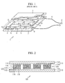
- FIG. 1 is a partially sectioned perspective view schematically showing a general thermoelectric element module.
- the conventional thermoelectric element module 1 includes P-type thermoelectric materials 3 and N-type thermoelectric materials 5. Electrodes 9 are attached in a predetermined pattern to a pair of insulation substrates 7 made of ceramic or silicon nitride. Such materials 3 and 5 are connected to the electrodes 9 in series.
- thermoelectric element module 1 if a DC current is applied to the electrode 9 through a lead wire 4 connected to a terminal 2, heat is generated at a side where the current flows from the P-type thermoelectric material 3 to the N-type thermoelectric material 5, and on the contrary heat is absorbed at a side where the current flows from the N-type thermoelectric material 5 to the P-type thermoelectric material 3, by means of the Peltier effect.
- the insulation substrate 7 joined to the heat-generating side is heated, and the insulation substrate 7 joined to the heat-absorbing side is cooled.
- the thermoelectric element module 1 if the polarity of the DC current applied to the terminal 2 is reversed, the heat-generating side is replaced with the heat-absorbing side.
- thermoelectric element module 1 if different temperatures are endowed to the pair of insulation substrates 7, voltage is generated at the terminal by means of the Seebeck effect.
- thermoelectric element is used as a module in which several ten or several hundred PN junction pairs are connected in series, as an example.
- Common thermoelectric element modules are manufactured by mechanically processing a thermoelectric material, which is a single crystal but has an ingot shape made by the directional solidification, into an element of a specific dimension, then joining electrodes to a patterned substrate made of ceramic or silicon nitride, and then joining the electrodes with thermoelectric materials (P-type, N-type). Each of the thermoelectric materials is joined to a corresponding electrode using an adhesive.
- Bi-Te thermoelectric material of a single crystal or directional solidifier has an inherent plane of cleavage in a crystallographic aspect, so the thermoelectric material may be easily cracked when being processed, which results in a deteriorated recovery rate.
- thermoelectric element when manufacturing a thermoelectric element, two joining processes are required. For example, after the electrodes are joined to a metal-plated ceramic substrate, thermoelectric materials should be joined to the electrodes. In this reason, it is complicated to manufacture a thermoelectric element, and also it is difficult to select a joining solder.
- a conventional thermoelectric element module manufacturing method several hundred (about 200) thermoelectric material dices of a substantially cuboid shape are manually soldered to an electrode of a substrate, which consumes a lot of labor. Thus, it is substantially impossible to lower a production cost below $10-$20 per each unit.
- precise dimension control is not ensured, a gap is formed between the thermoelectric material and the electrode, which may cause an inferior junction.
- thermoelectric element module it may also be considered to mass-product wafer-type thermoelectric elements by means of sputtering, used in a semiconductor manufacture process, in order to lower a price of the module.
- the element has a very small size, so it is difficult to increase the size of the thermoelectric element module.
- the present invention is designed to solve the problems of the prior art, and therefore it is an object of the present invention to provide a method for manufacturing a thermoelectric element of a thermoelectric pair shape, which allows larger size and automation; and a module of the thermoelectric element manufactured by the method.
- the present invention provides a method for manufacturing a thermoelectric element in which P-type thermoelectric materials and N-type thermoelectric materials are alternately joined between a pair of substrates, which includes: (a) preparing a P-type thermoelectric mixture powder and a N-type thermoelectric mixture powder in which a thermoelectric material powder and a low-melting metal powder are mixed at a predetermined ratio, respectively; (b) locating a support having a plurality of holes with a predetermined pattern on a first substrate; (c) injecting the P-type thermoelectric mixture powder and the N-type thermoelectric mixture powder into the corresponding holes of the support; (d) packing the P-type and N-type thermoelectric mixture powders injected into the holes; (e) separating the support from the first substrate; (f) locating a second substrate to the other side of the thermoelectric mixture powders to be opposite to the first substrate; and (g) thermally treating the thermoelectric mixture powders at a temperature lower than a melt point of the thermoelectric material to join
- thermoelectric element in which P-type thermoelectric materials and N-type thermoelectric materials are alternately joined between a pair of substrates, which includes: (a) preparing a P-type thermoelectric mixture powder and a N-type thermoelectric mixture powder by mixing a thermoelectric material powder and a low-melting metal powder at a predetermined ratio, respectively; (b) locating a support having a plurality of holes with a predetermined pattern on a first substrate; (c) injecting and packing the P-type thermoelectric mixture powder and the N-type thermoelectric mixture powder into the corresponding holes of the support; (d) thermally treating the thermoelectric mixture powders at a temperature lower than a melt point of the thermoelectric material to join the thermoelectric mixture powders to the first substrate by means of the melted low-melting metal; (e) separating the support from the first substrate in a state that the thermoelectric mixture powders are adhered to the first substrate; (f) locating a second substrate to the other
- the low-melting metal powder includes any one selected from the group consisting of Bi, Tl, Sn, P, Pb and Cd.
- the thermoelectric mixture powder includes a thermoelectric material powder and about 0.25 to 10 weight% of low-melting metal powder.
- the support includes a first support used for filling the P-type thermoelectric mixture powder and a second support used for filling the N-type thermoelectric mixture powder separately.
- the first and second substrates include an insulation member and a plurality of copper electrodes joined to the insulation member with a predetermined pattern, respectively.
- the insulation member includes aluminum oxide.
- the method further includes forming a nickel buffer layer on at least one surface of the first and second substrates.
- thermoelectric element module in which P-type thermoelectric materials and N-type thermoelectric materials are alternately joined between a pair of substrates, wherein the thermoelectric materials include a thermoelectric mixture powder in which a thermoelectric material powder and a low-melting metal powder are mixed at a predetermined ratio, and wherein the thermoelectric mixture powder is thermally treated at a temperature lower than a melt point of the thermoelectric material, the thermoelectric mixture powder is formed as the low-melting metal is melted, and at the same time both ends of the thermoelectric materials are joined to the pair of substrates.
- the low-melting metal powder includes any one selected from the group consisting of Bi, Tl, Sn, P, Pb and Cd.
- the thermoelectric mixture powder includes a thermoelectric material powder and about 0.25 to 10 weight% of low-melting metal powder.
- thermoelectric element module further includes a nickel buffer layer interposed between the substrate and the thermoelectric mixture powders.
- the substrate includes an insulation member and a plurality of copper electrodes formed on the insulation member with a predetermined pattern.
- the insulation member includes aluminum oxide.
- thermoelectric mixture powder in which N-type or P-type thermoelectric material powder is mixed with a low-melting metal powder having a lower melt point is injected into a support (or, a jig) having holes with a predetermined pattern, and then the low-melting metal is melted at a predetermined temperature to form P-type and N-type thermoelectric materials, respectively.
- a joining process for joining the thermoelectric material to a corresponding substrate may be automated.
- thermoelectric element manufacturing method and the thermoelectric element module according to the present invention ensure use thermoelectric powder, the size of the thermoelectric element module may be greatly increased.
- thermoelectric element module and a method for manufacturing the same according to preferred embodiments of the present invention will be described in detail with reference to the accompanying drawings.
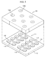
- FIG. 2 is a sectional view schematically showing a thermoelectric element module according to a preferred embodiment of the present invention.
- a thermoelectric element module 100 includes a pair of substrates 110, each having an insulation member 112 and a plurality of electrodes 114 joined to a surface of the insulation member 112 with a predetermined pattern, buffer layers 116 interposed between surfaces of the electrodes 114 opposite to the substrates 110 and having an area corresponding to P-type and N-type thermoelectric portions, and P-type and N-type thermoelectric mixture powders 120 contacted with the buffer layers 116 or the electrodes 114 and melted at a predetermined temperature to fix their shapes.
- Each substrate 110 includes the insulation member 112 made of aluminum oxide or the like and having a plate shape, and a plurality of electrodes 114 joined to one surface of the insulation member 112 and made of copper or the like.
- one electrode 114 preferably has so sufficient size and shape to ensure contact with ends of adjacent P-type and N-type thermoelectric mixture powders 120, respectively.
- the buffer layer 116 may be selectively used in this embodiment.
- the buffer layer 116 is formed on the electrodes 114 containing copper by means of plating (using nickel) or the like.
- the buffer layer 116 plays a role of preventing the thermoelectric mixture powder 120 from being dispersed to corresponding electrodes 114. Thus, in this embodiment, if the buffer layers 116 are excluded, the electrodes 114 are directly contacted with the corresponding thermoelectric mixture powders 120.
- the P-type and N-type thermoelectric mixture powders 120 include a thermoelectric material powder 122 and a low-melting metal powder 124, mixed at a predetermined ratio.
- thermoelectric material powder 122 may use thermoelectric semiconductor materials well known in the art, for example Bi-Te material, Fe-Si material, Si-Ge material and Co-Sb material, among which Bi-Te material is preferred.
- the low-melting metal powder 124 includes metal powders having a relatively lower melt point than a melt point of the thermoelectric material (for example, 450°C in case of Te).
- the low-melting metal powder 124 may be Bi (with a melt point of 271°C), Tl (with a melt point of 303.5°C), Sn (with a melt point of 232°C), P (with a melt point of 44°C), Pb (with a melt point of 327°C), Cd (with a melt point of 321°C) and so on.
- the thermoelectric mixture powder 120 is preferably prepared by mixing the above thermoelectric material powder 122 with 0.25 to 10 weight% of low-melting metal powder 124. Also, the thermoelectric mixture powder 120 is injected into holes 132 of a jig-type support 130 as explained below, and then thermally treated at a temperature higher than a melt point of the low-melting metal powder 124 and lower than a melt point of the thermoelectric material powder 122. After that, the thermoelectric mixture powder 120 is formed as the low-melting metal powder 124 is melted, and at the same time both ends of the thermoelectric mixture powder 120 are joined to the electrodes 114 or the buffer layers 116.
- FIG. 3 is an exploded perspective view schematically illustrating a method for manufacturing a thermoelectric element according to a preferred embodiment of the present invention.
- an upper substrate 113 has an insulation member 112 and electrodes 114 attached to a lower surface of the insulation member 112, and a lower substrate 111 has an insulation member 112 and electrodes 114 attached to an upper surface of the insulation member 112.
- thermoelectric material powder 122 and the low-melting metal powder 124 are mixed at a predetermined ratio (preferably, the thermoelectric material powder and about 0.25 to 10 weight% of low-melting metal powder) to prepare P-type and N-type thermoelectric mixture powders 120 (see FIG. 2 ).
- a pair of substrates 110 is prepared.
- Such substrates 110 are configured such that a plurality of electrodes 114 made of copper or the like are joined on the insulation member 112 made of aluminum oxide or the like and having a plate shape, as mentioned above.
- the lower substrate is referred to as a first substrate 111
- the upper substrate is referred to as a second substrate 113, for convenient explanation.
- P-type and N-type thermoelectric mixture powders are alternately arranged adjacently in four rows and four columns (4x4) and connected in series, and the thermoelectric mixture powder 120 is formed with a cylindrical shape.
- each of the electrodes 114 preferably has a cuboid shape as a whole, but its end is rounded into a hemispherical shape. It should be understood that the shape of such electrodes 114 may be changed as necessary in accordance with design conditions demanded by the module 100, particularly a sectional shape of the thermoelectric mixture powder 120 to be formed.
- the electrodes 114 arranged on the insulation member 112 may have any pattern if the P-type and N-type thermoelectric mixture powders 120 may be connected in series.
- the electrodes 114 are arranged in parallel, but in case of the second substrate 113 at an upper side, electrodes in a center portion are parallel with each other but electrodes at both edges are arranged perpendicular to the electrodes in the center portion.
- the support 130 having a plurality of holes 132 formed with a predetermined pattern is prepared.
- the support 130 is an integrated support in which holes 132a for the P-type thermoelectric mixture powder (hereinafter, referred to as P-type holes) and holes 132b for the N-type thermoelectric mixture powder (hereinafter, referred to as N-type holes) are alternately arranged such that the P-type and N-type thermoelectric mixture powders 120 are injected therein.
- the holes 132a and 132b of the integrated support 130 have predetermined diameter and height.
- the support 130 is located on the first substrate 111.
- a separate positioning mechanism (not shown) is preferably used so as to accurately match the positions of the electrodes 114 of the first electrode 111 with the holes 132 of the support 130.
- the support 130 is fixed with respect to the first substrate 111.
- the P-type and N-type thermoelectric mixture powders are respectively injected into the corresponding holes 132 of the integrated support 130.
- This injection process preferably employs an injector or blade (not shown).
- the thermoelectric mixture is preferably packed using a separate cylinder (not shown).
- This injection and/or packing process may also be performed without using the integrated support 130 as mentioned above.
- thermoelectric mixture powder 120 keeps, for example, a rod-type pellet shape by means of the above packing process.
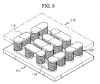
- the second substrate 113 is located at the other side of the thermoelectric mixture powder (for example, the rod) to be opposite to the first substrate 111.
- This work is preferably performed using a separate positioning means or mechanism, not shown.
- the pellet-type intermediate product having the thermoelectric mixture powder 120 located between the first substrate 111 and the second substrate 113 is thermally treated at a temperature lower than the melt point of the thermoelectric material and higher than the melt point of the low-melting metal.
- the low-melting metal powder 124 included in the pellet is melted to form a pellet itself, and at the same time the low-melting metal powders 124 at the ends of the pellet are fused (or, joined) to the first and second substrates 111 and 113, respectively.
- the support 130 is not removed from the first substrate 111.
- the thermoelectric mixture powder 120 is thermally treated at a temperature higher than the melt point of the low-melting metal and lower than the melt point of the thermoelectric material within a predetermined space in that state to primarily form the thermoelectric mixture powder 120 and also one end of the pellet is joined to the first substrate 111.
- the support 130 is separated from the first substrate 111, and then the second substrate 113 is located at the other side of the pellet.
- the pellet is secondarily heated (under the same conditions as the primary heating) to join the other end of the pellet to the second substrate.
- the joining process between the other end of the pellet and the second substrate 113 may be performed together with soldering, laser welding or the like, which may also be performed as a separate process.
Landscapes
- Engineering & Computer Science (AREA)
- Manufacturing & Machinery (AREA)
- Chemical & Material Sciences (AREA)
- Inorganic Chemistry (AREA)
- Powder Metallurgy (AREA)
Abstract
Description
- The present invention relates to a THERMOELECTRIC ELEMENT MODULE AND MANUFACTURING METHOD, and more particularly to a thermocouple-type thermoelectric module configured such that P-type thermoelectric materials and N-type thermoelectric materials are respectively joined between a pair of electrodes, and a method for manufacturing the thermoelectric element.
- Generally, a thermoelectric element including a thermoelectric converter is configured such that P-type thermoelectric materials and N-type thermoelectric materials are joined between metal electrodes to form a PN junction pair. If different temperatures are endowed to such a PN junction pair, a power is generated due to the Seebeck effect, so the thermoelectric element may function as a power generator. Also, due to the Peltier effect by which one side of the PN junction pair is cooled and the other side is heated, the thermoelectric element may be used as a temperature controller.
-
FIG. 1 is a partially sectioned perspective view schematically showing a general thermoelectric element module. Referring toFIG. 1 , the conventional thermoelectric element module 1 includes P-typethermoelectric materials 3 and N-typethermoelectric materials 5.Electrodes 9 are attached in a predetermined pattern to a pair ofinsulation substrates 7 made of ceramic or silicon nitride.Such materials electrodes 9 in series. - In the conventional thermoelectric element module 1, if a DC current is applied to the
electrode 9 through alead wire 4 connected to aterminal 2, heat is generated at a side where the current flows from the P-typethermoelectric material 3 to the N-typethermoelectric material 5, and on the contrary heat is absorbed at a side where the current flows from the N-typethermoelectric material 5 to the P-typethermoelectric material 3, by means of the Peltier effect. Thus, theinsulation substrate 7 joined to the heat-generating side is heated, and theinsulation substrate 7 joined to the heat-absorbing side is cooled. Meanwhile, in the thermoelectric element module 1, if the polarity of the DC current applied to theterminal 2 is reversed, the heat-generating side is replaced with the heat-absorbing side. Also, in the thermoelectric element module 1, if different temperatures are endowed to the pair ofinsulation substrates 7, voltage is generated at the terminal by means of the Seebeck effect. - In general, the thermoelectric element is used as a module in which several ten or several hundred PN junction pairs are connected in series, as an example. Common thermoelectric element modules are manufactured by mechanically processing a thermoelectric material, which is a single crystal but has an ingot shape made by the directional solidification, into an element of a specific dimension, then joining electrodes to a patterned substrate made of ceramic or silicon nitride, and then joining the electrodes with thermoelectric materials (P-type, N-type). Each of the thermoelectric materials is joined to a corresponding electrode using an adhesive.
- However, Bi-Te thermoelectric material of a single crystal or directional solidifier has an inherent plane of cleavage in a crystallographic aspect, so the thermoelectric material may be easily cracked when being processed, which results in a deteriorated recovery rate.
- In addition, when manufacturing a thermoelectric element, two joining processes are required. For example, after the electrodes are joined to a metal-plated ceramic substrate, thermoelectric materials should be joined to the electrodes. In this reason, it is complicated to manufacture a thermoelectric element, and also it is difficult to select a joining solder. In more detail, in a conventional thermoelectric element module manufacturing method, several hundred (about 200) thermoelectric material dices of a substantially cuboid shape are manually soldered to an electrode of a substrate, which consumes a lot of labor. Thus, it is substantially impossible to lower a production cost below $10-$20 per each unit. In addition, if precise dimension control is not ensured, a gap is formed between the thermoelectric material and the electrode, which may cause an inferior junction.
- Meanwhile, it may also be considered to mass-product wafer-type thermoelectric elements by means of sputtering, used in a semiconductor manufacture process, in order to lower a price of the module. However, in this case, the element has a very small size, so it is difficult to increase the size of the thermoelectric element module.
- The present invention is designed to solve the problems of the prior art, and therefore it is an object of the present invention to provide a method for manufacturing a thermoelectric element of a thermoelectric pair shape, which allows larger size and automation; and a module of the thermoelectric element manufactured by the method.
- In order to accomplish the above object, the present invention provides a method for manufacturing a thermoelectric element in which P-type thermoelectric materials and N-type thermoelectric materials are alternately joined between a pair of substrates, which includes: (a) preparing a P-type thermoelectric mixture powder and a N-type thermoelectric mixture powder in which a thermoelectric material powder and a low-melting metal powder are mixed at a predetermined ratio, respectively; (b) locating a support having a plurality of holes with a predetermined pattern on a first substrate; (c) injecting the P-type thermoelectric mixture powder and the N-type thermoelectric mixture powder into the corresponding holes of the support; (d) packing the P-type and N-type thermoelectric mixture powders injected into the holes; (e) separating the support from the first substrate; (f) locating a second substrate to the other side of the thermoelectric mixture powders to be opposite to the first substrate; and (g) thermally treating the thermoelectric mixture powders at a temperature lower than a melt point of the thermoelectric material to join the thermoelectric mixture powders to the first and second substrates.
- In another aspect of the present invention, there is also provided a method for manufacturing a thermoelectric element in which P-type thermoelectric materials and N-type thermoelectric materials are alternately joined between a pair of substrates, which includes: (a) preparing a P-type thermoelectric mixture powder and a N-type thermoelectric mixture powder by mixing a thermoelectric material powder and a low-melting metal powder at a predetermined ratio, respectively; (b) locating a support having a plurality of holes with a predetermined pattern on a first substrate; (c) injecting and packing the P-type thermoelectric mixture powder and the N-type thermoelectric mixture powder into the corresponding holes of the support; (d) thermally treating the thermoelectric mixture powders at a temperature lower than a melt point of the thermoelectric material to join the thermoelectric mixture powders to the first substrate by means of the melted low-melting metal; (e) separating the support from the first substrate in a state that the thermoelectric mixture powders are adhered to the first substrate; (f) locating a second substrate to the other side of the thermoelectric mixture powders to be opposite to the first substrate; and (g) thermally treating the thermoelectric mixture powders at a temperature lower than a melt point of the thermoelectric material to join the other side of the thermoelectric mixture powders to the second substrate.
- Preferably, the low-melting metal powder includes any one selected from the group consisting of Bi, Tl, Sn, P, Pb and Cd.
- Preferably, the thermoelectric mixture powder includes a thermoelectric material powder and about 0.25 to 10 weight% of low-melting metal powder.
- Preferably, in the step (b), the support includes a first support used for filling the P-type thermoelectric mixture powder and a second support used for filling the N-type thermoelectric mixture powder separately.
- Preferably, the first and second substrates include an insulation member and a plurality of copper electrodes joined to the insulation member with a predetermined pattern, respectively.
- Preferably, the insulation member includes aluminum oxide.
- Preferably, the method further includes forming a nickel buffer layer on at least one surface of the first and second substrates.
- In still another aspect of the present invention, there is also provided a thermoelectric element module in which P-type thermoelectric materials and N-type thermoelectric materials are alternately joined between a pair of substrates, wherein the thermoelectric materials include a thermoelectric mixture powder in which a thermoelectric material powder and a low-melting metal powder are mixed at a predetermined ratio, and wherein the thermoelectric mixture powder is thermally treated at a temperature lower than a melt point of the thermoelectric material, the thermoelectric mixture powder is formed as the low-melting metal is melted, and at the same time both ends of the thermoelectric materials are joined to the pair of substrates.
- Preferably, the low-melting metal powder includes any one selected from the group consisting of Bi, Tl, Sn, P, Pb and Cd.
- Preferably, the thermoelectric mixture powder includes a thermoelectric material powder and about 0.25 to 10 weight% of low-melting metal powder.
- Preferably, the thermoelectric element module further includes a nickel buffer layer interposed between the substrate and the thermoelectric mixture powders.
- Preferably, the substrate includes an insulation member and a plurality of copper electrodes formed on the insulation member with a predetermined pattern.
- Preferably, the insulation member includes aluminum oxide.
- In the method for manufacturing a thermoelectric element and the thermoelectric element module manufactured by the same according to the present invention, a thermoelectric mixture powder in which N-type or P-type thermoelectric material powder is mixed with a low-melting metal powder having a lower melt point is injected into a support (or, a jig) having holes with a predetermined pattern, and then the low-melting metal is melted at a predetermined temperature to form P-type and N-type thermoelectric materials, respectively. In addition, a joining process for joining the thermoelectric material to a corresponding substrate may be automated.
- In addition, since the thermoelectric element manufacturing method and the thermoelectric element module according to the present invention ensure use thermoelectric powder, the size of the thermoelectric element module may be greatly increased.
- Other objects and aspects of the present invention will become apparent from the following description of embodiments with reference to the accompanying drawing in which:
-
FIG. 1 is a perspective view schematically showing a general thermoelectric element module using a ceramic substrate as an insulation substrate; -
FIG. 2 is a sectional view schematically showing a thermoelectric element module according to a preferred embodiment of the present invention; -
FIG. 3 is an exploded perspective view schematically illustrating a method for manufacturing a thermoelectric element according to a preferred embodiment of the present invention; -
FIGs. 4 and5 are exploded perspective views schematically showing a support used in a method for manufacturing a thermoelectric element according to another embodiment of the present invention; and -
FIGs. 6 to 8 are perspective views for illustrating the method for manufacturing a thermoelectric element according to the preferred embodiment of the present invention, whereFIG. 6 shows that the support is coupled with a substrate,FIG. 7 shows that the support is separated after a thermoelectric mixture powder is fused to the substrate, andFIG. 8 shows that a second substrate is disposed on the thermoelectric mixture powder. - Hereinafter, a thermoelectric element module and a method for manufacturing the same according to preferred embodiments of the present invention will be described in detail with reference to the accompanying drawings.
- Prior to the description, it should be understood that the terms used in the specification and the appended claims should not be construed as limited to general and dictionary meanings, but interpreted based on the meanings and concepts corresponding to technical aspects of the present invention on the basis of the principle that the inventor is allowed to define terms appropriately for the best explanation. Therefore, the description proposed herein is just a preferable example for the purpose of illustrations only, not intended to limit the scope of the invention, so it should be understood that other equivalents and modifications could be made thereto without departing from the spirit and scope of the invention.
-
FIG. 2 is a sectional view schematically showing a thermoelectric element module according to a preferred embodiment of the present invention. - Referring to
FIG. 2 , athermoelectric element module 100 according to a preferred embodiment of the present invention includes a pair ofsubstrates 110, each having aninsulation member 112 and a plurality ofelectrodes 114 joined to a surface of theinsulation member 112 with a predetermined pattern,buffer layers 116 interposed between surfaces of theelectrodes 114 opposite to thesubstrates 110 and having an area corresponding to P-type and N-type thermoelectric portions, and P-type and N-typethermoelectric mixture powders 120 contacted with thebuffer layers 116 or theelectrodes 114 and melted at a predetermined temperature to fix their shapes. - Each
substrate 110 includes theinsulation member 112 made of aluminum oxide or the like and having a plate shape, and a plurality ofelectrodes 114 joined to one surface of theinsulation member 112 and made of copper or the like. Here, oneelectrode 114 preferably has so sufficient size and shape to ensure contact with ends of adjacent P-type and N-typethermoelectric mixture powders 120, respectively. - The
buffer layer 116 may be selectively used in this embodiment. Thebuffer layer 116 is formed on theelectrodes 114 containing copper by means of plating (using nickel) or the like. Thebuffer layer 116 plays a role of preventing thethermoelectric mixture powder 120 from being dispersed tocorresponding electrodes 114. Thus, in this embodiment, if thebuffer layers 116 are excluded, theelectrodes 114 are directly contacted with the correspondingthermoelectric mixture powders 120. - The P-type and N-type
thermoelectric mixture powders 120 include a thermoelectric material powder 122 and a low-meltingmetal powder 124, mixed at a predetermined ratio. - The thermoelectric material powder 122 may use thermoelectric semiconductor materials well known in the art, for example Bi-Te material, Fe-Si material, Si-Ge material and Co-Sb material, among which Bi-Te material is preferred.
- The low-melting
metal powder 124 includes metal powders having a relatively lower melt point than a melt point of the thermoelectric material (for example, 450°C in case of Te). The low-meltingmetal powder 124 may be Bi (with a melt point of 271°C), Tl (with a melt point of 303.5°C), Sn (with a melt point of 232°C), P (with a melt point of 44°C), Pb (with a melt point of 327°C), Cd (with a melt point of 321°C) and so on. - The
thermoelectric mixture powder 120 is preferably prepared by mixing the above thermoelectric material powder 122 with 0.25 to 10 weight% of low-meltingmetal powder 124. Also, thethermoelectric mixture powder 120 is injected into holes 132 of a jig-type support 130 as explained below, and then thermally treated at a temperature higher than a melt point of the low-meltingmetal powder 124 and lower than a melt point of the thermoelectric material powder 122. After that, thethermoelectric mixture powder 120 is formed as the low-meltingmetal powder 124 is melted, and at the same time both ends of thethermoelectric mixture powder 120 are joined to theelectrodes 114 or the buffer layers 116. -
FIG. 3 is an exploded perspective view schematically illustrating a method for manufacturing a thermoelectric element according to a preferred embodiment of the present invention. - Referring to
FIG. 3 , anupper substrate 113 has aninsulation member 112 andelectrodes 114 attached to a lower surface of theinsulation member 112, and alower substrate 111 has aninsulation member 112 andelectrodes 114 attached to an upper surface of theinsulation member 112. Now, a method for manufacturing a thermoelectric element according to a preferred embodiment of the present invention is explained with reference toFIG. 3 . - First, the thermoelectric material powder 122 and the low-melting
metal powder 124 are mixed at a predetermined ratio (preferably, the thermoelectric material powder and about 0.25 to 10 weight% of low-melting metal powder) to prepare P-type and N-type thermoelectric mixture powders 120 (seeFIG. 2 ). - Then, a pair of
substrates 110 is prepared.Such substrates 110 are configured such that a plurality ofelectrodes 114 made of copper or the like are joined on theinsulation member 112 made of aluminum oxide or the like and having a plate shape, as mentioned above. Here, the lower substrate is referred to as afirst substrate 111, and the upper substrate is referred to as asecond substrate 113, for convenient explanation. In this embodiment, P-type and N-type thermoelectric mixture powders are alternately arranged adjacently in four rows and four columns (4x4) and connected in series, and thethermoelectric mixture powder 120 is formed with a cylindrical shape. Thus, each of theelectrodes 114 preferably has a cuboid shape as a whole, but its end is rounded into a hemispherical shape. It should be understood that the shape ofsuch electrodes 114 may be changed as necessary in accordance with design conditions demanded by themodule 100, particularly a sectional shape of thethermoelectric mixture powder 120 to be formed. - Meanwhile, the
electrodes 114 arranged on theinsulation member 112 may have any pattern if the P-type and N-type thermoelectric mixture powders 120 may be connected in series. For example, as shown inFIG. 3 , in case of thefirst substrate 111 located at a lower side, theelectrodes 114 are arranged in parallel, but in case of thesecond substrate 113 at an upper side, electrodes in a center portion are parallel with each other but electrodes at both edges are arranged perpendicular to the electrodes in the center portion. - Subsequently, the
support 130 having a plurality of holes 132 formed with a predetermined pattern is prepared. In this embodiment, thesupport 130 is an integrated support in whichholes 132a for the P-type thermoelectric mixture powder (hereinafter, referred to as P-type holes) and holes 132b for the N-type thermoelectric mixture powder (hereinafter, referred to as N-type holes) are alternately arranged such that the P-type and N-type thermoelectric mixture powders 120 are injected therein. Theholes integrated support 130 have predetermined diameter and height. However, as shown inFIGs. 4 and5 , it is also possible to separately use a P-type support 131 (seeFIG. 4 ) in which only theholes 132a used for injecting the P-typethermoelectric mixture powder 120 are formed or a N-type support 133 (seeFIG. 5 ) in which only theholes 132b used for injecting the N-typethermoelectric mixture powder 120 are formed. - Then, as shown in
FIG. 6 , thesupport 130 is located on thefirst substrate 111. During this process, a separate positioning mechanism (not shown) is preferably used so as to accurately match the positions of theelectrodes 114 of thefirst electrode 111 with the holes 132 of thesupport 130. In the following injection and/or packing process, thesupport 130 is fixed with respect to thefirst substrate 111. - Subsequently, the P-type and N-type thermoelectric mixture powders are respectively injected into the corresponding holes 132 of the
integrated support 130. This injection process preferably employs an injector or blade (not shown). Meanwhile, after thethermoelectric mixture powder 120 is sufficiently injected into theholes integrated support 130, or during the injection process, the thermoelectric mixture is preferably packed using a separate cylinder (not shown). This injection and/or packing process may also be performed without using theintegrated support 130 as mentioned above. In other words, it is possible to perform the injection and/or packing process for the N-type thermoelectric mixture powder by using the N-type support 133 after completing the injection and/or packing process only for the P-type thermoelectric mixture powder by using the P-type support 131. It just depends on a user's selection, and the order of such processes is not essential. - After that, the
support 130 is separated from thefirst substrate 111. Then, as shown inFIG. 7 , thethermoelectric mixture powder 120 keeps, for example, a rod-type pellet shape by means of the above packing process. - Subsequently, as shown in
FIG. 8 , thesecond substrate 113 is located at the other side of the thermoelectric mixture powder (for example, the rod) to be opposite to thefirst substrate 111. This work is preferably performed using a separate positioning means or mechanism, not shown. - Then, as explained above, the pellet-type intermediate product having the
thermoelectric mixture powder 120 located between thefirst substrate 111 and thesecond substrate 113 is thermally treated at a temperature lower than the melt point of the thermoelectric material and higher than the melt point of the low-melting metal. Then, the low-meltingmetal powder 124 included in the pellet is melted to form a pellet itself, and at the same time the low-meltingmetal powders 124 at the ends of the pellet are fused (or, joined) to the first andsecond substrates - In an alternative embodiment, after the
thermoelectric mixture powder 120 is injected into the holes 132 of thesupport 130 located on thefirst substrate 111 and then packed, thesupport 130 is not removed from thefirst substrate 111. Instead, thethermoelectric mixture powder 120 is thermally treated at a temperature higher than the melt point of the low-melting metal and lower than the melt point of the thermoelectric material within a predetermined space in that state to primarily form thethermoelectric mixture powder 120 and also one end of the pellet is joined to thefirst substrate 111. After that, thesupport 130 is separated from thefirst substrate 111, and then thesecond substrate 113 is located at the other side of the pellet. In this state, the pellet is secondarily heated (under the same conditions as the primary heating) to join the other end of the pellet to the second substrate. Meanwhile, the joining process between the other end of the pellet and thesecond substrate 113 may be performed together with soldering, laser welding or the like, which may also be performed as a separate process. - The present invention has been described in detail. However, it should be understood that the detailed description and specific examples, while indicating preferred embodiments of the invention, are given by way of illustration only, since various changes and modifications within the spirit and scope of the invention will become apparent to those skilled in the art from this detailed description.
Claims (16)
- A method for manufacturing a thermoelectric element in which P-type thermoelectric materials and N-type thermoelectric materials are alternately joined between a pair of substrates, the method comprising:(a) preparing a P-type thermoelectric mixture powder and a N-type thermoelectric mixture powder in which a thermoelectric material powder and a low-melting metal powder are mixed at a predetermined ratio, respectively;(b) locating a support having a plurality of holes with a predetermined pattern on a first substrate;(c) injecting the P-type thermoelectric mixture powder and the N-type thermoelectric mixture powder into the corresponding holes of the support;(d) packing the P-type and N-type thermoelectric mixture powders injected into the holes;(e) separating the support from the first substrate;(f) locating a second substrate to the other side of the thermoelectric mixture powders to be opposite to the first substrate; and(g) thermally treating the thermoelectric mixture powders at a temperature lower than a melt point of the thermoelectric material to join the thermoelectric mixture powders to the first and second substrates.
- A method for manufacturing a thermoelectric element in which P-type thermoelectric materials and N-type thermoelectric materials are alternately joined between a pair of substrates, the method comprising:(a) preparing a P-type thermoelectric mixture powder and a N-type thermoelectric mixture powder by mixing a thermoelectric material powder and a low-melting metal powder at a predetermined ratio, respectively;(b) locating a support having a plurality of holes with a predetermined pattern on a first substrate;(c) injecting and packing the P-type thermoelectric mixture powder and the N-type thermoelectric mixture powder into the corresponding holes of the support;(d) thermally treating the thermoelectric mixture powders at a temperature lower than a melt point of the thermoelectric material to join the thermoelectric mixture powders to the first substrate by means of the melted low-melting metal;(e) separating the support from the first substrate in a state that the thermoelectric mixture powders are adhered to the first substrate;(f) locating a second substrate to the other side of the thermoelectric mixture powders to be opposite to the first substrate; and(g) joining the other side of the thermoelectric mixture powders to the second substrate.
- The method for manufacturing a thermoelectric element according to 1 or 2,
wherein the low-melting metal powder includes any one selected from the group consisting of Bi, Tl, Sn, P, Pb and Cd. - The method for manufacturing a thermoelectric element according to 1 or 2,
wherein the thermoelectric mixture powder includes a thermoelectric material powder and about 0.25 to 10 weight% of low-melting metal powder. - The method for manufacturing a thermoelectric element according to 1 or 2,
wherein, in the step (b), the support includes a first support used for filling the P-type thermoelectric mixture powder and a second support used for filling the N-type thermoelectric mixture powder separately. - The method for manufacturing a thermoelectric element according to 1 or 2,
wherein the first and second substrates include an insulation member and a plurality of electrodes joined to the insulation member with a predetermined pattern, respectively. - The method for manufacturing a thermoelectric element according to 6,
wherein the insulation member includes aluminum oxide, and the electrode includes copper. - The method for manufacturing a thermoelectric element according to 1 or 2, further comprising:forming a buffer layer on at least one surface of the first and second substrates.
- The method for manufacturing a thermoelectric element according to 8,
wherein the buffer layer includes nickel. - A thermoelectric element module in which P-type thermoelectric materials and N-type thermoelectric materials are alternately joined between a pair of substrates,
wherein the thermoelectric materials include a thermoelectric mixture powder in which a thermoelectric material powder and a low-melting metal powder are mixed at a predetermined ratio, and
wherein the thermoelectric mixture powder is thermally treated at a temperature lower than a melt point of the thermoelectric material, the thermoelectric mixture powder is formed as the low-melting metal is melted, and at the same time both ends of the thermoelectric materials are joined to the pair of substrates. - The thermoelectric element module according to claim 10,
wherein the low-melting metal powder includes any one selected from the group consisting of Bi, Tl, Sn, P, Pb and Cd. - The thermoelectric element module according to claim 10 or 11,
wherein the thermoelectric mixture powder includes a thermoelectric material powder and about 0.25 to 10 weight% of low-melting metal powder. - The thermoelectric element module according to claim 10, further comprising:a buffer layer interposed between the substrate and the thermoelectric mixture powders.
- The thermoelectric element module according to claim 13, wherein the buffer layer includes nickel.
- The thermoelectric element module according to claim 10,
wherein the substrate includes an insulation member and a plurality of electrodes formed on the insulation member with a predetermined pattern. - The thermoelectric element module according to claim 10,
wherein electrode includes copper, and the insulation member includes aluminum oxide.
Applications Claiming Priority (3)
| Application Number | Priority Date | Filing Date | Title |
|---|---|---|---|
| KR20090009319 | 2009-02-05 | ||
| PCT/KR2010/000690 WO2010090460A2 (en) | 2009-02-05 | 2010-02-04 | Thermoelectric element module and thermoelectric element production method |
| KR1020100010371A KR101062129B1 (en) | 2009-02-05 | 2010-02-04 | Thermoelectric Modules and Thermoelectric Device Manufacturing Methods |
Publications (3)
| Publication Number | Publication Date |
|---|---|
| EP2395570A2 true EP2395570A2 (en) | 2011-12-14 |
| EP2395570A4 EP2395570A4 (en) | 2014-01-22 |
| EP2395570B1 EP2395570B1 (en) | 2016-04-06 |
Family
ID=42755874
Family Applications (1)
| Application Number | Title | Priority Date | Filing Date |
|---|---|---|---|
| EP10738744.1A Active EP2395570B1 (en) | 2009-02-05 | 2010-02-04 | Thermoelectric element production method |
Country Status (7)
| Country | Link |
|---|---|
| US (1) | US8889453B2 (en) |
| EP (1) | EP2395570B1 (en) |
| JP (1) | JP5241928B2 (en) |
| KR (1) | KR101062129B1 (en) |
| CN (1) | CN102308402B (en) |
| TW (1) | TWI415314B (en) |
| WO (1) | WO2010090460A2 (en) |
Cited By (2)
| Publication number | Priority date | Publication date | Assignee | Title |
|---|---|---|---|---|
| CN103396122A (en) * | 2013-08-09 | 2013-11-20 | 中国科学院宁波材料技术与工程研究所 | A novel Cd-Te based thermoelectric material and its preparation method |
| WO2016173758A1 (en) * | 2015-04-29 | 2016-11-03 | Robert Bosch Gmbh | Thermoelectric generator and method for producing a thermoelectric generator |
Families Citing this family (23)
| Publication number | Priority date | Publication date | Assignee | Title |
|---|---|---|---|---|
| CN104392933B (en) | 2007-08-21 | 2017-11-07 | 加州大学评议会 | Nanostructured with high-performance thermoelectric property |
| KR20120028687A (en) * | 2010-09-15 | 2012-03-23 | 삼성전기주식회사 | Asymmetry thermoelectric module and manufacturing method thereof |
| US9240328B2 (en) | 2010-11-19 | 2016-01-19 | Alphabet Energy, Inc. | Arrays of long nanostructures in semiconductor materials and methods thereof |
| US8736011B2 (en) | 2010-12-03 | 2014-05-27 | Alphabet Energy, Inc. | Low thermal conductivity matrices with embedded nanostructures and methods thereof |
| US9051175B2 (en) | 2012-03-07 | 2015-06-09 | Alphabet Energy, Inc. | Bulk nano-ribbon and/or nano-porous structures for thermoelectric devices and methods for making the same |
| FR2991207B1 (en) * | 2012-06-04 | 2014-05-16 | Commissariat Energie Atomique | METHOD FOR MANUFACTURING THERMOELECTRIC MATERIAL |
| US9257627B2 (en) | 2012-07-23 | 2016-02-09 | Alphabet Energy, Inc. | Method and structure for thermoelectric unicouple assembly |
| US9082930B1 (en) * | 2012-10-25 | 2015-07-14 | Alphabet Energy, Inc. | Nanostructured thermolectric elements and methods of making the same |
| JP5831468B2 (en) * | 2013-01-24 | 2015-12-09 | 株式会社デンソー | Method for manufacturing thermoelectric conversion device |
| US9309596B2 (en) * | 2013-01-31 | 2016-04-12 | Ngimat Co. | Flame-assisted flash sintering |
| US10388846B2 (en) * | 2014-03-28 | 2019-08-20 | Matrix Industries, Inc. | Formation of a densified object from powdered precursor materials |
| US9691849B2 (en) | 2014-04-10 | 2017-06-27 | Alphabet Energy, Inc. | Ultra-long silicon nanostructures, and methods of forming and transferring the same |
| KR20160063000A (en) | 2014-11-26 | 2016-06-03 | 현대자동차주식회사 | Thermoelectric generation device |
| KR101724847B1 (en) | 2015-06-01 | 2017-04-18 | 현대자동차주식회사 | Thermoelectric Generation Device for vehicle |
| JP6721317B2 (en) | 2015-11-18 | 2020-07-15 | 日東電工株式会社 | Method of manufacturing semiconductor device |
| TWI570972B (en) * | 2016-01-20 | 2017-02-11 | 財團法人工業技術研究院 | Thermoelectric conversion device and thermoelectric converter |
| TWI608638B (en) | 2016-12-15 | 2017-12-11 | 財團法人工業技術研究院 | Thermoelectric module |
| CN108511590B (en) * | 2017-02-28 | 2019-08-16 | 杭州熵能热导科技有限公司 | A kind of thermoelectric module and its manufacturing method |
| CN109192851B (en) * | 2018-08-29 | 2020-12-29 | 武汉理工大学 | A method for preparing flexible thermoelectric thick film materials with excellent electrical transport properties by adding sintering aids |
| CN113272979B (en) | 2018-11-16 | 2024-12-27 | Ats知识产权有限责任公司 | Thermal lens electrodes for improved performance in thermoelectric generators |
| KR102693403B1 (en) * | 2019-11-22 | 2024-08-09 | 엘지이노텍 주식회사 | Thermo electric element |
| CN113629179A (en) * | 2021-08-10 | 2021-11-09 | 东莞先导先进科技有限公司 | Semiconductor thermoelectric device and preparation method thereof |
| KR102767000B1 (en) * | 2023-10-11 | 2025-02-14 | 알머티리얼즈 주식회사 | Low-cost, high-strength thermoelectric module manufacturing method that simplifies the manufacturing process |
Family Cites Families (21)
| Publication number | Priority date | Publication date | Assignee | Title |
|---|---|---|---|---|
| JP3472593B2 (en) | 1993-04-22 | 2003-12-02 | 小松エレクトロニクス株式会社 | Thermoelectric device |
| US6025554A (en) * | 1995-10-16 | 2000-02-15 | Macris; Chris | Thermoelectric device and method of manufacture |
| JPH09199766A (en) * | 1995-11-13 | 1997-07-31 | Ngk Insulators Ltd | Method for manufacturing thermoelectric conversion module |
| AU4551399A (en) | 1998-06-08 | 1999-12-30 | Ormet Corporation | Process for production of high performance thermoelectric modules and low temperature sinterable thermoelectric compositions therefor |
| US6207886B1 (en) * | 1998-06-30 | 2001-03-27 | Matsushita Electric Industrial Co., Ltd. | Skutterudite thermoelectric material thermoelectric couple and method of producing the same |
| JP2001028462A (en) * | 1999-07-13 | 2001-01-30 | Yamaha Corp | Thermoelectric element and method of manufacturing thermoelectric element |
| JP3600486B2 (en) * | 1999-08-24 | 2004-12-15 | セイコーインスツル株式会社 | Manufacturing method of thermoelectric conversion element |
| US6297441B1 (en) * | 2000-03-24 | 2001-10-02 | Chris Macris | Thermoelectric device and method of manufacture |
| JP4504523B2 (en) * | 2000-07-13 | 2010-07-14 | 旭化成株式会社 | Thermoelectric material and manufacturing method thereof |
| US6410971B1 (en) * | 2001-07-12 | 2002-06-25 | Ferrotec (Usa) Corporation | Thermoelectric module with thin film substrates |
| JP2003046146A (en) | 2001-07-30 | 2003-02-14 | Komatsu Ltd | Thermoelectric modular temperature controller |
| JP2003174202A (en) * | 2001-09-25 | 2003-06-20 | Sumitomo Electric Ind Ltd | Thermoelectric device, optical module using the same, and methods of manufacturing these |
| CA2377340A1 (en) * | 2001-09-25 | 2003-03-25 | Sumitomo Electric Industries, Ltd. | Thermoelectric device and optical module made with the device and method for producing them |
| JP2005340559A (en) | 2004-05-28 | 2005-12-08 | Kyocera Corp | Ceramic substrate for thermoelectric exchange module |
| US20060157101A1 (en) | 2004-10-29 | 2006-07-20 | Sakamoto Jeff S | System and method for fabrication of high-efficiency durable thermoelectric devices |
| KR100926851B1 (en) * | 2004-12-20 | 2009-11-13 | 가부시끼가이샤 도시바 | Thermoelectric conversion module, heat exchanger using same, and thermoelectric power generating system |
| JP3879769B1 (en) * | 2006-02-22 | 2007-02-14 | 株式会社村田製作所 | Thermoelectric conversion module and manufacturing method thereof |
| DE102006055120B4 (en) * | 2006-11-21 | 2015-10-01 | Evonik Degussa Gmbh | Thermoelectric elements, process for their preparation and their use |
| JP4912931B2 (en) * | 2007-03-22 | 2012-04-11 | 住友化学株式会社 | Thermoelectric conversion module manufacturing method and thermoelectric conversion module |
| US8193439B2 (en) * | 2009-06-23 | 2012-06-05 | Laird Technologies, Inc. | Thermoelectric modules and related methods |
| KR20120028687A (en) * | 2010-09-15 | 2012-03-23 | 삼성전기주식회사 | Asymmetry thermoelectric module and manufacturing method thereof |
-
2010
- 2010-02-04 WO PCT/KR2010/000690 patent/WO2010090460A2/en not_active Ceased
- 2010-02-04 JP JP2011549064A patent/JP5241928B2/en active Active
- 2010-02-04 US US13/148,007 patent/US8889453B2/en active Active
- 2010-02-04 CN CN201080006622.5A patent/CN102308402B/en active Active
- 2010-02-04 TW TW099103350A patent/TWI415314B/en active
- 2010-02-04 KR KR1020100010371A patent/KR101062129B1/en active Active
- 2010-02-04 EP EP10738744.1A patent/EP2395570B1/en active Active
Cited By (2)
| Publication number | Priority date | Publication date | Assignee | Title |
|---|---|---|---|---|
| CN103396122A (en) * | 2013-08-09 | 2013-11-20 | 中国科学院宁波材料技术与工程研究所 | A novel Cd-Te based thermoelectric material and its preparation method |
| WO2016173758A1 (en) * | 2015-04-29 | 2016-11-03 | Robert Bosch Gmbh | Thermoelectric generator and method for producing a thermoelectric generator |
Also Published As
| Publication number | Publication date |
|---|---|
| JP5241928B2 (en) | 2013-07-17 |
| WO2010090460A3 (en) | 2010-11-25 |
| US20110304004A1 (en) | 2011-12-15 |
| WO2010090460A2 (en) | 2010-08-12 |
| CN102308402B (en) | 2014-03-19 |
| KR20100090209A (en) | 2010-08-13 |
| EP2395570B1 (en) | 2016-04-06 |
| TW201044654A (en) | 2010-12-16 |
| JP2012517116A (en) | 2012-07-26 |
| US8889453B2 (en) | 2014-11-18 |
| EP2395570A4 (en) | 2014-01-22 |
| CN102308402A (en) | 2012-01-04 |
| TWI415314B (en) | 2013-11-11 |
| KR101062129B1 (en) | 2011-09-02 |
Similar Documents
| Publication | Publication Date | Title |
|---|---|---|
| EP2395570B1 (en) | Thermoelectric element production method | |
| EP2641281B1 (en) | Thermoelectric conversion element module | |
| CN101931044A (en) | Electrothermal module and correlation technique | |
| US20130118541A1 (en) | Thermoelectric module and method of manufacturing the same | |
| KR20150031216A (en) | Thermoelectric conversion module | |
| EP2975660A1 (en) | Thermoelectric conversion module | |
| JPH09199766A (en) | Method for manufacturing thermoelectric conversion module | |
| JP4284589B2 (en) | Thermoelectric semiconductor manufacturing method, thermoelectric conversion element manufacturing method, and thermoelectric conversion device manufacturing method | |
| US10236430B2 (en) | Thermoelectric module | |
| US10833237B2 (en) | Thermoelectric module | |
| JP2013542579A (en) | Method for manufacturing thermoelectric conversion element module | |
| JPH10313134A (en) | Manufacturing method of thermoelectric module | |
| JP3549426B2 (en) | Thermoelectric element and method for manufacturing the same | |
| RU2234765C1 (en) | Thermoelectric module | |
| JP2002353522A (en) | Thermoelectric element | |
| JP2990352B2 (en) | Thermoelectric element manufacturing method | |
| KR102333422B1 (en) | Bulk thermoelectric element and manufacturing method thereof | |
| JP3377944B2 (en) | Thermoelectric element and method of manufacturing the same | |
| JP2893258B1 (en) | Thermoelectric element and method of manufacturing the same | |
| JPH11233838A (en) | Thermoelectric element and method of manufacturing the same | |
| JP6139439B2 (en) | Thermoelectric module | |
| EP4275236A1 (en) | Thermoelectric module | |
| JPH1174570A (en) | Thermoelectric element and method of manufacturing the same | |
| JP2002190623A (en) | Thermoelectric element array unit, method of manufacturing the same, and thermoelectric module using thermoelectric element array unit | |
| JP2013004711A (en) | Thermoelectric conversion module and method of manufacturing the same |
Legal Events
| Date | Code | Title | Description |
|---|---|---|---|
| PUAI | Public reference made under article 153(3) epc to a published international application that has entered the european phase |
Free format text: ORIGINAL CODE: 0009012 |
|
| 17P | Request for examination filed |
Effective date: 20110727 |
|
| AK | Designated contracting states |
Kind code of ref document: A2 Designated state(s): AT BE BG CH CY CZ DE DK EE ES FI FR GB GR HR HU IE IS IT LI LT LU LV MC MK MT NL NO PL PT RO SE SI SK SM TR |
|
| DAX | Request for extension of the european patent (deleted) | ||
| A4 | Supplementary search report drawn up and despatched |
Effective date: 20131220 |
|
| RIC1 | Information provided on ipc code assigned before grant |
Ipc: H01L 35/32 20060101ALI20131216BHEP Ipc: H01L 35/16 20060101ALI20131216BHEP Ipc: H01L 35/34 20060101AFI20131216BHEP |
|
| GRAP | Despatch of communication of intention to grant a patent |
Free format text: ORIGINAL CODE: EPIDOSNIGR1 |
|
| INTG | Intention to grant announced |
Effective date: 20151117 |
|
| GRAS | Grant fee paid |
Free format text: ORIGINAL CODE: EPIDOSNIGR3 |
|
| GRAA | (expected) grant |
Free format text: ORIGINAL CODE: 0009210 |
|
| AK | Designated contracting states |
Kind code of ref document: B1 Designated state(s): AT BE BG CH CY CZ DE DK EE ES FI FR GB GR HR HU IE IS IT LI LT LU LV MC MK MT NL NO PL PT RO SE SI SK SM TR |
|
| REG | Reference to a national code |
Ref country code: GB Ref legal event code: FG4D |
|
| REG | Reference to a national code |
Ref country code: AT Ref legal event code: REF Ref document number: 788621 Country of ref document: AT Kind code of ref document: T Effective date: 20160415 Ref country code: CH Ref legal event code: EP |
|
| REG | Reference to a national code |
Ref country code: IE Ref legal event code: FG4D |
|
| REG | Reference to a national code |
Ref country code: DE Ref legal event code: R096 Ref document number: 602010032047 Country of ref document: DE |
|
| REG | Reference to a national code |
Ref country code: LT Ref legal event code: MG4D Ref country code: NL Ref legal event code: MP Effective date: 20160406 |
|
| REG | Reference to a national code |
Ref country code: AT Ref legal event code: MK05 Ref document number: 788621 Country of ref document: AT Kind code of ref document: T Effective date: 20160406 |
|
| PG25 | Lapsed in a contracting state [announced via postgrant information from national office to epo] |
Ref country code: NL Free format text: LAPSE BECAUSE OF FAILURE TO SUBMIT A TRANSLATION OF THE DESCRIPTION OR TO PAY THE FEE WITHIN THE PRESCRIBED TIME-LIMIT Effective date: 20160406 |
|
| PG25 | Lapsed in a contracting state [announced via postgrant information from national office to epo] |
Ref country code: PL Free format text: LAPSE BECAUSE OF FAILURE TO SUBMIT A TRANSLATION OF THE DESCRIPTION OR TO PAY THE FEE WITHIN THE PRESCRIBED TIME-LIMIT Effective date: 20160406 Ref country code: FI Free format text: LAPSE BECAUSE OF FAILURE TO SUBMIT A TRANSLATION OF THE DESCRIPTION OR TO PAY THE FEE WITHIN THE PRESCRIBED TIME-LIMIT Effective date: 20160406 Ref country code: IS Free format text: LAPSE BECAUSE OF FAILURE TO SUBMIT A TRANSLATION OF THE DESCRIPTION OR TO PAY THE FEE WITHIN THE PRESCRIBED TIME-LIMIT Effective date: 20160806 Ref country code: NO Free format text: LAPSE BECAUSE OF FAILURE TO SUBMIT A TRANSLATION OF THE DESCRIPTION OR TO PAY THE FEE WITHIN THE PRESCRIBED TIME-LIMIT Effective date: 20160706 Ref country code: LT Free format text: LAPSE BECAUSE OF FAILURE TO SUBMIT A TRANSLATION OF THE DESCRIPTION OR TO PAY THE FEE WITHIN THE PRESCRIBED TIME-LIMIT Effective date: 20160406 |
|
| PG25 | Lapsed in a contracting state [announced via postgrant information from national office to epo] |
Ref country code: GR Free format text: LAPSE BECAUSE OF FAILURE TO SUBMIT A TRANSLATION OF THE DESCRIPTION OR TO PAY THE FEE WITHIN THE PRESCRIBED TIME-LIMIT Effective date: 20160707 Ref country code: ES Free format text: LAPSE BECAUSE OF FAILURE TO SUBMIT A TRANSLATION OF THE DESCRIPTION OR TO PAY THE FEE WITHIN THE PRESCRIBED TIME-LIMIT Effective date: 20160406 Ref country code: PT Free format text: LAPSE BECAUSE OF FAILURE TO SUBMIT A TRANSLATION OF THE DESCRIPTION OR TO PAY THE FEE WITHIN THE PRESCRIBED TIME-LIMIT Effective date: 20160808 Ref country code: AT Free format text: LAPSE BECAUSE OF FAILURE TO SUBMIT A TRANSLATION OF THE DESCRIPTION OR TO PAY THE FEE WITHIN THE PRESCRIBED TIME-LIMIT Effective date: 20160406 Ref country code: SE Free format text: LAPSE BECAUSE OF FAILURE TO SUBMIT A TRANSLATION OF THE DESCRIPTION OR TO PAY THE FEE WITHIN THE PRESCRIBED TIME-LIMIT Effective date: 20160406 Ref country code: LV Free format text: LAPSE BECAUSE OF FAILURE TO SUBMIT A TRANSLATION OF THE DESCRIPTION OR TO PAY THE FEE WITHIN THE PRESCRIBED TIME-LIMIT Effective date: 20160406 Ref country code: HR Free format text: LAPSE BECAUSE OF FAILURE TO SUBMIT A TRANSLATION OF THE DESCRIPTION OR TO PAY THE FEE WITHIN THE PRESCRIBED TIME-LIMIT Effective date: 20160406 |
|
| PG25 | Lapsed in a contracting state [announced via postgrant information from national office to epo] |
Ref country code: BE Free format text: LAPSE BECAUSE OF FAILURE TO SUBMIT A TRANSLATION OF THE DESCRIPTION OR TO PAY THE FEE WITHIN THE PRESCRIBED TIME-LIMIT Effective date: 20160406 Ref country code: IT Free format text: LAPSE BECAUSE OF FAILURE TO SUBMIT A TRANSLATION OF THE DESCRIPTION OR TO PAY THE FEE WITHIN THE PRESCRIBED TIME-LIMIT Effective date: 20160406 |
|
| REG | Reference to a national code |
Ref country code: DE Ref legal event code: R097 Ref document number: 602010032047 Country of ref document: DE |
|
| REG | Reference to a national code |
Ref country code: FR Ref legal event code: PLFP Year of fee payment: 8 |
|
| PG25 | Lapsed in a contracting state [announced via postgrant information from national office to epo] |
Ref country code: RO Free format text: LAPSE BECAUSE OF FAILURE TO SUBMIT A TRANSLATION OF THE DESCRIPTION OR TO PAY THE FEE WITHIN THE PRESCRIBED TIME-LIMIT Effective date: 20160406 Ref country code: EE Free format text: LAPSE BECAUSE OF FAILURE TO SUBMIT A TRANSLATION OF THE DESCRIPTION OR TO PAY THE FEE WITHIN THE PRESCRIBED TIME-LIMIT Effective date: 20160406 Ref country code: DK Free format text: LAPSE BECAUSE OF FAILURE TO SUBMIT A TRANSLATION OF THE DESCRIPTION OR TO PAY THE FEE WITHIN THE PRESCRIBED TIME-LIMIT Effective date: 20160406 Ref country code: SK Free format text: LAPSE BECAUSE OF FAILURE TO SUBMIT A TRANSLATION OF THE DESCRIPTION OR TO PAY THE FEE WITHIN THE PRESCRIBED TIME-LIMIT Effective date: 20160406 Ref country code: CZ Free format text: LAPSE BECAUSE OF FAILURE TO SUBMIT A TRANSLATION OF THE DESCRIPTION OR TO PAY THE FEE WITHIN THE PRESCRIBED TIME-LIMIT Effective date: 20160406 |
|
| PLBE | No opposition filed within time limit |
Free format text: ORIGINAL CODE: 0009261 |
|
| STAA | Information on the status of an ep patent application or granted ep patent |
Free format text: STATUS: NO OPPOSITION FILED WITHIN TIME LIMIT |
|
| PG25 | Lapsed in a contracting state [announced via postgrant information from national office to epo] |
Ref country code: SM Free format text: LAPSE BECAUSE OF FAILURE TO SUBMIT A TRANSLATION OF THE DESCRIPTION OR TO PAY THE FEE WITHIN THE PRESCRIBED TIME-LIMIT Effective date: 20160406 |
|
| 26N | No opposition filed |
Effective date: 20170110 |
|
| PG25 | Lapsed in a contracting state [announced via postgrant information from national office to epo] |
Ref country code: SI Free format text: LAPSE BECAUSE OF FAILURE TO SUBMIT A TRANSLATION OF THE DESCRIPTION OR TO PAY THE FEE WITHIN THE PRESCRIBED TIME-LIMIT Effective date: 20160406 |
|
| PG25 | Lapsed in a contracting state [announced via postgrant information from national office to epo] |
Ref country code: MC Free format text: LAPSE BECAUSE OF FAILURE TO SUBMIT A TRANSLATION OF THE DESCRIPTION OR TO PAY THE FEE WITHIN THE PRESCRIBED TIME-LIMIT Effective date: 20160406 |
|
| REG | Reference to a national code |
Ref country code: CH Ref legal event code: PL |
|
| GBPC | Gb: european patent ceased through non-payment of renewal fee |
Effective date: 20170204 |
|
| PG25 | Lapsed in a contracting state [announced via postgrant information from national office to epo] |
Ref country code: LI Free format text: LAPSE BECAUSE OF NON-PAYMENT OF DUE FEES Effective date: 20170228 Ref country code: CH Free format text: LAPSE BECAUSE OF NON-PAYMENT OF DUE FEES Effective date: 20170228 |
|
| REG | Reference to a national code |
Ref country code: IE Ref legal event code: MM4A |
|
| PG25 | Lapsed in a contracting state [announced via postgrant information from national office to epo] |
Ref country code: LU Free format text: LAPSE BECAUSE OF NON-PAYMENT OF DUE FEES Effective date: 20170204 |
|
| REG | Reference to a national code |
Ref country code: FR Ref legal event code: PLFP Year of fee payment: 9 |
|
| PG25 | Lapsed in a contracting state [announced via postgrant information from national office to epo] |
Ref country code: GB Free format text: LAPSE BECAUSE OF NON-PAYMENT OF DUE FEES Effective date: 20170204 Ref country code: IE Free format text: LAPSE BECAUSE OF NON-PAYMENT OF DUE FEES Effective date: 20170204 |
|
| PG25 | Lapsed in a contracting state [announced via postgrant information from national office to epo] |
Ref country code: MT Free format text: LAPSE BECAUSE OF NON-PAYMENT OF DUE FEES Effective date: 20170204 |
|
| PG25 | Lapsed in a contracting state [announced via postgrant information from national office to epo] |
Ref country code: HU Free format text: LAPSE BECAUSE OF FAILURE TO SUBMIT A TRANSLATION OF THE DESCRIPTION OR TO PAY THE FEE WITHIN THE PRESCRIBED TIME-LIMIT; INVALID AB INITIO Effective date: 20100204 |
|
| PG25 | Lapsed in a contracting state [announced via postgrant information from national office to epo] |
Ref country code: BG Free format text: LAPSE BECAUSE OF FAILURE TO SUBMIT A TRANSLATION OF THE DESCRIPTION OR TO PAY THE FEE WITHIN THE PRESCRIBED TIME-LIMIT Effective date: 20160406 |
|
| PG25 | Lapsed in a contracting state [announced via postgrant information from national office to epo] |
Ref country code: CY Free format text: LAPSE BECAUSE OF NON-PAYMENT OF DUE FEES Effective date: 20160406 |
|
| PG25 | Lapsed in a contracting state [announced via postgrant information from national office to epo] |
Ref country code: MK Free format text: LAPSE BECAUSE OF FAILURE TO SUBMIT A TRANSLATION OF THE DESCRIPTION OR TO PAY THE FEE WITHIN THE PRESCRIBED TIME-LIMIT Effective date: 20160406 |
|
| PG25 | Lapsed in a contracting state [announced via postgrant information from national office to epo] |
Ref country code: TR Free format text: LAPSE BECAUSE OF FAILURE TO SUBMIT A TRANSLATION OF THE DESCRIPTION OR TO PAY THE FEE WITHIN THE PRESCRIBED TIME-LIMIT Effective date: 20160406 |
|
| REG | Reference to a national code |
Ref country code: DE Ref legal event code: R079 Ref document number: 602010032047 Country of ref document: DE Free format text: PREVIOUS MAIN CLASS: H01L0035340000 Ipc: H10N0010010000 |
|
| PGFP | Annual fee paid to national office [announced via postgrant information from national office to epo] |
Ref country code: DE Payment date: 20260120 Year of fee payment: 17 |
|
| PGFP | Annual fee paid to national office [announced via postgrant information from national office to epo] |
Ref country code: FR Payment date: 20260121 Year of fee payment: 17 |